Surface termination passivation of imidazole-based diiodide enabling efficient inverted perovskite solar cells†
Yu
Wang
ab,
Jiaxing
Song
 *a,
Jingchuan
Ye
ab,
Yingzhi
Jin
a,
Xinxing
Yin
 a,
Zhen
Su
a,
Lin
Hu
a,
Zhen
Su
a,
Lin
Hu
 a,
Yan
Wu
a,
Chufeng
Qiu
a,
Hao
Wang
a,
Wensheng
Yan
*b and
Zaifang
Li
a,
Yan
Wu
a,
Chufeng
Qiu
a,
Hao
Wang
a,
Wensheng
Yan
*b and
Zaifang
Li
 *a
*a
aChina-Australia Institute for Advanced Materials and Manufacturing, Jiaxing University, Jiaxing 314001, P. R. China. E-mail: songjx@zjxu.edu.cn; zaifang.li@zjxu.edu.cn
bInstitute of Carbon Neutrality and New Energy, School of Electronics and Information, Hangzhou Dianzi University, Hangzhou, 310018, China. E-mail: wensheng.yan@hdu.edu.cn
First published on 1st May 2023
Abstract
N-(3-aminopropyl)-imidazole diiodide (APDI) was introduced on the upper surface of the perovskite for the first time to modulate the terminal groups. The defect traps were suppressed by binding N cations from the APDI with Pb2+. Consequently, the optimum APDI-treated device achieved a PCE of 21.41% and exhibited excellent stability.
Metal-halide perovskite materials are widely employed as photosensitive layers for the study of perovskite solar cells (PSCs) based on exotic semiconductor properties (e.g., tunable bandgap, excellent optical absorption, and high defect tolerance).1,2 Presently, the power conversion efficiency (PCE) of single-junction PSCs has increased from less than 4% in 2009 to 25.7%.1–3 Although the PCE of nip-type (regular) PSCs is always higher than that of pin-type (inverted) PSCs during the same period, the inverted PSCs are gradually receiving more attention owing to their lower preparation energy consumption.3 In addition, MA-free Cs/FA-based perovskite combines excellent stability, which is a desirable material choice for application in PSCs.4
The surface of the perovskite film, which is prepared by a solution-based process, suffers from various unavoidable defects (e.g., vacancies, interstitials, anti-site substitutions), resulting from the ionic nature of perovskite materials and the soft crystalline properties.5 Moreover, the properties of nanoscale-based perovskite films are susceptible to surface effect, making surface modulation engineering an effective means to regulate the chemical environment of the upper surface of perovskite films.6,7 Consequently, the presence of the above defects was considered a major factor restricting the further elevation in PSC performance, which not only induced a decrease in PCE by trapping charges to aggravate the nonradiative recombination but also served as the preferential sites for erosion by external factors (e.g., H2O, O2, and ultraviolet) to accelerate the degradation of perovskite film.4 To date, studies based on ligand engineering for perovskite surfaces have been broadly reported. For example, Lewis-base molecules with electron-donating groups are frequently employed to reduce uncoordinated Pb2+ that is considered to be the main source of defects on the perovskite surface due to its lower formation energy.5,7,8
Compared to the ligand engineering realized by molecules with electron-donating groups, the ammonium salt-based modification has the advantage of a convenient and efficient process for the passivation step.9,10 Since the work of interfacial modification by phenethylamine iodide (PEAI) was reported, the investigation of modulating the terminal environment of perovskites by ammonium salts had drawn attention. Amino-corannulene iodides were introduced on the surface of the perovskite by Yang et al., leading to a significant reduction of the Pb2+ traps owing to the favorable coordination ability between R-NH3+ and Pb2+.11 Simultaneously, ammonium diiodide salts, such as ethane-1,2-diamine diiodide, histamine diiodide, have also been adopted as modifiers to mitigate the defect density of perovskite at the top and bottom interface of PSCs.12,13 However, the above ammonium salts have only one functional group binding to the Pb2+ traps for passivation. Compared to the wide investigation of passivators with single-acting sites, there are few reports on ammonium salts with dual-functional groups of coordination for the surface modulation of perovskite.
In this study, we introduced the API (N-(3-Aminopropyl)-imidazole) diiodide (APDI) on the upper surface of FA0.83Cs0.17Pb(I0.86Br0.14)3 film to modulate the terminal chemical environment, and good photovoltaic performance was obtained. Table S1 (ESI†) lists a comparison of the parameters. The bifunctional groups (C![[double bond, length as m-dash]](https://www.rsc.org/images/entities/char_e001.gif) NH+– and -NH3+–) in APDI make it more effective in reducing the Pb2+ defect on the perovskite surface through bonding to Pb2+. Density functional theory (DFT) demonstrated that the N on the imidazole ring in APDI was slightly more inclined to bind to Pb2+ traps than to N on the branched chain. Moreover, the hydrophobicity of the perovskite films was enhanced by the introduction of APDI with an alkyl chain on the surface. Consequently, the optimum device after APDI modification (target) has an increased PCE, from 20.01% to 21.41%. Additionally, the target devices exhibited excellent stability, maintaining 78% and 90% of the initial PCE after 800 h and 1000 h of aging in air and nitrogen atmospheres, respectively.
NH+– and -NH3+–) in APDI make it more effective in reducing the Pb2+ defect on the perovskite surface through bonding to Pb2+. Density functional theory (DFT) demonstrated that the N on the imidazole ring in APDI was slightly more inclined to bind to Pb2+ traps than to N on the branched chain. Moreover, the hydrophobicity of the perovskite films was enhanced by the introduction of APDI with an alkyl chain on the surface. Consequently, the optimum device after APDI modification (target) has an increased PCE, from 20.01% to 21.41%. Additionally, the target devices exhibited excellent stability, maintaining 78% and 90% of the initial PCE after 800 h and 1000 h of aging in air and nitrogen atmospheres, respectively.
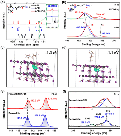
A reasonable APDI molecule based on interfacial engineering was designed to achieve synergistic enhancement of PSC performance. Unlike the isopropanol solution of APDI, pure API (which exists as a liquid at room temperature) contacting the perovskite causes rapid decomposition of thin films (Fig. S1a, ESI†). The molecular structures of API and APDI are shown in Fig. S1b (ESI†), and the details of APDI synthesis are shown in the Experimental Section. The H-NMR results showed that the chemical shifts of H in the iodinated API changed compared to the API. As depicted in Fig. 1a, the differences in chemical shift (ΔδH) between the iodinated API and API at the same position were as follows: ΔδHa = 1.56 ppm, ΔδHb = 0.67 ppm, ΔδHc = 0.87 ppm, ΔδHd = 0.30 ppm, ΔδHe = 0.35 ppm, and ΔδHf = 0.36 ppm. Among them, the variations in ΔδHa, ΔδHc and ΔδHf were the most significant, indicating that the N in the imidazole ring (C![[double bond, length as m-dash]](https://www.rsc.org/images/entities/char_e001.gif) N–) and branched chain (–NH2) were halogenated. The detailed H-NMR spectra are shown in Fig. S2 (ESI†). To further analyze the interaction between APDI and PbI2 in the perovskite, X-ray photoelectron spectroscopy (XPS) was performed to obtain the information. As shown in the spectra of N 1s (Fig. 1b), the peaks at 400.5 eV, 400.1 eV, and 398.1 eV can be attributed to Na, Nb, and Nc in the APDI, respectively; however, the signals of Na and Nc were shifted after introducing PbI2, and the Na had a slightly larger offset, which verifies that Na was favored over the Nc to bind to Pb2+.13 By analyzing the H-NMR of APDI and APDI + PbI2 (Fig. 1a), the Ha, Hb, and Hc in APDI + PbI2 demonstrated chemical shift with ΔδH of ≥ 0.03 ppm compared to APDI, while the ΔδH of Hd, He, Hf is ∼0.02 ppm, suggesting that there was an interaction between N cations from the imidazole ring and branched chain and Pb2+. The former is more prone to bind with Pb2+. The density functional theory (DFT) calculations demonstrated that the binding energies of –NH3+– and C
N–) and branched chain (–NH2) were halogenated. The detailed H-NMR spectra are shown in Fig. S2 (ESI†). To further analyze the interaction between APDI and PbI2 in the perovskite, X-ray photoelectron spectroscopy (XPS) was performed to obtain the information. As shown in the spectra of N 1s (Fig. 1b), the peaks at 400.5 eV, 400.1 eV, and 398.1 eV can be attributed to Na, Nb, and Nc in the APDI, respectively; however, the signals of Na and Nc were shifted after introducing PbI2, and the Na had a slightly larger offset, which verifies that Na was favored over the Nc to bind to Pb2+.13 By analyzing the H-NMR of APDI and APDI + PbI2 (Fig. 1a), the Ha, Hb, and Hc in APDI + PbI2 demonstrated chemical shift with ΔδH of ≥ 0.03 ppm compared to APDI, while the ΔδH of Hd, He, Hf is ∼0.02 ppm, suggesting that there was an interaction between N cations from the imidazole ring and branched chain and Pb2+. The former is more prone to bind with Pb2+. The density functional theory (DFT) calculations demonstrated that the binding energies of –NH3+– and C![[double bond, length as m-dash]](https://www.rsc.org/images/entities/char_e001.gif) NH+– with surface Pb2+ were −1.1 eV and −1.3 eV, respectively, further confirming the above conclusion (Fig. 1c and d). The Pb 4f spectra from XPS for the perovskite films before and after being treated with APDI are shown in Fig. 1e. The characteristic signals at 138.8 eV and 143.6 eV belonging to Pb2+ shifted to 138.3 eV and 143.2 eV, respectively, after ADPI treatment, indicating again that APDI can interact with uncoordinated Pb2+ defect.4 The XPS spectrum of C1s (Fig. 1f) shows the presence of peaks at 286.2 and 284.8 eV, which can be attributed to the C
NH+– with surface Pb2+ were −1.1 eV and −1.3 eV, respectively, further confirming the above conclusion (Fig. 1c and d). The Pb 4f spectra from XPS for the perovskite films before and after being treated with APDI are shown in Fig. 1e. The characteristic signals at 138.8 eV and 143.6 eV belonging to Pb2+ shifted to 138.3 eV and 143.2 eV, respectively, after ADPI treatment, indicating again that APDI can interact with uncoordinated Pb2+ defect.4 The XPS spectrum of C1s (Fig. 1f) shows the presence of peaks at 286.2 and 284.8 eV, which can be attributed to the C![[double bond, length as m-dash]](https://www.rsc.org/images/entities/char_e001.gif) N and C–C from the FA+. The emerged C
N and C–C from the FA+. The emerged C![[double bond, length as m-dash]](https://www.rsc.org/images/entities/char_e001.gif) O peak located at 288.0 eV reflects the decomposition of perovskite induced by interaction with air during the process of exposure to ambient conditions. This result implies that the target film may have better resistance to H2O or O2.14
O peak located at 288.0 eV reflects the decomposition of perovskite induced by interaction with air during the process of exposure to ambient conditions. This result implies that the target film may have better resistance to H2O or O2.14
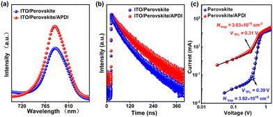
To better capture the performance of the perovskite film without (control) and with (target) APDI treatment, various morphologies and optical characterizations were carried out. Top-view scanning electron microscopy (SEM) showed no particularly significant difference in the grain sizes of the control and target films (Fig. S3, ESI†). However, the contact angle of the control film increased from 57.9° to 76.9° after APDI treatment; this may be due to the presence of alkyl chains in APDI, which increased the hydrophobicity of the film surface (Fig. S4a, ESI†). The UV-vis absorption spectra demonstrated that the target film had better light absorption, which indicated that the APDI modification contributed to improving the quality of the perovskite film without a change in the band-gap (Fig. S4b–d, ESI†). Moreover, the roughness of the perovskite film was reduced from 10.7 nm to 8.19 nm after APDI modification, as observed in the atomic force microscopy (AFM) measurements (Fig. S3c, ESI†). The improved surface roughness means that the perovskite/C60 interface can form better contact, which has the potential to promote efficient charge transport.14 By steady-state (PL) and time-resolved photoluminescence (TRPL), it could be observed that (Fig. 2a) PL intensity of the target film was significantly enhanced than that of the control film, indicating that the APDI can reduce the nonradiative recombination loss of perovskite by the surface passivation and thus is conducive to improving film quality, which agrees with the results observed from UV-vis. The TRPL spectra were fitted by biexponential function (Fig. 2c and Table S2, details are shown in the Characterization, ESI†), and it is found that the average lifetime (τavg) of the target film was prolonged, further confirming the significant passivation effect of APDI.6 Moreover, the defect density of perovskite without and with APDI was quantified by applying the space-charge-limited current (SCLC) method.13 The device structure was ITO/C60/perovskite/with or without APDI/C60/Au (for more details, see the Characterization in ESI†). As shown in Fig. 2c, the calculated Ntrap for the control and target devices were 3.82 × 1015 cm−3 and 3.03 × 1015 cm−3, respectively. This proved that APDI could effectively reduce perovskite defects by surface passivation, which agreed with the analysis of PL/TRPL results.
 | ||
| Fig. 2 (a) PL spectra, (b) TRPL and (c) trap density of perovskite without (control) and with (target) APDI. | ||
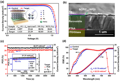
To clarify the effect of ADPI modification on photovoltaic performance (PV), inverted PSCs with the architecture of ITO/PTAA/perovskite/C60/BCP/Ag were fabricated. Schematic diagrams of the device structure and surface passivation of ADPI are shown in Fig. 3a. The cross-sectional SEM (Fig. 3b) image of PSC shows a clear compositional structure with a suitable thickness (∼680 nm) of the perovskite layer.11 For the regulation of perovskite surface properties, the concentration of functional compounds is extremely critical. Here, the optimal concentration of APDI (0.3 mg/ml) was determined by the current density–voltage (J–V) test, as shown in Fig. S5 and Table S3 (ESI†). From Fig. 3a, it can be observed that compared to the PV parameters of the control device (Voc = 1.097 V, Jsc = 22.64 mA cm−2, FF = 80.56%, and PCE = 20.01%), the performance of the target device is significantly enhanced (Voc = 1.121 V, Jsc = 23.29 mA cm−2, FF = 82.03%, and PCE = 21.41%). Additionally, the average values demonstrated improved PV parameters for the target devices (Fig. S6 and Table S4, ESI†). The MPP (power output at the maximum power point) measurements for the control (19.11%) and target (20.53%) devices are shown in Fig. 3c. The steady-state PCE and Jsc of the target devices were higher than those of the control devices, and the values matched with the J–V data. As shown in Fig. 3d, the integrated current (control = 21.75 mA cm−2 and target = 22.33 mA cm−2) from the external quantum efficiency (EQE) agrees with the Jsc values from the J–V curves.
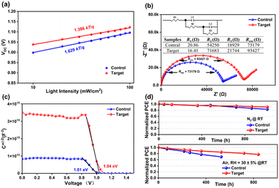
To better understand the charge recombination characteristics of the devices, the Voc and Jscvs. light intensity were studied. The result of Jscvs. light intensity demonstrated (Fig. S7a, ESI†) a fit slope closer to the value of 1 for the target device (αcontrol = 0.962 and αtarget = 0.976), which indicated that, compared to the control device, the target device had lower bimolecular recombination. Fig. 4a shows that the target device had a smaller slope of 1.386 kT/q compared to the pristine one (1.629 kT/q), indicating that the non-radiative charge recombination of the device was suppressed by the surface passivation of APDI. The electrochemical impedance spectroscopy (EIS) showed that the Rs (R1) of the target device was lower than that of the control one, while the Rrec (Rrec = R2 + R3) was higher than the control (Fig. 4b).15 As shown in Fig. S7b (ESI†), the target device also illustrated higher Rrec at different bias voltages than the control, which further affirmed the reduced charge recombination at the perovskite/C60 interface. Furthermore, the Mott–Schottky measurements showed (Fig. 4c) that the target device had a higher built-in potential (Vbi = 1.04 V) than the control one (Vbi = 1.01 V), indicating that there was a stronger charge transfer capability at the interface after APDI treatment.16 To deeply illustrate the charge transport of PSCs at the perovskite/C60 interface, we tested the relationship of photocurrent (Jph) vs. effective applied voltage (Veff), as shown in Fig. S7c (for more details, see the characterization in ESI†), and the results showed that the exciton dissociation probability (Pdiss) value of the target (∼91%) device was higher than that of control (∼89%), which indicates that the APDI-modified interface was more favorable for charge transfer to the electrode, thus promoting the reduction of charge recombination.17
Considering the stability of the PSCs, we investigated the decay of the PV parameters of the devices in different environments. The results showed that the unencapsulated target device maintained 90% and 78% of the initial PCE after aging under nitrogen or air for 1000 h and 800 h, respectively, while the control device had only 81% and 62%, respectively (Fig. 4d). By performing the contact angle test (Fig. S3, ESI†), it was clear that the perovskite/APDI films showed stronger hydrophobicity, which may be due to the effect of alkyl chains on the APDI. Therefore, this largely enhances the stability of the target devices in both air and nitrogen atmospheres. The decay trend of the remaining parameters (Voc, Jsc, FF) is shown in Fig. S8 (ESI†). To further investigate the reason for the degradation of device performance, we examined the variation in XRD parameters during the aging of perovskite films before and after APDI treatment. The results (Fig. S9, ESI†) showed that the pristine perovskite film exhibited a new signal attributed to the PbI2 after being aged for 3 days in the air, indicating that the decomposition of perovskite film may be due to the vulnerability of defect sites on the perovskite surface to erosion by external factors. The erosion process of the target film by external factors was delayed based on the improvement of perovskite film quality, which was caused by the surface termination passivation effect of APDI and the presence of alkyl chains in APDI.18
Overall, we employed an imidazole-based diiodide (APDI) to modulate the terminal environment of the Cs/FA perovskite surface to enhance the inverted PSC performance. Consequently, the APDI-treated device achieved a PCE of 21.41% and exhibited superior stability under air or nitrogen conditions. The reasons for performance enhancement were as follows: (i) the binding of N in APDI and uncoordinated Pb2+, which effectively reduces the defect density and the trap-assisted charge recombination; (ii) the acceleration of the efficient charge transport at the perovskite/C60 interface due to the fine interface properties between perovskite/APDI and C60; (iii) the alkyl chains of APDI can enhance the hydrophobicity of perovskite films, thus beneficially reducing the risk of perovskite film being eroded by H2O. This study demonstrated a featured recipe for improving PSC performance by introducing ammonium salts with bifunctional groups onto the perovskite surface.
This research was supported by the Fundamental Research Funds for the Jiaxing University (No. CD70519019), the Jiaxing Public Welfare Research Project (No. 2022AY10003), the Postdoctoral Science Preferential Funding of Zhejiang Province (No. ZJ2022148) and the Zhejiang Provincial Natural Science Foundation of China (No. LQ23E030005, LGJ22B040001).
Conflicts of interest
There are no conflicts to declare.Notes and references
- A. Kojima, K. Teshima, Y. Shirai and T. Miyasaka, J. Am. Chem. Soc., 2009, 131, 6050–6051 CrossRef CAS PubMed.
- H. Min, D. Y. Lee, J. Kim, G. Kim, K. S. Lee, J. Kim, M. J. Paik, Y. K. Kim, K. S. Kim, M. G. Kim, T. J. Shin and S. I. Seok, Nature, 2021, 598, 444–450 CrossRef CAS.
- X. D. Li, W. X. Zhang, X. M. Guo, C. Y. Lu, J. Y. Wei and J. F. Fang, Science, 2022, 375, 434–437 CrossRef CAS PubMed.
- D. P. McMeekin, G. Sadoughi, W. Rehman, G. E. Eperon, M. Saliba, M. T. Hörantner, A. Haghighirad, N. Sakai, L. Korte, B. Rech, M. B. Johnston, L. M. Herz and H. J. Snaith, Science, 2016, 351, 151–155 CrossRef CAS PubMed.
- D. Y. Luo, W. Q. Yang, Z. P. Wang, A. Sadhanala, Q. Hu, R. Su, R. Shivanna, G. F. Trindade, J. F. Watts, Z. J. Xu, T. H. Liu, K. Chen, F. J. Ye, P. Wu, L. C. Zhao, J. Wu, Y. G. Tu, Y. F. Zhang, X. Y. Yang, W. Zhang, R. H. Friend, Q. H. Gong, H. J. Snaith and R. Zhu, Science, 2018, 360, 1442–1446 CrossRef CAS PubMed.
- F. Z. Li, X. Deng, F. Qi, Z. Li, D. J. Liu, D. Shen, M. C. Qin, S. F. Wu, F. Lin, S.-H. Jang, J. Zhang, X. H. Lu, D. Y. Lei, C.-S. Lee, Z. L. Zhu and A. K.-Y. Jen, J. Am. Chem. Soc., 2020, 142, 20134–20142 CrossRef CAS PubMed.
- S. S. Chen, X. Z. Xu, S. Xu, H. Y. Jiao, L. Zhao and J. S. Huang, Science, 2021, 373, 902–907 CrossRef CAS PubMed.
- Y. Y. Huang, S. N. Li, C. R. Wu, S. Wang, C. Y. Wang and R. X. Ma, Chem. Commun., 2020, 56, 6731–6734 RSC.
- Z. Li, B. Li, X. Wu, S. A. Sheppard, S. Zhang, D. Gao, N. J. Long and Z. Zhu, Science, 2022, 376, 416–420 CrossRef CAS PubMed.
- R. Wang, J. J. Xue, K.-L. Wang, Z.-K. Wang, Y. Q. Luo, D. Fenning, G. W. Xu, S. Nuryyeva1, T. Y. Huang, Y. P. Zhao, J. L. Yang, J. H. Zhu, M. H. Wang, S. Tan, I. Yavuz, K. N. Houk and Y. Yang, Science, 2019, 366, 1509–1513 CrossRef CAS PubMed.
- Z. Xing, M.-W. An, Z.-C. Chen, M. Hu, X. Huang, L.-L. Deng, Q. Zhang, X. Guo, S.-Y. Xie and S. Yang, J. Am. Chem. Soc., 2022, 144, 13839–13850 CrossRef CAS PubMed.
- S. F. Hu, K. Otsuka, R. Murdey, T. Nakamura, M. A. Truong, T. Yamada, T. Handa, K. Matsuda, K. Nakano, A. Sato, K. Marumoto, K. Tajima, Y. Kanemitsu and A. Wakamiya, Energy Environ. Sci., 2022, 15, 2096–2107 RSC.
- L. Yang, J. S. Feng, Z. K. Liu, Y. W. Duan, S. Zhan, S. M. Yang, K. He, Y. Li, Y. W. Zhou, N. Y. Yuan, J. N. Ding and S. Z. Liu, Adv. Mater., 2022, 34, 2201681 CrossRef CAS PubMed.
- P. Chen, Y. Bai, S. C. Wang, M. Q. Lyu, J.-H. Yun and L. Z. Wang, Adv. Funct. Mater., 2018, 28, 1706923 CrossRef.
- Q. Zhou, Y. F. Gao, C. S. Cai, Z. Z. Zhang, J. B. Xu, Z. Y. Yuan and P. Gao, Angew. Chem., Int. Ed., 2021, 60, 8303–8312 CrossRef CAS PubMed.
- Z. H. Fan, Y. Yin, B. Cai, Q. S. Ma, Q. L. Liu, X. H. Liu, Y. H. Lv and W.-H. Zhang, Chem. Sci., 2022, 13, 10512–10522 RSC.
- J.-L. Wu, F.-C. Chen, Y.-S. Hsiao, F.-C. Chien, P. Chen, C.-H. Kuo, M. H. Huang and C.-S. Hsu, ACS Nano, 2011, 5, 959–967 CrossRef CAS PubMed.
- Y. Han, S. Meyer, Y. Dkhissi, K. Weber, J. M. Pringle, U. Bach, L. Spiccia and Y.-B. Cheng, J. Mater. Chem. A, 2015, 3, 8139–8147 RSC.
Footnote |
| † Electronic supplementary information (ESI) available. See DOI: https://doi.org/10.1039/d3cc01379k |
| This journal is © The Royal Society of Chemistry 2023 |


