 Open Access Article
3D hole-transporting materials based on coplanar quinolizino acridine for highly efficient perovskite solar cells†
Mingdao
Zhang
 *ab,
Gang
Wang
c,
Danxia
Zhao
a,
Chengyan
Huang
ad,
Hui
Cao
*a and
Mindong
Chen
*a
aDepartment of Chemistry, Jiangsu Key Laboratory of Atmospheric Environment Monitoring and Pollution Control, School of Environmental Science and Engineering, Nanjing University of Information Science & Technology, Nanjing 210044, Jiangsu, PR China. E-mail: yccaoh@hotmail.com; chenmd@nuist.edu.cn
bDepartment of Macromolecular Science and Engineering, Case Western Reserve University, 10900 Euclid Avenue, Cleveland, OH 44106, USA. E-mail: mxz372@case.edu
cBeijing Institute of Information Technology, Beijing 100094, PR China
dSchool of Chemistry & Life Science, Nanjing University Jinling College, Nanjing 210089, Jiangsu, PR China
First published on 25th September 2017
Abstract
Over the past five years, perovskite solar cells (PSCs) have gained intense worldwide attention in the photovoltaic community due to their low cost and high power conversion efficiencies (PCEs). One of the most significant issues in achieving high PCEs of PSCs is the development of suitable low-cost hole-transporting materials (HTMs). Here, we put forward a new concept of HTMs for PSCs: a 3D structure with a core of coplanar quinolizino acridine, derived from the conventional concept of 2D triphenylamine HTMs. A cheaper Ag nanolayer was utilized to replace Au as the counter electrodes, and the title HTM TDT-OMeTAD was synthesized via an easy four-step synthesis (total yield: 61%) to achieve the low cost and convenient manufacture of PSCs. Compared with the conventional 2D triphenylamine HTM, TTPA-OMeTPA, PSC devices based on the 3D HTM TDT-OMeTPA showed a significant improvement in PCE from 10.8% to 16.4%, even outperforming Spiro-OMeTAD (14.8%). TDT-OMeTAD’s highest PCE mainly results from it having the highest open-circuit voltage (Voc) of 1.01 V in this work, which is proven to be due to the higher hole mobility, matching energy levels, higher hydrophobicity and the smaller dark current. Moreover, an incident photon–current conversion efficiency (IPCE) test and time-resolved photoluminescence (TRPL) have been carried out to observe the better hole injecting efficiency and photoelectric conversion capability of TDT-OMeTPA based PSCs than Spiro-OMeTAD. The TDT-OMeTPA based PSCs exhibited >75% reproducibility (PCE > 15%) and retained 93.2% of the initial PCE after >500 hours.
Introduction
In recent decades, solar photovoltaic power generation has become an effective way to solve environmental and energy issues. With the development of photovoltaics, the type of solar cell developed from the traditional crystalline silicon cell into all kinds of new solar cells. Organic–inorganic metal halide perovskite solar cells (PSCs) have received significant attention due to their simple manufacturing, low cost and high power conversion efficiency (PCE).1–4 Typically, a perovskite solar cell has a sandwiched structure: FTO glass/TiO2 layer/perovskite/hole transporting materials (HTMs)/Ag or Au. Since 2009, the power conversion efficiency (PCE) of PSCs has been improved from 3.9% to above 20%.5,6 Organic HTMs as interfacial contact materials, which extract holes from the perovskite layer and transport them to the anode, are significant for the further improvement of the performance of PSCs. To date, most of the high-performance PSCs reported so far utilize 2,2,7,7-tetrakis(N,N-di-p-methoxy-phenyl-amine)-9,9-spirobifluorene (Spiro-OMeTAD) and its derivatives as HTMs.7–11 Although significant development of PSCs has been achieved, there are also many issues such as the relatively high cost, mismatched energy levels, the complicated doping protocol and limited long-term stability, which need to be addressed to develop PSC technology for real practical applications.8In this regard, it is meaningful to develop new HTMs for the further enhancement of the device efficiency and stability of PSCs, as well as to investigate their structure–property relationships. Many different types of HTM, such as triphenylamine,12 carbazoles,13 acene derivatives,14 phenoxazines,15 triazatruxene16 and azomethine,17 have been developed and utilized in PSCs. Previous research proved that many factors, such as hole mobility, energy levels, perovskite surface passivation, the hydrophobicity of the surface, and so on, should be considered when designing new HTMs.18–20 However, it is a huge challenge to integrate all these significant factors into one single HTM.20
Herein, we report a new HTM that incorporates the following factors: a low cost and easy synthesis, a high hole mobility, matched energy levels, a hydrophobic surface and perovskite surface passivation. The title HTM, TDT-OMeTPA, has a co-planar quinolizino acridine21 as a core unit (part A, blue in Fig. 1a), which is conjugated with three 4,4′-dimethoxydiphenylamine groups (part B, pink in Fig. 1a) surrounded by six 4-methylphenyl groups (part C, green in Fig. 1a). The planar, rigid and fully conjugated molecular geometries between parts A and B allow TDT-OMeTPA to have a high hole mobility, suitable surface energy and matching energy levels. Moreover, part C constructs the 3D structure, which helps restrain molecule aggregation and back hole-transfer at the interface of the HTM with the perovskite. A simple HTM, TTPA-OMeTPA, with triphenylamine as a core unit was utilized as a reference HTM (Fig. 1b).22 As a result, PSCs using TDT-OMeTPA as the hole-transporting layer show a high PCE of 16.4% (10.8% and 14.8% for TTPA-OMeTPA and Spiro-OMeTAD respectively) under AM 1.5G illumination, which is one of the highest values reported so far for PSC devices employing triphenylamine HTMs.
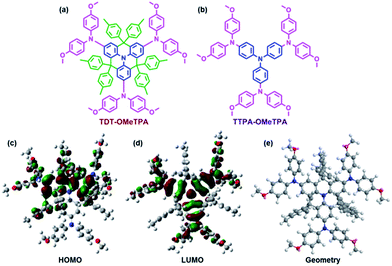 | ||
| Fig. 1 Molecular structures of (a) TDT-OMeTPA and (b) TTPA-OMeTPA. The (c) HOMO, (d) LUMO and (e) optimized molecular conformation of TDT-OMeTPA obtained from DFT calculations. | ||
Results and discussion
The synthetic routes of TDT-OMeTPA and TTPA-OMeTPA are respectively shown in Fig. S1 and S2 (ESI†).23 The total yield of the four-step synthesis of TDT-OMeTAD is 61%. TTPA-OMeTPA was prepared via a straightforward one-step condensation synthesis. The two triphenylamine derivatives were purified by column chromatography followed by recrystallization and characterization (1H NMR, see the ESI†) and the analytical data were consistent with the proposed structures.To investigate the electronic and geometric structures of TDT-OMeTPA and TTPA-OMeTPA, the molecular orbitals (MOs) of the two HTMs were calculated using density functional theory (DFT) at the B3LYP/6-31G(d) level. Fig. 1b and c show the highest occupied and the lowest unoccupied MOs, the HOMO and LUMO, respectively. The electron densities of TDT-OMeTPA (Fig. 1c and d) and TTPA-OMeTPA (Fig. S3, ESI†) are delocalized within the conjugated moieties of the whole molecules. The methoxy groups of TDT-OMeTPA and TTPA-OMeTPA with oxygen lone-pairs face outward from the triphenylamine core. It has been demonstrated that Lewis basic heteroatoms can potentially passivate a perovskite surface, i.e. by coordinating with lead ions via halide vacancies.24–26 Also, compared with TTPA-OMeTPA, the coplanar rigid molecule structure enables TDT-OMeTPA to have a stronger conjugation and more ordered assemblies for better hole transport in the film state. Meanwhile, compared to the 2D structure of TTPA-OMeTPA (Fig. S4, ESI†), six 4-hexylphenyl groups around the coplanar triphenylamine moiety arranged in different directions shape TDT-OMeTPA as a 3D molecule, restraining molecule accumulation and charge recombination (Fig. 1e and S5, ESI†).
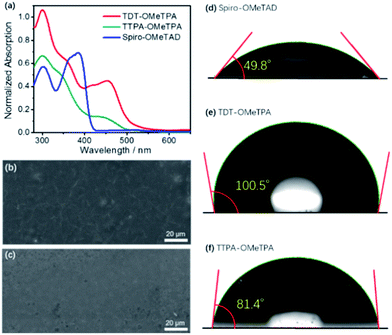
The normalized absorption spectra and photoluminescence (PL) spectra of TDT-OMeTPA, TTPA-OMeTPA and Spiro-OMeTAD in CH2Cl2 solution are shown in Fig. 2a and S6 (ESI†). All three HTMs display strong absorption peaks around 300–370 nm. TTPA-OMeTPA shows a lower absorption energy at 400–470 nm compared to TDT-OMeTPA. TDT-OMeTPA displays a wide light-harvesting ability in the visible light region resulting in a strong ionization capacity, and the ionic intermediates formed from TDT-OMeTPA will be more stable, indicating a high efficiency of receiving and transferring holes. Compared with Spiro-OMeTAD, TDT-OMeTPA has much larger Stokes shifts, which are beneficial for enhancing the hole-extracting efficiency in solar cells.2,3 The intersection wavelengths for TDT-OMeTPA and TTPA-OMeTPA are 452 and 458 nm, corresponding to an Eg of 2.74 and 2.71 eV, respectively. Fig. 2b and c and S7 (ESI†) respectively show the SEM images of the TDT-OMeTPA, TTPA-OMeTPA and Spiro-OMeTAD layers accumulated on perovskite layers. The TDT-OMeTPA HTM layer (Fig. 2b) is as compact as the Spiro-OMeTAD layer (Fig. S7, ESI†). However, the TTPA-OMeTPA layer has obvious round holes and defects with an average diameter of 1.5 μm (Fig. 2c), which may result in the degradation of the PSC performance.
In addition to compactness, the surface wettability of the HTM layer also significantly affects the device performance. Recent reports demonstrated that a relatively hydrophobic surface would help keep the perovskite layer completely free from water.8–10 For TDT-OMeTPA, in addition to its coplanar triphenylamine, the six 4-methylphenyl moieties can modulate the HTM surface energy, i.e. at the solid/gas interface. This is quite different from TTPA-OMeTPA and Spiro-OMeTAD without 4-methylphenyl moieties. As shown in Fig. 2d–f, water contact angle tests were carried out. Spiro-OMeTAD and TTPA-OMeTPA exhibit contact angles of 49.8° and 81.4° to water droplets, respectively (Fig. 2d and f). In sharp contrast, TDT-OMeTPA exhibits a much larger contact angle of 100.5° (Fig. 2e).
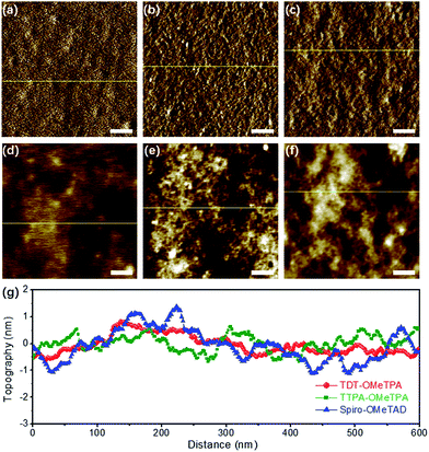
The surface morphology of the HTM layers was further studied using tapping mode atomic force microscopy (AFM) (Fig. 3). The AFM amplitude and AFM height images (Fig. 3a and d) demonstrated the smoother morphology of the TDT-OMeTPA HTM layer than that of the TTPA-OMeTPA (Fig. 3b and e) and Spiro-OMeTAD (Fig. 3c and f) layers. Meanwhile, the root-mean-square (RMS) roughness of the TDT-OMeTPA HTM layer (1.5 nm) is much smaller than that of the Spiro-OMeTAD layer (2.3 nm), as indicated by the topography line profiles (Fig. 3g). Line profiles of the AFM amplitude images show a similar trend (Fig. S8, ESI†). Such hydrophobicity and smooth morphology of the TDT-OMeTPA HTM layer are beneficial to obtain high-quality PSC devices.9,10
The glass transition temperatures (Tg) of TDT-OMeTPA, TTPA-OMeTPA and Spiro-OMeTAD were investigated by differential scanning calorimetry (DSC) under an argon atmosphere (Fig. S9, ESI†). As reported,22 no glass transition was observed in the range of 25–200 °C for TTPA-OMeTPA. The Tg of TDT-OMeTPA (169 °C) was higher than that of Spiro-OMeTAD (122 °C). A higher Tg value indicates a more stable amorphous state, which is beneficial to the PSC device stability.28
To investigate the hole-transporting abilities, the hole mobility values of TDT-OMeTPA, TTPA-OMeTPA and Spiro-OMeTAD were measured using a space-charge limited current (SCLC) method (Fig. S10, ESI†) according to the Mott–Gurney law.27,28 The hole mobility of TDT-OMeTPA (1.4 × 10⁻⁴ cm2 (V s)−1) is higher than those of Spiro-OMeTAD (9.1 × 10⁻⁵ cm2 (V s)−1) and TTPA-OMeTPA (7.3 × 10⁻⁶ cm2 (V s)−1). The hole mobility of Spiro-OMeTAD is close to the reported values,29,30 demonstrating the reliability of the SCLC method. Compared with TTPA-OMeTPA, the two orders of magnitude higher hole mobility of TDT-OMeTPA proves that the new design of the HTM (a 3D structure with a core of coplanar quinolizino acridine) is highly effective in improving the hole-transporting ability. The hole mobilities and the PCEs of TDT-OMeTPA, TTPA-OMeTPA and Spiro-OMeTAD exhibit a correlation (see below), indicating the critical significance of a high hole mobility of HTMs for the overall performance.31
The experimental HOMO energy levels of TDT-OMeTPA and TTPA-OMeTPA were derived from the ground-state oxidation potential ES+/S obtained using cyclic voltammetry (CV). The CV curves of Spiro-OMeTAD, TDT-OMeTPA and TTPA-OMeTPA in DMF with 0.1 M tetrabutylammonium hexafluorophosphate (TBAPF6) are presented in Fig. S11 (ESI†). The pair of redox peaks of the three HTMs are highly reversible, suggesting their excellent electrochemical stability.4,9,10 TDT-OMeTPA and TTPA-OMeTPA exhibited onset oxidation potentials (Eox,onset) at 0.68 V and 0.60 V (vs. Ag/Ag+), respectively. The HOMO levels of TDT-OMeTPA and TTPA-OMeTPA were calculated according to eqn (1):
| ES+/S = −(Eox,onset + 4.80 − φFc/Fc+) [eV] | (1) |
As expected, TDT-OMeTPA (−5.28 eV) has a deeper HOMO level than those of TTPA-OMeTPA (−5.20 eV) and Spiro-OMeTAD (−5.22 eV), which can effectively facilitate hole transportation in TDT-OMeTPA-based PSC devices (Table 1 and Fig. 4a and S12†).9,10 Meanwhile, the experimental LUMO level ES+/S* (calculated from the HOMO levels and Eg) of TDT-OMeTPA (−2.54 eV) is the lowest among the three HTMs. All the data are listed in Table 1.
| HTM | λ em (nm) | E S+/S (eV) | E g (V) | E S+/S* (eV) | E S+/S (eV) | E S+/S* (eV) |
|---|---|---|---|---|---|---|
| a Measured in DCM solution. b Measured in DMF/tetrabutylammonium hexafluorophosphate (TBAPF6) (0.1 M) solution, using a glassy carbon working electrode, Ag/AgCl reference electrode and Pt counter electrode with Fc/Fc+ as an internal standard. c Estimated from the intersection of the normalized absorbance and emission spectra. d Calculated from ES+/S* = ES+/S + Eg. e Ground- and excited-state TD-DFT calculations were done at the B3LYP/6-31G(d) level. | ||||||
| TDT-OMeTAD | 452 | −5.28 | 2.74 | −2.54 | −4.98 | −1.34 |
| TTPA-OMeTPA | 458 | −5.20 | 2.71 | −2.49 | −5.04 | −1.42 |
| Spiro-OMeTAD | 409 | −5.22 | 3.03 | −2.19 | −5.22 | −1.64 |
The energy level diagram of the HTMs, with both DFT calculated and experimental values, is depicted in Fig. S12 (ESI†). The HOMO level of a double-mixed perovskite is at −5.65 eV (vs. vacuum)32 indicating that TDT-OMeTPA, TTPA-OMeTPA and Spiro-OMeTAD all have enough overpotential to facilitate efficient hole extraction from the perovskite to the HTM. Moreover, the HOMO level of TDT-OMeTPA is more stabilized than that of TTPA-OMeTPA, and is even more reasonable compared to that of Spiro-OMeTAD (ES+/S = −5.22 eV vs. vacuum),33 thus leading a higher open-circuit voltage (Voc).
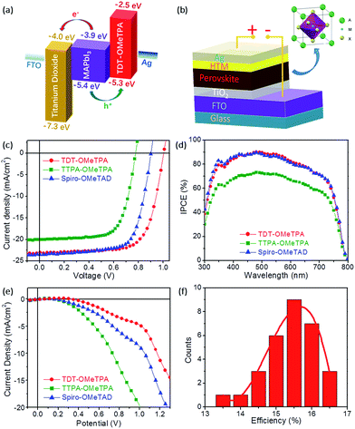
The PSC device structure is FTO/TiO2/perovskite (CH3NH3PbI3)/HTM/Ag in this work (Fig. 4b). The current–voltage (J–V) characteristics of the CH3NH3PbI3 based solar cell measured under simulated solar illumination (AM 1.5G 100 mW cm−2) are shown in Fig. 4c, and the corresponding photovoltaic parameters are summarized in Table 2. The cells fabricated with TDT-OMeTPA displayed the highest power conversion efficiency (PCE) of 16.4% with a short-circuit current density (Jsc) of 23.1 mA cm−2, open circuit voltage (Voc) of 1.01 V and a fill factor (FF) of 70.4. The device using TTPA-OMeTPA exhibited a smaller η value of 10.8% due to the smaller Voc and Jsc values (Voc = 0.776 V, Jsc = 20.1 mA cm−2 and FF = 69.3). A higher Voc results in the higher PCE of the device with TDT-OMeTPA compared with those of Spiro-OMeTAD and TTPA-OMeTPA, which is proven to be due to the higher hole mobility, matching energy levels, higher hydrophobicity and the smaller dark current of TDT-OMeTPA.3,11
| HTM | J sc (mA cm−2) | V oc (V) | FF (%) | η (%) |
|---|---|---|---|---|
| TDT-OMeTPA | 23.1 | 1.01 | 70.4 | 16.4 |
| TTPA-OMeTPA | 20.1 | 0.776 | 69.3 | 10.8 |
| Spiro-OMeTAD | 23.3 | 0.902 | 70.2 | 14.8 |
Fig. 4d shows the incident-photon-to-current conversion efficiency (IPCE) as a function of excitation wavelength. The IPCE curves of the three HTMs have similar profiles with maxima at 480 nm due to having the same light-harvesting perovskite layers. Compared with those with TTPA-OMeTPA, devices with TDT-OMeTPA and Spiro-OMeTAD display higher IPCE values across the whole visible wavelength range, maintaining a value of 70% from 350 nm to 700 nm, with the PSCs harvesting light up to 800 nm, demonstrating the effectiveness of the 3D coplanar triphenylamine for improving visible light-harvesting, leading to a high short-circuit photocurrent (Jsc). This result is consistent with the results of the J–V tests.
In addition to the HOMO–LUMO level and absorption band, the dark current may also seriously affect the photovoltaic performance of PSCs (Fig. 4e).34 The dark current of the TDT-OMeTPA based PSC is smaller than that of the Spiro-OMeTAD based PSC, while the TTPA-OMeTPA based PSC exhibits a much higher dark current than that of the Spiro-OMeTAD based PSC. The dark current values of the PSCs based on TDT-OMeTPA, TTPA-OMeTPA and Spiro-OMeTAD are −4.72, −19.38 and −8.61 mA cm−2, respectively, under a potential of 1.0 V. The trend is consistent with the Voc values (Table 2). Therefore, the dark current is a noticeable factor affecting the photovoltaic performance of the PSCs in this work.
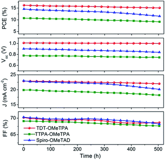
The good reproducibility is also investigated for PSCs using the TDT-OMeTPA HTM. The efficiency histogram in Fig. 4f shows that >75% of the devices (among 30 devices) have a PCE higher than 15%, demonstrating the excellent reproducibility of the TDT-OMeTPA based PSC device. The durability of the photovoltaic performance of the PSCs based on TDT-OMeTPA, TTPA-OMeTPA and Spiro-OMeTAD was further investigated under simulated 1.5G full sunlight (Fig. 5). The performance of the PSCs based on the three HTMs decreased very slowly in the first 10 days. After aging under one sun illumination for >500 hours, the TDT-OMeTPA, TTPA-OMeTPA and Spiro-OMeTAD based devices respectively retained 93%, 84% and 79% of their initial PCEs. The decrease of FF and Jsc after 300 hours was the main contribution to the reductions in the PCEs, especially for that of Spiro-OMeTAD. The much better stability of the TDT-OMeTPA based PSC compared with the Spiro-OMeTAD and TTPA-OMeTPA based PSCs may be partly attributed to the more hydrophobic nature of TDT-OMeTPA, as demonstrated by the contact angles (Fig. 2d–f).29
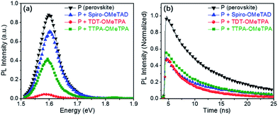
In order to determine the capability of the new HTMs as hole acceptors in the perovskite-based devices, we recorded time-integrated photoluminescence (TIPL) on the perovskite films (Fig. 6a). Upon exciting the bare perovskite films at 420 nm, strong TIPL appears in the TIPL spectra between 1.58 and 1.63 eV. After accumulating the different HTM layers, the TIPL spectra are blue-shifted, where the optical properties of the HTMs and the intense chemical interaction between the perovskite and the HTM could have an impact on the perovskite interface nature. Furthermore, the TIPL intensity of the perovskite films containing the different HTMs is relatively reduced, indicating that the holes can be effectively injected into the HOMO of the HTM from the valence band of the perovskite.35
To further illustrate the injection rates of holes, we further studied the decay dynamics through time-resolved photo-luminescence (TRPL) (Fig. 6b). The emission lifetime for the perovskite films containing the different HTMs was investigated using a two-component exponential decay model, as shown in Table 3. The pristine perovskite films showed the longest charge carrier life time (τ2 = 17 ns). With the hole injection from the perovskite to the HTM, the TRPL decay is obviously accelerated when the HTM is present in the device.9,10,21 The hole injection from the valence band of the perovskite into the HOMOs of TDT-OMeTPA is close to that of Spiro-OMeTAD but is more efficient than that of TTPA-OMeTPA, indicating the sufficiently fast charge regeneration in TDT-OMeTPA based PSCs. In other words, the hole injection from the valence band of the perovskite into the HOMO of TDT-OMeTPA is relatively more efficient compared to that of TTPA-OMeTPA.11,26,33
| Sample | A1 | Life time τ1 (ns) | A2 | Life time τ2 (ns) |
|---|---|---|---|---|
| P (perovskite) | 22 | 4.5 | 78 | 17 |
| P + TDT-OMeTPA | 50 | 3.4 | 50 | 11 |
| P + TTPA-OMeTPA | 32 | 4.0 | 68 | 13 |
| P + Spiro-OMeTAD | 16 | 2.4 | 84 | 10 |
Conclusions
In summary, we developed a new 3D HTM, TDT-OMeTPA, with coplanar quinolizino acridine as the core, via structure modification of the conventional HTM, TTPA-OMeTPA, with a regular triphenylamine-core. The hole mobility of TDT-OMeTPA is 50 times higher than that of TTPA-OMeTPA. The PSC fabrication and characterization demonstrated the huge improvement of PCE from the PSC based on TTPA-OMeTPA (10.8%) to that based on TDT-OMeTPA (16.4%), even outperforming the PSC based on Spiro-OMeTAD (14.8%) and demonstrating the advantage of the novel 3D triphenylamine moiety. The SEM, contact angle and AFM results indicate the smooth morphology and high quality of the TDT-OMeTAD HTM layer. From the DFT (TD-DFT) calculations, CV measurements and UV-vis and PL spectra, the HOMO and LUMO energy levels of TDT-OMeTPA were found to be well matched to the energy levels of the perovskite material. Furthermore, the most efficient HTM, TDT-OMeTPA, had the highest open circuit voltage (Voc = 1.01 V) because the HOMO level is more compatible with the perovskite. This study demonstrates the advantages of the new type of HTM for PSCs: a 3D structure with a core of coplanar quinolizino.Experimental
Syntheses of TDT-OMeTPA and TTPA-OMeTPA
Fig. 1a, S1 and S2† illustrate the synthetic routes of TDT-OMeTPA and TTPA-OMeTPA. Compound 3 was synthesized by reported procedures.23 The first three steps of the synthesis of TDT-OMeTAD are described in the ESI† and compounds 3 and 4 are characterized by 1H NMR in Fig. S13 and S14 (ESI†).Solar cell fabrication and characterization
The FTO (F-doped SnO2, Pilkington, TEC8) glasses were cleaned in an ultrasonic bath with detergents, acetone, and deionized water respectively for 30 min, and then a blocking layer of TiO2 (60 nm, bl-TiO2) was deposited onto the FTO glass by spray pyrolysis using a 20 mM titanium diisopropoxide bis(acetylacetonate) solution (Aldrich) at 450 °C. A mesoporous TiO2 layer was spin-coated on the top of the bl-TiO2/FTO substrate at 1000 rpm for 60 s using a TiO2 (∼50 nm particle size) paste. The pristine TiO2 paste was diluted in 2-methoxyethanol (1 g/5 mL). The mesoporous TiO2 layer was annealed at 550 °C for 30 min in air, which led to a thickness of about 100 nm. These substrates were further treated with 40 mM TiCl4 aqueous solution for 30 min at 70 °C, followed by rinsing with deionized water and ethanol and vacuum drying (overnight). The (FAPbI3)0.92(MAPbBr3)0.08 perovskite solution (with a small excess of PbI2) was coated onto the mp-TiO2/bl-TiO2/FTO substrate (70 °C) by two consecutive spin-coating steps at 1000 and 4000 rpm for 5 s and 10 s, respectively. During the second spin-coating step, 0.5 mL ethyl ether was poured onto the substrate. The 1.05 M solution for the (FAPbI3)0.92(MAPbBr3)0.08 perovskite was prepared by dissolving FAI (NH2CH![[double bond, length as m-dash]](https://www.rsc.org/images/entities/char_e001.gif) NH2I) and MABr (CH3NH3Br) with PbI2 and PbBr2 in DMF (N,N-dimethylformamide) and DMSO (dimethylsulfoxide) (6
NH2I) and MABr (CH3NH3Br) with PbI2 and PbBr2 in DMF (N,N-dimethylformamide) and DMSO (dimethylsulfoxide) (6![[thin space (1/6-em)]](https://www.rsc.org/images/entities/char_2009.gif) :
:![[thin space (1/6-em)]](https://www.rsc.org/images/entities/char_2009.gif) 1 v/v). The perovskite-deposited substrate was then dried on a hot plate at 100 °C for 10 min. TTPA-OMeTPA, TDT-OMeTAD and Spiro-OMeTAD were spin-coated at 4000 rpm for 60 s from a chlorobenzene solution (68 mmol L−1) containing Li-TFSI (Li-bis(trifluoromethanesulfonyl) imide, 9 mmol L−1) and TBP (tert-butylpyridine, 55 mmol L−1) as dopants. Finally, a 120 nm Ag electrode was deposited by thermal evaporation under a high vacuum.
1 v/v). The perovskite-deposited substrate was then dried on a hot plate at 100 °C for 10 min. TTPA-OMeTPA, TDT-OMeTAD and Spiro-OMeTAD were spin-coated at 4000 rpm for 60 s from a chlorobenzene solution (68 mmol L−1) containing Li-TFSI (Li-bis(trifluoromethanesulfonyl) imide, 9 mmol L−1) and TBP (tert-butylpyridine, 55 mmol L−1) as dopants. Finally, a 120 nm Ag electrode was deposited by thermal evaporation under a high vacuum.
A Keithley 2400 source meter and a Newport 3A monochromator were used for the J–V characterization of the PSCs. The J–V curves of all the devices were measured by masking the active area with a metal mask with an area of 0.085 cm2. The photocurrent action spectra (IPCE vs. wavelength) were measured with an incident photon–current conversion efficiency (IPCE) test system. The modulation frequency was about 2 Hz and the light source from a 300 W xenon lamp (Oriel 6258) was focused on a computer-controlled monochromator (Cornerstone 260 Oriel 74125) to select a single wavelength with a resolution of 10 nm. An NREL traceable Si detector (Oriel 71030NS) was applied to measure the light intensities and an optical power meter (Oriel 70310) was employed to measure the short circuit currents of the PSC devices.
Time-resolved photoluminescence measurements
A device configuration of glass/perovskite/HTM was used in the measurement of photoluminescence (PL) and time-resolved photoluminescence (TR-PL) using a Fluo Time 300. An excitation wavelength of 600 nm was employed during PL measurement. The light was induced at the side of the glass.Density functional theory (DFT) calculations
All calculations were performed using the Gaussian09 program package.36 Density functional theory (DFT) calculations34 were utilized to optimize the ground-state geometry of NUIST1 with the Lee–Yang–Parr function37,38 (B3LYP), and the 6-31G basis set was used for all atoms.39 The time-dependent density functional theory (TD-DFT) calculation40,41 was used in calculating the electronic transitions based on the optimized ground-state structure.Hole mobility measurements
The hole-only devices of TDT-OMeTPA, TTPA-OMeTPA and Spiro-OMeTAD with the structure ITO/PEDOT:PSS/HTM/Ag (ITO = indium tin oxide, PEDOT:PSS = poly(3,4-ethylenedioxythiophene):polystyrene sulfonate) were fabricated to test the hole mobility values of the HTMs. The current density–voltage curves were recorded with a Keithley 2400 source. The thicknesses of the HTM layers are around 100–200 nm and the hole mobility values were calculated using the Mott–Gurney law.27–30Conflicts of interest
There are no conflicts to declare.Acknowledgements
This work was supported by grants from the Natural Science Foundation of China (no. 21401107, 21473092 and 21577065), the International ST Cooperation Program of China (2014DFA90780), the Natural Science Foundation of Jiangsu, China (BK20140986) and the Jiangsu Specially-Appointed Professor Program (R2013T08). Meanwhile, this work was supported by a project funded by the Priority Academic Program Development of Jiangsu Higher Education Institutions (PAPD), China Scholarship Council (201508320148), and the Jiangsu Engineering Technology Research Center of Environmental Cleaning Materials.Notes and references
- I. Cho, N. J. Jeon, O. K. Kwon, D. W. Kim, E. H. Jung, J. H. Noh, J. Seo, S. I. Seok and S. Y. Park, Chem. Sci., 2017, 8, 734–741 RSC.
- M. A. Green, A. Ho-Baillie and H. J. Snaith, Nat. Photonics, 2014, 8, 506–514 CrossRef CAS.
- L. Meng, J. B. You, T. F. Guo and Y. Yang, Acc. Chem. Res., 2016, 49, 155–165 CrossRef CAS PubMed.
- S. Paek, I. Zimmermann, P. Gao, P. Gratia, K. Rakstys, G. Grancini, M. K. Nazeeruddin, M. A. Rub, S. A. Kosa, K. A. Alamry and A. M. Asiri, Chem. Sci., 2016, 7, 6068–6075 RSC.
- D. Q. Bi, W. Tress, M. I. Dar, P. Gao, J. S. Luo, C. Renevier, K. Schenk, A. Abate, F. Giordano, J. P. C. Baena, J. D. Decoppet, S. M. Zakeeruddin, M. K. Nazeeruddin, M. Gratzel and A. Hagfeldt, Sci. Adv., 2016, 2, e1501170 Search PubMed.
- W. S. Yang, J. H. Noh, N. J. Jeon, Y. C. Kim, S. Ryu, J. Seo and S. I. Seok, Science, 2015, 348, 1234–1237 CrossRef CAS PubMed.
- M. Z. Liu, M. B. Johnston and H. J. Snaith, Nature, 2013, 501, 395 CrossRef CAS PubMed.
- B. Xu, D. Q. Bi, Y. Hua, P. Liu, M. Cheng, M. Gratzel, L. Kloo, A. Hagfeldt and L. C. Sun, Energy Environ. Sci., 2016, 9, 873–877 CAS.
- E. T. Hoke, D. J. Slotcavage, E. R. Dohner, A. R. Bowring, H. I. Karunadasa and M. D. McGehee, Chem. Sci., 2015, 6, 613–617 RSC.
- M. E. F. Bouduban, A. Burgos-Caminal, R. Ossola, J. Teuscher and J. E. Moser, Chem. Sci., 2017, 8, 4371–4380 RSC.
- Z. H. Bakr, Q. Wali, A. Fakharuddin, L. Schmidt-Mende, T. M. Brown and R. Jose, Nano Energy, 2017, 34, 271–305 CrossRef CAS.
- S. T. Lv, Y. K. Song, J. Y. Xiao, L. F. Zhu, J. J. Shi, H. Y. Wei, Y. Z. Xu, J. Dong, X. Xu, S. R. Wang, Y. Xiao, Y. H. Luo, D. M. Li, X. G. Li and Q. B. Meng, Electrochim. Acta, 2015, 182, 733–741 CrossRef CAS.
- S. Do Sung, M. S. Kang, I. T. Choi, H. M. Kim, H. Kim, M. Hong, H. K. Kim and W. I. Lee, Chem. Commun., 2014, 50, 14161–14163 RSC.
- S. Kazim, F. J. Ramos, P. Gao, M. K. Nazeeruddin, M. Gratzel and S. Ahmad, Energy Environ. Sci., 2015, 8, 1816–1823 CAS.
- M. Cheng, B. Xu, C. Chen, X. C. Yang, F. G. Zhang, Q. Tan, Y. Hua, L. Kloo and L. C. Sun, Adv. Energy Mater., 2015, 5, 1401720 CrossRef.
- F. J. Ramos, K. Rakstys, S. Kazim, M. Gratzel, M. K. Nazeeruddin and S. Ahmad, RSC Adv., 2015, 5, 53426–53432 RSC.
- M. L. Petrus, T. Bein, T. J. Dingemans and P. Docampo, J. Mater. Chem. A, 2015, 3, 12159–12162 CAS.
- J. J. Wang, S. R. Wang, X. G. Li, L. F. Zhu, Q. B. Meng, Y. Xiao and D. M. Li, Chem. Commun., 2014, 50, 5829–5832 RSC.
- T. Krishnamoorthy, K. W. Fu, P. P. Boix, H. R. Li, T. M. Koh, W. L. Leong, S. Powar, A. Grimsdale, M. Gratzel, N. Mathews and S. G. Mhaisalkar, J. Mater. Chem. A, 2014, 2, 6305–6309 CAS.
- H. Choi, S. Paek, N. Lim, Y. H. Lee, M. K. Nazeeruddin and J. Ko, Chem.–Eur. J., 2014, 20, 10894–10899 CrossRef CAS PubMed.
- P. Qin, S. Paek, M. I. Dar, N. Pellet, J. Ko, M. Gratzel and M. K. Nazeeruddin, J. Am. Chem. Soc., 2014, 136, 8516–8519 CrossRef CAS PubMed.
- T. T. Bui, L. Beouch, X. Sallenave and F. Goubard, Tetrahedron Lett., 2013, 54, 4277–4280 CrossRef CAS.
- Z. Q. Jiang, Y. H. Chen, C. L. Yang, Y. Cao, Y. T. Tao, J. G. Qin and D. G. Ma, Org. Lett., 2009, 11, 1503–1506 CrossRef CAS PubMed.
- J. Cao, Y. M. Liu, X. J. Jing, J. Yin, J. Li, B. Xu, Y. Z. Tan and N. F. Zheng, J. Am. Chem. Soc., 2015, 137, 10914–10917 CrossRef CAS PubMed.
- D. W. deQuilettes, S. M. Vorpahl, S. D. Stranks, H. Nagaoka, G. E. Eperon, M. E. Ziffer, H. J. Snaith and D. S. Ginger, Science, 2015, 348, 683–686 CrossRef CAS PubMed.
- Y. H. Kim, H. Cho, J. H. Heo, T. S. Kim, N. Myoung, C. L. Lee, S. H. Im and T. W. Lee, Adv. Mater., 2015, 27, 1248–1254 CrossRef CAS PubMed.
- D. Poplavskyy and J. Nelson, J. Appl. Phys., 2003, 93, 341–346 CrossRef CAS.
- C. Steck, M. Franckevicius, S. M. Zakeeruddin, A. Mishra, P. Bauerle and M. Gratzel, J. Mater. Chem. A, 2015, 3, 17738–17746 CAS.
- C. Y. Huang, W. F. Fu, C. Z. Li, Z. Q. Zhang, W. M. Qiu, M. M. Shi, P. Heremans, A. K. Y. Jen and H. Z. Chen, J. Am. Chem. Soc., 2016, 138, 2528–2531 CrossRef CAS PubMed.
- I. Yavuz and K. N. Houk, J. Phys. Chem. C, 2017, 121, 993–999 CAS.
- H. Nishimura, N. Ishida, A. Shimazaki, A. Wakamiya, A. Saeki, L. T. Scott and Y. Murata, J. Am. Chem. Soc., 2015, 137, 15656–15659 CrossRef CAS PubMed.
- J. P. C. Baena, L. Steier, W. Tress, M. Saliba, S. Neutzner, T. Matsui, F. Giordano, T. J. Jacobsson, A. R. S. Kandada, S. M. Zakeeruddin, A. Petrozza, A. Abate, M. K. Nazeeruddin, M. Gratzel and A. Hagfeldt, Energy Environ.Sci., 2015, 8, 2928–2934 Search PubMed.
- S. Kazim, M. K. Nazeeruddin, M. Gratzel and S. Ahmad, Angew. Chem., Int. Ed., 2014, 53, 2812–2824 CrossRef CAS PubMed.
- W. Kohn and L. J. Sham, Phys. Rev., 1965, 140, 1133 CrossRef.
- G. C. Xing, N. Mathews, S. Y. Sun, S. S. Lim, Y. M. Lam, M. Gratzel, S. Mhaisalkar and T. C. Sum, Science, 2013, 342, 344–347 CrossRef CAS PubMed.
- G. W. T. M. J. Frisch, H. B. Schlegel, G. E. Scuseria, M. A. Robb, J. R. Cheeseman, G. Scalmani, V. Barone, B. Mennucci, G. A. Petersson, H. Nakatsuji, M. Caricato, X. Li, H. P. Hratchian, A. F. Izmaylov, J. Bloino, G. Zheng, J. L. Sonnenberg, M. Hada, M. Ehara, K. Toyota, R. Fukuda, J. Hasegawa, M. Ishida, T. Nakajima, Y. Honda, O. Kitao, H. Nakai, T. Vreven, J. A. Montgomery Jr, J. E. Peralta, F. Ogliaro, M. Bearpark, J. J. Heyd, E. Brothers, K. N. Kudin, V. N. Staroverov, T. Keith, R. Kobayashi, J. Normand, K. Raghavachari, A. Rendell, J. C. Burant, S. S. Iyengar, J. Tomasi, M. Cossi, N. Rega, J. M. Millam, M. Klene, J. E. Knox, J. B. Cross, V. Bakken, C. Adamo, J. Jaramillo, R. Gomperts, R. E. Stratmann, O. Yazyev, A. J. Austin, R. Cammi, C. Pomelli, J. W. Ochterski, R. L. Martin, K. Morokuma, V. G. Zakrzewski, G. A. Voth, P. Salvador, J. J. Dannenberg, S. Dapprich, A. D. Daniels, O. Farkas, J. B. Foresman, J. V. Ortiz, J. Cioslowski and D. J. Fox, Gaussian 09 Revision B. 01, Gaussian, Inc, Wallingford, CT, 2010 Search PubMed.
- A. D. Becke, Phys. Rev. A, 1988, 38, 3098–3100 CrossRef CAS.
- C. T. Lee, W. T. Yang and R. G. Parr, Phys. Rev. B: Condens. Matter Mater. Phys., 1988, 37, 785–789 CrossRef CAS.
- P. J. Hay and W. R. Wadt, J. Chem. Phys., 1985, 82, 299–310 CrossRef CAS.
- N. N. Matsuzawa, A. Ishitani, D. A. Dixon and T. Uda, J. Phys. Chem. A, 2001, 105, 4953–4962 CrossRef CAS.
- R. E. Stratmann, G. E. Scuseria and M. J. Frisch, J. Chem. Phys., 1998, 109, 8218–8224 CrossRef CAS.
Footnote |
| † Electronic supplementary information (ESI) available: Experimental details and additional supplementary figures. See DOI: 10.1039/c7sc03543h |
| This journal is © The Royal Society of Chemistry 2017 |

