
Interplay of Purcell effect and extraction efficiency in CsPbBr3 quantum dots coupled to Mie resonators
Ruihua
He
a,
Max
Meunier
bc,
Zhaogang
Dong
 de,
Hongbing
Cai
f,
Weibo
Gao
*cfg,
Jesus
Zuniga-Perez
*cf and
Xiaogang
Liu
*a
de,
Hongbing
Cai
f,
Weibo
Gao
*cfg,
Jesus
Zuniga-Perez
*cf and
Xiaogang
Liu
*a
aDepartment of Chemistry, National University of Singapore, Singapore 117543, Singapore. E-mail: chmlx@nus.edu.sg
bUniversité Côte d'Azur, CNRS, CRHEA, 06560 Valbonne, France
cMajuLab, International Research Laboratory IRL 3654, CNRS, Université Côte d'Azur, Sorbonne Université, National University of Singapore, Nanyang Technological University, Singapore, Singapore. E-mail: jesus.zuniga@ntu.edu.sg
dInstitute of Materials Research and Engineering, A*STAR (Agency for Science, Technology and Research), 2 Fusionopolis Way, #08-03 Innovis, Singapore 138634, Singapore
eDepartment of Materials Science and Engineering, National University of Singapore, 9 Engineering Drive 1, Singapore 117575, Singapore
fDivision of Physics and Applied Physics, School of Physical and Mathematical Sciences, Nanyang Technological University, 637371, Singapore. E-mail: wbgao@ntu.edu.sg
gThe Photonics Institute and Centre for Disruptive Photonic Technologies, Nanyang Technological University, 637371, Singapore
First published on 27th December 2022
Abstract
Inorganic halide perovskite quantum dots have risen in recent years as efficient active materials in numerous optoelectronic applications ranging from solar cells to light-emitting diodes and lasers, and have lately been tested as quantum emitters. Perovskite quantum dots are often coupled to photonic structures either to enhance their emission properties, by accelerating their emission rate thanks to the Purcell effect, or to increase light extraction. From a theoretical point of view, the first effect is often considered at the single-dipole level while the latter is often treated at the mesoscopic level, except possibly for quantum emitters. In this work we employ a layer of perovskite quantum dots coupled to dielectric Mie resonators to exploit both effects simultaneously and achieve an 18-fold increase in luminescence. Our numerical simulations, combined with spatially- and time-resolved photoluminescence measurements, reveal how the macroscopic response of the perovskite-on-Mie resonator structure results from the interplay of the two effects averaged over the whole spatial distribution of emitters. Our work provides thus guiding principles for maximizing the output intensity of quantum emitters embedded into photonic resonators as well as classical emitters integrated in perovskite-based optoelectronic devices.
Introduction
The idea of engineering the electromagnetic environment of an emitter to accelerate or inhibit its spontaneous emission rate dates back to the seminal work of Purcell,1 where the importance of the resonator properties (quality factor and mode volume) was already identified. Nonetheless, the so-called Purcell factor (fPurcell = 3Qλ3/4π2n3V, where Q is the resonator quality factor, λ is the cavity wavelength, n is the refractive index of the medium, and V is the effective mode volume), which gives the spontaneous emission rate in the cavity with respect to the rate in a homogeneous medium, is seldom attained as the emitter must be spectrally and spatially (as well as in polarization) matched to the cavity mode.2Perovskite quantum dots (QDs), which can be chemically synthesized to cover the whole visible spectral range by precisely controlling their composition and size,3,4 have emerged in recent years as a new class of prominent emitters that display large quantum yields. Furthermore, their size-dependent quantum confinement can explain the surprisingly high emission efficiency of some polycrystalline perovskite thin films, which might be expected to behave as rather inefficient emitters due to their grain structure.5,6 To accelerate their emission rate and improve their quantum yield further, which is critical when dealing with single-photon quantum emitters,7,8 different schemes have been implemented. The goal is to exploit the field intensity enhancement within a resonator and to achieve, thereby, an increased Purcell factor. Indeed, the ability to pattern perovskites and deposit them on other materials has allowed to combine them with a wide range of resonators: distributed feedback Bragg reflectors,9–12 metasurfaces,13–15 whispering-gallery-mode resonators16,17 and planar microcavities.18,19 If we consider the spatial field distribution in those resonators, they can be divided into two groups: those with a homogeneous in-plane spatial field distribution (e.g., a planar microcavity18,19) and those with an inhomogeneous field distribution (e.g., a metasurface13–15). In the first case, only the vertical position of the emitter along the resonator's longitudinal axis matters for the Purcell enhancement, whereas in the second case the exact in-plane spatial position of the emitter needs to be considered. Indeed, the overlap of the dipole with the spatially-inhomogeneous field intensity determines the overall emission rate enhancement.
While the Purcell effect affects the internal quantum efficiency of the perovskite QDs and can increase the number of photons emitted per unit time, these photons must be extracted from the perovskite matrix if they are to contribute to the overall emission. This is quantified by the light extraction efficiency, which depends on the exact in-plane and vertical position of the emitters, their polarization, and their emission wavelength. Since the parameters that maximize the Purcell effect and the extraction efficiency need not coincide in general, emitter emission (i.e. the internal quantum efficiency), and extraction properties must be spatially monitored and averaged over the emitters distribution. Here, we show that the resonator with the maximum local Purcell enhancement is not necessarily the resonator with the largest overall luminescence.
In this work we couple a thin film of perovskite QDs to Mie resonators that display a spatially inhomogeneous field distribution and, therefore, provide a spatially-varying Purcell and extraction response. The aim is to address the fundamental question of the interplay between the Purcell effect and the extraction efficiency. To do so we deposit perovskite QDs on a series of Mie resonators with varying geometrical parameters and correlate the measured optical properties (intensity and time-response) with the computed single-dipole response, spatially-averaged over the entire resonator. The good qualitative and quantitative agreement between simulations and experiments confirms the necessity to go beyond a simple analysis that focuses only on the maximum achievable Purcell factor. Overall, a maximum 18-fold increase in luminescence enhancement was achieved on a simple silicon structure compatible with electrical injection of perovskite-based LEDs.
Results and discussion
Photoluminescence on Mie resonators
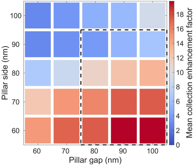
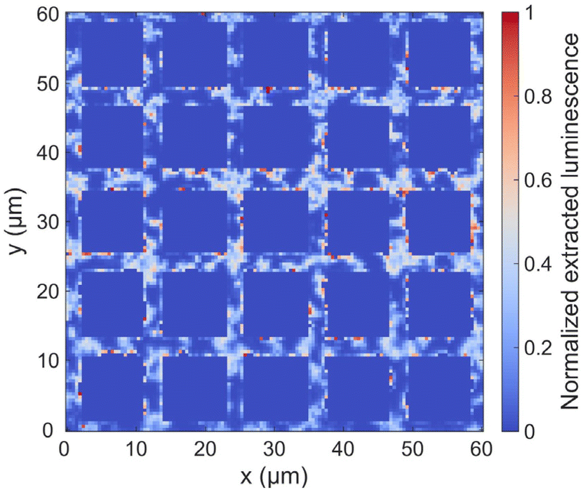
The CsPbBr3 layer consisting of QDs (see Materials and methods section for fabrication details) sits on a series of Mie resonators formed by square silicon nanopillars of lateral size L and separation g, which we denote by their geometrical parameters (L,g), as schematically depicted in Fig. 1. Each Mie resonator covers a 10 × 10 μm2 area (see Fig. 2a) and is separated from neighboring Mie resonators by a ∼3 μm distance (Fig. 1c and 2b). We studied 25 of these Mie resonators at room temperature using microphotoluminescence excited with a 405 nm laser. The wavelength-integrated spatially-resolved luminescence of the perovskite layer at approximately 532 nm is displayed in Fig. 1c, where we notice a strong enhancement of the luminescence signal from CsPbBr3 QDs located on Mie resonators. Indeed, the PL intensity averaged over the silicon areas with no pillars (regions shown in Fig. 2b in between two Mie resonators) is ∼18 times smaller than the maximum averaged extracted luminescence obtained on the (60 nm, 100 nm) resonator. Thus, by combining dielectric Mie resonators, which do not suffer ohmic losses of typical plasmonic resonators, one can enhance the luminescence of the perovskite layer almost twenty times compared to the same QDs layer deposited directly on silicon. | ||
| Fig. 1 (a) Schematic representation of the CsPbBr3 layer deposited on Mie resonators, each corresponding to a set of (L,g) parameters. (b) Geometric parameters defining the size of the square pillars (L) and their side-to-side separation, which we refer to as the gap (g). (c) Perovskite luminescence, normalized to the maximum intensity of the image, over Mie resonators with varying (L,g) parameters. | ||
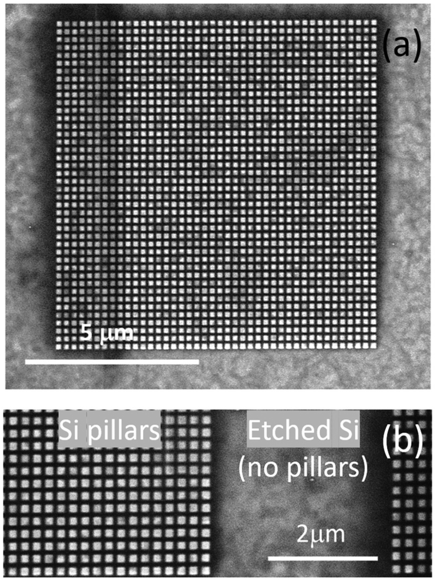 | ||
| Fig. 2 (a) Scanning electron microscopy image of a complete Mie resonator etched onto silicon, on a silicon-on-sapphire substrate, and covered by the perovskite QDs layer. (b) Scanning electron microscopy image at the border between two Mie resonators with different (L,g) parameters highlighting the quality of the pillars and the presence of a flat silicon surface (i.e. with no pillars) in between. | ||
To unravel the physical origin of this emission enhancement, we compared the experimental measurements with numerical calculations. However, one must note that there are strong intensity fluctuations within one Mie resonator (Fig. 1c). These intensity fluctuations occur on spatial scales much larger than the pillar separation and, thus, cannot be related to either an effect of the dielectric antennas on the distribution of QDs or to an effect of the inhomogeneous field distribution, whose variations are on much smaller spatial scales. They should rather be attributed to an inhomogeneous distribution of QDs within the layer associated with the synthesis or deposition process. To further confirm the origin of these intensity fluctuations we measured the PL distribution in the regions in between Mie resonators (region denoted by “Etched Si” in Fig. 2b); the PL signal from these regions, which do not contain any pillar (see Fig. 8 in the “Materials and methods” section), displays spatial inhomogeneities whose scale is exactly the same as on the Mie resonators. This observation confirms that the PL spatial fluctuations are not related to the resonators themselves, which are extremely homogenous (Fig. 2). To take these PL fluctuations into account and to be able to compare with numerical simulations, we will assume that they are independent of the surface onto which the CsPbBr3 QDs were deposited. As a result, we can average the luminescence across a Mie resonator and associate one overall intensity value to each (L,g) resonator as well as to the overall luminescence intensity from regions with no pillars.
Single-dipole picture: numerical simulations
Dielectric nanoantennas and associated resonators have been exploited in recent years due to their ability to interact with light through both electric (typically found in metallic nanoparticles) and magnetic resonances.20–23 In all these realizations, independent of the actual size and form of the dielectric antenna, the intensity field distribution is spatially inhomogeneous both inside and outside the dielectric antenna.To analyze the consequences of the field inhomogeneity for the emission properties of perovskite QDs, we first calculate the Purcell enhancement factor (Fig. 3a), which mimics the field distribution weighted by the corresponding polarization, for x-polarized dipoles radiating at 532 nm and distributed homogeneously around (i.e. both on top and in between the pillars) each silicon pillar constituting the Mie resonators (see Materials and methods section for more details on the numerical simulations and symmetry considerations). Under these conditions, the maximum Purcell enhancement factor is obtained for dipoles located along the x-axis between two consecutive pillars and relatively close to the pillars border: a maximum Purcell enhancement factor of about six is calculated. However, if CsPbBr3 QDs are homogeneously distributed over the entire resonator, most of them display actually a much smaller Purcell factor. This is one of the reasons why, in most experiments addressing Purcell enhancement in 3D resonators, the measured values are often far from optimal values,2,24 while they are much closer to them in planar cavities, where the in-plane position of the emitters does not matter.18,25 In fact, in some of early Purcell enhancement studies on epitaxial semiconductor QDs coupled to 3D cavities, it was already found that the measured Purcell factor is roughly given by the spatial average of the Purcell factor distribution.2
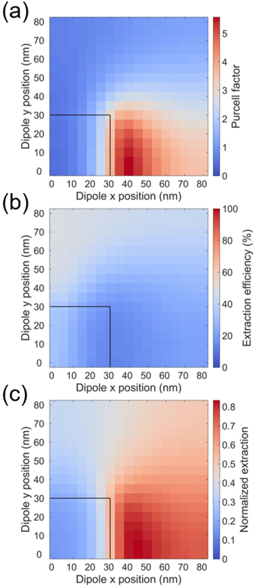 | ||
| Fig. 3 (a) Simulated Purcell factor as a function of dipole position. (b) Simulated extraction efficiency as a function of dipole position. (c) Simulated overall extracted intensity, normalized by dipole emission, as a function of dipole position within the Mie resonator. Note that this magnitude combines the effect of Purcell enhancement (or inhibition) and extraction due to the Mie resonator. The dipole is x-polarized and radiates at 532 nm. The (L,g) parameters for this structure are (60, 100). | ||
However, in emitting devices the Purcell effect is not the only factor determining the number of photons collected. High extraction efficiency is also necessary, which has been a bottleneck both in the field of single-photon quantum emitters26,27 and in conventional LEDs.28,29 To illustrate the importance of the extraction efficiency and highlight the asymmetry between the spatial distributions of the Purcell factor and of the extraction efficiency, we plot the local extraction efficiency in Fig. 3b for the same resonator as in Fig. 3a and for dipoles displaying the same polarization (parallel to the x-axis). One can first notice that while in Fig. 3a the maximum Purcell enhancement is achieved close to the resonator border, along the x-direction joining two neighboring pillars, in Fig. 3b the maximum extraction efficiency is obtained at locations farther apart from the resonator border (compared to the Purcell distribution) and, besides, the maximum is located along the y-direction joining two consecutive pillars i.e. at 90° with respect to the maximum Purcell enhancement. This asymmetry between the extraction efficiency and the Purcell enhancement can thus counterbalance the contribution of emitters with different Purcell factors and imposes, therefore, the knowledge of the two magnitudes to get a quantitative picture.
It is interesting to note, however, that since the local extraction efficiency changes by a factor ∼2 while the Purcell enhancement changes by a factor up to ∼6, the spatially-resolved response of the system (Fig. 3c) resembles more the spatial distribution of the Purcell enhancement than that of the local extraction efficiency.
Purcell enhancement: experiment and simulations
The ability of the Mie resonators to modify (accelerate or inhibit) the spontaneous emission rate of CsPbBr3 QDs is described by the Purcell factor. To estimate it we first measured the lifetime of perovskite QDs in four different regions with no pillars. This yielded a mean lifetime of about τoff-Mie = 5.9 ± 1.4 ns, which is comparable to the lifetime of CsPbBr3 nanocrystals synthesized by other methods in the litterature.19,30 Subsequently, and for reliability considerations, we measured the lifetime of perovskites QDs at four different locations within each Mie resonator.The average lifetimes for each (L,g) resonator are given in Fig. 4a, where a two/three-fold reduction of the lifetime is systematically observed with respect to the lifetimes measured in regions with no pillars. If we assume that these lifetimes, which span the 1.9 ± 0.2 ns to 3.6 ± 0.2 ns range, correspond to the radiative lifetimes of the CsPbBr3 QDs, then the Purcell enhancement factor can be easily obtained by calculating the ratio fPurcell = τon-Mie/τoff-Mie, which gives values between 3.1 and 1.6 for the Mie resonators.
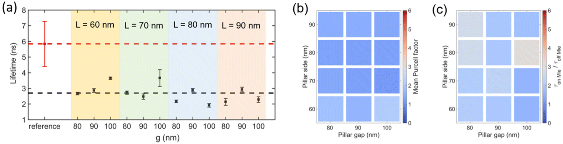 | ||
| Fig. 4 (a) Measured mean luminescence lifetime of CsPbBr3 QDs in regions with no pillars (red square) and on Mie resonators (black squares) characterized by (L,g) geometric parameters in the range L(60 nm–90 nm) and g(80 nm–100 nm), grouped by constant L. The selected (L,g) resonators correspond to those in the bottom right corner of Fig. 1, which are those indicated by a dashed line in Fig. 5. The error bars correspond to the root mean square deviations of the measured lifetimes in each region or resonator. (b) Simulated mean Purcell factor for Mie resonators characterized by (L,g) geometric parameters in the range L(60 nm–90 nm) and g(80 nm–100 nm). (c) Measured mean luminescence lifetime for Mie resonators characterized by (L,g) geometric parameters in the range L(60 nm–90 nm) and g(80 nm–100 nm), normalized by the lifetime of perovskites deposited on regions with no pillars. The scale for the averaged Purcell factors covers the values typically observed in the spatially-resolved calculations (Fig. 3(a)). | ||
While these Purcell values are substantially smaller than the maximum values we can expect for the studied Mie resonators (see for example Fig. 3a), they correlate fairly well with the computed Purcell factors when averaged over all possible spatial configurations within the resonators, as compared in Fig. 4b and c and observed in the late 1990s for epitaxial QDs coupled to pillar microcavities.2
Note that the Purcell factors extracted above rely on the assumption that these lifetimes correspond exclusively to the radiative recombination rate at each of the resonators. If one assumes a constant nonradiative recombination rate, i.e., insensitive to the presence or absence of the resonators, equal to the radiative recombination rate in the region with no pillars, the Purcell factors extracted from measured lifetimes would extend from ∼2 to ∼5, which would not significantly modify actual values (see ESI of ref. 25 for a detailed discussion of the effect of the nonradiative terms on the determination of the Purcell factor).
Overall extraction: experiment and simulations
From the spatially-resolved microphotoluminescence measurements in Fig. 1c we can assign an average photoluminescence value to each Mie resonator, leading to the intensity map in Fig. 5a. The effect of the Mie resonators geometrical parameters on the phenomena considered (Purcell enhancement and extraction) can be readily appreciated, with a fivefold relative variation among different Mie resonators. The comparison with the calculated values (Fig. 5(b)) obtained by spatially-averaging the individual dipole Purcell factors and extractions (i.e. taking into account Fig. 3 for each resonator) is excellent, both qualitatively and quantitatively, with an almost perfect match between both maps. | ||
| Fig. 5 (a) Spatially averaged luminescence intensity of CsPbBr3 QDs on Mie resonators with (L,g) geometric parameters in the range L(60 nm–90 nm) and g(60 nm–100 nm), normalized by the maximum average intensity corresponding to the (60 nm, 100 nm) resonator. (b) Simulated spatially-averaged extracted intensity, considering Purcell effect and extraction efficiency, on Mie resonators with (L,g) geometric parameters in the range L(60 nm–90 nm) and g(60 nm–100 nm), normalized by the maximum average intensity corresponding to the (60 nm, 100 nm) resonator. (c) Simulated spatially-averaged extracted intensity, considering Purcell effect, extraction efficiency and absorption at the excitation laser wavelength, on Mie resonators with (L,g) geometric parameters in the range L(60 nm–100 nm) and g(60 nm–100 nm), normalized by the maximum average intensity corresponding to the (70 nm, 100 nm) resonator. | ||
However, the Mie resonators we are working on display geometric (L,g) parameters that result in resonances in the visible wavelength region, as shown by the optical microscopy image of the resonators under white-light illumination (Fig. 6). These resonances can have a large impact on the reflectivity at the excitation laser wavelength (405 nm) and should therefore be taken into account to “numerically” reproduce actual photoluminescence experiments. For this purpose, we divide Fig. 5b by 1 − R − T, where R and T are the reflectivity and transmittance of Mie resonators at 405 nm. The result again agrees well qualitatively and quantitatively (Fig. 5c), although the maximum intensity is now obtained for a pillar side of 70 nm rather than a 60 nm pillar side.
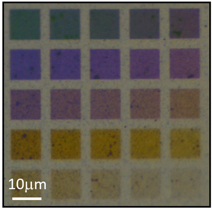 | ||
| Fig. 6 Bright-field optical microscopy image of Mie resonators characterized by (L,g) geometric parameters in the range L(60 nm–100 nm) and g(60 nm–100 nm). | ||
Discussion
The enhancement of perovskite luminescence by engineering one or several of the three processes discussed (i.e. pump absorption, Purcell effect and extraction efficiency) has already been accomplished by employing several types of resonators: metasurfaces,14 which provided 8-fold intensity enhancement with a moderate Purcell factor of about 2, hyperbolic metamaterials,30 which provided 4-fold intensity enhancement and can attain Purcell factors of up to 3.3,25 and metallic nanoresonators, which provided a spatially-localized 12-fold increase in luminescence intensity with a Purcell factor of about 3.Our approach employs a silicon platform, which is the most mature, cheap, compatible with large-scale production and arguably the simplest to process. Although the Mie resonators employed are fabricated by e-beam lithography, they are compatible with conventional nanoimprint machines in terms of feature size and result in an experimental 18-fold increase in photoluminescence intensity (Fig. 7). The fact that the spatially averaged Purcell factors are around 2–3 highlights the importance of the other two factors in achieving such a large photoluminescence enhancement. More importantly, our Mie resonators show an enhanced macroscopic response compared to metallic nanoresonators, which only enhance the photoluminescence intensity locally. Interestingly, our analysis shows that Mie resonators should provide a way to enhance emission rate as well as collection even in the case of single-emitters although, as with any single-photon source, this will require special care to place the single-emitter at a well-defined location within the inhomogeneous electric field distribution.
 | ||
| Fig. 7 Experimental intensity ratio between the spatially averaged luminescence intensity from Mie resonators and the mean luminescence intensity recorded in areas with no pillars. The Mie resonators are characterized by (L,g) geometric parameters in the range L(60 nm–100 nm) and g(60 nm–100 nm). | ||
Conclusions
A layer of CsPbBr3 QDs deposited on nanometric Mie resonators displays a two/three-fold reduction in average lifetime and, depending on the Mie resonator resonant wavelength, a photoluminescence enhancement of up to 18 times. A detailed numerical analysis that qualitatively and quantitatively reproduces the experimental results provides the necessary physical insight to decouple the individual contributions of pump absorption, internal quantum efficiency, and extraction efficiency to the overall enhancement. This excellent match opens the way to the design and development of realistically feasible dielectric nanoresonators capable of even greater luminescence enhancement.Materials and methods
Materials
Caesium carbonate (Cs2CO3, 99.9%), lead(II) bromide (PbBr2, >98%), oleylamine (technical grade 70%), 1-octadecene (90%), oleic acid (90%), cyclohexane (>98%), ethanol (>99%) were purchased from Sigma-Aldrich and used as-received without further treatment.Cs-oleate precursor synthesis
The Cs-oleate precursor synthesis followed the same procedure as described in the previously reported method.31 In a typical synthesis process, Cs2CO3 (0.4 g, 1.23 mmol), oleic acid (1.25 ml), and 1-octadecene (15 ml) were added to a two-necked round-bottomed flask (50 ml). The mixture was then heated to 100 °C for 0.5 h under vigorous stirring and vacuum conditions. Subsequently, the flask was alternately purged with nitrogen (N2) and placed under vacuum to remove moisture and O2. Then the mixture was heated to 150 °C until the solution became clear, indicating the completion of the reaction between Cs2CO3 and oleic acid. The as-obtained Cs-precursor solution was kept at 150 °C in N2 atmosphere before the synthesis of perovskite quantum dots.CsPbBr3 QD synthesis
The synthesis of CsPbBr3 QDs was carried out according to the previously reported method with minor modifications.31,32 In a typical experiment, PbBr2 (0.36 mmol), oleic acid (1.0 mL), oleylamine (1.0 mL), and octadecene (10 mL) were added to a two-necked round-bottomed flask (50 mL). The reaction mixture was heated to 100 °C with vigorous stirring and kept in vacuo for 30 min. Then the flask was purged with N2 and subsequently placed under vacuum. The moisture residue was removed by alternatively applying N2 and vacuum several times. After that, the reaction mixture was heated to 160 °C to completely dissolve the PbBr2 precursor. Then, a hot Cs-oleate precursor solution (1 mL) was quickly injected into the above-mentioned mixture. After 30 min of reaction, the flask was transferred to an ice bath. The CsPbBr3 QDs were obtained by centrifugation at 13![[thin space (1/6-em)]](https://www.rsc.org/images/entities/char_2009.gif) 000 rpm for 10 min and stored in 4 mL of cyclohexane for further use.
000 rpm for 10 min and stored in 4 mL of cyclohexane for further use.
Deposition of CsPbBr3 QDs on the Mie resonator
One milliliter QDs solution was pipetted into a 2 ml glass vial and then ultrasonicated for about 10 seconds. 1 drop of the solution was spin-coated onto the prepared Mie resonator sample at a speed of 2000 rpm for 60 s to form a homogeneous QDs layer. The above spin-coating procedure was repeated 5 times before completion of the CsPbBr3 QDs on Mie resonator sample.The CsPbBr3 QDs synthesis and/or deposition processes lead to a spatially-inhomogeneous distribution of emitters within the deposited layer, which can be assessed by monitoring the spatially-resolved PL intensity in the regions outside the Mie resonators (Fig. 2b). As shown in Fig. 8, PL intensity fluctuations with a typical spatial scale in the order of ∼μm are observed, similar to the PL intensity fluctuations on top of the Mie resonators (Fig. 1c). Note that the absolute emission intensity averaged over the silicon regions with no pillars (Fig. 8) is 18 times smaller than the averaged extracted luminescence from the (60 nm, 100 nm) Mie resonator in Fig. 1.
 | ||
| Fig. 8 Spatially-resolved perovskite luminescence normalized to the maximum intensity of the image on the silicon regions with no pillars, highlighted in Fig. 2b. Note that the PL signal from the perovskite-on-Mie resonators, which is roughly ten to twenty times more intense, has been removed in the current image. | ||
Mie resonator fabrication
Hydrogen silsesquioxane (HSQ) resist (Dow Corning XR-1541-002) was spin coated onto a cleaned 130 nm-thick silicon film on sapphire (Si Valley Microelectronics, Inc.), with a spin speed of 5000 round-per-minute (rpm) to obtain a resist thickness of ∼30 nm. Electron beam exposure was carried out on an Elionix ELS-7000, with an acceleration voltage of 100 keV, a beam current of 500 pA, and an exposure dose of ∼12 mC cm−2. The sample was then developed by a salty solution (NaOH/NaCl with the respective concentrations of 1 wt%/4 wt% in deionized water) for 60 seconds and then immersed in deionized water for another 60 seconds. After that, the sample was rinsed with acetone, isopropanol alcohol, and dried with an air gun. Si etching was carried out with inductively coupled plasma (ICP, Oxford Instruments Plasmalab System 100), with a DC power of 100 watts, a coil power of 500 watts, using a Cl2 flow rate of 22 sccm (standard cubic centimeters per minute), at a process pressure of 10 mTorr and a temperature of 6 °C.33 The residual Si layer after dry etching is around 20 nm.Numerical methods
FDTD simulations were conducted on a system made of a 20 nm thick perovskite layer on a 5 × 5 square-based silicon pillar matrix, which in turn is on a 20 nm thick silicon layer covering the whole sapphire substrate. The optical constants of silicon and sapphire were taken from ref. 34, while the perovskite refractive index (real and imaginary parts) were extracted from ref. 35.FDTD boundary conditions were set to PML, and the mesh size was set to 20 nm in all directions within the perovskite and silicon regions, while it was non-uniform out of these regions to reduce the calculation effort. An x-polarized dipole emitting at 532 nm is placed at the mid-height of the perovskite layer, and its (x,y) position is varied in a 11 × 11 square matrix, where x and y cover all values from the center of a pillar to the middle position towards two of its nearest neighboring pillars at 90° direction. The square symmetry of the lattice and the motif (i.e. the pillar) enable to simulate the whole unit cell of the pillar matrix with the previous calculation, and from that extend to the whole matrix. Note that due to the previously indicated square symmetry, in-plane x- and y-polarized dipoles are equivalent. On the other hand z-polarized dipoles emit radiation mostly parallel to the structure and the numerical simulations indicate a negligible contribution to the extracted luminescence normal to the Mie resonator.36
Finally, it should be noted that while all the numerical simulations shown in the paper considered a 20 nm-thick perovskite layer, the actual enhancement factors only vary in the order of 20% when considering perovskites thicknesses smaller than 50 nm. Beyond this thickness, i.e. beyond roughly λ/4n ∼ 66 nm (λ being the perovskite emission wavelength and n being the perovskite refractive index), interference effects need to be considered and the position of the emitters along the z direction becomes important. As indicated in the Introduction section, this dependence has been treated in earlier works for planar resonators and is not the main focus of the current paper.
Author contributions
R. H. performed the optical measurement and characterization. M. M. and J. Z. P. performed the numerical simulations and data analysis. Z. D. fabricated the silicon nanoantennas with Mie resonances. H. C. prepared the sample. X. L. and W. G. conceived the experiment and managed the research. J. Z. P. wrote the manuscript with inputs from all authors.Conflicts of interest
There are no conflicts to declare.Acknowledgements
This project has received financial support from the CNRS through the 80|Prime program. J. Z. P. would like to acknowledge funding support from CNRS Tremplin@INP2020. Z. D. would like to acknowledge the funding support from A*STAR AME IRG grant (Project No. A20E5c0093), A*STAR CDA grant (Project No. C210112019) and A*STAR MTC IRG grant (Project No. M21K2c0116). W. G. and X. L. acknowledges the funding support from National Research foundation through NRF-CRP23-2019-0002. J. Z. P. would like to acknowledge enlightening discussions with B. Gayral on the Purcell effect.References
- E. M. Purcell, Phys. Rev., 1946, 69, 681 CrossRef.
- J. M. Gérard, B. Sermage, B. Gayral, B. Legrand, E. Costard and V. Thierry-Mieg, Phys. Rev. Lett., 1998, 81, 1110 CrossRef.
- L. Protesescu, S. Yakunin, M. I. Bodnarchuk, F. Krieg, R. Caputo, C. H. Hendon, R. X. Yang, A. Walsh and M. V. Kovalenko, Nano Lett., 2015, 15, 3692 CrossRef CAS PubMed.
- F. Zhang, H. Zhong, C. Chen, X. G. Wu, X. Hu, H. Huang, J. Han, B. Zou and Y. Dong, ACS Nano, 2015, 9, 4533 CrossRef CAS PubMed.
- M. Yuan, L. N. Quan, R. Comin, G. Walters, R. Sabatini, O. Voznyy, S. Hoogland, Y. Zhao, E. M. Beauregard, P. Kanjanaboos, Z. Lu, D. H. Kim and E. H. Sargent, Nat. Nanotechnol., 2016, 11, 872 CrossRef CAS PubMed.
- G. Xing, B. Wu, X. Wu, M. Li, B. Du, Q. Wei, J. Guo, E. K. L. Yeow, T. Sum and W. Huang, Nat. Commun., 2017, 8, 14558 CrossRef CAS PubMed.
- H. Utzat, W. Sun, A. K. Kaplan, F. Krieg, M. Ginterseder, B. Spokoyny, N. D. Klein, K. E. Shulenberge, C. Perkinson, M. V. Kovalenko and M. G. Bawendi, Science, 2019, 363, 1068 CrossRef CAS PubMed.
- S. Castelletto, F. De Angelis and A. Boretti, Appl. Mater. Today, 2022, 26, 101401 CrossRef.
- Y. Jia, R. A. Kerner, A. J. Grede, A. N. Brigeman, B. P. Rand and N. C. Giebink, Nano Lett., 2016, 16, 4624–4629 CrossRef CAS PubMed.
- Z. Li, J. Moon, A. Gharajeh, R. Haroldson, R. Hawkins, W. Hu, A. Zakhidov and Q. Gu, ACS Nano, 2018, 12, 10968–10976 CrossRef CAS PubMed.
- N. Pourdavoud, T. Haeger, A. Mayer, P. J. Cegielski, A. L. Giesecke, R. Heiderhoff, S. Olthof, S. Zaefferer, I. Shutsko, A. Henkel, D. Becker-Koch, M. Stein, M. Cehovski, O. Charfi, H. H. Johannes, D. Rogalla, M. C. Lemme, M. Koch, Y. Vaynzof, K. Meerholz, W. Kowalsky, H. C. Scheer, P. Görn and T. Riedl, Adv. Mater., 2019, 31, 1903717 CrossRef PubMed.
- H. Kim, K. Roh, J. P. Murphy, L. Zhao, W. B. Gunnarson, E. Longhi, S. Barlow, S. R. Marder, B. P. Rand and N. C. Giebink, Adv. Opt. Mater., 2020, 8, 1901297 CrossRef CAS.
- B. Gholipour, G. Adamo, D. Cortecchia, H. N. S. Krishnamoorthy, M. D. Birowosuto, N. I. Zheludev and C. Soci, Adv. Mater., 2017, 29, 1604268 CrossRef PubMed.
- S. V. Makarov, V. Milichko, E. V. Ushakova, M. Omelyanovich, A. C. Pasran, R. Haroldson, B. Balachandran, H. Wang, W. hu, Y. S. Kivshar and A. A. Zakhidov, ACS Photonics, 2017, 4, 728–735 CrossRef CAS.
- Y. Fan, P. Tonkaev, Y. Wang, Q. Song, J. Han, S. V. Makarov, Y. Kivshar and S. Xiao, Nano Lett., 2021, 21, 7191 CrossRef CAS PubMed.
- H. Zhang, Q. Liao, Y. Wu, Z. Zhang, Q. Gao, P. Liu, L. Li, J. Yao and H. Fu, Adv. Mater., 2018, 30, 1706186 CrossRef PubMed.
- P. J. Cegielski, A. L. Giesecke, S. Neutzner, C. Porschatis, M. Gandini, D. Schall, C. A. R. Perini, J. Bolten, S. Suckow, S. Kataria, B. Chmielak, T. Wahlbrink, A. Petrozza and M. C. Lemme, Nano Lett., 2018, 18, 6915–6923 CrossRef CAS PubMed.
- J. Wang, R. Cao, P. Da, Y. Wang, T. Hu, L. Wu, J. Lu, W. Shen, F. Xu, G. Zheng and Z. Chen, Appl. Phys. Lett., 2016, 108, 022103 CrossRef.
- M. Athanasiou, P. Papagiorgis, A. Manoli, C. Bernasconi, M. I. Bodnarchuk, M. V. Kovalenko and G. Itskos, ACS Photonics, 2021, 8, 2120–2129 CrossRef CAS.
- A. I. Kuznetsov, A. E. Miroshnichenko, Y. H. Fu, J. Zhang and B. Luk'yanchuk, Sci. Rep., 2012, 2, 492 CrossRef PubMed.
- A. B. Evlyukhin, S. M. Novikov, U. Zywietz, R. L. Eriksen, C. Reinhardt, S. I. Bozhevolnyi and B. N. Chichkov, Nano Lett., 2012, 12, 3749–3755 CrossRef CAS PubMed.
- M. Decker, I. Staude, M. Falkner, J. Dominguez, D. N. Neshev, I. Brener, T. Pertsch and Y. S. Kivshar, Adv. Opt. Mater., 2015, 3, 813 CrossRef CAS.
- Z. Dong, J. Ho, Y. F. Yu, Y. H. Fu, R. Paniagua-Dominguez, S. Wang, A. I. Kuznetsov and J. K. W. Yang, Nano Lett., 2017, 17, 7620–7628 CrossRef CAS PubMed.
- G. Adamo, H. Natarajan, S. Krishnamoorthy, D. Cortecchia, B. Chaudhary, V. Nalla, N. I. Zheludev and C. Soci, Nano Lett., 2020, 20, 7906–7911 CrossRef CAS PubMed.
- H. P. Adl, S. Gorji, M. K. Habil, I. Suarez, V. S. Chirvony, A. F. Gualdron-Reyes, I. Mora-Sero, L. M. Valencia, M. de la Mata, J. Hernandez-Saz, S. I. Molina, C. J. Zapata-Rodriguez and J. P. Martinez-Pastor, ACS Photonics, 2020, 7, 3152–3160 CrossRef CAS PubMed.
- N. Somaschi, V. Giesz, L. De Santis, J. C. Loredo, M. P. Almeida, G. Hornecker, S. L. Portalupi, T. Grange, C. Anton, J. Demory, C. Gomez, I. Sagnes, N. D. Lanzillotti-Kimura, A. Lemaitre, A. Auffeves, A. G. White, L. Lanco and P. Senellart, Nat. Photonics, 2016, 10, 340–345 CrossRef CAS.
- X. Ding, Y. He, Z. C. Duan, N. Gregersen, M. C. Chen, S. Unsleber, S. Maier, C. Schneider, M. Kamp, S. Hofling, C. Y. Lu and J. W. Pan, Phys. Rev. Lett., 2016, 116, 020401 CrossRef PubMed.
- I. Schnitzer, E. Yablonovitch, C. Caneau, T. J. Gmitter and A. Scherer, Appl. Phys. Lett., 1993, 63, 2174–2176 CrossRef CAS.
- A. David, C. A. Hurni, R. I. Aldaz, M. J. Cich, B. Ellis, K. Huang, F. M. Steranka and M. R. Krames, Appl. Phys. Lett., 2014, 105, 231111 CrossRef.
- V. Caligiuri, M. Palei, M. Imran, L. Manna and R. Krahne, ACS Photonics, 2018, 5, 2287–2294 CrossRef CAS PubMed.
- Q. Chen, J. Wu, X. Ou, B. Huang, J. Almutlaq, A. A. Zhumekenov, X. Guan, S. Han, L. Liang, Z. Yi, J. Li, X. Xie, Y. Wang, Y. Li, D. Fan, D. B. L. Teh, A. H. All, O. F. Mohammed, O. M. Bakr, T. Wu, M. Bettinelli, H. Yang, W. Huang and X. Liu, Nature, 2018, 561, 88–93 CrossRef CAS PubMed.
- A. Swarnkar, A. R. Marshal, E. M. Sanehira, B. D. Chernomordik, D. T. Moore, J. A. Christians, T. Chakrabarti and J. M. Luther, Science, 2016, 354, 92 CrossRef CAS PubMed.
- Z. Dong, S. Goelik, R. Paniagua-Dominguez, J. Yik, J. Ho, F. Tjiptoharsono, E. Lassalle, S. D. Rezaei, D. C. J. Neo, P. Bai, A. I. Kuznetsov and J. K. W. Yang, Nano Lett., 2021, 21, 4853–4860 CrossRef CAS PubMed.
- E. D. Palik, Handbook of optical constants of solids, Academic Press, 1998, vol. 3 Search PubMed.
- M. Zhao, Y. Shi, J. Dai and J. Lan, J. Mater. Chem. C, 2018, 6, 10450–10455 RSC.
- L. Lin, R. P. Zaccaria, D. Garoli and R. Krahne, Nanomaterials, 2021, 11, 2947 CrossRef CAS PubMed.
| This journal is © The Royal Society of Chemistry 2023 |