
 Open Access Article
 This Open Access Article is licensed under a
 Creative Commons Attribution 3.0 Unported Licence
A DFT exploration of the optoelectronic and thermoelectric features of a novel halide double perovskite A2YAuI6 (A = Rb, Cs) for solar cell and renewable energy applications
Abrar
Nazir
a,
Aparna
Dixit
b,
Ejaz Ahmad
Khera
 *a,
Mumtaz
Manzoor
c,
Ramesh
Sharma
d and
A. J. A.
Moayad
*e
*a,
Mumtaz
Manzoor
c,
Ramesh
Sharma
d and
A. J. A.
Moayad
*e
aDepartment of Physics Bahawalnagar Campus, The Islamia University of Bahawalpur, Bahawalpur, 63100, Pakistan. E-mail: ejaz.khera@iub.edu.pk
bDepartment of Basic Sciences and Humanities, Pranveer Singh Institute of Technology, Kanpur, U. P, India
cInstitute of Physics, Slovak Academy of Sciences, 84511 Bratislava, Slovakia
dDepartment of Applied Science, Feroze Gandhi Institute of Engineering and Technology, Raebareli-229001, Uttar Pradesh, India. E-mail: sharmadft@gmail.com
eDepartment of Materials Science, Malawi University of Science and Technology, P. O Box 5196, Limbe, Malawi. E-mail: mailme_moya123@rediffmail.com
First published on 10th April 2024
Abstract
Double-perovskite halides are potentially useful materials for producing renewable energy and are thought to meet the necessary criteria for addressing energy scarcity issues. Consequently, investigations into these halides have potential uses in the fields of thermoelectric and solar cell gadgets. The physical properties of A2YAuI6 (A = Rb, Cs) double perovskite halides were also investigated in the current work using DFT calculations based on the FP-LAPW approach for applications in renewable energy devices. The calculated Goldschmidt's tolerance factor and formation energy demonstrate that the explored halides are structurally and thermodynamically stable in the cubic phase. By analyzing mechanical properties, the measured Pugh and Poisson ratios demonstrate a ductile nature. In addition, we used electrical characteristics to compute bandgaps both with and without spin orbit coupling (SOC). We calculated the bandgap values of Rb2YAuI6 (Eg = 1.73 eV) and Cs2YAuI6 (Eg = 1.70 eV) using modified Becke–Johnson with spin orbit coupling (mBJ + SOC) potentials in order to get corrected bandgap values with respect to experimental data. Additionally, the optical characteristics of the halides under study were analyzed in light of their complex dielectric functions. Our computed optical parameter results clearly show that these halides have the best light absorption in the UV-visible region, indicating their suitability for use in solar cell applications. The power factor (PF), thermal conductivity, figure of merit, electrical conductivity, and Seebeck coefficient were computed to analyze transport characteristics against chemical potential, carrier concentration and temperature. Our findings can prove beneficial for further experimental research aimed at assessing A2YAuI6 (A = Rb, Cs) in relation to applications using renewable energy devices.
1. Introduction
The demand for alternatives to fossil fuels has dramatically increased as a result of the shortage of traditional energy sources. The techniques that researchers are developing can draw energy from renewable resources. One of the primary sources of energy from renewable sources is the sun. Researchers can turn the heat and light energy from the sun into electrical energy using solar cells and thermoelectric generators. However, recent studies have shown that lead-involved hybrid perovskites can be created by mixing organic and inorganic components. Amongst the different material types, perovskites are one of the most popular materials that have been extensively explored for thermoelectric and photovoltaic applications, particularly in the field of perovskite solar cells. Perovskites are well-known for their cost-effectiveness, high absorption coefficient, adjustable bandgap, low effective mass, free availability, and stability in their structure. Moreover, they are simple to synthesize and low in weight.1–10 However, because of their low stability and toxicity, as seen in CH3NH3PbX3 (where X = Cl, Br and I) perovskites, they are hazardous to the environment and are of little utility in the solar cell system.1–3 Lead-free material manufacturing is therefore urgently needed. Using lead-free products can help to protect the environment as well as reduce the need for fossil fuels. Consequently, lead-free double perovskites have drawn much interest from the scientific community.Among the subclasses of perovskite structure, double perovskites has properties that combine the chemical and physical characteristics, whereas we cannot see these properties in a simple perovskite structure. These materials come in a greater variety of metals and oxidation states. This diversity makes it possible to enhance the optoelectronic characteristics that are beneficial for solar energy technologies. Shi et al.11 created lead-free double perovskites that relax ferroelectrics in order to investigate the piezoelectric behavior. These rare-earth perovskites have great qualities that make them appropriate for solar energy applications. Still, a large number of researchers substituted tin-based halide perovskites for lead-based perovskites, specifically CH3NH3PbX3.12–14 Researchers are searching for various perovskites that could be used as solar absorber materials because of the breakdown and instability of these perovskites.15–17 Lead-free double perovskite Cs2AgBiX6 has been the subject of recent investigations, and considered as an environmentally friendly substitute for CH3NH3PbI3.18 Wang et al. have proposed the use of double perovskite Cs2AgBiBr6 in conjunction with reduced graphene oxide to produce photocatalytic hydrogen.19 The optical, thermoelectric, magnetic and electronic characteristics of the Ca2Cr1−xNixOsO6 double perovskites were observed by Bhandari et al.20 using density functional theory. The results demonstrated that the double perovskite that was produced had a bandgap of around (0.6 eV), and was optically isotropic and ferromagnetic. The fact that compounds with narrow bandgaps, such as PbTe and Bi2Te3,21 are thought to be appropriate for thermoelectric generators is highly interesting. According to a study carried out by Haque et al.,22 Cs2InAgCl6 has a direct band gap of 3.3 eV with a ZT value of 0.94 that makes it appropriate for thermoelectric appliances.
The optoelectronic and thermoelectric features of Cs2ScAgY6 (Y = Cl, Br and I) have been studied by Khan et al.23 These compounds have demonstrated indirect bandgap values of 1.55 eV and 1.9 eV at 300 K, as well as a figure of merit value of 0.74. X2ScInI6 (X = Rb, Cs) was examined using DFT by Noor et al.,24 and they were shown to be useful for optoelectronic devices. Iqbal et al. previously studied the opto-electronic and transport characteristics of Rb2AlInX6 (X = Cl, Br, I).25 By applying first-principle computations, Anbarasan et al.26 reported the mechanical, structural, and opto-electronic features of Cs2AgInY6 (Y = Cl, Br and I). Nazir et al.27 has examined the double perovskite X2LiInBr6 (X = Rb, Cs) for solar cell applications. Due to their absorption and optical conductivity in the visible region of the electromagnetic spectrum, they are suitable candidates for solar cell applications.
In the present study, we have computed the structural, electronic, optical, and thermoelectric properties of novel double perovskite A2YAuI6 (A = Rb, Cs) compounds. As per our knowledge, neither experimental nor theoretical study has been performed earlier for these compounds. Our results would hopefully be helpful for future experimental and theoretical research studies in evaluating the A2YAuI6 (A = Rb, Cs) double perovskite for applications related to energy harvesting technologies.
2. Methodology
In our study, we used FP-LAPW28,29 method-based WIEN2k code28 to compute the optoelectronic and transport characteristics of Rb2YAuI6 and Cs2YAuI6via DFT calculations. Using Murnaghan equations of states for the examined compounds, the PBE-GGA functional was utilized to precisely calculate the lattice constants, ground state energy, and bulk modulus.30–32 Although it facilitates the computation of structural parameters, this approximation underestimates electronic parameters, particularly the band gap. Despite having comparable accuracy, the TB-mBJ33 potential is more flexible and requires less computation time than the PBE-GGA.34 Therefore, the TB-mBJ potential is applied over PBE-GGA in order to accurately measure the band gap. Additionally, since the SOC coupling influences the band gap materials of heavy elements, it has also been included. While the electronic system solution is plane wave-like in the interstitial area, it is believed to be spherically harmonic within the muffin-tin sphere. The structure is continuously optimized until the strain-force for every atom is zero. The starting parameters have been adjusted by setting the angular momentum![[small script l]](https://www.rsc.org/images/entities/i_char_e146.gif) max = 10 in the reciprocal lattice, Gaussian parameter Gmax = 14, and the product of the wave vector and muffin radius Kmax × RMT = 8. When the energy released from the system becomes constant, the 2000 k-point is used to select the k-mesh of the order of 12 × 12 × 12.35 The optical properties were calculated by employing Kramers–Kronig equations. This is thought to be the convergence criterion's threshold limit in terms of the precision of the results acquired. The charge convergence is taken into account at 0.01 mRy. For the separation of the core and valence states, the cut-off energy was selected as −9 Ry. The core state is explained by the lower energy range compared to those equipped states. The thermoelectric parameters, such as the Seebeck coefficient, electrical conductivity, thermal conductivity, figure of merit (ZT) and power factor, were calculated in the temperature range of 100–1200 K against chemical potential and carrier concentration. The Boltztrap code,36 which is based on the classical Boltzmann transport theory, was used to calculate the transport features by utilizing the optimized electrical structures via Tb-mBJ and the convergent energy. For the thermoelectric characteristics calculation, a fine grid mesh has been utilized (44 × 44 × 44).
max = 10 in the reciprocal lattice, Gaussian parameter Gmax = 14, and the product of the wave vector and muffin radius Kmax × RMT = 8. When the energy released from the system becomes constant, the 2000 k-point is used to select the k-mesh of the order of 12 × 12 × 12.35 The optical properties were calculated by employing Kramers–Kronig equations. This is thought to be the convergence criterion's threshold limit in terms of the precision of the results acquired. The charge convergence is taken into account at 0.01 mRy. For the separation of the core and valence states, the cut-off energy was selected as −9 Ry. The core state is explained by the lower energy range compared to those equipped states. The thermoelectric parameters, such as the Seebeck coefficient, electrical conductivity, thermal conductivity, figure of merit (ZT) and power factor, were calculated in the temperature range of 100–1200 K against chemical potential and carrier concentration. The Boltztrap code,36 which is based on the classical Boltzmann transport theory, was used to calculate the transport features by utilizing the optimized electrical structures via Tb-mBJ and the convergent energy. For the thermoelectric characteristics calculation, a fine grid mesh has been utilized (44 × 44 × 44).
3. Structural and mechanical properties
For all computations, we used the crystal structures of the Rb2YAuI6 and Cs2YAuI6 compounds with the space group of Fm![[3 with combining macron]](https://www.rsc.org/images/entities/char_0033_0304.gif) m #225. The crystal structure of A2YAuI6 (A = Rb, Cs) is presented in Fig. 1. Using the Murnaghan equation37 of states, we optimized both compounds using PBE-GGA to obtain the ground state lattice parameters.
m #225. The crystal structure of A2YAuI6 (A = Rb, Cs) is presented in Fig. 1. Using the Murnaghan equation37 of states, we optimized both compounds using PBE-GGA to obtain the ground state lattice parameters. | (1) |
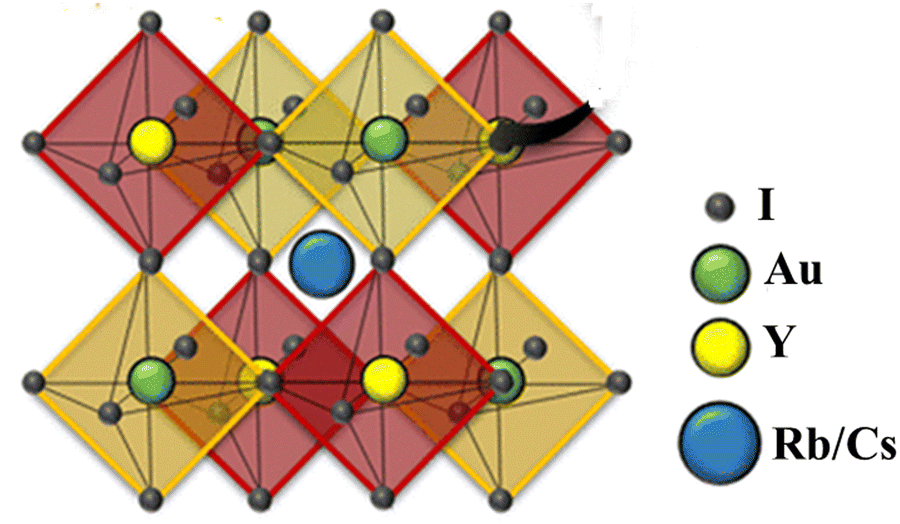 | ||
| Fig. 1 Crystal structure of A2YAuI6 (A = Rb, Cs). | ||
The bulk modulus and ground state lattice constant (a0) are determined via the volume optimization method, as depicted in Table 1. The ground state energy versus optimized volume graphs of studied compounds are shown in Fig. 2. The determined values of a0 increase from Rb2YAuI6 to Cs2YAuI6, as shown in Table 1, because the atomic radii increase from 2.48 Å (Rb) to 2.65 Å (Cs). The increase in cationic size leads to a decrease in the density (and therefore the solidity of the materials), which is why the bulk modulus B0 (20.33 GPa 19.87 GPa) drops when Rb replaces Cs. Applying the formula,38 we determine Goldschmidt's tolerance factor (tG) for the computation of structural stability.
 | (2) |
| ΔHf = ETotal (Rb/CsaYbAucId) − aERb/Cs − bEY − cEAu − dEI | (3) |
![[thin space (1/6-em)]](https://www.rsc.org/images/entities/char_2009.gif) 222.705247
222.705247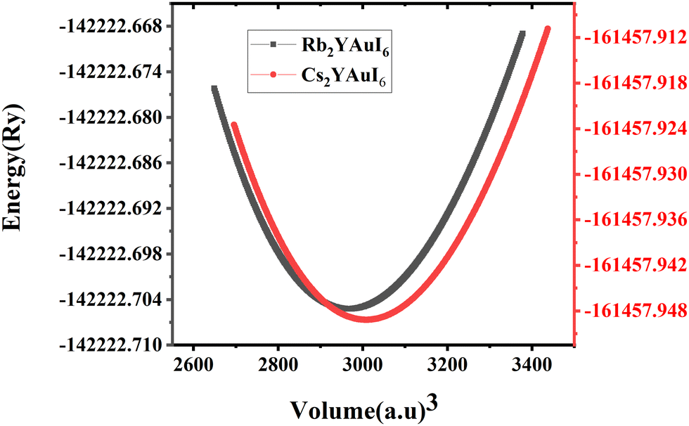 | ||
| Fig. 2 Energy versus volume optimization curves of A2YAuI6 (A = Rb, Cs). | ||
| Material property | Rb2YAuI6 | Cs2YAuI6 | Rb2ScInI624 | Cs2ScInI624 | Rb2LiGaI627 | Cs2LiGaI627 |
|---|---|---|---|---|---|---|
| Bulk modulus, B (GPa) | 20.33 | 19.87 | 19.42 | 18.93 | 14.3699 | 18.6031 |
| Shear modulus, G (GPa) | 1.41 | 1.16 | 6.55 | 3.64 | ||
| t G | 0.954 | 0.995 | 0.95 | 0.97 | 0.9021 | 0.8152 |
| Formation energy ΔHf | −1.296 | −1.335 | −1.04 | −1.16 | ||
| Young modulus, E (GPa) | 4.15 | 3.43 | 17.67 | 10.24 | 18.8063 | 25.3824 |
| Poisson ratio, σ (GPa) | 0.47 | 0.47 | 0.245 | 0.232 | ||
| Pugh ratio, B/G (GPa) | 2.01 | 1.86 | 2.96 | 5.2 | 1.626 | 1.532 |
| Cauchy pressure CP (GPa) | 18 | 17.9 | ||||
| Transverse sound velocity (m s−1) | 2092 | 1774 | ||||
| Longitudinal sound velocity (m s−1) | 3203 | 2874 | ||||
| Average sound velocity (m s−1) | 2293 | 1956 | ||||
| Temperature ΘD (K) | 193.4 | 164.3 | 197.72 | 148.81 |
The compounds are classified as ductile (B/G > 1.75) and brittle (B/G < 1.75) based on the critical limit of 1.75 of Pugh's ratio (B/G). The ductile criterion for the materials is defined by the Poisson ratio (υ), which is defined as σ greater than 0.26.40 It has been demonstrated that Cs2YAuI6 is more ductile than Rb2YAuI6 due to its greater B/G and υ values. Using the Navier equation of states, we can also compute the sound velocity as the mean of the transverse and longitudinal components of the velocities.41,42 However, Rb2YAuI6 has a greater value than Cs2YAuI6. This directly affects the Debye temperature, which is determined using the following formula:
 | (4) |
4. Electronic properties
One of the most crucial electronic properties that aids in understanding a compound's device applications is its band gap, which offers a thorough explanation of its optical, electronic, and thermodynamic characteristics. We calculated the band structures of Rb2YAuI6 and Cs2YAuI6 by using PBE-GGA, TB-mBJ potential with and without spin orbit coupling (SOC) in order to analyze the electronic structure properties, as depicted in Fig. 3(a–f). The numerical values of the electronic band structure are presented in Table 3. Furthermore, as shown in Fig. 3(a–d), we identified substantially underestimated energy band gap values for the examined compounds utilizing the PBE-GGA technique. Based on this, the Tb-mBJ functional is a better exchange correlation functional for improving the optoelectronic features.44 The energy band gap of 1.77 eV and 1.72 eV has been observed for Rb2YAuI6 and Cs2YAuI6, respectively, by the Tb-mBJ potential. Applying SOC is essential in order to acquire the right bandgap values in relation to the values derived from experiments.45 Consequently, we employed mBJ + SOC potentials to explore the Cs2YAuI6 (Eg = 1.73 eV) and Rb2YAuI6 (Eg = 1.70 eV) bandgap values. The band gap decreased as the atomic numbers of A (Rb, Cs) increased. The well-known inter-site exchange interactions can be connected to this. This has a direct relationship with the coinciding orbital overlaps, which scale inversely with the lattice constants.46 Furthermore, the bands have been divided by the spin–orbit coupling (SOC). It was found that the SOC splitting inside the valence/conduction bands was stronger, and decreased the band gap width with bigger elemental components.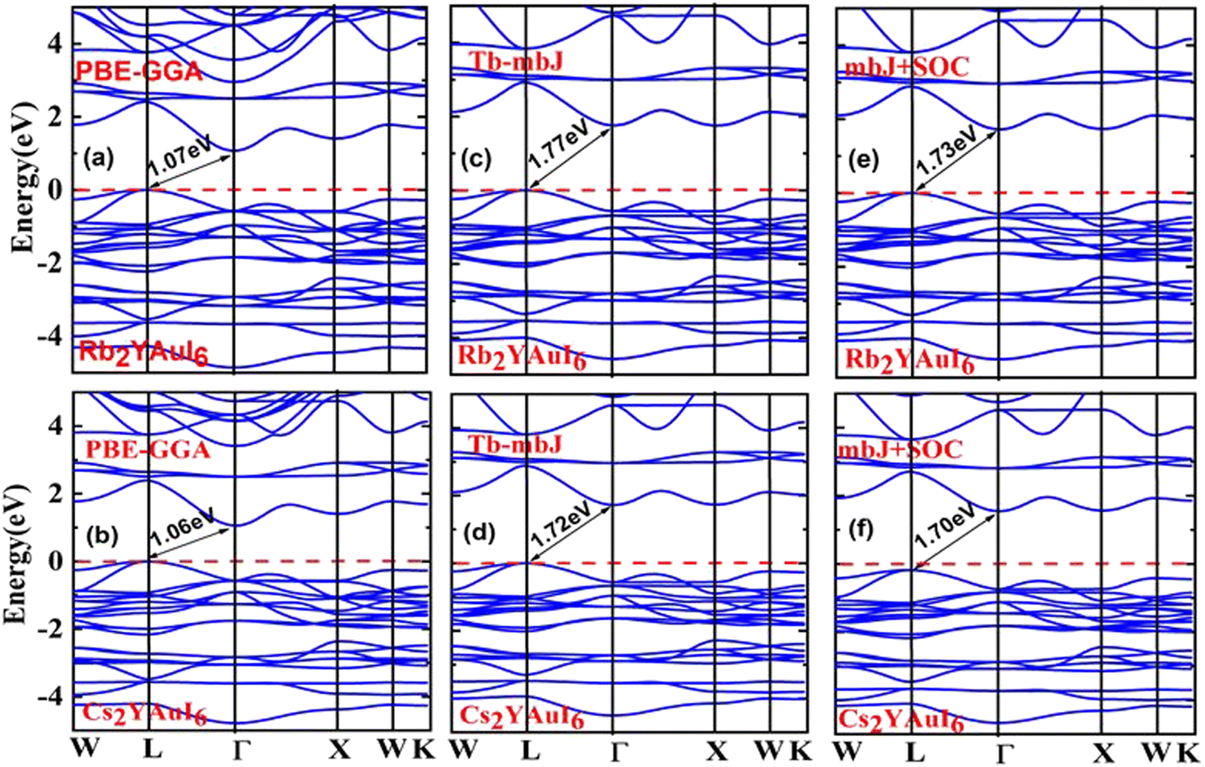 | ||
| Fig. 3 Representations of the band structures of A2YAuI6 (A = Rb, Cs) using (a, b) PBE-GGA, (c, d) TB-mBJ and (e, f) mBJ + SOC approximation. | ||
| Properties | PBE | mBJ | mBJ + SOC |
|---|---|---|---|
| Rb2YAuI6 | 1.07 | 1.77 | 1.73 |
| Cs2YAuI6 | 1.06 | 1.72 | 1.70 |
Total Density of States (TDOS) has been computed for the purpose of verifying the results of the energy band structure study. The Fermi level is shown by a vertical dashed line in all partial density of states (PDOS) and total density of states (TDOS) graphs. The energy plots range from −10 eV to 10 eV. Conduction band (CB) states appear at positive energy, whereas the valence band (VB) states are present at negative energy. The total of the individual states is shown by TDOS in both conduction and valence bands resembling the band structure. The total density of states TDOS results are depicted in Fig. 4(a and b).
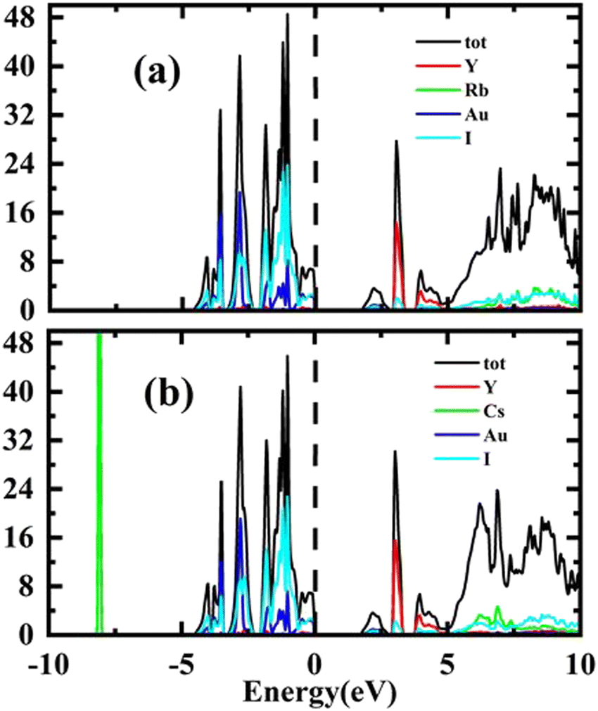 | ||
| Fig. 4 Representations of the TDOS of (a) Rb2YAuI6, (b) Cs2YAuI6 using Tb-mBJ approximation. | ||
The results of PDOS for the studied compounds that describe the orbital contribution to the electron conduction mechanism are elaborated in Fig. 5(a and b). For Rb2YAuI6, the valence band formation is due to hybridization of the Au-5d and I-5p states. Meanwhile, the conduction band is occupied due to the hybridization of the Y-4d and Rb-5p states with a negligible contribution of the Au-5p states. In the case of Cs2YAuI6, the valence band is formed due to hybridization of electrons from I-5p and Au-5p and a nominal contribution of Cs-6s. However, the conduction band is occupied by hybridization of the Y-4d and Cs-4d states and a negligible contribution of the I-5p and Au-5p states.
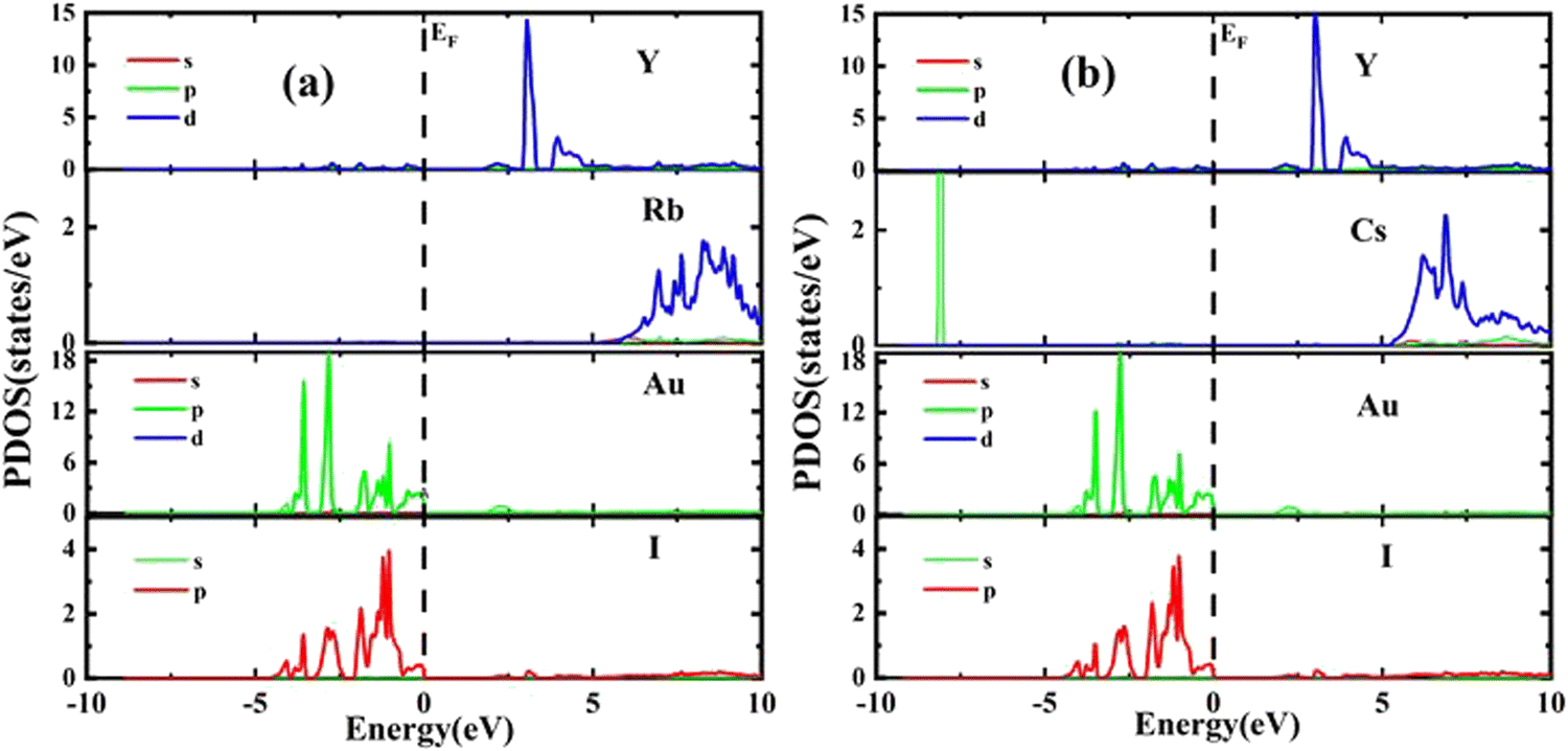 | ||
| Fig. 5 Representations of the PDOS of (a) Rb2YAuI6, (b) Cs2YAuI6 using Tb-mBJ approximation. | ||
4.1 The ELF and bader charge analysis
To investigate the nature of the bond identified between the constituents of the examined material, the electron localization function (ELF) is determined,47 as illustrated in Fig. 6(a and b). The ELF is based on the probability density of locating an electron at a certain position in space, and offers information about how localized or delocalized the electrons are. There is no charge between the components of an ionic connection, in contrast to atoms in covalent and metallic bonds sharing a charge. Fig. 6 shows the spatial charge configuration for the Rb2YAuI6 and Cs2YAuI6 perovskites.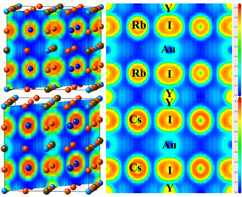 | ||
| Fig. 6 Representations of the ELF of A2YAuI6 (A = Rb, Cs) along the 101 plane direction using PBE-GGA approximation. | ||
There are no charge contours that cross over to overlap with the I atoms in the perfectly spherical charge distribution between Rb and Y/Au. It was shown that there was an ionic connection between the I atom and the Cs, Rb atoms. In contrast, the Rb charge distribution varies from perfectly spherical to distorted, leading to a covalent interaction with the Cs atom (dumbbell type). It has been established that I accepts electrons from the Au network due to its covalent characteristics.
5. Optical properties
The optical properties were thoroughly explored in order to identify the importance of the computed material for solar cell applications. The optical performance of the transition study from the valence to the conduction band was examined. The optical properties are illustrated by the relative positions of light and materials. The intensity of light emission and absorption for optoelectronic devices is determined by the inter- and intra-band transitions.The complex dielectric function (ε(ω)), absorption coefficient (α(ω)), complex refractive index (n(ω)), reflectivity R(ω), loss function L(ω) and optical conductivity σ(ω) have all been examined in relation to the optoelectronic features. The complex dielectric (CD) functions48 are represented as follows:
| ε(ω) = ε1(ω) + iε2(ω) | (5) |
Fig. 7(a and b) displays the energy value 0–12 eV of the CD function plot. The dielectric constant has two parts: the imaginary part is denoted by ε2(ω), and the real part represents ε1(ω). The real and imaginary components of the dielectric function are related by the most familiar Kramers–Kronig equations,49 which are given as:
 | (6) |
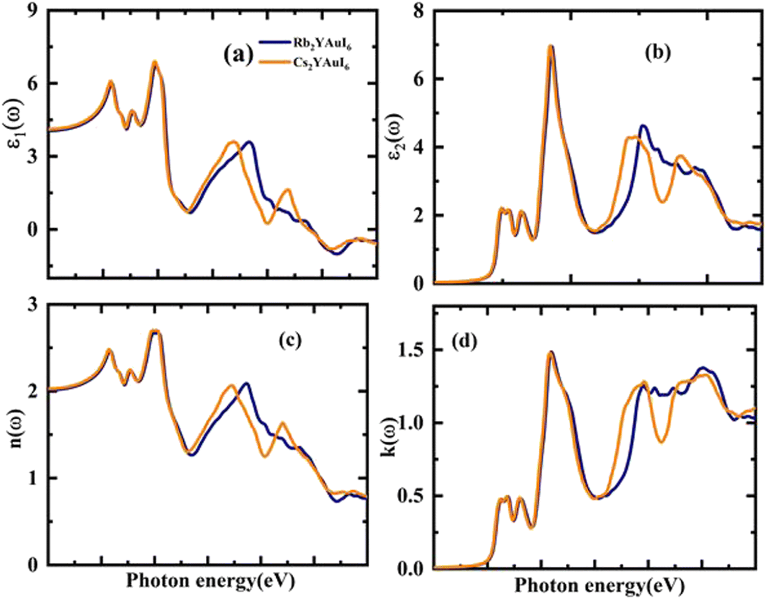 | ||
| Fig. 7 The calculated energy-dependent optical parameters: (a) real part of the dielectric function, (b) imaginary part of the dielectric function, (c) refractive index coefficient, and (d) extinction coefficient of A2YAuI6 (A = Rb, Cs). | ||
The imaginary portion is indicated as,
 | (7) |
Possible light-energy absorptions leading to an inter-band transition have been associated with ε2(ω). This can be seen in Fig. 7(b), where the visible portions of the two computed compounds are the primary focus of the light absorptions. Cs2YAuI6 has a smaller bandgap that polarizes electron transfer in the conductance band and improves the photovoltaic outcomes. The methodical examination of ε1(ω) and ε2(ω) revealed that Rb2YAuI6 and Cs2YAuI6 have shown sufficient energy to absorb light in the broad range of wavelengths from 2–5 eV. Fig. 7(c and d) displays the complex refractive index. The real part of n(ω) in any medium of electromagnetic wave (EM) is the measurement of the phase velocity. Additionally, the imaginary component k(ω) arises as a result of an electromagnetic wave propagating through the same medium. The calculated static value n(0) has been observed at 2.01 and 2.03 for Rb2YAuI6 and Cs2YAuI6, respectively. The imaginary k(ω) and real n(ω) components of the maximum estimated values for Rb2YAuI6 are observed at 2.47 eV and 2.64 eV, respectively. Upon converting the composition to Cs2YAuI6, these values changed to 1.48 eV and 2.66 eV, respectively. When some halides are exposed to a specific frequency of photon radiation, the electrons begin to condense.
The electronic conduction causes this optical conductivity (σ(ω)), which is depicted in Fig. 8(a). The first peak of σ(ω) has been observed for Rb2YAuI6 at 718 (ω cm)−1 at 2.54 eV, and the highest value of conductivity is found at 4772 (ω cm)−1 at 7.68 eV. On the other hand, the first peak of 721 at 2.21 eV with a maximum conductivity is 4533 at 9.12 eV for Cs2YAuI6.
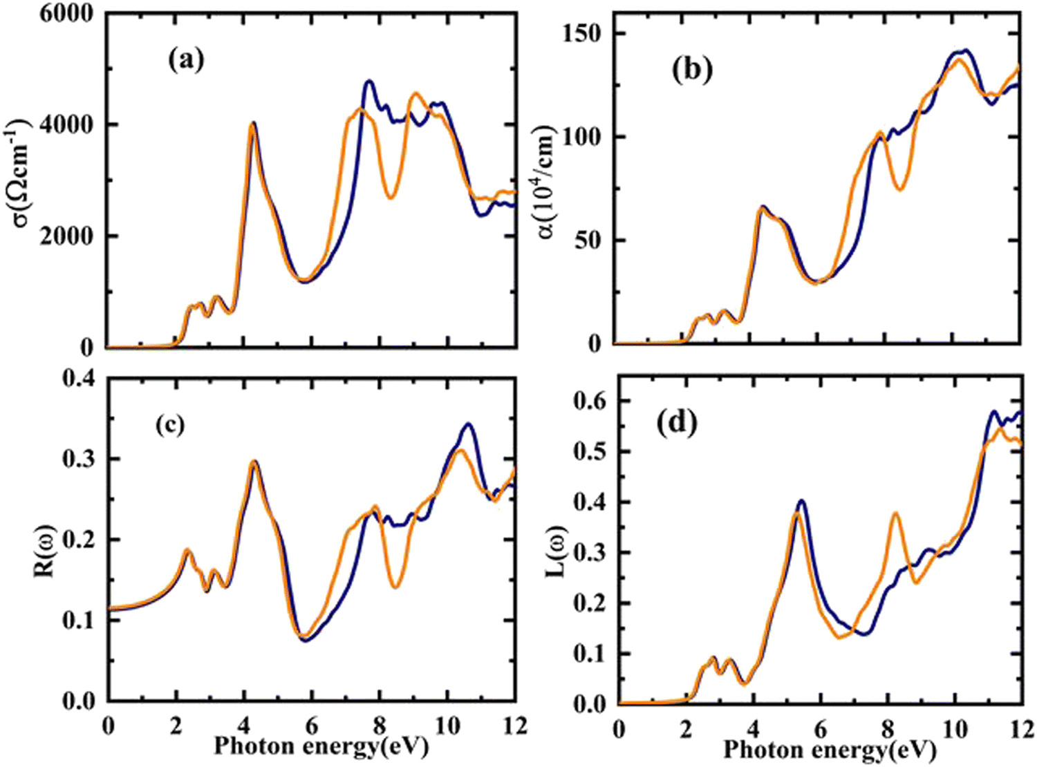 | ||
| Fig. 8 The calculated energy-dependent optical parameters: (a) optical conductivity, (b) absorption coefficient, (c) optical reflectivity, and (d) energy loss function of A2YAuI6 (A = Rb, Cs). | ||
The distance is measured prior to the absorption of light at a particular frequency. It is clear that the absorption coefficient spectrum α(ω) for Rb2YAuI6 begins at 2.21 eV and peaks at 10.54 eV as s displaced in Fig. 8(b). However, for Cs2YAuI6, α(ω) begins at 2.20 eV and reaches its maximum value at 10.20 eV. When the approaching photons reach the absorption edge, a dramatic increase in the absorption coefficient values is also noticed. Meanwhile, the optical absorptions of Cs2LiGaI6 and Rb2LiGaI6 have their initial maximum absorption bands and conductivity peaks in the visible energy band of (2.8–3.0 eV) and (2.65–2.8 eV), respectively.27 It has been observed that our examined compounds can absorb electromagnetic radiation from the (UV-visible) region with wavelengths of 119–562 nm for Rb2YAuI6 and 122–565 nm for Cs2YAuI6, as shown in Fig. 8(b). This further supports the validity of these materials in the solar energy industry. The results of the optical absorption show that both compounds can absorb a wide UV-visible range of electromagnetic radiation in accordance with their electronic behavior, making it a potential candidate for optoelectronic and solar cell applications.
Similar to the previous discussion of optical parameters, the reflectivity R(ω) and optical loss L(ω) are significant variables, and their values should be low for the best optical materials. The surface morphology of the studied compounds is depicted by R(ω). The computed R(ω) values are displayed in Fig. 8(c). For Rb2YAuI6 and Cs2YAuI6, their values at zero energy are 0.113 and 0.115, respectively. The maximum value of reflectivity has been observed at 10.62 eV (0.34) and 10.38 eV. The light scattering and dispersion are displaced in Fig. 8(d), as illustrated by L(ω). It is worth mentioning that minimal energy loss has been observed in the visible region, which shows that these materials are suitable for solar cell applications.
6. Thermoelectric properties
Based on the figure of merit (ZT) provided by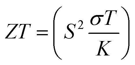 ,51–53 we have evaluated the thermoelectric efficiency of our examined compounds. The enhanced Seebeck coefficient (S), higher electrical conductivity (σ), and lowered thermal conductivity (κ) describe an effective thermoelectric compound. For Rb2YAuI6 and Cs2YAuI6, we have calculated their thermoelectric properties in relation to the temperature T (K), chemical potential μ (eV) and carrier concentration N (e/u.c) using the Boltztrap code.36 All calculated transport parameters at room temperature, i.e., 300 K, are tabulated in Table 5.
| Material property | Rb2YAuI6 | Cs2YAuI6 | |
|---|---|---|---|
| Transport properties (300 K) | σ/τ (1018 Ω−1 m−1 s−1) | 9.14 | 8.68 |
| S (μV K−1) | 207 | 212 | |
| R H (10−8 m3 C−1) | 1.96 | 2.04 | |
| κ e (1014 W m−1 K−1 s−1) | 1.57 | 1.53 | |
| S 2 σ/τ (1011 W K−2 m−1 s−1) | 3.93 | 3.89 |
The carrier's concentration has been used to classify the p and n-type features. The energy required to add or remove electrons from the material is indicated by μ. When electrons are introduced into the system, μ is positive. When they are taken out of the system, the μ is negative. The system operates as an n-type material when electrons are introduced. When electrons are removed, the system becomes more hole-filled, indicating that the materials under study are p-type.54 Additionally, Fig. 4 shows that the DOS are more heavily occupied in the valence band than in the conduction band, confirming the p-type character of holes and their function as dominating charge carriers. The possibility that carriers will exist is represented by the density of states. Compared to the conduction band, the valence band contains a higher density of closely spaced states, indicating that there are more carriers available there. In semiconductors, the behavior becomes p-type if there are more holes (VB) than electrons (CB).
The Seebeck coefficient (S) may be expressed as S = ΔV/ΔT, where ΔT denotes the temperature gradient. The Seebeck coefficient is the material's capacity to produce induced emf when a temperature differential is applied. Fig. 9(a) displays the computation of the Seebeck coefficient (S) alongside T. As the temperature rises, the value of S decreases. For two complexes, the value of S is positive, indicating that the majority of the charge carriers in those materials are holes. The calculated values of S at room temperature are 207.3 μV K−1 (Rb2YAuI6) and 211.6 μV K−1 (Cs2YAuI6). Fig. 9(b) shows the Seebeck coefficient for the given material at different Kelvin temperatures versus chemical potential. It is clear that the Seebeck coefficient shows distinct peaks and slopes over the whole chemical potential range.
 | ||
| Fig. 9 Variation of the band structures of A2YAuI6 (A = Rb, Cs) with temperature using TB-mBJ approximation: (a) Seebeck coefficients, (b) and (c) Seebeck coefficients against chemical potential, (d) electrical conductivity, (e) and (f) electrical conductivity versus chemical potential. | ||
The chemical potential of the p-type region has the highest value, 2925 μV K−1 for (Rb2YAuI6) and 2897 μV K−1 for (Cs2YAuI6) at room temperature. The chemical in consideration exhibits a greater Seebeck coefficient value due to its large band gap and restricted carrier mobility. However, at higher temperatures, S is somewhat dropped to 719 μV K−1 and 708 μV K−1 for Rb2YAuI6 and Cs2YAuI6, respectively. The bipolar effect, which continues when bound electrons are propelled by thermal energy and create electron–hole pairs, is responsible for the drop in the Seebeck coefficient at higher temperatures. These findings entirely agree with the Mott relationship, which measures how much temperature and chemical potential influence the Seebeck coefficient.55 The current material may find application in temperature sensors, thermocouples, thermoelectric coolers, and generators due to its non-zero value of S at high temperatures.
The material flow is caused by electronic movement (kel) and lattice vibration (kph), which also results in thermal conductivity (ke/τ).56 Electrons are triggered by elastic waves produced by lattice vibration. Therefore, when estimating the electronic component of ke/τ, we ignored the phononic element of the thermal conductivity. Fig. 9(c) shows the thermal conductivity against the chemical potential, while Fig. 9(d) shows the behavior of the thermal conductivity against temperature. The ke/τ rises as the temperature rises because a higher temperature increases the carrier mobility, which in turn improves the electronic movement and raises the electronic thermal conductivity.
The electrical conductivity (σ/τ) versus chemical potential m (eV) is represented in Fig. 10(b and c), whereas the electrical conductivity versus temperature (K) is shown in Fig. 10(a). The chemical potential, whose value is 0 at the Fermi level, is the necessary amount of energy to get the electrons included in the circuit for overcoming the Coulomb potential. The chemical potential could either have a positive or negative value. The p-type behavior is expressed by the negative value, and the n-type reaction is represented by the positive value.57,58 A greater number of conduction electrons are present at high energies, as indicated by the high values of σ/τ between 0 and −0.7 and −0.8 eV for Rb2YAuI6 and Cs2YAuI6, respectively. The σ/τ peak for Rb2YAuI6 indicates a large intensity (which means it includes more conduction electrons than Cs2YAuI6), which is in accordance to previous studies.24
 | ||
| Fig. 10 Variation of the band structures of A2YAuI6 (A = Rb, Cs) with temperature using TB-mBJ approximation: (a) electronic thermal conductivity, (b) and (c) electronic thermal conductivity against chemical potential, (d) power factor, (e) and (f) power factor versus chemical potential. | ||
The power factor (S2σ/τ) computed to guess the thermoelectric strength of the examined compounds versus temperature and chemical potential is displayed in Fig. 10(a and b). As the temperature rises, the power factor increases linearly, as demonstrated by the sharp decline in the value of the Seebeck coefficient depicted in Fig. 9(a).
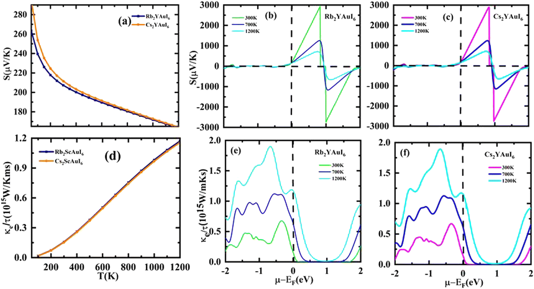
A factor known as the figure of merit is in charge of the compound thermoelectric activity. Furthermore, by dividing the power factor by thermal conductivity, this factor is used to calculate the true thermoelectric efficiency.51ZT alongside temperature (T) is displayed in Fig. 11(a), and also against the chemical potential, as shown in Fig. 11(b and c) respectively. The maximum value of ZT is 0.98 at the chemical potential value of 0.48 eV for Rb2YAuI6 and 0.99 at 0.50 eV for Cs2YAuI6 at room temperature, 300 K. In other studies, the value of ZT decreased with the rise in temperature.24 As a result, the compounds under study exhibit a high ZT at room temperature. The description above makes clear how crucial the analysis is for thermoelectric generators and other thermoelectric functions.
 | ||
| Fig. 11 The computed results of figure of merit by Tb-mBJ (a) ZT against temperature, (b) and (c) ZT versus chemical potential. | ||
The Seebeck coefficients S and σ/τ versus N (e/u.c) with positive and negative doping in the materials are shown in Fig. 12(a–d). Increasing the doping and temperature (K) and σ/τ do not alter the graphs of the Seebeck coefficient. Thus, as illustrated in Fig. 12(a and b), we found that the Cs2YAuI6 molecule exhibits a significant variance in p-type doping from 0 to 0.2. Furthermore, for both compounds under study, a maximum accomplishment in σ/τ is observed at 1.1 N (e/u.c). The electronic thermal conductivity (ke/τ) of the explored composites has been calculated in order to investigate the heat energy created by the materials. We investigated these materials against n-type and p-type doping at temperatures of 300, 700, and 1200 K. The electronic conductivity is presented in Fig. 13(a and b) against the carrier concentration. For the Rb2YAuI6 compound, we managed to achieve the maximum value at 300, 700, and 1200 K, which is 0.51 × 10¹⁵ W m−1 K−1 s−1, 0.90 × 10¹⁵ W m−1 K−1 s−1 at −1.1 N (e/u.c) and 1.05 × 10¹⁵ at −1.86 N (e/u.c). Similarly, Cs2YAuI6 has values at 300, 700, and 1200 with 0.50 × 10¹⁵ W m−1 K−1 s−1, 0.87 × 10¹⁵ W m−1 K−1 s−1 at −1.1 N (e/u.c), and 1.02 × 10¹⁵ at −1.86 N (e/u.c).
 | ||
| Fig. 12 Accomplished thermoelectric properties (a, b) S and (c, d) σ/τ against the carrier concentration of A2YAuI6 (A = Rb, Cs) using the TB-mBJ approximation. | ||
 | ||
| Fig. 13 Accomplished thermoelectric properties (a, b) κe/τ and (c, d) PF against the carrier concentration of A2YAuI6 (A = Rb, Cs) using the TB-mBJ approximation. | ||
The PF for both double perovskites is shown in Fig. 13(c and d) at various temperatures, including 300, 700, and 1200 K at 1 N (e/u.c). For n-type doping, there is no PF, but both materials achieve values close to the Fermi level at 1200 K, which is 7.44 × 10¹¹ and 7.40 × 10¹¹ W m−1 K−2 s−1 for Rb2YAuI6 and Cs2YAuI6, respectively.
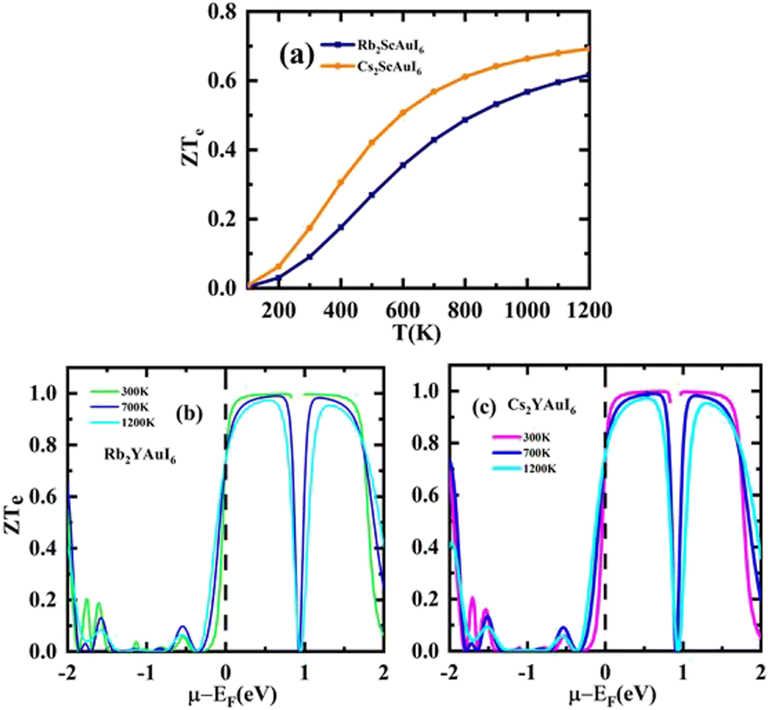
Fig. 14(a and b) shows that for both compounds under study, the ZT values at 0 N (e/u.c) are 1, but that the ZT values sharply decline with increasing p-type doping and linearly decrease with increasing n-type doping.
 | ||
| Fig. 14 Calculated thermoelectric properties figure of merit ZT against the carrier concentration of (a) Rb2YAuI6, (b) Cs2YAuI6 using TB-mBJ approximation. | ||
7. Conclusion
In our study, we computed the opto-electronic and thermoelectric features of A2YAuI6 (A = Rb, Cs) using DFT calculations. The PBE generalized gradient approximation has been implemented to optimize the structural parameters. In order to acquire appropriate energy band gaps, Tb-mBJ with and without SOC schemes were used instead of PBE-GGA. It has been established that Rb2YAuI6 is more ductile than Cs2YAuI6 due to its higher Pugh's and Poisson's ratio values. The materials have indirect bandgaps of 1.73 and 1.70 eV for Rb2YAuI6 and Cs2YAuI6, respectively, which are potential materials for the manufacturing of solar cell devices and lie in the UV-visible region of the EM spectrum. The negative values of the formation energy and tolerance factor show that the examined materials are thermodynamically stable. The ELF plots demonstrate that there is an ionic connection between Rb/CS, I, and Au. The solar cells are favored by the lowest values of optical loss and reflection, combined with significant visible light attenuation. Thermoelectric generator applications benefit greatly from the huge values of ZT, Seebeck coefficient, and PF at low temperatures of 300 K, as well as the ultralow value of the lattice vibration. As a result, these compounds will provide the experimental community with profound insight into how to implement them to advance the solar cell and thermoelectric generator industries.Conflicts of interest
There are no conflicts to declare.Acknowledgements
M. M. is supported by APVV-21-0272, VEGA-2/0070/21 Project, Slovakia.References
- J. Chen, X. Cai, D. Yang, D. Song, J. Wang and J. Jiang, et al., Recent progress in stabilizing hybrid perovskites for solar cell applications, J. Power Sources, 2017, 355, 98–133 CrossRef CAS.
- M. J. Fang, C. W. Tsao and Y. J. Hsu, Semiconductor nano-hetero structures for photo-conversion applications, J. Phys. D: Appl. Phys., 2020, 53, 143001 CrossRef CAS.
- S. Choudhary, A. Shukla, J. Chaudhary and A. S. Verma, Extensive investigation of structural, electronic, optical, and thermoelectric properties of hybrid perovskite (CH3NH3PbBr3) with mechanical stability constants, Int. J. Energy Res., 2020, 44, 11614–11628 CrossRef CAS.
- Y. Saeed, B. Amin, H. Khalil, F. Rehman, H. Ali and M. I. Khan, et al., Cs2NaGaBr6: a new lead-free and direct band gap halide double perovskite, RSC Adv., 2020, 10, 17444–17451 RSC.
- Y. Jia, Y. Zeng, X. Li and L. Meng, Effect of Sr substitution on the property and stability of CH3NH3SnI3 perovskite: a first principles investigation, Int. J. Energy Res., 2020, 44, 5765–5778 CrossRef CAS.
- R. Kour, S. Arya, S. Verma, J. Gupta, P. Bandhoria and V. Bharti, et al., Potential substitutes for replacement of lead in perovskite solar cells: a review, Global Challenge, 2019, 3, 1900050 CrossRef PubMed.
- D. Zhou, T. Zhou, Y. Tian, X. Zhu and Y. Tu, Perovskite-based solar cells: materials, methods, and future perspectives, J. Nanomater., 2018, 2018, 8148072 Search PubMed.
- M. Palummo, E. Berrios, D. Varsano and G. Giorgi, Optical properties of lead-free double perovskites by ab initio excited-state methods, ACS Energy Lett., 2020, 5, 457–463 CrossRef CAS.
- G. Volonakis, A. A. Haghighirad, R. L. Milot, W. H. Sio, M. R. Filip and B. Wenger, et al., Cs2InAgCl6: a new lead-free halide double perovskite with direct band gap, J. Phys. Chem. Lett., 2017, 8, 772–778 CrossRef CAS.
- B. K. Ghosh and T. K. Biswas, Emerging solar cells energy trade-off: interface engineering materials impact on stability and efficiency progress, Int. J. Energy Res., 2019, 43, 1670–1688 CrossRef CAS.
- C. Shi, J. J. Ma, J. Y. Jiang, M. M. Hua, Q. Xu and H. Yu, et al., Large piezoelectric response in hybrid rare-earth double perovskite relaxor ferroelectrics, J. Am. Chem. Soc., 2020, 142, 9634–9641 CAS.
- C. C. Stoumpos, C. D. Malliakas and M. G. Kanatzidis, Semiconducting tin and lead iodide perovskites with organic cations: phase transitions, high mobilities, and near-infrared photoluminescent properties, Inorg. Chem., 2013, 52, 9019–9038 CrossRef CAS.
- N. K. Noel, S. D. Stranks, A. Abate, C. Wehrenfennig, S. Guarnera and A. A. Haghighirad, et al., Lead-free organiceinorganic tin halide perovskites for photovoltaic applications, Energy Environ. Sci., 2014, 7, 3061–3068 RSC.
- F. Hao, C. C. Stoumpos, D. H. Cao, P. R. Chang and M. G. Kanatzidis, Lead-free solid-state organiceinorganic halide perovskite solar cells, Nat. Photonics, 2014, 8, 489–494 CrossRef CAS.
- C. C. Stoumpos, C. D. Malliakas, J. A. Peters, Z. Liu, M. Sebastian and J. Im, et al., Crystal growth of the perovskite semiconductor CsPbBr3: a new material for high-energy radiation detection, Cryst. Growth Des., 2013, 13, 2722–2727 CrossRef CAS.
- M. Kulbak, D. Cahen and G. Hodes, How important is the organic part of lead halide perovskite photovoltaic cells? Efficient CsPbBr3 cells, J. Phys. Chem. Lett., 2015, 6, 2452–2456 CrossRef CAS PubMed.
- M. Kulbak, S. Gupta, N. Kedem, I. Levine, T. Bendikov and G. Hodes, et al., Cesium enhances long-term stability of lead bromide perovskite-based solar cells, J. Phys. Chem. Lett., 2016, 7, 167–172 CrossRef CAS PubMed.
- E. T. McClure, M. R. Ball, W. Windl and P. M. Woodward, Cs2AgBiX6 (X¼ Br, Cl): new visible light absorbing, lead-free halide perovskite semiconductors, Chem. Mater., 2016, 28, 1348–1354 CrossRef CAS.
- T. Wang, D. Yue, X. Li and Y. Zhao, Lead-free double perovskite Cs2AgBiBr6/RGO composite for efficient visible light photo catalytic H2 evolution, Appl. Catal., B, 2020, 268, 118399 CrossRef CAS.
- S. R. Bhandari, D. K. Yadav, B. P. Belbase, M. Zeeshan, B. Sadhukhan and D. P. Rai, et al., Electronic, magnetic, optical and thermoelectric properties of Ca2Cr1x NixOsO6 double perovskites, RSC Adv., 2020, 10, 16179–16186 RSC.
- C. C. Sorrell, S. Sugihara and J. Nowotny, Materials for energy conversion devices, Woodhead Pub. Limited, 2005, vol. 416 Search PubMed.
- E. Haque and M. A. Hossain, Electronic, phonon transport and thermoelectric properties of Cs2InAgCl6 from first-principles study, Comput. Condensed Matter, 2019, 19, 00374 Search PubMed.
- M. Aslam Khan, H. A. Alburaih, N. A. Noor and A. Dahshan, Comprehensive investigation of Opto-electronic and transport properties of Cs2ScAgX6 (X ¼ Cl, Br, I) for solar cells and thermoelectric applications, Sol. Energy, 2021, 225, 122–128 CrossRef CAS.
- N. A. Noor, M. W. Iqbal, T. Zelai, A. Mahmood, H. M. Shaikh, S. M. Ramay and W. Al Masry, Analysis of direct band gap A2ScInI6 (A ¼ Rb, Cs) double perovskite halides using DFT approach for renewable energy devices, J. Mater. Res. Technol., 2021, 13, 2491–2500 CrossRef CAS.
- S. Iqbal, G. M. Mustafa, M. Asghar, N. A. Noor, M. W. Iqbal, A. Mahmood and Y. H. Shin, Tuning the optoelectronic and thermoelectric characteristics of narrow bandgap Rb2AlInX6 (X¼ Cl, Br, I) double perovskites: a DFT study, Mater. Sci. Semicond. Process., 2022, 143, 106551 CrossRef CAS.
- R. Anbarasan, M. Srinivasan, R. Suriakarthick, H. Albalawi, J. K. Sundar, P. Ramasamy and Q. Mahmood, Exploring the structural, mechanical, electronic, and optical properties of double perovskites of Cs2AgInX6 (X ¼ Cl, Br, I) by first principles calculations, J. Solid State Chem., 2022, 310, 123025 CrossRef CAS.
- S. Nazir, N. A. Noor, M. Manzoor and A. Dahshan, Ab-initio simulations of Li-based Double Perovksites A2LiInBr6 (A ¼ Rb, Cs) for solar cell applications, Chem. Phys. Lett., 2022, 798, 139612 CrossRef CAS.
- P. Blaha, K. Schwarz, G. K. H. Madsen, D. Kvasnicka and J. Luitz, Techn. An Augmented Plane Wave+ Local Orbitals Program for Calculating Crystal Properties, 2001 Search PubMed.
- K. Schwarz, P. Blaha and G. K. H. Madsen, Electronic structure calculations of solids using the WIEN2k package for material sciences, Comput. Phys. Commun., 2002, 147, 71 CrossRef.
- M. Petersen, F. Wagner, L. Hufnagel, M. Scheffler, P. Blaha and K. Schwarz, Improving the efficiency of FP-LAPW calculations, Comput. Phys. Commun., 2000, 126, 294–309 CrossRef CAS.
- J. P. Perdew, A. Ruzsinszky, G. I. Csonka, O. A. Vydrov, G. E. Scuseria, L. A. Constantin, X. Zhou and K. Burke, Restoring the density-gradient expansion for exchange in solids and surfaces, Phys. Rev. Lett., 2008, 100, 136406 CrossRef PubMed.
- J. P. Perdew, K. Burke and M. Ernzerhof, Generalized gradient approximation made simple, Phys. Rev. Lett., 1996, 77, 3865 CrossRef CAS PubMed.
- F. Tran and P. Blaha, Accurate band gaps of semiconductors and insulators with a semilocal exchange–correlation potential, Phys. Rev. Lett., 2009, 102, 226401 CrossRef PubMed.
- J. P. Perdew, K. Burke and M. Ernzerhof, Generalized gradient approximation made simple, Phys. Rev. Lett., 1996, 77, 3865–3868 CrossRef CAS PubMed.
- P. E. Blöchl, O. Jepsen and O. K. Andersen, Improved tetrahedron method for Brillouin-zone integrations, Phys. Rev. B: Condens. Matter Mater. Phys., 1994, 49, 16223 CrossRef PubMed.
- G. K. Madsen and D. J. Singh, BoltzTraP. A code for calculating band structure dependent quantities, Comput. Phys. Commun., 2006, 175, 67–71 CrossRef CAS.
- F. Birch, Finite elastic strain of cubic crystals, Phys. Rev., 1947, 71(11), 809 CrossRef CAS.
- Alexander E. Fedorovskiy, A. Drigo Nikita and Mohammad KhajaNazeeruddin, The role of Goldschmidt's tolerance factor in the formation of A2BX6 double halide perovskites and its optimal range, Small Methods, 2020, 4(5), 1900426 CrossRef CAS.
- Q. Mahmood, T. Ghrib, A. Rached, A. Laref and M. A. Kamran, Probing of mechanical, optical and thermoelectric characteristics of double perovskites Cs2GeCl/Br6 by DFT method, Mater. Sci. Semicond. Process., 2020, 112, 105009 CrossRef CAS.
- M. Roknuzzaman, K. K. Ostrikov, H. Wang, A. Du and T. Tesfamichael, Towards lead-free perovskite photovoltaics and optoelectronics by ab-initio simulations, Sci. Rep., 2017, 7, 14025 CrossRef PubMed.
- Y. O. Ciftci, K. Colakoglu, E. Deligoz and H. Ozisik, The first principles study on the LaN, Mater. Chem. Phys., 2008, 108, 120–123 CrossRef CAS.
- Y. J. Hao, X. R. Chen, H. L. Cui and Y. L. Bai, First-principles calculations of elastic constants of c-BN, Phys. B, 2006, 382, 118–122 CrossRef CAS.
- M. Marathe, A. Gru
![[n with combining umlaut]](https://www.rsc.org/images/entities/char_006e_0308.gif) ebohm, T. Nishimatsu, P. Entel and C. Ederer, First-principles-based calculation of the electrocaloric effect in BaTiO3: a comparison of direct and indirect methods, Phys. Rev. B, 2016, 93, 054110 CrossRef.
ebohm, T. Nishimatsu, P. Entel and C. Ederer, First-principles-based calculation of the electrocaloric effect in BaTiO3: a comparison of direct and indirect methods, Phys. Rev. B, 2016, 93, 054110 CrossRef. - E. A. Khera, U. Rasheed, M. Imran, H. Ullah, F. Hussain, R. A. Khalil and M. Qasim, An insight into structural, electronic and optical characteristics of Mo1-xMxO3 (M= Zr, Y, ZrY) for the formation of conducting filaments in optoelectronic memory devices: A first principles study, Optik, 2022, 258, 168913 CrossRef CAS.
- Y. Saeed, B. Amin, H. Khalil, F. Rehman, H. Ali and M. I. Khan, et al., Correction: Cs2NaGaBr6: a new lead-free and direct band gap halide double perovskite, RSC Adv., 2020, 10, 20196 RSC.
- R. Ahmed, N. S. Masuri, B. U. Haq, A. Shaari, S. AlFaifi, F. K. Butt and S. A. Tahir, Investigations of electronic and thermoelectric properties of half-Heusler alloys XMgN (X= Li, Na, K) by first-principles calculations, Mater. Des., 2017, 136, 196–203 CrossRef CAS.
- E. A. Khera, U. Rasheed, M. Imran, H. Ullah, F. Hussain, R. A. Khalil and M. Qasim, An insight into structural, electronic and optical characteristics of Mo1-xMxO3 (M= Zr, Y, ZrY) for the formation of conducting filaments in optoelectronic memory devices: A first principles study, Optik, 2022, 258, 168913 CrossRef CAS.
- M. H. Samat, A. M. M. Ali, M. F. M. Taib, O. H. Hassan and M. Z. A. Yahya, Hubbard U calculations on optical properties of 3d transition metal oxide TiO2, Results Phys., 2016, 6, 891–896 CrossRef.
- P. Puschnig and C. Ambrosch-Draxl, Phys. Rev. B, 2020, 66, 165105 CrossRef.
- D. R. Penn, Wave-number-dependent dielectric function of semiconductors, Phys. Rev., 1962, 128, 2093 CrossRef CAS.
- H. C. Wang, P. Pistor, M. A. L. Marques and S. Botti, Double perovskites as p-type conducting transparent semiconductors: a high-throughput search, J. Mater. Chem., 2019, 7, 14705 RSC.
- Q. Mahmood, T. Zelai, T. Usman, S. Al-Qaisi, M. Morsi, H. Albalawi, A. I. Aljameel, O. A. Alamri and G. Murtaza, First-principles study of lead-free double perovskites K2Pt(Cl/Br)6 for optoelectronic and renewable energy applications, J. Solid State Chem., 2021, 301, 122294 CrossRef CAS.
- T. H. Flemban, V. Singaravelu, A. A. S. Devi and I. S. Roqan, Homogeneous vertical ZnOnanorod arrays with high conductivity on an in situ Gd nanolayer, RSC Adv., 2015, 5(115), 94670–94678 RSC.
- Q. Mahmood, M. H. Alhossainy, M. S. Rashid, T. H. Flemban, H. Althib, T. Alshahrani, M. Rashid and A. Laref, First-principles study of lead-free double perovskites Rb2TeX6 (X ¼Cl, Br, and I) for solar cells and renewable energy, Mater. Sci. Eng. B, 2021, 266, 115064 CrossRef CAS.
- M. Jonson and G. D. Mahan, Phys. Rev. B: Condens. Matter Mater. Phys., 1980, 21, 4223–4229 CrossRef CAS.
- J. P. Heremans, V. Jovovic, E. S. Toberer, A. Saramat, K. Kurosaki and A. Charoenphakdee, et al., Enhancement of thermoelectric efficiency in PbTe by distortion of the electronic density of states, Science, 2008, 321, 554–557 CrossRef CAS PubMed.
- M. Bilal, M. Shafiq, B. Khan, H. R. Aliabad, S. J. Asadabadi and R. Ahmad, et al., Antiperovskite compounds SbNSr3 and BiNSr3: potential candidates for thermoelectric renewable energy generators, Phys. Lett., 2015, 379, 206–210 CrossRef CAS.
- F. Kim, B. Kwon, Y. Eom, J. E. Lee, S. Park and S. Jo, et al., 3D printing of shape-conformable thermoelectric materials using all inorganic Bi2Te3-based inks, Nat. Energy, 2018, 3, 301–309 CrossRef CAS.
| This journal is © The Royal Society of Chemistry 2024 |