
Strategies for suppressing dark current of perovskite photodiodes towards reliable optoelectronic applications
Yue
Wang
 *a,
Qing
Song
a,
Deli
Li
*a,
Yang
Liu
a,
Yang
Wang
a and
Yonghua
Chen
*b
*a,
Qing
Song
a,
Deli
Li
*a,
Yang
Liu
a,
Yang
Wang
a and
Yonghua
Chen
*b
aStrait Institute of Flexible Electronics (SIFE, Future Technologies), Fujian Key Laboratory of Flexible Electronics, Fujian Normal University and Strait Laboratory of Flexible Electronics (SLoFE), Fuzhou, 350117, China. E-mail: ifeywang@fjnu.edu.cn; ifedlli@fjnu.edu.cn
bKey Laboratory of Flexible Electronics (KLOFE) & Institute of Advanced Materials (IAM), Jiangsu National Synergistic Innovation Center for Advanced Materials (SICAM), Nanjing Tech University (NanjingTech), 30 South Puzhu Road, Nanjing 211816, Jiangsu, China. E-mail: iamyhchen@njtech.edu.cn
First published on 8th July 2024
Abstract
Photodetection is crucial for advancements in next-generation technologies, including Internet of Things, intelligent perception, augmented and virtual reality, and human–machine interactions. Metal halide perovskites (MHPs) show unique properties that allow for the creation of straightforward diode structures, enabling efficient photogeneration and charge collection across a broad spectrum of wavelengths, from ionizing radiation to near-infrared. However, the presence of dark current (Id) poses a significant challenge, affecting the performance of these devices. This review commences by outlining the essential performance measures impacted either directly or indirectly by Id. Subsequently, it investigates the adjustable MHP materials employed in photodiodes, with a focus on their structural and morphological characteristics. We then explore the origins of Id and highlight the crucial factors that impact the performance of MHP-based photodiodes (MHPPDs). Additionally, we examine various strategies to mitigate Id, thereby improving device efficacy. Finally, we provide insights into future directions for reducing Id in MHPPDs, potentially leading to further enhancements in photodetection technologies.
 Yue Wang | Yue Wang completed his BSc in Applied Physics from Tiangong University in 2012 and his PhD in Optical Engineering from Beijing Jiaotong University in 2018. He then worked as a postdoctoral fellow focusing on organic and perovskite-based photodetectors at the MIIT Key Laboratory of Flexible Electronics, Northwestern Polytechnical University until 2020. Currently, he is an associate professor at the Strait Laboratory of Flexible Electronics (SLoFE) and Fujian Normal University, specializing in perovskite optoelectronics and flexible electronics applications. |
1. Introduction
Photodetection is crucial in diverse fields, including medical X-ray imaging, visible light capture, near-infrared medical imaging, short-wave infrared surveillance, and machine vision.1,2 These applications fundamentally depend on semiconductor photodetectors to transduce photons into electrical signals for processing, image reconstruction, and storage. Commonly, photodiodes and phototransistors constructed from inorganic semiconductors of silicon or III–V compounds, when integrated with thin-film transistors (TFTs) or complementary metal oxide semiconductors (CMOS) within a backplane architecture, enable the creation of intricate image sensor arrays suitable for modern optoelectronics.3,4The escalating demands of Internet of Things, intelligent perception, augmented and virtual reality, and human–machine interactions necessitate components that are lightweight, energy-efficient, miniature, and mechanically flexible.5 In response, researchers are exploring diverse semiconductor-based photodetectors,6,7 including organic materials, inorganic nanocrystals (NCs), quantum dots (QDs), and metal–halide perovskites (MHPs). MHPs, in particular, have attracted substantial attention due to their remarkable capabilities. These materials offer an ultra-broad spectral photodetection range, from ionizing radiation to near-infrared, achievable through tailored adjustments in their organic and inorganic compositions. MHPs are not only derived from abundant resources and require low deposition temperatures but also form efficient single layers owing to their low exciton binding energy.8 When integrated into optoelectronic systems, they substantively augment functionality and precision in various sensing applications, such as photoplethysmography (PPG) sensors and pulse oximeters, enabling real-time and non-invasive monitoring.
While MHP-based photoconductors and phototransistors are notable for their impressive responsivity, facilitating signal amplification across applications, they tend to have slower response times and usually require additional biasing circuits for optimal performance. These factors demand careful consideration, particularly in the context of specific applications. Despite these challenges, the intrinsic properties of MHPs support the creation of simplified diode architectures that promote efficient photogeneration and charge collection with minimal losses. MHPPDs, employing configurations such as P–N, P–I–N, or Schottky junctions, can function without an external power supply. Applying an additional reverse bias can further enhance the efficiency of photogenerated carrier collection.9 Moreover, the progress in MHP-based devices benefits extensively from ongoing research on perovskite photovoltaics. Consequently, significant research efforts are directed at advancing our understanding of materials, device architectures, physical mechanisms, and processing techniques in this field. This endeavor seeks to improve the figures of merits (FOMs) of MHPPDs to bring them on par with those of their counterparts.
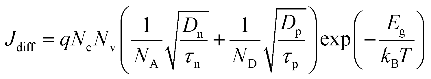
A critical parameter affecting MHPPDs' FOMs directly or indirectly, including the on–off ratio (OOR), linear dynamic range (LDR), specific detectivity (D*), is the dark current (Id). In MHPPDs, as illustrated in Fig. 1, carriers in an MHP film tend to drift towards their respective electrodes in the absence of a bias voltage. This behavior, facilitated by the unique properties of MHPs, leads to complete depletion even without an applied bias voltage, significantly impacting the device's performance. The OOR is defined as the ratio of the photocurrent generated when the photodiode is exposed to light (on-state) to Id when it is not exposed to light (off-state). This ratio indicates how effectively a photodiode can distinguish between the presence and absence of light signals. Therefore, reducing Id in MHPPDs while preserving the photocurrent can considerably enhance the OOR. The LDR represents a valuable feature for MHPPDs where the output, such as photocurrent or responsivity, remains stable across a broad spectrum of incident light intensities. Beyond this dynamic range, the light signals cannot be accurately detected due to the elevated levels of Id.10 Additionally, the noise equivalent power (NEP) defines the minimum optical power a photodiode can differentiate from the noise current, indicating the sensitivity of the photodiode to weak light signals. Noise current (in) in units of A Hz−1/2 primarily includes shot noise, thermal noise, and flicker noise, among which shot noise, arising from the discrete passage of electrons and holes, generally dominates. Thermal noise is linked to the random motion of charge carriers, and flicker noise can result from fluctuations in conductivity due to variations in the electron concentration.11 Additionally, the influence of Id in the practical industrial applications of photodiodes is substantial. For example, high Id can rapidly reach the breakdown voltage of TFTs or CMOS, widely employed in imaging and sensing technology, rendering them ineffective.12
 | ||
| Fig. 1 Schematic illustration of the energy diagram of P–I–N photodiodes without bias (a) and under bias conditions (b). Schematic of the parameters influenced by Id in photodiodes for light sensing and direct X-ray detection. (c) On–off ratio (OOR). (d) Noise current (in). (e) Linear dynamic range (LDR). (f) Detection limit. | ||
Furthermore, the Id of MHPPDs plays a crucial role in direct radiation detection, specifically in X-ray imaging and ionizing radiation detection applications, enabling nondestructive inspection in medical, security, and scientific fields. In direct radiation X-ray detection, MHPPDs employ active layers with thicknesses up to millimeters to effectively block high-energy radiation photons, which raises the issue of less charge collection efficiency for the devices. One effective solution to overcome this challenge is operating MHPPDs at a high reverse bias, which unfortunately leads to a higher Id. It can deteriorate the detection limit (refers to the lowest level of X-ray radiation that can be reliably detected) and the dynamic range of the ionizing radiation response of a detector. Furthermore, due to their low defect formation energies, the formed defects within MHPs are prone to ion migration when subjected to an electric field. As a result, the high reverse bias applied to MHPPDs in ionizing radiation applications can trigger a saturation period lasting hours, referred to as Id drift, which affects the current long-term stability of MHPPDs, as these devices are typically operated at a specific reverse bias voltage relative to the reference Id.13 The Id drift can be calculated using:  where Ifinish and Ibegin are the final and initial dark currents, t is the test time, and E is the applied electric field.
Therefore, understanding the fundamental causes of Id in MHPPDs is crucial. By exploring the elements that influence Id, we can devise effective strategies to mitigate it, thus overcoming the challenges associated with the material composition and device architecture. Although recent literature14 provides a thorough examination of Id's origins, limitations, and countermeasures in various MHP-based detectors like photodiodes, photoconductors, and phototransistors, there remains a gap concerning the specific issues of Id in MHPPDs. Considering the significant impact of MHPPDs on the evolution of MHP-based photodetection technologies, further investigation in this area is essential. This review starts by defining the key performance metrics that are directly or indirectly influenced by Id. It then examines the tunable MHP materials used in photodiodes, emphasizing their structural and morphological properties. We then explore the sources of Id and identify the key factors influencing Id in MHPPDs. Additionally, we discuss various tactics to curb Id in these devices. Finally, we contemplate future approaches to reduce Id in MHPPDs, underlining the necessity of developing a clear understanding of Id's mechanisms and exploring new avenues for research to diminish Id effectively.
2. Figures of merits of photodiodes and their relationship with dark current
In the following section, we provide a comprehensive definition of the key performance metrics that are directly or indirectly influenced by Id, thereby enabling a clear understanding of the reported MHPPD performances. A schematic illustration of several parameters affected by Id is shown in Fig. 1. For the most relevant metrics, we highlight their definitions and mathematical expressions, as well as their relationships with Id.2.1 Signal-to-noise ratio
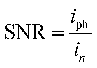
In photodiodes, the signal-to-noise ratio (SNR) is a measure of the quality of the signal relative to the level of background noise. It is defined as the ratio of the photocurrent generated by the incident light (signal) to the noise current present in the system. Mathematically, the SNR can be expressed as:where iph is the photocurrent resulting from the incident light, and in is the total noise current. Since Id contributes to the shot noise, which is a significant component of the total noise current, Id directly affects the noise current and consequently impacts the SNR. A higher Id results in increased shot noise, which reduces the SNR. Furthermore, for simplicity, the OOR is often employed to gauge the sensitivity of photodiodes to light signals. It is calculated as the ratio of the photocurrent to the Id.
2.2 Spectral responsivity and EQE
The spectral responsivity (R) in units of A W−1 describes how much current is generated by a photodiode per incoming photon of a given energy. It can be calculated using the formula:where Jph is the photocurrent density and Pin is the incident light intensity. EQE, which denotes the ratio between the number of incoming photons and the number of photogenerated free electrons, can be expressed as:

where h is the Planck constant, ν is the frequency of the incident photon, and q is the elementary charge. Generally, a high EQE (and hence R) is desirable to ensure efficient photon flux detection. In most cases, the EQE (or R) and Id are considered independent parameters. However, it is important to note that a high Id can lead to increased shot noise. This noise degrades the overall performance of the photodiode by making it more challenging to detect low-intensity signals accurately. This degradation can indirectly affect the effective EQE or (R) as well.

2.3 Speed
The speed of response, defined as the time required to collect photogenerated charge carriers at their respective contacts, ultimately determines the photodiode's dynamic range and cut-off frequency. Generally, the speed is evaluated based on the rise time (tr) (the time it takes for the device response to increase from 10% to 90%) and the fall time (tf) (the time it takes for the device response to decrease from 90% to 10%). The speed of response and Id are both dependent on the intrinsic properties of the semiconductor materials, photodiode junction capacitance, and device operating temperature. For instance, high-quality semiconductors with fewer defects typically exhibit lower Id and can also support faster response speeds. Conversely, high Id can imply higher leakage in the junction, which may increase the junction capacitance. Increased capacitance can slow down the response speed, as the photodiode takes longer to charge and discharge.2.4 Noise equivalent power and specific detectivity (D*)
The minimum incident light power that can be detected by a photodiode is referred to as the noise equivalent power (NEP). NEP is defined as the signal optical power that yields a SNR of 1. The NEP, expressed in units of W Hz−1/2, can be calculated using the formula:where in is the noise current and B is the detection bandwidth. The specific detectivity D* in units of cm Hz1/2 W−1 (or Jones) is the reciprocal of the NEP normalized to the square root of the device area A:

As discussed, in primarily comprises shot noise, thermal noise, and flicker noise. Experimental measurements of in are challenging and not always performed. For simplicity, it is often assumed that the shot noise (ishot) from the Id is the dominant contribution to in:

This assumption implies that the Id (or ishot) is the primary factor limiting D*, while thermal noise and flicker noise are ignored. However, in photodiodes, and particularly in MHPPDs, in is not solely equivalent to ishot, especially at low frequencies. Thus, this simplification can lead to an overestimation of D*.

2.5 Linear dynamic range
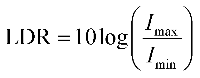
In photodiodes, the linear dynamic range (LDR) is a specification that indicates the range of incident light intensities over which the photodiode can produce a linear (proportional) response in terms of the output photocurrent. Essentially, it quantifies the operational light intensity span of the image sensor. It is defined as the ratio between the maximum detectable photocurrent before saturation and the minimum detectable photocurrent above the noise floor. Mathematically, the LDR can be expressed in decibels (dB) as:where Imax is the maximum photocurrent that the photodiode can handle linearly, limited by the onset of saturation. Imin is the minimum photocurrent that can be detected above the noise floor, dominated by the Id and other noise sources. A higher Id increases the noise floor, thus raising the minimum detectable photocurrent Imin. Consequently, this reduces the LDR because: as Imin increases, the ratio Imax/Imin decreases. This ratio determines the LDR, so an increase in Imin directly reduces the LDR.
3. Metal halide perovskites for photodiodes
Typically, MHPs have the general formula ABX3, where A represents monovalent cations such as CH3NH3+ (MA), HC(NH2)2+ (FA), cesium (Cs+), and rubidium (Rb+) or their combinations. B refers to divalent metal cations such as Pb2+, Sn2+, Bi2+, and Ge2+, while X represents halide anions such as Cl−, Br−, and I− or a combination thereof. By adjusting the components, structure, and morphology, the optical absorption and electrical properties of MHPs can be easily modified. For example, as the ionic radius of the A cation increases (rCs+ < rMA+ < rFA+), the lattice expands, and the bandgap decreases, leading to a red shift in the optical absorption band. Another way to tune the bandgap is by replacing Pb2+ with Sn2+, which reduces the bandgap and extends the optical absorption edge into the near-infrared (NIR) region. Successive tuning of the bandgap of MHPs can also be manipulated by changing the halide composition. As shown in Fig. 2a, the halide composition changes from Cl− to Br− to I−, and the bandgap sequentially decreases, allowing MHPs to absorb a broader range of light from ultraviolet (UV) to visible wavelengths.15 Furthermore, MHPs composed of Pb, Bi, I, and Br are promising for direct radiation detection due to the high atomic number of these elements, providing excellent potential for quick X-ray direct detection.16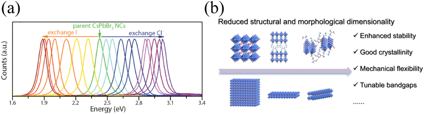 | ||
| Fig. 2 (a) Bandgaps of MHPs (CsPbBr3 nanocrystals) can be tuned by changing halide components. Reproduced with permission.17 Copyright 2015, ACS. (b) Optical and electrical properties can be tuned by the tunable dimensionality at the structural and morphological level of MHPs. Reproduced with permission.18 Copyright 2021, ACS. | ||
The structure dimensionality of MHPs can be tuned from three-dimensional (3D) bulk materials to two-dimensional (2D) layered structures and one-dimensional (1D) chain materials by manipulating the connections of [BX6]4− octahedral units (as shown in Fig. 2b). For instance, 2D MHPs are formed by incorporating larger organic cation layers between the octahedral network of 3D MHPs. This can be expressed as a general formula (LA)m(A)n−1BnX3n+1, where LA represents the larger organic cation and n denotes the number of layers in the 2D MHP structure. Introducing these larger organic cations in low-dimensional MHPs enhances their moisture stability and mechanical flexibility compared to their 3D counterparts. However, it should be noted that these long-chain organic cations also decrease the dielectric constant of MHPs, leading to an increase in the exciton binding energy. Consequently, the efficient separation and extraction of photogenerated carriers can be impeded.19
Moreover, the control over the morphology dimensionality of MHPs enables the incorporation of novel properties into these materials.20 (Fig. 2b) For instance, 0D MHP nanostructures such as NCs and QDs exhibit tunable sizes ranging from several to tens of nanometers. These nanostructures generally possess large extinction coefficients and demonstrate characteristics of multiple-exciton generation. On the other hand, 1D MHP micro/nanostructures, including nanowires (NWs) and nanorods (NRs), feature significant surface-to-volume ratios and anisotropic geometries. These attributes contribute to low defect/trap densities, prolonged charge-carrier lifetimes, and reduced carrier recombination rates. Furthermore, 2D MHPs, comprising nanoplates, nanoflakes, and nanosheets, exhibit strong quantum confinement effects and possess unique morphological characteristics. Additionally, these low-dimensional MHP materials demonstrate reasonable mechanical flexibility due to their atomic thickness. However, the nanostructures of low-dimensional MHPs still encounter issues that hinder charge transport and extraction in photodiodes. For instance, an excess of long-chain organic ligands on the surfaces of 0D and 2D MHPs can obstruct carrier transport, leading to reduced charge transfer efficiency. Moreover, the random orientation and rough morphology of 1D and 2D MHPs may create leakage paths, further impeding charge extraction. While 3D MHP polycrystalline materials have demonstrated remarkable improvements in photovoltaics due to their superior optoelectronic properties, overcoming challenges related to hysteresis and stability remains an ongoing endeavor.21
4. The origin of dark current in MHPPDs
4.1 Understanding dark current in MHPPDs
Typically, photodiodes are operated under reverse bias, so Id is also known as reverse saturation current. In the following part, dark current density (Jd) is investigated by considering the device area in a photodiode. In photodiodes, Jd flow of majority carriers can be impeded by the interfacial barrier of P–N junctions. Thus, Jd in MHPPDs comprises several components: diffusion current (Jdiff), influenced by thermodynamics; generation-recombination current (Jg–r), determined by various recombination processes such as trap-assisted recombination, Auger recombination, and radiative recombination; and tunneling current (trap assisted tunneling, TAT) and leakage current, influenced by traps present in the absorption layer and at the interface between the absorber materials or electrodes and subsequent transport layers, as shown in Fig. 3.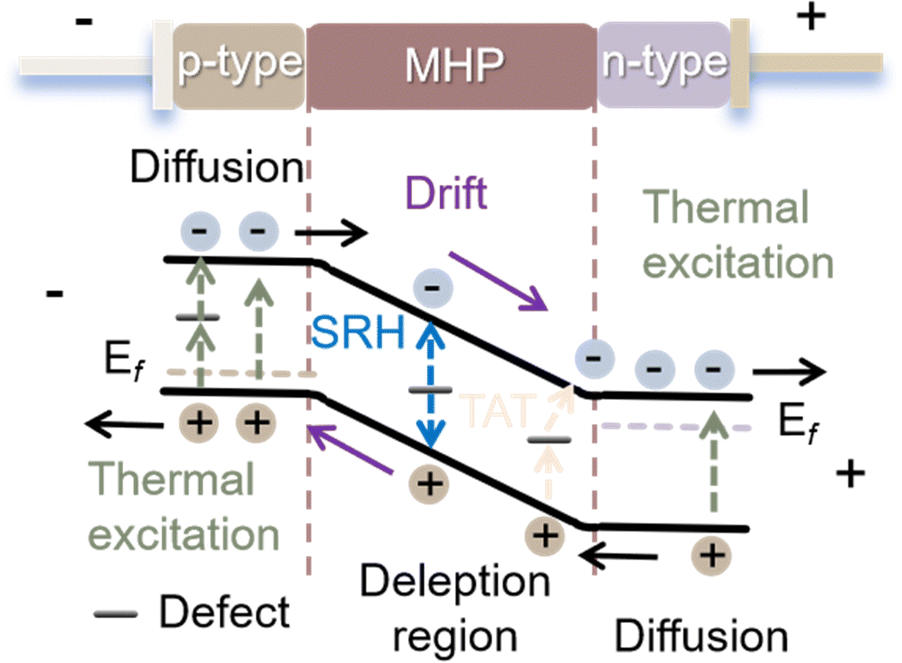 | ||
| Fig. 3 The typical components and generation mechanisms of dark current in MHPPDs. | ||
According to the following equation, Jdiff of a semiconductor-based photodiode is determined by thermodynamics, such as the carrier density and bandgap of the materials used:
The type of contact can influence Jdiff. In the case of a Schottky contact, where the depletion region serves as the barrier layer, Jdiff consists of various components. One of these components is the thermionic-emission current (JT), which can be calculated using the Richardson–Dushman equation based on the thermionic-emission theory. This equation helps determine the contribution of thermionic emission to the overall Jdiff:22

Another significant source of Jd is the generation-recombination current (Jg−r), which arises from both the bulk depletion region and the interface. According to the Shockley–Read–Hall (SRH) model, Jg–r is determined in the bulk layer:23

Aside from charge injection and bulk thermal generation of charge carriers, tunneling and leakage current processes also affect Jd in photodiodes. Photodiodes typically consist of multiple layers, including an absorber and a charge transport layer. Suppose traps are present in the absorber layer, in that case, trap-assisted tunneling can occur between the valence and conduction bands of the absorber materials or between the absorber materials and subsequent transport layers, increasing Jd.
4.2 Advancements in exploring dark current mechanisms in MHPPDs
In the context of MHPPDs, investigating the factors that influence Jd is essential for elucidating its origin. Researchers have identified that one of the primary origins of Jd in MHPPDs is the migration of ions through the bulk of the grains via point defects or extended defects, such as grain boundaries, which are considered material imperfections specific to MHPPDs. A study conducted by Jang et al. compared MHPPDs based on Pb and Sn MHP films. The researchers discovered that vertical grain boundaries in these materials contribute to increased Jd, while horizontal grain boundaries have the opposite effect of reducing Jd.24 This disparity can be attributed to smaller grains in the Sn-based MHPs, resulting in divergent shunt pathways for Jd. (Fig. 4a) Consequently, Yang et al. conducted a study in which they observed a decrease in the Jd of MHP films containing potassium salt additives by reducing the crystal grain size of Sn-based MHPs. This reduction in Jd was attributed to the increased presence of shunting paths.25 Furthermore, the inherently weaker halide-ion migration in the Sn-based material provides an advantage in suppressing Jd. Similarly, Dey et al. conducted an investigation using scan-rate-dependent hysteresis analyses, temperature-dependent impedance spectroscopy measurements, and first-principles calculations on mixed Pb–Sn MHPs.26 Their research revealed the crucial role of Sn vacancies in enhancing the migration barrier of iodide ions, which occurs due to local structural distortions. Yin et al. conducted a study highlighting the significant contribution of surface iodine vacancies to Jd in polycrystalline MHPPDs.27 Their experimental findings revealed that the trap states induced by surface iodine vacancies within the bandgap can create many generation and recombination centers. Consequently, this leads to a decrease in the minority carrier lifetime and an increase in the generation–recombination current density based on the SRH mechanisms under dark conditions (Fig. 4b). Moreover, Moseley et al. underscored the significance of considering the presence of defects in MHP films, which can result in Jd that exhibit time-dependent drifting over seconds, as they can cause measurement challenges such as speed and LDR.28 These defects and trap states can generate a photoconductive gain by extending carrier lifetimes beyond transit times or altering interface energetics, enabling charge injection even under low light intensity in MHPPDs.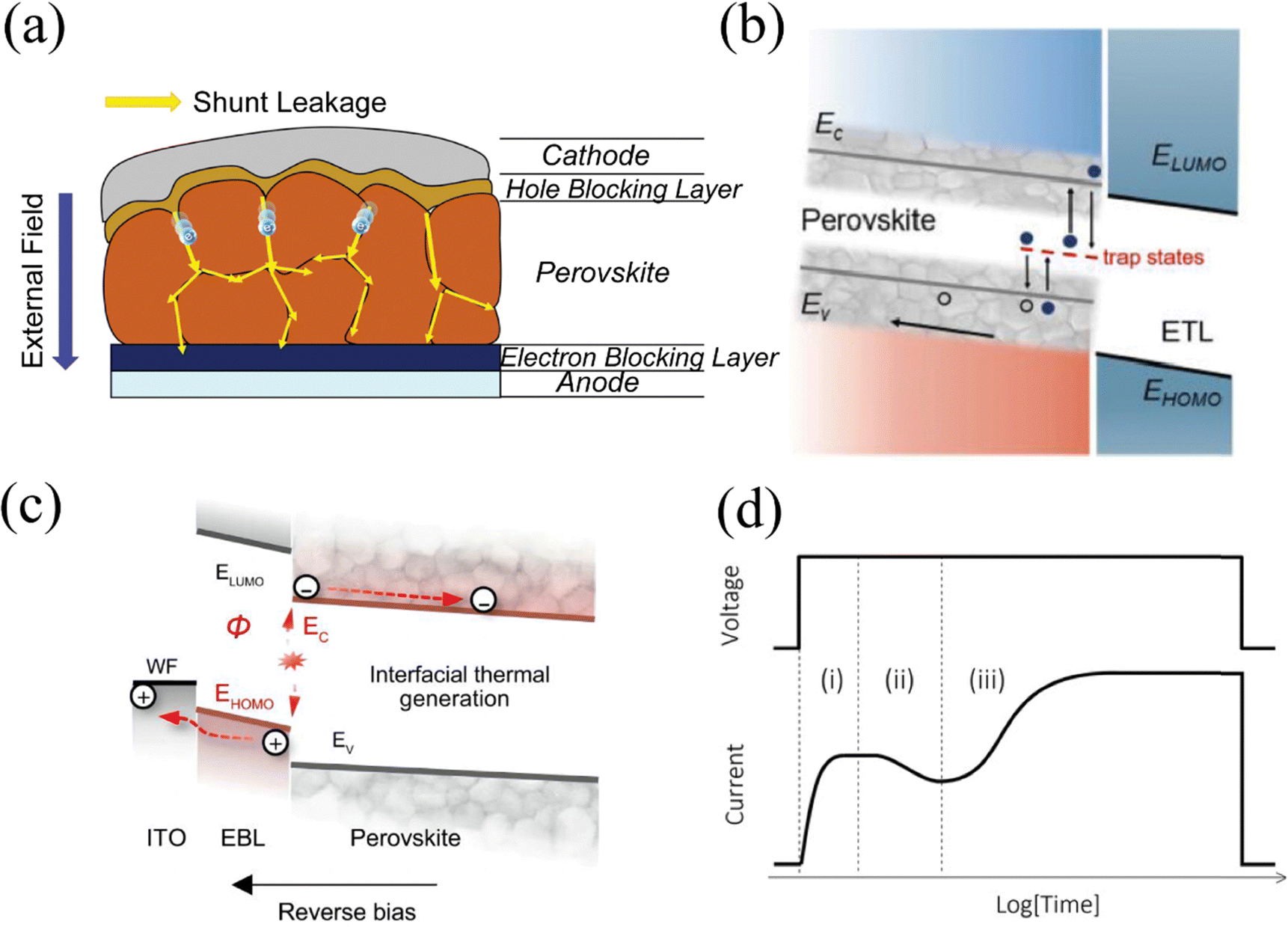 | ||
| Fig. 4 (a) Diagram illustrating the formation of multiple divergent leakage pathways in a Sn-based MHP with a reduced grain size. Reproduced with permission.24 Copyright 2022, Wiley-VCH. (b) Schematic energy level diagram showing the generation–recombination processes enhanced by surface trap states under dark conditions. Reproduced with permission.27 Copyright 2023, Wiley-VCH. (c) Schematic representation of the thermal charge generation mechanism at the EBL-MHP interface. Reproduced with permission.29 Copyright 2021, Nature. (d) Schematic regime of long-term dark reverse bias current response for MHPPDs. Reproduced with permission.30 Copyright 2022, Wiley-VCH. | ||
In addition to the presence of structural and compositional imperfections such as pinholes, trap states, and grain boundary leakage in MHPs, the contact between the MHPs and the charge transport layers (CTLs) or electrodes also significantly influences the experimental Jd of MHPPDs. Sutherland et al. observed that MHPPDs and MHP-based solar cells exhibit differences in their reverse saturation current density.31 Given that  shunt paths are not crucial in limiting Voc (open-circuit voltage) until Rsh (shunt resistance) becomes extremely small. Shunt paths of this magnitude can immensely increase Jd under reverse bias. Thus, it is not always guaranteed that the efforts to optimize solar cell performance will result in sufficiently low Jd for effective photodetection. They further developed the electron contact composites (TiO2/Al2O3/PCBM) for MHPPDs to minimize Jd. Duijnstee et al. discovered that the experimental data must consider an interface injection barrier to fit the TPC measurement.32 They pointed out that the injection barrier and ionization of trapped carriers at the interface contribute to the Jd. Moreover, Ollearo et al. demonstrated that the interfacial energy offset between the electron-blocking layers and the MHPs significantly determines the magnitude of Jd.29 As the offset increases, it can efficiently suppress the thermal charge generation at the interface between electron-blocking layers (EBL) and the MHPs, leading to a significantly lower Jd (Fig. 4c).
4.3 The dark current drift in MHPPDs
The Jd's saturation period under reverse bias conditions commonly known as instabilities in the dark reverse saturation current can lead to measurement inaccuracy in MHPPDs, especially for direct radiation detection. It is worth mentioning that other halide-based radiation detectors under the high reverse bias conditions also face the problem of Jd drift.33 Recent studies have highlighted two leading causes for the Jd drift in MHP films used in direct radiation detection. Firstly, the presence of mobile ions within the bulk and grain boundaries of MHP films can contribute to the drift.34 Secondly, the trapping or accumulating charge carriers at interlayers can also lead to the drift phenomenon. Several techniques and models have been employed to investigate and predict the transient Jd decay characteristics associated with the trapping or accumulating charge carriers at interlayers. Different MHP absorbers and interlayer materials have been studied in this regard.35–37Understanding the ionic conduction in MHPs, in terms of electronic and ionic behaviors, is crucial in comprehending the Jd drift regarding ion migration process. Yang et al. studied MA1−xFAxPbI3, a mixed electronic/ionic material, they discovered that halide (iodine) migration occurs under an electric field in such materials by measuring and modeling the stoichiometric polarization by the mixed conduction.38 Investigating ion mobility in different MHPs is significant due to their known halide ion-conducting properties under dark conditions. García-Batlle et al. conducted a comparative analysis of two compounds, namely MAPbBr3 and MAPbI3, along with different structures, such as single-crystalline and microcrystalline, to study the long-term evolution of Jd.39 To estimate the ion mobility in these systems, they employed ionic time-of-flight measurement techniques and obtained values ranging from 10−7 to 10−6 cm2 V−1 s−1. The results revealed that bromide compounds exhibited lower ion mobility, dependent on the electric field. Conversely, iodide compounds showed higher ion mobility, independent of the electric field. In addition, Almora et al. performed MATLAB code driftfusion simulations to investigate the long-term reverse bias current behavior in MHPPDs.30 (Fig. 4d) Their findings revealed that the steady-state Jd observed under reverse bias is primarily an electronic current rather than an ionic current, even though the presence and concentration of mobile ions play a crucial role. The reduction of Jd drift through screening is influenced by the following factors: the thickness of the MHPs, the applied electric field, the concentration of mobile ions, and the mobile ion mobility. By employing material engineering techniques such as composition and interface engineering in MHPs, it is possible to reduce the screening of Jd drift.
5. Strategies for suppressing dark current toward high performance MHPPDs
Comprehending the components and underlying mechanisms of Jd in photodiodes is crucial for understanding their operational behavior. This knowledge facilitates the development of targeted strategies to mitigate Jd in MHPPDs. For instance, operating these devices at lower temperatures can effectively reduce the intrinsic carrier concentration within the MHP film, which serves to suppress Jdiff. Additionally, employing techniques such as compositional modulation and bulk passivation can enhance the MHP film quality and reduce inherent material defects, thereby diminishing Jg−r. Furthermore, employing interfacial engineering strategies, including the use of insertion layers or passivation techniques, can crucially curb surface or interfacial defects. This, in turn, helps to decrease Jd associated with trap-induced carrier generation and recombination. The application of heterojunctions allows for the integration of MHP with other materials, promoting optimal band alignment, reducing surface defects, and tuning related optical and electrical properties. Such alignment, aided by the built-in potential, acts as a barrier against the flow of majority carriers to decrease Jdiff. Moreover, modifications in device architecture can influence carrier transport mechanisms and promote band bending, which further prevents carrier recombination. In the following section, we delineate comprehensive strategies for mitigating Jd in both the material composition and device structure to boost performance and ensure the reliability of optoelectronic applications, as shown in Fig. 5. | ||
| Fig. 5 Schematic illustration of the components of Jd and the methods for suppressing the Jd of MHPPDs. | ||
5.1 Component modulation
As ionic crystals, MHPs exhibit formation energies for anion/cation vacancies that are largely influenced by Coulomb interactions between the ions and crystal frameworks. By precisely controlling the composition of MHP crystals, it becomes feasible to enhance bonding energy, alleviate stress, optimize morphology and crystallinity, and significantly decrease Jd.For instance, as shown in Fig. 6(a)–(c), Yun et al. investigated the engineering of A-site monovalent cations in wide-bandgap MHPs for high-performance blue photodetection.40 Their findings revealed that introducing FA in MA increased the heat of formation, leading to modulated nucleation and grain growth behavior. Furthermore, the incorporation of optimal Cs (5%) helped mitigate strain and decrease trap states in the MHP thin film, resulting in a more compact and better-arranged crystal lattice. These improvements enabled the fabrication of N–I–P devices with a decent D* of 5.08 × 10¹² Jones, and demonstrated the feasibility of individual 7 × 7 devices for real image sensing under 450 nm blue light illumination. Additionally, Liu et al. explored the modulation of A-site monovalent cations and X-site halide anions in MHPPDs for direct X-ray detection.41 They observed that smaller cations (MA+ and Cs+) and anions (Br−) resulted in the release of lattice stress and improved morphology, as evidenced in Fig. 6d. The optimized composition of FA0.85MA0.1Cs0.05PbI2.55Br0.45 exhibited superior properties, including an ultra-low trap density of (4.6 ± 2.4) × 109 cm−3, a long carrier lifetime of 6.4 μs, and a diffusion length of 68.9 μm. This composition achieved an extremely low Jd of −1.44 μA cm−2 at −75 V bias, and a low detection limit of 42 nGyair s−1. Furlan et al. demonstrated the tunable halide composition in organic cation-based MHPs.42 By adding Br to MAPbI3-based MHPs, they not only adjusted the bandgap through lattice contraction but also reduced non-radiative recombination losses in MHP layers by tuning the crystallite size, as shown in Fig. 6f. They established a correlation between the reduced Jd (1.3 × 10⁻⁹ A cm−2 at −0.5 V), Voc enhancements (Fig. 6e), and achieved high-performance MHPPDs (D* of 8.7 × 10¹² Jones) within the range of 350–850 nm. Although inorganic MHPs (CsPbX3) are suitable for high-performance and stable photodetection applications, they also exhibit thermodynamic instability at room temperature and spontaneously transform into a photo-inactive phase under ambient conditions due to the small tolerance factor. Li et al. demonstrated high-performance MHPPDs with an ultra-low Jd (6.4 × 10⁻⁵ mA cm−2) (Fig. 6i) and a high speed of 558 ns by utilizing the organic cation DMA (DMA+ = dimethylammonium, (CH3)2NH2+) to enhance the room-temperature phase stability of Cs-based MHP thin films.43 The blue shift of the diffraction peak position observed in Fig. 6g was attributed to the introduction of DMA+, which has a larger ionic size than Cs+. In addition, this finding was supported by the photoluminescence spectra (PL) of the Cs+ and DMA+-based MHP films.
 | ||
| Fig. 6 (a) Jd, and photocurrent density, and on/off ratio with the different FA/MA ratios. (b) Strain components of control and Cs-incorporating MHP films. (c) Trap density and mobility of control and Cs-incorporating MHP films obtained from the electron/hole-only configuration. Reproduced with permission.40 Copyright 2022, Wiley-VCH. (d) Schematic illustration of the lattice stress release of the 3-cation mixed-halide FAMACs MHPs. Reproduced with permission.41 Copyright 2020, Wiley-VCH. (e) The relationship between Jd and Voc with various halide Br and I ratios. (f) Surface morphology of MAPb(I1−xBrx)3 MHP thin films obtained by scanning electron microscopy. Reproduced with permission.42 Copyright 2022, Wiley-VCH. (g) and (h) XRD patterns and PL spectra of the CsxDMA1−xPbI3 films. (i) J–V curves of MHPPDs in the dark based on the CsxDMA1−xPbI3 films. Reproduced with permission.43 Copyright 2020, Elsevier. | ||
In addition to the effective modulation of A-site and X-site components to reduce Jd and improve device performance, researchers have also been exploring B-site regulation. For instance, hybrid Pb–Sn MHP-based MHPPDs have been investigated to achieve a broad spectral response ranging from 300 nm to 1000 nm, while also reducing Jd compared to Pb-based devices, thanks to the reduced trap density.44 Furthermore, researchers have conducted halide composition modulation to develop nontoxic bismuth MHPs.45 All of these demonstrations highlight the significant potential of component modulation in MHPs for effectively suppressing Jd and enhancing device performance. An update on the progress in the reported component modulation of the MHPPDs is provided in Table 1.
| Strategy | Device structure | Dark current (density) (Id or Jd) | D* (Jones) | Speed [rise time (tr)/fall (decay) time (tf)] | LDR (dB) | Ref. |
|---|---|---|---|---|---|---|
| a Noise signal: the noise signal in photodetection is recorded by utilizing a fast Fourier transform signal analyzer combined with a preamplifier to capture the noise current at various frequencies. b Detection limit: the detection limit in X-ray detection is defined as the equivalent dose rate to produce a photocurrent greater than three times the noise current (dark current). c TPC extracted: speed here can be defined as the time at which the photocurrent decays from the peak to the original 1/e extracted from the transient photocurrent curves. | ||||||
| Reduce bulk defects (rubidium incorporated into FAPbI3) | ITO/PEDOT:PSS/MHP/C60/BCP/Cu | 10−10 A cm−2 (0 V, about 100 times reduced) | 1.7 × 10¹² | 300/— ns | 125 | 46 |
| Alleviate stress and reduce bulk defects (Cs incorporated into FAPbI3) | ITO/MeO-2PACz/MHP/C60/BCP/Ag | 3.3 × 10⁻⁹ A cm−2 (−0.5 V) | 6.1 × 10¹¹ | 1.2/1.2 μs | 135 | 47 |
| Optimize morphology and crystallinity (Cs and Br optimization in FAPbI3) | ITO/MoO3/TaTm/MHP/C60/CN-T2T:C60/Ag | 8.627 × 10⁻¹⁰ A cm−2 (0 V) | 1.747 × 10¹³ (530 nm) | 629/616 ns | 127 | 48 |
| Alleviate stress and reduce bulk defects (Cs, MA, FA optimization in APbBr2Cl) | ITO/SnO2/MHP/PMMA/Spiro-OMeTAD/Au | 3.04 × 10⁻⁸ A cm−2 (0 V) | 5.57 × 10¹² | 585/531 μs | — | 40 |
| Optimize morphology and crystallinity (Br, Cl, I optimization in MAPbX3) | ITO/SnO2/MHP/Spiro-OMeTAD/Au | 2.7 × 10⁻⁷ A cm−2 (0 V) | 8.65 × 10¹¹ | 2.35/2.87 ms | — | 49 |
| Optimize morphology and crystallinity (Br, I optimization in Cs3Bi2I9−xBrx) | ITO/PEDOT:PSS/MHP/C60/BCP/Ag | 3.5 × 10⁻⁹ A cm−2 (0 V) | 4.6 × 10¹¹ (410 nm) | 40.7/27.1 ms | — | 45 |
| Reduce bulk defects (FA incorporated into MAPbI3) | ITO/PTAA/MHP/C60/BCP/Cu | 0.02 pA Hz−1/2 (noise signal)a (0 V) | 27.7 nGyair s−1 (detection limit)b | 86/500 μs | — | 50 |
| Reduce bulk defects and increase film thickness (Cs, DMA optimization in CsxDMA1−xPbI3) | ITO/PTAA/PMMA/MHP/PCBM/Bphen/Cu | 6.4 × 10⁻⁵ mA cm−2 (−0.2 V, about 103 times reduced) | Over 1.0 × 10¹³ | 558 ns (TPC extracted)c | — | 43 |
| Optimize morphology, reduce bulk defects (Br, Cl optimization in CsPbBrxCl3−x) | ITO/MHP/Au | 10−8 A cm−2 (0 V) | 1012 | 75/70 μs | 137 | 51 |
| Alleviate stress and reduce bulk defects (Cs, MA, FA and Br, I optimization in MHPs) | Au/BCP/C60/MHP/SpiroTTB/Au | −1.44 μA cm−2 (−75 V) | 42 nGyair s−1 (detection limit)b | 2.3/57.2 μs | — | 41 |
| Optimize morphology (FA, and Sn optimization in MHPs) | ITO/PEDOT:PSS/MHP/C60/BCP/Ag | 5.2 × 10⁻⁸ A cm−2 (−0.2 V) | 1012 | 6.9/9.1 μs | 167 | 52 |
| Optimize morphology and reduce bulk defects (Br, I optimization in MAPbBr3−xIx) | ITO/MeO-2PACz/MHP/PCBM/BCP/Cu | 1.3 × 10⁻⁹ A cm−2 (−0.5 V, about 20 times reduced) | 8.7 × 10¹² | 0.58/0.17 μs | 133 | 42 |
5.2 Dimensional engineering
Numerous studies have shown that effective dimensional regulation of MHPPDs using hydrophobic organic cations can reduce the dimension of MHPs and transition them from 3D to quasi-2D structures. This not only helps suppress defects, thanks to the high defect formation energies of quasi-2D MHPs, but also significantly improves their stability. Thus, efforts have focused on creating a quasi-2D MHP layer at the interface, forming a 2D/3D MHP structure.27,53–55 This approach leads to fewer trap states at the MHP and electrode interface, consequently improving device performance. However, it is important to note that excessive presence of 2D MHPs at the interface, as well as disordered phase distribution, can impede charge transport due to the insulating effect of the bulkier, long-chain organic spacer cations (as illustrated in Fig. 7a). Recent efforts have therefore aimed at creating uniformly distributed, compact 2D–3D gradient MHPs with an ordered phase distribution along the thin film's longitudinal direction, as this offers enhanced optoelectronic properties, stability, and ideal MHPPD characteristics. For instance, Miao et al. employed the hot-casting method to control the phase distribution of quasi-2D MHP thin films.56 By comparing the top and bottom PL spectra of different MHP thin films (as shown in Fig. 7b), they studied the effects of substrate temperature on surface morphology and internal phase distribution. The resulting device showed an extremely low Jd (2.3 × 10⁻¹¹ A cm−2), large D* at 455 nm (1.22 × 10¹⁴ Jones), ultra-fast speed (5.5/4.7 μs), and remarkable stability. Additionally, Peng et al. reported an ion-exchange strategy to prepare 2D-3D thick MHP films with uniform morphology, vertically aligned monolithic crystal phases, and reproducibility (as shown in Fig. 7c).57 By performing an ion exchange between Br− and I− halide anions, they achieved a slow crystallization process resulting in a gradient phase distribution of 2D–3D MHP thick films. In situ PL spectra monitoring helped unveil the effect of halide anions (Br− and I−) on crystal formation in these thick MHP films (Fig. 7d). The resulting 2D–3D MHP thick film-based devices exhibited extremely low Jd (0.8 nA cm−2), an ultra-fast speed of 640 ns, and a detection limit of 4.2 nGyair s−1. Furthermore, they demonstrated a prototype 1024-pixel detector array for X-ray imaging. The strategies and the corresponding device structures and performance parameters are summarized in Table 2. These advancements in engineering the dimensional and phase distribution of MHPs hold great promise for achieving high-performance and stable MHPPDs. | ||
| Fig. 7 (a) Schematic diagram of the internal phase arrangement process and the corresponding charge transportation in MHP thin films. (b) The top and bottom PL spectra of different phase arrangement films. Reproduced with permission.56 Copyright 2023, Elsevier. (c) Schematic illustration of the self-assembled 2D–3D MHPs obtained by an ion-exchange-induced crystallization method. (d) PL spectra monitoring of different 2D–3D MHP combinations.57 Reproduced with permission. Copyright 2022, Elsevier. | ||
| Strategy | Device structure | Dark current (density) (Id or Jd) | D* (Jones) | Speed [rise time (tr)/fall (decay) time (tf)] | LDR (dB) | Ref. |
|---|---|---|---|---|---|---|
| a TPC extracted: speed here can be defined as the time at which the photocurrent decays from the peak to the original 1/e extracted from the transient photocurrent curves. b Detection limit: the detection limit in X-ray detection is defined as the equivalent dose rate to produce a photocurrent greater than three times the noise current (dark current). c Noise signal: the noise signal in photodetection is recorded by utilizing a fast Fourier transform signal analyzer combined with a preamplifier to capture the noise current at various frequencies. d Drifting: drifting means the dark current drift period D. | ||||||
| Regulate band alignment (quasi 2D (BDA0.7(BA2)0.3)(EA)2Pb3Br10 MHPs) | ITO/bl-TiO2/mp-TiO2/MHPs/PTAA/Au | 2.65 × 10⁻¹² A (0 V) | 2.5 × 10¹⁵ | 270/920 μs | — | 58 |
| Regulate band alignment (2D/3D (BzA)2MAn−2PbnI3n+1/MAPbI3) | ITO/bl-TiO2/mp-TiO2/MHPs/PTAA/Au | 8.32 × 10⁻¹⁰ A cm−2 (0 V, about 1.79 times reduced) | 1.21 × 10¹³ | 53/38 μs | — | 59 |
| Optimize morphology and reduce bulk defects (quasi 2D (BA)2MA3Pb4I13) | ITO/PEDOT:PSS/MHP/PCBM/BCP/Ag | 2.3 × 10⁻¹¹ A cm−2 (0 V) | 1.22 × 10¹⁴ | 5.5/4.7 μs | 173.4 | 56 |
| Optimize morphology and crystallinity, reduce bulk defects (quasi 2D PEA2MA4Pb5I16) | ITO/PEDOT:PSS/MHP/PCBM/BCP/Ag | 0.36 pA Hz−1/2 (noise signal)c (0 V) | 1.4 × 10¹² | 64/162 μs | 120 | 60 |
| Regulate band alignment (quasi 2D (BA)2MA4Pb5I16) | ITO/PTAA/MHP/C60/BCP/Ag | 5 × 10⁻⁹ mA cm−2 (0 V) | 7 × 10¹² (600 nm) | 1.48/1.58 μs | >200 | 61 |
| Regulate band alignment (quasi 2D (PEA)2(MA)59Pb60I181) | FTO/TiO2/MHP/Spiro-OMeTAD/Au | 1.76 × 10⁻⁷ A cm−2 (0 V) | 2.20 × 10¹² (750 nm) | 1.59/0.02 s | 41 | 62 |
| Reduce surface defects and increase crystallinity (2D/3D/2D PEAI/Cs0.05MA0.45FA0.5Pb0.5Sn0.5I3/PEAI) | ITO/PTAA/PEAI/MHP/PEAI/C60/BCP/Cu | 1.25 × 10⁻³ mA cm−2 (−0.1 V) | 2.07 × 10¹¹ (910 nm) | 35 ns TPC extracteda | — | 54 |
| Alleviate stress and reduce bulk and interface defects (2D/3D (PTABr and PEABr)/tri-cation MHPs) | ITO/PEDOT:PSS/MHP/PCBM/Ag | — | 1012 (730 nm) | 40 μs TPC extracteda | — | 53 |
| Optimize morphology and crystallinity (quasi 2D (BA)2MAn−2PbnI3n+1) | ITO/PTAA/MHP/C60/BCP/Au | 10−5 mA cm−2 (3 kV cm−1) | — | — | — | 63 |
| Optimize morphology and crystallinity (2D-3D (BA2PbBr4)0.5FAPbI3) | ITO/NiOx/PEIE/MHP/C70/BCP/Au | 0.8 nA cm−2 | 4.2 nGy air s−1 (detection limit)b | 640 ns/— | — | 57 |
| Regulate band alignment, optimize morphology and crystallinity and reduce surface defects (2D/3D PEAI/MAPbI3) | ITO/SnO2/MHP/PTAA/Au | ∼3.1 × 10⁻¹⁴ A Hz−1/2 (noise signal)c (0 V, about 1.8 times reduced) | 2.57 × 10¹² (740 nm) | 1.7/9.8 μs | 161 | 55 |
| Optimize morphology and crystallinity (2D–3D (PA2PbI4)x(FA0.83Cs0.17PbI3)1−x) | ITO/PTAA/PEIE/MHP/C60/BCP/Cu | 7 fA Hz−1/2 (noise signal)c (−0.5 V) | 3.7 × 10¹³ | <80 ns | 182 | 64 |
| Optimize morphology and reduce bulk and surface defects (quasi 2D PEA2MA8Pb9I28) | ITO/MHP/Au | 1.8 × 10⁻² pA cm−1 s−1 V−1 (drifting)d | 69 nGyair s−1 (detection limit)b | — | — | 65 |
| Reduce surface defects (2D/3D PEA2PbBr4/MAPbI3) | ITO/MHP/Au | 2.6 × 10⁻¹⁰ A cm−2 (0.5 V mm−1) | 10.17 nGyair s−1 (detection limit)b | 228/197 μs | — | 66 |
| Reduce surface defects (2D/3D BAI/MAPbI3) | ITO/NiOx/MHP/PCBM/Bphen/Ag | 3.78 × 10⁻¹⁰ A cm−2 (−0.1 V) | 1.46 × 10¹² | 1.03/3.20 μs | — | 27 |
| Regulate band alignment (quasi 2D (PEA)2MA3Pb4I13) | ITO/MHP/PCBM/Ag | 0.4 nA (0 V) | 3.38 × 10¹² (570 nm) | 20.8/20.6 μs | 99.6 | 67 |
5.3 Additive engineering and the modulation of crystallization methods
Being an ionic crystal, the occurrence of anion/cation vacancies within the bulk and at the interface of MHPs is inevitable during the thin film formation process. To address this, a passivation technique involving the addition of additives in the bulk and at the interface of MHPs has been developed. This technique creates coordinating bonding, eliminates vacancies, and fills interstitial spaces, ultimately leading to a reduction in Jd of the MHPPDs. We have summarized the progress in MHPPDs achieved through the application of relevant additive engineering for both the bulk and interface of MHPs in Table 3.| Strategy | Device structure | Dark current (density) (Id or Jd) | D* (Jones) | Speed [rise time (tr)/fall (decay) time (tf)] | LDR (dB) | Ref. |
|---|---|---|---|---|---|---|
| a Noise signal: the noise signal in photodetection is recorded by utilizing a fast Fourier transform signal analyzer combined with a preamplifier to capture the noise current at various frequencies. b TPC extracted: speed here can be defined as the time at which the photocurrent decays from the peak to the original 1/e extracted from the transient photocurrent curves. c Detection limit: the detection limit in X-ray detection is defined as the equivalent dose rate to produce a photocurrent greater than three times the noise current (dark current). | ||||||
| Optimize morphology and crystallinity (Mn doped into Cs2AgBiBr6) | ITO/SnO2/MHP/Ag | — | 3.46 × 10¹⁰ (405 nm) | 3.4/2.0 μs | 130.5 | 68 |
| Optimize morphology, crystallinity and reduce bulk defects (Cs doped into FA0.75MA0.25PbI3) | ITO/PEDOT:PSS/MHP/PCBM/BCP/Al | — | 1.15 × 10¹² | 1.5/21 μs | — | 69 |
| Reduce bulk defects (Cl doped into MAPbI3) | ITO/PEDOT:PSS/MHP/C60/BCP/Cu | 8.4 × 10⁻⁸ A cm−2 (−0.1 V, about 11 times reduced) | 2.71 × 10¹² | — | 104 | 70 |
| Optimize morphology (spray-coated CsPbBr3 quantum dots) | FTO/TiO2/MHP/Spiro-OMeTAD/Au | 4 × 10⁻⁴ mA (0 V, about 20 times reduced) | 1 × 10¹⁴ (365 nm) | — | 90 | 71 |
| Optimize morphology and crystallinity, and reduce bulk and surface defects (room-temperature crystallization for Sn–Pb MHP) | Electrode/MoO3/PEDOT:PSS/MHP/PCBM/ZrAcac/Electrode | (2.8 ± 0.81) × 10−7 A cm−2 (0 V) | 1011 | 90 ns/2.27 μs | 100 | 72 |
| Optimize morphology and crystallinity (thick FAPbI3 junctions) | ITO/Poly-TPD/CsI/MHP/C70/BCP/Cu | — | — | 60 ns (TPC extracted)b | — | 73 |
| Reduce bulk and surface defects (MAPbI3 and MAPbBr3 thin-single-crystals) | ITO/PTAA/MHP/C60/BCP/Cu | 1–2 fA Hz−1/2 (noise signal)a | 1.5 × 10¹³ (532 nm) | 4 ns (TPC extracted)b | 256 | 74 |
| Optimize morphology and crystallinity, and reduce bulk defects (AgI additive in CsPbIBr2) | FTO/compact TiO2/MHP/Spiro-OMeTAD/Au | 9.71 × 10⁻⁶ A cm−2 (0 V, about 4.5 times reduced) | 2.46 × 10¹¹ | 22.4/25.7 μs | — | 75 |
| Regulate band alignment and reduce surface defects (P3HT additive in CsSnBr3) | ITO/ZnO/MHP/CuSCN/Ag | 10−10 A | 1.40 × 10¹⁴ (532 nm) | 195.2/165.8 ms | 115 | 76 |
| Reduce surface defects (thioacetamide (TAA) as an interface material on CsPbBr3) | ITO/SnO2/MHP/TAA/Spiro-OMeTAD/Ag | 3.13 nA cm−2 (0 V) | 8.39 × 10¹² | 1.05/5.04 μs | 118 | 77 |
| Reduce surface defects and regulate band alignment (rubrene as an interface material on CsPbBr3) | ITO/ZnO/MHP/rubrene/Au | 1.04 × 10⁻¹⁰ A | 2.61 × 10¹³ | 79.4/207.6 μs | — | 78 |
| Reduce crystalline temperature and optimize morphology (ionic liquid 1-butyl-2,3-dimethylimidazolium chloride additive in Cs2AgBiBr6) | FTO/SnO2/MHP/carbon | 5 nA | 1.87 × 10¹² | 0.24/0.29 ms | 100 | 79 |
| Reduce bulk and surface defects (3-(1-pyridinio)-1-propanesulfonate (PPS) for the buried layer and the additive for MHP) | ITO/SnO2/PPS/MHP:PPS/Ag | 6.05 × 10⁻¹¹ A (about 2 times reduced) | 1.51 × 10¹³ | 0.74/0.09 s | — | 80 |
| Regulate band alignment and optimize crystallinity (NH4Cl additive and DMSO solvent for (PEA)2MA3Pb4I13) | ITO/PEDOT:PSS/MHP/PCBM/Bphen/Al | 1.7 × 10⁻⁴ mA cm−2 (about 2 times reduced) | 6 × 10¹¹ (600 nm) | 5.8/4.6 ms | 126 | 81 |
| Regulate band alignment and reduce surface and bulk defects (carbohydrazide (CBH) as an additive for (PEA)2MA3Pb4I13) | ITO/MHP/PCBM/Ag | — | 1.31 × 10¹² (570 nm) | 0.532/0.521 ms | — | 82 |
| Reduce surface defects (4-amino-2,3,5,6-tetrafluorobenzoic acid (ATFBA) as an additive for Cs0.15FA0.85Pb0.5Sn0.5I3) | ITO/PTAA/MHP/C60/BCP/Cu | 1.2 × 10⁻⁵ mA cm−2 (−0.1 V, about 10 times reduced) | 5.34 × 10¹² (850 nm) | 39.68 ns (TPC extracted)b | 224 | 83 |
| Optimize morphology and crystallinity (3,3,4,4-benzophenonetetracarboxylic dianhydride (BPTCD) as an additive for MAPbI3) | ITO/PEDOT:PSS/MHP/PCBM/Ag | 9.98 × 10⁻⁸ A (−0.5 V, about 29 times reduced) | 4.55 × 10¹¹ (685 nm) | 850/800 ms | — | 84 |
| Optimize crystallinity and reduce surface defects (urea as an additive for MAPbI3) | ITO/NiOx/MHP/PCBM/BCP/Ag | 3.48 × 10⁻⁸ A cm−2 (−0.1 V, about 3 times reduced) | 7.28 × 10¹² | 5/18 μs | — | 85 |
| Reduce surface and bulk defects (trimethylolpropane triacrylate (TMTA) crosslinked MAPbI3) | ITO/MHP/Au | 2.35 × 10⁻¹⁴ A Hz−1/2 (noise signal)a 8.8 fA cm−1 s−1 V−1 (drifting)d | 67 nGy s−1 (detection limit)c | — | — | 86 |
| Optimize morphology and crystallinity (1-butyl-3-methylimidazolium bromide (BMIMBr) as an additive for CsPbBr3) | ITO/SnO2/MHP/Carbon | 2.51 × 10⁻¹⁰ A (0 V) | 4.31 × 10¹² | 0.06/0.26 ms | 140 | 87 |
| Regulate band alignment and optimize crystallinity (NH4SCN and NH4Cl as the dual additives for 2D/3D TEA-based MHP) | ITO/NiOx/MHP/PCBM/ZnO/Ag | 2.43 nA cm−2 (0 V, about 28 times reduced) | 2.46 × 10¹² (610 nm) | 42.8/135.2 ns | 111.4 | 88 |
| Reduce bulk and surface defects (ascorbic acid (AA) as an antioxidant additive for MA0.5FA0.5Pb0.5Sn0.5I3) | ITO/PEDOT:PSS/MHP/PC61BM/bis-C60/Ag | 1.5 pA Hz−1/2 (noise signal)a | 1012 (800–1000 nm) | 7.4 μs | 1010 (photon number) | 89 |
| Reduce surface defects, optimize morphology and crystallinity (two-step spin-coating method for MAPbI3) | ITO/PEDOT:PSS/MHP/PC61BM/BCP/Au | 5.55 × 10⁻⁴ mA cm−2 (−1.5 V, about 3 times reduced) | 5 × 10¹¹ (532 nm) | 2.6/72.8 μs | 106 | 90 |
| Reduce surface defects (thiophene-2-carbohydrazide (TAH), an antioxidant additive for FA0.7MA0.3Pb0.5Sn0.5I3) | ITO/PEDOT:PSS/MHP/PC61BM/C60/BCP/Ag | 1.5 × 10⁻⁸ mA cm−2 (−0.07 V) | 1.8 × 10¹² (840 nm) 2.5 × 10¹² (940 nm) | 94/97 ns | — | 91 |
| Reduce bulk and surface defects (an urea additive for MAPbI3) | ITO/NiOx/MHP/PCBM/BCP/Ag | 1.82 × 10⁻¹¹ mA cm−2 | 1.42 × 10¹⁴ | — | 162 | 92 |
| Optimize crystallinity and reduce surface defects (tetrafluoroborate and hexafluorophosphate additives for FAPbI3) | ITO/PTAA/PEIE/MHP/C70/BCP/Cu | 7.7 × 10⁻¹⁰ A cm−2 (−0.2 V) | 1012 | 188/630 ns | 132 | 93 |
| Optimize morphology and crystallinity, and reduce bulk and surface defects (fluorinated aminobenzoic acid isomers [3-amino-2,6-difluorobenzoic acid (13-FABA) and 4-amino-3,5-difluorobenzoic acid (14-FABA)] as additives for CsPbIBr2) | FTO/SnO2/MHP/P3HT/Ag | 2.2 × 10⁻¹⁰ mA cm−2 (0 V, 104 times reduced) | 1.69 × 10¹³ | 23.5/21.2 ms | 41.93 | 94 |
| Reduce bulk and surface defects (1-butyl-2,3-dimethylimidazolium chloride (BMIMCl) and PMMA as additives for CsSnI3) | ITO/SnO2/MHP/Carbon | 2 × 10⁻¹¹ A | 1.18 × 10¹² | 0.23/0.19 ms | 180 | 95 |
| Optimize morphology and crystallinity (AgI as an additive for CsSnI3) | ITO/PTAA/PEIE/MHP/PC60BM/C70/BCP/Cu | — | 3.5 nGy s−1 (detection limit)c | 280/450 ns | — | 96 |
| Optimize morphology and reduce surface defects (excess PMMA as an additive for MAPbI3) | ITO/PEDOT:PSS/MHP/PC61BM/Au | 3.46 × 10⁻⁴ mA (−1 V, about 2 times reduced) | 3.38 × 10¹² (532 nm) | 5.90/6.75 μs | 80 | 97 |
| Optimize morphology and reduce bulk and surface defects (poly(ethylene glycol) (PEG) additives for CsPbI2Br) | ITO/SnO2/MHP/PTAA/MoO3/Ag | 4.40 × 10⁻⁸ A cm−2 (about 778 times reduced) (−0.1 V) | 1.9 × 10¹¹ (532 nm) | 0.03 ms | 119 | 98 |
| Optimize morphology and crystallinity, reduce surface defects (PMMA/sodium borate salt (Borax) as interface materials for Cs0.05FA0.6MA0.35Pb(Br0.6Cl0.4)3) | ITO/SnO2/MHP/Spiro-OMeTAD/Ag | 1.53 × 10⁻⁹ A cm−2 (0 V, about 8 times reduced) | 7.74 × 10¹² (450 nm) | 0.155/0.155 s | — | 99 |
| Optimize morphology and crystallinity, reduce surface defects (tin thiocyanate additive for FA0.85Cs0.15Sn0.5Pb0.5I3) | ITO/PEDOT:PSS/MHP/MHP/PCBM/ZrAcac/Ag | 9.85 × 10⁻⁸ A cm−2 (−0.4 V, about 60 times reduced) | 8.48 × 10¹² (910 nm) | 67.5 ns/0.72 μs | 213 | 100 |
| Optimize morphology and reduce surface defects (MAPbI3/PMMA) | ITO/NiOx/MHP/PCBM/ZnO/BCP/Al | 5.7 × 10⁻⁷ mA (0 V, about 2 times reduced) | 1.07 × 10¹² | 50/17 μs | 127 | 101 |
| Reduce surface defects (3,4,5-tris (n-dodecyloxy) benzoylamide with an azobenzene moiety (TBA-Azo) additives for Sn–Pb MHP) | ITO/PTAA/MHP/TBA-Azo/C60/BCP/Cu | 9.61 × 10⁻⁵ mA cm−2 (−0.1 V, about 100 times reduced) | 2.21 × 10¹¹ (758 nm) | 42.9 ns (TPC extracted)b | 185 | 102 |
| Optimize morphology, reduce surface defects (PMMA as a double-sided passivation layer) | ITO/NiOx/PMMA/MHP/PMMA/PCBM/ZnO/BCP/Al | 4.0 × 10⁻⁷ mA cm−2 (0 V, about 2 times reduced) | 1.28 × 10¹² | 57/18 μs | 139 | 103 |
For instance, Wang et al. devised a moisture-triggered additive, poly(vinyl alcohol) (PVA), to passivate surface defects in FAPbI3.104 Their results demonstrate that the PVA organic framework fills the grain boundaries of FAPbI3, thereby stabilizing the favorable black phase of FAPbI3 and guarding against moisture intrusion through strong interactions with water molecules. The PVA-passivated FAPbI3 films also exhibit self-healing capabilities upon bending, activated by water molecules (Fig. 8a). Ionic liquids serve as promising candidates for bulk defect passivation in MHPs due to their diverse controllable sources of anions and cations. Gao et al. showcased the effectiveness of 1-butyl-2,3-dimethylimidazolium chloride (BMIMCl) in passivating defects within CsSnI3 NW-based films.95 Their study revealed that BMIMCl exerts a potent passivating effect on Sn-related defects through the large π-bonds in N–C![[double bond, length as m-dash]](https://www.rsc.org/images/entities/char_e001.gif) N, enhancing electron density around Sn2+ in CsSnI3 and shielding it from oxidation to Sn4+. By combining polymethyl methacrylate (PMMA) for bulk defect passivation in CsSnI3 NW-based films, the CsSnI3-based MHPPDs demonstrated reduced Jd and highly stable behavior (Fig. 8b). Thiocyanate salts are recognized as effective additives for controlling the crystallization process and delaying oxidation through strong interactions with metal cations. Liu and colleagues investigated the impact of multifunctional tin thiocyanate (Sn(SCN)2) additives on Sn–Pb MHPs.100 Their addition of the additive to the Sn–Pb MHP precursor led to a preferred double-sided surface distribution within the MHP film, effectively reducing Sn oxidation levels (Fig. 8c). Subsequently, they achieved a high D* (8.48 × 10¹² Jones at 910 nm) and outstanding stability (lifetime of 2300 h) in NIR MHPPDs. Effective additives in the bulk of quasi-2D MHPs can regulate the 3D MHP phase within quasi-2D MHP films. Di et al. introduced carbohydrazide (CBH) additives into quasi-2D (PEA)2MA3Pb4I13 precursors, resulting in significantly improved crystallinity and alignment of the 3D phase.82 This enhancement was evident in sharper XRD diffraction peaks and a higher ratio of the 3D MHP phase in quasi-2D MHP films, impacting their absorption characteristics (Fig. 8d).
N, enhancing electron density around Sn2+ in CsSnI3 and shielding it from oxidation to Sn4+. By combining polymethyl methacrylate (PMMA) for bulk defect passivation in CsSnI3 NW-based films, the CsSnI3-based MHPPDs demonstrated reduced Jd and highly stable behavior (Fig. 8b). Thiocyanate salts are recognized as effective additives for controlling the crystallization process and delaying oxidation through strong interactions with metal cations. Liu and colleagues investigated the impact of multifunctional tin thiocyanate (Sn(SCN)2) additives on Sn–Pb MHPs.100 Their addition of the additive to the Sn–Pb MHP precursor led to a preferred double-sided surface distribution within the MHP film, effectively reducing Sn oxidation levels (Fig. 8c). Subsequently, they achieved a high D* (8.48 × 10¹² Jones at 910 nm) and outstanding stability (lifetime of 2300 h) in NIR MHPPDs. Effective additives in the bulk of quasi-2D MHPs can regulate the 3D MHP phase within quasi-2D MHP films. Di et al. introduced carbohydrazide (CBH) additives into quasi-2D (PEA)2MA3Pb4I13 precursors, resulting in significantly improved crystallinity and alignment of the 3D phase.82 This enhancement was evident in sharper XRD diffraction peaks and a higher ratio of the 3D MHP phase in quasi-2D MHP films, impacting their absorption characteristics (Fig. 8d).
 | ||
| Fig. 8 (a) The mechanism of protection and self-healing process by PVA in FAPbI3 films. Reproduced with permission.104 Copyright 2021, Wiley-VCH. (b) MHPPD based on the CsSnI3 with BMIMCl additive and photo/dark current. Reproduced with permission.95 Copyright 2022, Nature. (c) Sn 3d XPS spectra of the pure Sn–Pb and Sn(SCN)2 Sn–Pb films. Reproduced with permission.100 Copyright 2023, ACS. (d) XRD patterns and UV-vis absorption spectra of the control and with CBH quasi-2D MHP films. Reproduced with permission.82 Copyright 2023, Wiley-VCH. | ||
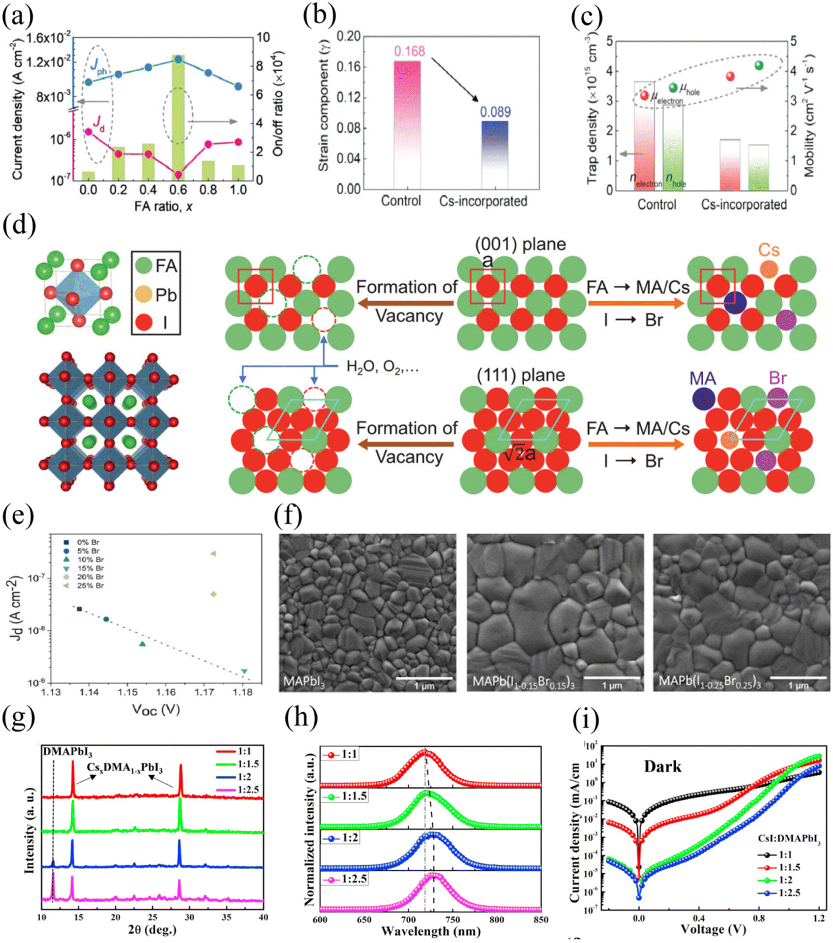
In addition to incorporating additives in the bulk and at the interface of MHPs to passivate defects and regulate phase distribution, researchers have explored modifications to fabrication and crystallization methods to achieve the same objectives. For instance, Bao and colleagues synthesized thin single crystals of MHPs using space confinement methods to significantly reduce bulk defect density and eliminate grain boundaries in polycrystalline MHPs.74 As depicted in Fig. 9a and b, the synthesized thin single crystals of MAPbBr3 and MAPbI3 exhibited excellent X-ray diffraction patterns with [100] orientation growth, and thermal admittance spectroscopy revealed a low trap state density. The resulting MHPPDs based on these thin single crystals demonstrated low noise currents of 1–2 fA Hz1/2 and ultra-low sub-pW cm−2 weak light detection limits. In a separate study, Zhu and colleagues introduced room-temperature crystallization in a Sn-rich binary MHP system to achieve compact and smooth Sn–Pb MHP thin films.72 By utilizing the strong Sn–O ionic bond between SnI2 and dimethyl sulfoxide (DMSO), as well as the Sn–I ionic bonding between MAI and SnI2, the Sn-rich binary MHP precursor films could crystallize at room temperature and transform into black and smooth films after antisolvent treatment and the annealing process (Fig. 9c). These resulting thin films were successfully demonstrated on metal–oxide–semiconductor substrates, and the MHPPDs based on this method exhibited a large LDR of 100 dB and a fast speed of 2.27 μs. Wang and colleagues developed a modified two-step spin-coating method for producing large grain size and pinhole-free Pb-based MHP thin films.90 In the modified step, MAI was intercalated with PbI2 on the surface to form an intermediate phase, which was then transformed into the desired polycrystalline MHP film after thermal annealing (Fig. 9d). By optimizing the concentration of MAI in the MAI:PbI2 mixture, the target thin film could be achieved (Fig. 9e). The resulting P–I–N MHPPDs based on this MHP thin film exhibited the lowest Jd of 5.55 × 10⁻⁴ mA cm−2, as well as a fast speed of 2.6 μs and 72.8 μs. Furthermore, researchers have also minimized bulk defects in MHPs through the fabrication of thick MHP films using thermal evaporation methods73 and the production of MHP QD films through spray-coating methods.71
 | ||
| Fig. 9 (a) XRD patterns of MAPbBr3 and b) MAPbI3 single-crystals obtained from the 2D X-ray diffraction patterns. Insets are the 2D X-ray diffraction patterns along with the photographs of the single crystals. (b) Trap-density-of-states curves of devices based on MAPbBr3 and MAPbI3 single-crystals. Reproduced with permission.74 Copyright 2017, Wiley-VCH. (c) Schematic illustrations of the bonding between SnI2 and DMSO, and the bonding between SnI2 and MAI, along with the crystallization process of the Sn–Pb films. Reproduced with permission.72 Copyright 2019, ACS. (d) Modified two-step spin-coating method for producing high-quality MAPbI3 films. (e) Absorption curves and optical images of the various MAI concentrations are conducted in the second step. Reproduced with permission.90 Copyright 2022, RSC. | ||
5.4 Engineering of the MHP/CTL interfaces
It is important to note that shallow-energy defects can transform into deep traps in MHP films, leading to performance degradation and instability in devices. Near the surface of MHPs, the density of deep traps is significantly higher, ranging from one to two orders of magnitude greater than in the bulk. Surface defects in MHPs, including A-site, B-site, and X-site vacancies, as well as B-site antisite substitutions, are primarily responsible for the presence of surface or buried defect states. These states contribute to detrimental leakage current and the rapid degradation of MHPPDs. Moreover, the energy level alignment and charge extraction at the interface play a crucial role in determining the device's overall performance. Therefore, effective interface engineering between MHPs and CTLs is crucial for passivating these defects and establishing a cascade architecture, ultimately reducing Jd in MHPPDs.The importance of interface engineering in MHPPDs differs from that in photovoltaic devices based on MHPs with a common structure involving a mesoporous oxide/MHP heterojunction or a planar architecture utilizing thin CTLs. In MHP-based photovoltaics, the large effective junction area results in a substantial parasitic capacitance, leading to slow speed and current leakage due to the presence of large crystallites in the thin film. To address this issue, Lin and colleagues achieved high-performance MHPPDs by incorporating relatively thick double fullerene hole blocking layers (HBLs) (PC60BM/C60). This design effectively reduced the shunt capacitance, enabling ultra-fast photo-response and suppressing current leakage by creating a large hole injection barrier.105 Similarly, Fang et al. employed a cross-linked hole-transporting layer, N4,N4′-bis(4-(6-((3-ethyloxetan-3-yl)methoxy)hexyl)phenyl)-N4,N4-diphenylbiphenyl-4,4′-diamine (OTPD) (Fig. 10a), and controlled the thickness of the C60 layer to suppress Jd (9.1 × 10⁻⁹ A cm−2 at −2 V) and noise current (5.5 fA Hz−1/2 at −0.1 V) in MHPPDs.10 In another study reported by Bao and co-workers, polyethyleneimine ethoxylate (PEIE) was introduced as a substrate modifier for long-term stable inorganic MHPPDs. This modification resulted in ultra-fast MHPPDs with a speed of 602 ns to 20 ns for CsPbIBr2 and CsPbBr3 (Fig. 10b) over various active areas.106
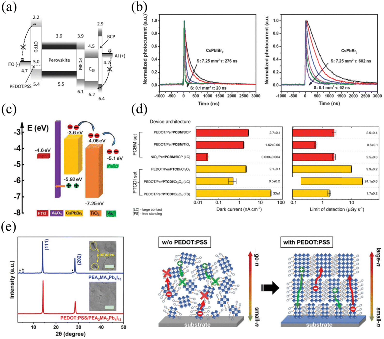 | ||
| Fig. 10 (a) Energy diagram of the cross-linked OTPD MHPPDs. Reproduced with permission.10 Copyright 2015, Wiley-VCH. (b) Transient response curves of the inorganic MHPPDs with PTAA/PEIE. Reproduced with permission.106 Copyright 2018, Wiley-VCH. (c) Energy band diagram of the MHPPDs with ultrathin Al2O3 and TiO2 modification layers. Reproduced with permission.107 Copyright 2019, Wiley-VCH. (d) Summary of the interface engineering based on several organic materials. Reproduced with permission.108 Copyright 2020, Wiley-VCH. (e) XRD patterns of quasi-2D thin films without and with PEDOT:PSS interlayer (left), the insets are the corresponding top-view FESEM images (scale bar: 1 μm), and schematic illustration of the orientational growth of MHP films without/with PEDOT:PSS interlayer. Reproduced with permission.109 Copyright 2023, Wiley-VCH. | ||
In addition to organic interface layers, inorganic oxide layers deposited using atomic layer deposition (ALD) show promise for suppressing Jd and enabling ultra-fast MHPPDs. Cen et al. utilized ALD to fabricate CsPbBr3-based MHPPDs with Al2O3 and TiO2 interfacial layers107 (Fig. 10c). These layers significantly reduced current leakage by more than three orders of magnitude, leading to the successful realization of robust visible light communication systems. The investigation of organic CTLs for MHPPDs in X-ray detection has also been explored. Demchyshyn and co-workers employed PCBM and PTCDI as the HBL and PEDOT:PSS and NiOx as the hole transport layer in a P–I–N MHPPD structure using (Cs0.05(FA0.83MA0.17)0.95PbI3−xBrx) as the high energy photon absorption layer.108 The results demonstrated different performance characteristics for different configurations, with the lowest Jd (0.030 ± 0.004 nA cm−2) achieved in the NiOx/MHP/PCBM/BCP configuration and the lowest detection limit (0.58 ± 0.05 μGy s−1) in the PEDOT/MHP/PCBM/TiOx configuration. (Fig. 10d) Furthermore, Zhang et al. investigated the importance of PEDOT:PSS and PC71BM in quasi-2D PEA2MA3Pb4I13-based MHPPDs for UV-A region detection.109 The inclusion of PEDOT:PSS as the substrate enhanced the vertical orientation of PEA2MA3Pb4I13, as indicated by a smoother XRD pattern. (Fig. 10e) The uniform crystalline morphology and gradient phase distribution of quasi-2D MHPPDs obtained here exhibit a respectable D* of 1.3 × 10¹² Jones, along with a swift speed of 313 μs/40.8 ms. Furthermore, extensive efforts have been directed towards introducing new CTLs and modifying both organic and inorganic CTLs to effectively passivate surface defects, construct cascades, and suppress Jd, thereby enhancing the performance of MHPPDs, as outlined in Table 4.
| Strategy | Device structure | Dark current (density) (Id or Jd) | D* (Jones) | Speed [rise time (tr)/fall (decay) time (tf)] | LDR (dB) | Ref. |
|---|---|---|---|---|---|---|
| a Noise signal: the noise signal in photodetection is recorded by utilizing a fast Fourier transform signal analyzer combined with a preamplifier to capture the noise current at various frequencies. b TPC extracted: speed here can be defined as the time at which the photocurrent decays from the peak to the original 1/e extracted from the transient photocurrent curves. c Detection limit: the detection limit in X-ray detection is defined as the equivalent dose rate to produce a photocurrent greater than three times the noise current (dark current). | ||||||
| Reduce surface defects and regulate band alignment (silane barrier-capped MAPbBr3 quantum dots as an HBL) | ITO/PEDOT:PSS/MHP/silane barrier-capped MAPbBr3 quantum dot/PC70BM/Ag | 2.19 × 10⁻⁷ A cm−2 (0 V, about 2.5 times reduced) | 7.85 × 10¹² | — | — | 110 |
| Reduce surface defects (3,4,5-tris (n-dodecyloxy)benzoylamide with an azobenzene moiety (TBA-Azo) additives for Sn–Pb MHP) | ITO/PTAA/MHP/TBA-Azo/C60/BCP/Cu | 9.61 × 10⁻⁵ mA cm−2 (−0.1 V, about 100 times reduced) | 2.21 × 10¹¹ (758 nm) | 42.9 ns (TPC extracted)b | 185 | 102 |
| Regulate band alignment, increase optical absorption and reduce surface defects (l 2,2′-((2Z,2′Z)-((5,5′-(4,4,9,9-tetrakis(4-hexylphenyl)-4,9-dihydro-s-indaceno[1,2-b:5,6-b′]dithiophene-2,7-diyl)bis(4-((2-ethylhexyl)-oxy)thiophene-5,2-diyl))bis(methanylylidene))bis(3-oxo-2,3-di-hydro-1H-indene-2,1-diylidene))dimalononitrile (IEICO) as an interlayer | ITO/PTAA/MHP/IEICO/C60/BCP/Cu | 2.6 × 10⁻⁵ mA cm−2 (−0.1 V, about 1000 times reduced) | 1.45 × 10¹² (650 nm) | 27 ns (TPC extracted)b | 198 | 111 |
| Reduce interface defects and form interfacial dipole (brominated (3-aminopropyl)triethoxysilane (APTES) as an interlayer) | Si/APTES/MHP/C60/BCP/Au | 23 nA cm−2 (−1 V) | 9.5 μGyair s−1 (detection limit)c | —/255 μs | — | 112 |
| Regulate band alignment and reduce interface defects (NiOx:PbI2 nanocomposites as an EBL) | ITO/NiOx:PbI2/MHP/C60/BCP/Ag | 2 × 10⁻¹⁰ A cm−2 (−0.2 V) | 1013 | 168 ns (TPC extracted)b | 112 | 113 |
| Regulate band alignment and reduce surface defects (MAPbI3/poly[(2,6-(4,8-bis(5-(2-ethylhexyl)thiophen-2-yl)-benzo[1,2-b:4,5-b′]dithiophene))-alt-(5,5-(1′,3′-di-2-thienyl-5′,7′-bis(2-ethylhexyl)benzo[1′,2′-c:4′,5′-c′] dithiophene-4,8-dione)](PBDB-T):dithienocyclopenta-thieno[3,2-b] thiophene core end-capped with 1,1-dicyano-methylene-3-indanone unit (IHIC)) | ITO/TAPC/MHP/PBDB−T: IHIC/PC61BM/Ag. | 1.01 × 10⁻⁴ mA cm−2 (−0.05 V, about 4 times reduced) | 2.17 × 10¹² (600 nm) | <400 ms | — | 114 |
| 2.61 × 10¹² (740 nm) | ||||||
| Regulate band alignment and increase optical absorption (FAPb0.5Sn0.5I3/tin monosulfide quantum dots) | ITO/PEDOT:PSS/MHP/PC71BM/BCP/Ag | 13.7 pA Hz−1/2 (noise signal)a (about 2.5 times reduced) | 2.57 × 10¹² (850 nm) | 29.3/11.7 μs | 106.8 | 115 |
| Regulate band alignment and suppress electrochemical reaction (BCP as an interfacial layer between MHP and Al) | Au/Al/BCP/C60/MHP/Au | 3 nA (100 V mm−1) | 15 nGyair s−1 (detection limit)c | 7.75/8.79 ms | — | 116 |
| Regulate band alignment and reduce interface defects (poly[4-(10H-phenothiazin-10-yl)-N,N-bis(4-methoxyphenyl)aniline] (PPZ-TPA) as an EBL) | ITO/PPZ-TPA/MHP/C60/BCP/Cu | 1.26 × 10⁻⁷ A cm−2 (−0.1 V, about 10 times reduced) | 2.46 × 10¹¹ (730 nm) | 0.18 μs (TPC extracted)b | — | 117 |
| Regulate band alignment and reduce interface defects (Spiro-OMeTAD:CsI complex) | ITO/SnO2/MHP/Spiro-OMeTAD/MoO3/Cu | 9.72 × 10⁻¹⁰ A cm−2 | 2.7 × 10¹³ | 54.1/10.7 μs | 126 | 118 |
| Regulate band alignment (PMMA:Au nanocomposites as an interlayer) | ITO/PEDOT:PSS/MHP/ZnO/PMMA:Au/CuSeN/MHP/ZnO/Ag tandem device | (about 1000 times reduced) | 2.7 × 10¹⁵ (532 nm) | 631/452 ms | — | 119 |
| Regulate band alignment (graphene as a transparent conductive electrode and MoS2 as an EBL) | Graphene/MoS2/MHP/OCBM/BCP/Al | — | 7.99 × 10¹⁰ | 0.7–0.9/0.4–0.6 s | 117 | 120 |
| Reduce interface defects and optimize morphology (cross-linked PVK as an EBL) | ITO/cross-linked PVK/MHP/C60/BCP/Cu | 5.23 × 10⁻⁴ mA cm−2 (−0.1 V, about 2 times reduced) | 2.06 × 10¹¹ (730 nm) | 0.47 ms (TPC extracted)b | — | 121 |
| Regulate band alignment, reduce interface defects and optimize morphology (triazine-Th-OMeTAD as an EBL) | ITO/PEDOT:PSS/Triazine-Th-OMeTAD/MHP/PCBM/BCP/Ag | 1.09 nA cm−2 (0 V) | 8.2 × 10¹² | 18 ns (TPC extracted)b | 166 | 122 |
| Optimize morphology and crystallinity, and reduce interface defects (F4-TCNQ-modified NiOx interlayer) | ITO/NiOx/F4-TCNQ/MHP/BCP/C60/Cu | 1.5 × 10⁻¹⁰ A cm−2 (0 V, about 1.5 times reduced) | 7.2 × 10¹³ | 68.2/11.6 μs | 127.1 | 123 |
| Regulate band alignment and reduce interface defects (PEDOT:PSS as an EBL and the solvent optimization) | ITO/PEDOT:PSS/MHP/PC71BM/Ag | — | 1.3 × 10¹² (330 nm) | 313 μs/40.8 ms | — | 109 |
| Reduce interface defects and optimize morphology (PMMA insertion between NiOx and MHP) | ITO/NiOx/PMMA/MHP/PCBM/ZnO/Al | From 5.9 to 5.6 × 10⁻⁸ mA cm−2 (0 V) | 4.5 × 10¹³ | 52/18 μs | 129 | 124 |
| Regulate band alignment (PFN as an HBL) | ITO/PEDOT:PSS/MHP/PCBM/PFN/Al | <1 pA Hz−1/2 (noise signal)a | 4 × 10¹⁴ | 180/160 ns | >100 | 125 |
| Reduce interface defects and optimize crystallinity (Mg doped NiO as an EBL) | ITO/Mg-doped NiO/MHP/C60/BCP/Cu | 2.2 × 10⁻⁹ A cm−2 (−0.1 V, about 3 times reduced) | 5.3 × 10¹³ (640 nm) | 115.32/11.30 μs | 124 | 126 |
| Regulate band alignment, reduce interface defects and increase optical absorption (CuInSe2 quantum dots: PEDOT:PSS as a hybrid EBL) | ITO/CuInSe2 quantum dots: PEDOT:PSS/MHP/PCBM/Ag | — | 1.02 × 10¹³ (580 nm) | <0.02 s | 132 | 127 |
| Regulate band alignment and optimize crystallinity (NiOx as an EBL) | ITO/NiOx/MHP/PCBM/ZnO/BCP/Al | 7.84 × 10⁻⁶ mA cm−2 (0 V, about 4 times reduced) | 3.6 × 10¹¹ | 0.9/1.8 ms | — | 128 |
| Regulate band alignment and optimize crystallinity (PEDOT:PSS/PTAA as a double-EBL) | ITO/PEDOT:PSS/PTAA/MHP/PCBM/Phen-NaDPO/Ag | 2.3 × 10⁻²⁷ A2 Hz−1 (noise signal)a | 2.3 × 10¹³ (660 nm) | 2.89/1.93 μs | 156 | 129 |
| Optimize crystallinity (Nafion modified PEDOT:PSS EBL) | ITO/PEDOT:PSS/Nafion/MHP/PCBM/Al | — | 2.54 × 10¹¹ (395 nm) | 15.7/15.5 μs | — | 130 |
| Optimize morphology and crystallinity (PEIE modified PTAA substrate) | ITO/PTAA/PEIE/MHP/PCBM/BCP/Ag | 6.0 × 10⁻⁶ mA cm−2 (−0.3 V, about 600 times reduced) | 9.7 × 10¹² (525 nm) | 20 ns (TPC extracted)b | 200 | 106 |
| Regulate band alignment (introduction of TiO2 and Spiro-OMeTAD as interfacial layers) | FTO/TiO2/MHP/Spiro-OMeTAD/Au | <10−13 A Hz−1/2 (noise signal)a | 1.13 × 10¹³ | 460/556 ns | 132 | 131 |
| Regulate band alignment and reduce interface defects (PVP modified SnO2 as an HBL) | ITO/SnO2/PVP/MHP/Spiro-OMeTAD/Au | 1.8 × 10⁻⁸ mA cm−2 (−0.05 V, about 10 times reduced) | 1.2 × 10¹² (450 nm) | 3/6 μs | 80 | 132 |
| Regulate band alignment, reduce interface defects and optimize morphology (ALD TiO2/Spin-coated TiO2 as HBLs) | FTO/Bi-TiO2/MHP/Ag | 10−10 A (0 V, about 100 times reduced) | 1012 | 6.8/5.5 μs | 135.2 | 133 |
| Regulate band alignment and promote band bending (P3HT-COOH as an EBL) | ITO/P3HT-COOH/MHP/PCBM/PEI/Ag | 0.042 × 10⁻⁶ A cm−2 (−0.1 V, about 38 times reduced) | 1013 | 95 ns | 200 | 134 |
| Regulate band alignment (PEDOT:PSS or NiOx as an EBL, PCBM or PTCDI as an HBL) | ITO/PEDOT:PSS or NiOx/MHP/PCBM or PTCDI/TiO2/Al | 0.030 ± 0.004 nA cm−2 | 0.58 ± 0.05 μGy s−1(detection limit)c | — | — | 108 |
| Regulate band alignment (TiN as a blocking layer between MHP and electrode) | ITO/PTAA/PVP/MHP/PCBM/C60/TiN/Ag | 3.25 × 10⁻¹¹ A cm−2 (−0.5 V) | 1.21 × 10¹⁴ (720 nm) | 105.7/106.7 μs | 164 | 135 |
| Regulate band alignment (PCBM:PMMA as an HBL) | ITO/PEDOT:PSS/MHP/PCBM:PMMA/Al | 2.3 × 10⁻⁶ mA cm−2 (−0.01 V, about 65 times reduced) | 1.1 × 10¹³ (532 nm) | 3.0/2.2 μs | 112 | 136 |
| Optimize morphology and crystallinity, and regulate band alignment (Al2O3 and TiO2 as interfacial modification layers) | FTO/Al2O3/MHP/TiO2/Au | 10−11 A (about 1000 times reduced) | 1.88 × 10¹³ (405 nm) | 28/270 μs | 172.7 | 107 |
| Regulate band alignment and reduce interface defects (rGO:TS-CuPc nanocomposites as the interfacial layer) | ITO/rGO:TS-CuPc/MHP/PCBM/BCP/Ag | 2.2 × 10⁻⁸ A cm−2 (−0.1 V, about 10 times reduced) | 4.2 × 10¹² | <47/47 ms | 118 | 137 |
| Regulate band alignment, optimize morphology and reduce interface defects (NiOx and TiO2 as interfacial layers) | ITO/NiOx/MHP/TiO2/Au | 10−11 A (about 104 times reduced) | 1.59 × 10¹³ | 0.056/0.25 ms | 186.7 | 138 |
| Regulate band alignment and reduce surface defects (OTPD as an EBL and PCBM/C60 as HBLs) | ITO/OTPD/MHP/PCBM/C60/BCP/Al | 9.1 × 10⁻⁹ A cm−2 (−2 V, about 50 times reduced) | 7.4 × 10¹² (680 nm) | 0.12 μs (TPC extracted)b | 94 | 10 |
| Regulate band alignment (NiOx as an EBL) | ITO/PEDOT:PSS or NiOx/MHP/C60/BCP/Au | — | 12 μGy s−1 (detection limit)c | 248/— ms | — | 139 |
| Regulate band alignment and reduce interface defects (TiO2/PCBM as HBLs) | ITO/TiO2/PC61BM/MHP/P3HT/MoO3/Ag | — | 4 × 10¹² (500 nm) | 500 ns (estimated) | 100 | 140 |
| Optimize morphology, regulate band alignment and reduce interface defects (TiO2 as an HBL) | FTO/TiO2/MHP/Au | — | 3.39 × 10¹¹ (405 nm) | 0.57/0.58 ms | 128.6 | 141 |
| Reduce surface defects and regulate band alignment (P3HT as an EBL) | ITO/ZnO/MHP/P3HT/MoO3/Ag | — | 1.8 × 10¹² (640 nm) | — | 86 | 142 |
| Regulate band alignment (PCBM/C60 as HBLs) | ITO/PEDOT:PSS/MHP/PCBM/C60/LiF/Au | 5 × 10⁻¹⁰ A cm−2 (−0.5 V) | 1012 | 1.7/1.0 μs | 230 | 105 |
| Reduce interface defects and optimize morphology and crystallinity (Al2O3 as a bottom interlayer and PMMA as a surface interlayer) | ITO/PTAA/Al2O3/MHP/PMMA/PCBM/BCP/Ag | 1.5 × 10⁻¹⁴ A Hz−1/2 (noise signal)a | 5.4 × 10¹² (532 nm) | 597 ns(TPC extracted)b | 160 | 143 |
| Regulate band alignment (TiO2, Al2O3, PCBM as HBLs) | FTO/TiO2, Al2O3, PCBM/MHP/Spiro-OMeTAD/Ag,Au | 0.012 ± 0.005 μA cm−2 | (6.0 ± 1.3) × 1012 | 1.2/3.2 μs | — | 31 |
| Reduce interface defects (Li doped VOx as an EBL) | ITO/Li doped VOx/MHP/PCBM/BCP/Ag | 3.38 × 10⁻⁹ A cm−2 (−0.1 V, about 270 times reduced) | 1.23 × 10¹³ | 0.29 μs (TPC extracted)b | 113 | 144 |
| Reduce surface defects (PCBM and aluminum doped ZnO as HBLs) | ITO/PEDOT:PSS/MHP/PCBM/AZO/Al | 1.4 × 10⁻⁷ A cm−2 (−1 V) | — | 100 ns (TPC extracted)b | 57 | 145 |
| Optimize morphology (PC60BM or PC70BM as HBLs) | ITO/PEDOT:PSS/MHP/PC60BM or PC70BM/BCP/Ag | 33.41 fA Hz−1/2 (noise signal)a | 2.05 × 10¹² | 150.2/159.7 ns | >90 | 146 |
| Reduce surface defects (Cs0.1MA0.3FA0.6)AgBiI6 as an interface layer for Cs0.05MA0.65FA0.3PbI3) | ITO/NiOx/MHP/SnO2/Au | 17.5 pA cm−2 | 0.43 μGy s−1 (detection limit)c | 0.2/0.5 s | — | 147 |
5.5 Heterojunctions
Forming heterojunctions with MHPs, either by using MHPs themselves or other semiconductors with superior optoelectronic properties, offers significant advantages. These heterojunctions suppress unwanted current leakage by constructing P–N junctions and enhance device performance in several ways. They expand the photoresponse range by incorporating additional photoresponsive materials and improve stability by protecting the MHPs. Zhang et al. demonstrated a solution-based epitaxial method for the controlled fabrication of MHP single crystal heterojunctions, including MAPbBr3/MAPbI3 and MAPbCl3/MAPbBr3 heterojunctions.148 The epitaxial growth process is illustrated in Fig. 11a. By analyzing the PL properties of different locations along the cross-section of the MHP single crystal heterojunction, the researchers confirmed the controllable gradual conversion from p-type (MAPbI3) to n-type (MAPbBr3) characteristics (Fig. 11b). The high-quality MHP single crystal heterojunctions with a gradient energy band structure at the heterointerface (Fig. 11b) enabled the optimized MHPPDs to achieve low detection limits for direct X-ray detection and minimal Jd drift. Likewise, Liu and colleagues employed an epitaxial method through vapor-phase deposition to establish a monocrystalline CsPbBr3 (p-type)–SrTiO3 (n-type) halide-oxide perovskite P–N heterojunction, as depicted in Fig. 11c.149 The inclusion of rigid SrTiO3 not only increased device stability by preventing anion interdiffusion between CsPbBr3 and SrTiO3, leading to an effective operating temperature of 150 °C for the MHPPD, but also facilitated the formation of a sharp P–N interface with CsPbBr3, ensuring low Jd and satisfactory photoresponse. Furthermore, Wang et al. demonstrated a P–I–N heterojunction (n-type, Bi-doped MAPbBr3)/(intrinsic, MAPbBr2.5Cl0.5)/(p-type, Ag-doped MAPbBr3) by a solution-processed dopant incorporated epitaxial growth method.150 To identify suitable dopants, researchers investigated the thermal-probe-induced effects of MHPs incorporating different dopants. After optimization, 0.1 M AgBr-doped and 0.2 M Bi-doped MAPbBr3 were grown on opposite faces of the MAPbBr2.5Cl0.5 substrate to form a P–I–N heterojunction (Fig. 11d). Benefiting from the efficient P–I–N junction, which provides sufficient charge barriers and facilitates energy alignment, the MHPPDs exhibited a low Jd of 11 nA cm−2 under 500 V cm−1 and a lowest detection limit of 16 nGy s−1. More recently, Zou and colleagues developed a dual-band heterojunction configuration of MAPbBr3/PCBM/FASn0.5Pb0.5I3 using a high-throughput blading method for ultra-fast MHz imaging and communication speeds (Fig. 11e).151 This dual-band heterojunction, benefiting from the absorption of both wide (MAPbBr3) and narrow (FASn0.5Pb0.5I3) MHPs and tuning of the polarity and amplitude of the bias voltage, enabled MHPPDs based on this structure to achieve a D* of 1.25/3.10 × 1012 Jones and bandwidths of 16.5/>20 MHz for the visible/NIR bands. | ||
| Fig. 11 (a) Epitaxial growth process of the MHP heterojunction. (b) Positions for PL measurements (left), PL spectra (middle), and band diagram of the MHP heterojunction without bias (right). Reproduced with permission.148 Copyright 2023, Wiley-VCH. (c) Schematic diagram of the vapor-phase epitaxy of the CsPbBr3 thin film on halide–oxide perovskite. Reproduced with permission.149 Copyright 2023, Wiley-VCH. (d) Energy diagram and the fabrication process of the MHP heterojunction by doping in the epitaxial growth. Reproduced with permission.150 Copyright 2021, Elsevier. (e) Optoelectronic properties of the double MHP heterojunction thin films. Reproduced with permission.151 Copyright 2024, Wiley-VCH. | ||
Additionally, researchers have developed MHP heterojunctions incorporating narrow band gap ionic dyes (Fig. 12a) and QDs (Fig. 12b) to extend light absorption deep into NIR regimes and effectively suppress device Jd through precise gradient energy alignment design.152,153 For the UV regime of the heterojunction in MHPPDs, Ga2O3 (Fig. 12c) and ZnO (Fig. 12d) were employed to achieve efficient carrier separation and broaden the photoresponse of MHPPDs.154,155Table 5 compares the performance parameters of recent MHPPDs based on various heterojunctions.
 | ||
| Fig. 12 (a) Photoresponse of the CyPF6, Cy1BF4, and MHP-CyPF6, Cy1BF4 heterojunction MHPPDs. Reproduced with permission.152 Copyright 2017, Wiley-VCH. (b) Energy band diagram of the MHP/CuInSe2 QDs heterojunction (left), the absorption and PL spectra of the MHP/CuInSe2 QD thin film (right). Reproduced with permission.156 Copyright 2020, Wiley-VCH. (c) Absorption spectrum and bandgap of MAPbCl3 and amorphous Ga2O3 films (left), the I–t curves of the MAPbCl3/amorphous Ga2O3-based devices (right). Reproduced with permission.157 Copyright 2022, Elsevier. (d) Energy band diagram showing the band alignment and carrier dynamics of the CsSnI6/ZnO device under different biases. Reproduced with permission.155 Copyright 2020, RSC. | ||
| Strategy | Device structure | Dark current (density) (Id or Jd) | D* (Jones) | Speed [rise time (tr)/fall (decay) time (tf)] | LDR (dB) | Ref. |
|---|---|---|---|---|---|---|
| a Noise signal: the noise signal in photodetection is recorded by utilizing a fast Fourier transform signal analyzer combined with a preamplifier to capture the noise current at various frequencies. b TPC extracted: speed here can be defined as the time at which the photocurrent decays from the peak to the original 1/e extracted from the transient photocurrent curves. c Detection limit: the detection limit in X-ray detection is defined as the equivalent dose rate to produce a photocurrent greater than three times the noise current (dark current). d Drifting: drifting means the dark current drift period D. | ||||||
| Generate injection barrier and reduce interface defects (MAPbBr3/Bi3+-doped MAPbCl3 single crystals) | Au/MAPbBr3/Bi3+-doped MAPbCl3/Au | 0.78 nA (−100 V) | — | 4.89 μs (TPC extracted)b | — | 159 |
| Establish the built-in electrical field (electrochemical-deposition NiOx/Cs3Bi2Br9) | FTO/NiOx/MHP/Ag | 1.3 × 10⁻¹² A Hz−1/2 (noise signal)a | 1.3 × 10¹¹ | 3.04/4.66 ms | 116.6 | 160 |
| Establish the built-in electrical field (CsPbBr3/Cs4PbBr6) | ITO/SnO2/CsPbBr3/Cs4PbBr6/P3HT:PCBM/Au | 63 nA cm−2 (4 V, about 1.3 times reduced) | 15 nGys−1 (detection limit)c | 1.6/1.2 ms | — | 156 |
| Regulate band alignment (GaN/Cs2AgBiBr6/NiO) | In/GaN/MHP/NiO/Au | 1.89 × 10⁻⁹ A (0 V) | 3.28 × 10¹¹ (365 nm) | 151/215 μs | — | 157 |
| Establish the built-in electrical field (MAPbCl3/Bi3+-doped MAPbCl3 single crystals) | Ag/MAPbCl3/Bi3+-doped MAPbCl3 single crystals/Au | 2.15 μA cm−2 (−20 V) | 4.87 × 10¹¹ (393 nm) | 176.3 ns/11.6 μs | — | 158 |
| Establish the built-in electrical field (PVP-modified MAPbCl3−xIx/Si) | Au/MHP/Si/Au | — | 1.5 × 10¹² (405 nm) | 645/560 μs | 44 | 161 |
| Establish the built-in electrical field (planar-type Ag+-doped MAPbBr3/Sb3+-doped MAPbBr3) | Pt/Ag+-doped MAPbBr3/Sb3+-doped MAPbBr3/Ag | 300 fA Hz−1/2 (0 V) | 6.39 × 10¹¹ (530 nm) | 14/10 ms | — | 162 |
| Establish the built-in electrical field (MAPbBr2.5Cl0.5/MAPbCl3) | Au/Poly-TPD/MAPbBr2.5Cl0.5/MAPbCl3/Ag | 1.12 × 10⁻¹⁰ A Hz−1/2 (noise signal)a (−100 V) | 7.32 × 10⁷ (500 nm) | 10/15 μs | — | 163 |
| Establish the built-in electrical field (ZnO/Cs2SnI6) | ITO/ZnO/MHP/Al | 0.15 pA Hz−1/2 | 1.39 × 10¹² (378 nm) | 4.3/5.2 μs | 119 | 155 |
| 5.88 × 10¹¹ (858 nm) | ||||||
| Establish the built-in electrical field (Si/SnO2/MAPbI3/MoO3) | Al/Si/SnO2/MAPbI3/MoO3/Ag | 0.13 nA | 2.23 × 10¹² (815 nm) | 13.0/14.6 ms | — | 164 |
| Establish the built-in electrical field (ZnO/PTAA/MAPbCl3) | ITO/ZnO/MHP/PTAA/MoOx/Ag | 5.46 fA Hz−1/2 (about 20% reduced) | 6.07 × 10¹¹ (390 nm) | 28/— μs | — | 165 |
| Reduce interface defects and regulate band alignment (2D/3D MHP/O6T-4F) | ITO/PTAA/MHP/O6T-4F/C60/BCP/Al | 3.57 × 10⁻¹⁰ mA cm−2 (−0.5 V, about 8 times reduced) | 1.06 × 10¹⁵ (500 nm) | 2.9/4.8 μs | 110 | 166 |
| Establish the built-in electrical field (MAPbI3/TiO2) | FTO/TiO2/MHP/Spiro-OMeTAD/Au | −5 nA (0 V) | 7.8 × 10¹⁰ (494 nm) | — | — | 167 |
| Establish the built-in electrical field ((BA)2(MA)Pb2I7/(BA)2PbI4/(BA)2(MA)Pb2I7) | ITO/MHPs/Cr/Au | 10−6 A cm−2 (about 103 times reduced) | — | 150/170 ms | — | 168 |
| Establish the built-in electrical field and increase optical absorption (NiO/MAPbI3) | FTO/MHP/NiO/Au | — | 1010 | 320 ± 10/305 ± 10 ms | — | 169 |
| Regulate band alignment and increase optical absorption (CuInSe2 quantum dots/MAPbI3) | FTO/PEDOT:PSS/CuInSe2 quantum dots/MHP/PCBM/Ag | 8.7 fA Hz−1/2 (noise signal)a | 7.0 × 10¹⁰ (580 nm) | 277 ns (TPC extracted)b | 75.16 | 153 |
| 7.7 × 10¹¹ (850 nm) | ||||||
| Establish the built-in electrical field and impede the anion interdiffusion (CsPbBr3/SrTiO3) | Au/CsPbBr3/SrTiO3/Ag | 2.01 × 10⁻¹² A (−1 V) | 2.98 × 10¹³ | 2.06/0.30 s | — | 149 |
| Establish the built-in electrical field (SnO2/Cs2AgBiBr6) | FTO/SnO2/MHP/Au | 2 nA (about 280 times reduced) | 2.1 × 10¹² | 248/341 μs | 108 | 170 |
| Reduce interface defects and increase optical absorption (MAPbI3/PDPPTDTPT:PCBM) | ITO/PTAA/MHP/PDPPTDTPT:PCBM/BCP/Cu | 8.7 × 10⁻⁵ mA cm−2 (−0.3 V, about 100 times reduced) | 1 × 10¹¹ (900 nm) | 5 ns (TPC extracted)b | 95 | 171 |
| Establish the built-in electrical field (MAPbI3/PTB7/C60) | ITO/PEDOT:PSS/MHP/PTB7/C60/BCP/Ag | 1.85 × 10⁻⁵ mA cm−2 (−0.1 V) | 1.37 × 10¹² (680 nm) | 3.9/4 μs | 141 | 172 |
| Establish the built-in electrical field (MAPbBr3−nCln/CsPbBr3) | Au/MAPbBr3−nCln/CsPbBr3/Au | 0.5 μA cm−2 | 96 nGy s−1 (detection limit)c | — | — | 173 |
| 3.92 × 10⁻⁴ nA cm−1 s−1 V−1 (drifting)d | ||||||
| (−125 V mm−1, about 100 times reduced) | ||||||
| Establish the built-in electrical field (MAPbCl3/MAPbBr3 single crystal) | Au/MAPbCl3/MAPbBr3/Au | 300 nA (about 5 times reduced) | 7 × 10¹¹ | 0.43/1.39 s | — | 174 |
| Establish the built-in electrical field (Bi-doped MAPbBr3/MAPbBr2.5Cl0.5/Ag-doped MAPbBr3) | Au/Bi-doped MAPbBr3/MAPbBr2.5Cl0.5/Ag-doped MAPbBr3/Au | 11 nA cm−2 (−0.07 V) | 16 nGy s−1 (detection limit)c | —/750 ns | — | 150 |
| Establish the built-in electrical field and regulate band alignment (MAPbCl3/MAPbBr3 single crystal) | Au/MAPbCl3/MAPbBr3/Au | — | 12.2 nGy s−1 (detection limit)c | 1.5/1.6 ms | — | 148 |
| Establish the built-in electrical field (Cs2AgBiBr6/(C38H34P2)MnBr4) | Au/Cs2AgBiBr6/(C38H34P2)MnBr4/C60/BCP/Cr | 20 pA Hz−1/2 (noise signal)a | 0.2 μGy (detection limit)c | 41 ns (TPC extracted)b | — | 175 |
| 5.3 × 10⁻⁷ nA cm−1 s−1 V−1 (drifting)d | ||||||
| (1000 V mm−1) s−1 | ||||||
| Regulate band alignment and establish the built-in electrical field (Cs0.15FA0.85Pb(I0.15Br0.85)3/Cs0.15FA0.85PbI3) | Carbon/Cs0.15FA0.85Pb(I0.15Br0.85)3/Cs0.15FA0.85PbI3/C60/BCP/Cr | 0.701 nA cm−2 (−25 V, about 200 times reduced) | 13.8 ± 0.29 nGy s−1 (detection limit)c | 6.1 μs | — | 176 |
| Establish the built-in electrical field (MAPbI3/PDPP3T:PC71BM) | ITO/PEDOT:PSS/MHP/PDPP3T:PC71BM/Al | 3.6 × 10⁻⁹ A cm−2 (−0.1 V, about 5 times reduced) | 3 × 10¹³ | 4.82/4.30 μs | 112 | 177 |
| Establish the built-in electrical field and increase optical absorption (MAPbI3:graphene quantum dots/Porous Si) | InGa/BCP/Si/P-Si/MHP/Au | — | 7.6 × 10¹⁰ | 654/735 ns | 80 | 178 |
| Establish the built-in electrical field and increase optical absorption (MAPbCl3/amorphous Ga2O3) | FTO/Ga2O3/MHP/Spiro-OMeTAD/Ag | 1.042 nA (about 330 times reduced) | 5.4 × 10¹⁰ | 56/67 ms | 80 | 154 |
| Establish the built-in electrical field and increase optical absorption (MAPbBr3/FASn0.5Sn0.5I3) | FTO/PEDOT:PSS/MHP/PCBM/MHP/P3HT/Ag | 1.3 × 10⁻¹⁰ mA cm−2 (−0.5 V, 7000 times reduced) | 1.25 × 10¹² | 124.5/37.2 ns | 102 | 151 |
| Establish the built-in electrical field and increase optical absorption (MHP/ternary BHJ (FAPbI3/PM6:BTP-eC9:BTP-2F2Cl-P2TH)) | ITO/SnOx/MHP/PM6:BTP-eC9:BTP-2F2 | 3.74 nA cm−2 (−0.2 V) | >1013 (800–900 nm) | 9.02/11.42 μs | — | 179 |
| Cl-P2TH/C60/BCP/Ag | >1012 (400–800 nm) | |||||
5.6 Architecture modification
The device architecture plays a crucial role in reducing Jd and enhancing the FOMs of MHPPDs. By controlling the stacking type of materials, manipulating the electrodes, and incorporating extra devices into the MHPPDs, it is possible to efficiently mitigate Jd and increase the FOMs of MHPPDs. For example, Song et al. designed lateral P–I–N single crystal MHPPDs to isolate the electrodes from contacting the MHP surface, in contrast to conventional metal–semiconductor–metal photodiodes, as illustrated in Fig. 13a.180 The resulting devices exhibited nearly three orders of magnitude suppression of Jd compared to the metal–semiconductor–metal devices. Moreover, they demonstrated environmental stability by avoiding the interfacial electrochemical reaction between the electrode and MHP. In another approach, Jin et al. developed a MHPPD architecture by adding a shunting electrode as a blanking unit to suppress Jd.181 As depicted in Fig. 13b, electrons are emitted from the source to the drain electrode with two lateral terminals in the dark. To minimize the absolute value of Jd, a top dark-current-shunting electrode on the MHP films was utilized to attract the emitted electrons, leading to effective shunting of mobile electrons under dark conditions. This design resulted in an ultra-low Jd of 51.1 pA cm−2 and a detection limit of 7.84 nGy s−1. Additionally, Zhan et al. introduced a modification to the device structure by presenting a MHPPDs crossbar array through vapor deposition.182 This array consisted of a P–I–N diode (ITO/PEDOT:PSS/MHP/PCBM/BCP) and a reverse blocking diode (PCBM/BCP/PbI2/Spiro-TTB) in a vertically stacking sequence, with PCBM/BCP serving as the co-cathode, as shown in Fig. 13c. The presence of the blocking diode established an efficient barrier to prevent electron transfer to the Ag electrode. This configuration is fully scalable and compatible with integrated circuits, making it suitable for the industrialization of image sensors. The devices and the corresponding strategies for architecture modification and performance parameters are summarized in Table 6. | ||
| Fig. 13 (a) The schematic diagram, the energy level diagram, and dark current curves of the metal–semiconductor–metal (MSM) and lateral P–I–N devices. Reproduced with permission.180 Copyright 2021, Wiley-VCH. (b) The schematic illustration of the conventional and dark-current-shunting MHPPD under dark and X-ray radiation. Reproduced with permission.181 Copyright 2023, Nature. (c) The structure of an integrated PIN-blocking diode. (d) Current–voltage (I–V) curves of the blocking diode. Reproduced with permission.182 Copyright 2022, Wiley-VCH. | ||
| Strategy | Device structure | Dark current (density) (Id or Jd) | D* (Jones) | Speed [rise time (tr)/fall (decay) time (tf)] | LDR (dB) | Ref. |
|---|---|---|---|---|---|---|
| a Noise signal: the noise signal in photodetection is recorded by utilizing a fast Fourier transform signal analyzer combined with a preamplifier to capture the noise current at various frequencies. b TPC extracted: speed here can be defined as the time at which the photocurrent decays from the peak to the original 1/e extracted from the transient photocurrent curves. c Detection limit: the detection limit in X-ray detection is defined as the equivalent dose rate to produce a photocurrent greater than three times the noise current (dark current). | ||||||
| Regulate band alignment and promote band bending (MAPbI3 integrated with a 2D photogate photodiode) | Au/MHP/BP/MoS2 | 3 × 10⁻¹¹ A | 1.3 × 10¹² | 150/240 μs | 111 | 183 |
| Regulate band alignment and promote band bending (PIN PPDs stacked by a reverse blocking diode and the PCBM/BCP as the co-cathode) | ITO/PEDOT:PSS/MHP/PCBM/BCP/PbI2/Spiro-TTB/Ag | — | 2.1 × 10¹² (710 nm) | 61.2/72.8 ns | 112 | 182 |
| Regulate band alignment and promote band bending (asymmetric contact electrodes Ag/MAPbI3/Au) | Ag/MAPbI3/Au | 3.6 × 10⁻¹⁶ A Hz−1/2 (noise signal)a | 1.3 × 10¹² (520 nm) | 13.8/16.1 μs | — | 184 |
| Establish the built-in electrical field and manage the optical absorption (MHP-based photodiode integrated with MHP-based photoconductor) | ITO/TaTm:F6-TCNNQ/MHP/TaTm:F6-TCNNQ/TaTm/MHP/C60/BCP/Ag | 1.1 × 10⁻⁴ mA cm−2 (−1 V, about 8 times reduced) | 1.7 × 10¹² (730 nm) | 25.3 μs (TPC extracted)b | 63 | 185 |
| Eliminate the interfacial electrochemical reaction (lateral device BCP/C60/MAPbI3/MoO3) | Lateral Au/BCP/C60/MAPbI3/MoO3/Au | 265 pA Hz−1/2 (noise signal)a (about 103 times reduced) | 0.1 nGy s−1 (detection limit)c | 420/470 μs | — | 180 |
| Impede shunt dark current by employing a top electrode (P–I–N diode integrated a dark-current-shunting electrode) | Au (source)/C60/MHP/Au (drain) and PMMA/Au worked as the top electrode | 51.1 fA (5 V mm−1) | 7.84 nGy s−1 (detection limit)c | — | — | 181 |
6. Summary and perspectives
Due to their remarkable optical and electrical properties, MHPPDs have showcased unparalleled performance, surpassing commercially available inorganic counterparts in recent years. In addition, formidable progress has been made in developing robust optoelectronic applications such as static imaging for visible and X-ray spectra,141,186 real-time dynamic imaging,182 communications,102,107 and health monitoring.91,187 Despite this, MHPPDs still face challenges related to defects within their structure that impair the dynamics of charge carriers, diminishing photodetection performance metrics like Jd, LDR, D*, and speed. To address these issues, a deep understanding of Jd's origin in MHPPDs is critical. Research has been directed towards component and dimensional engineering to mitigate defects within the bulk and interfaces, interfacial engineering, the integration of heterojunctions, and adjustments to device architectures. Tables 1–6 encapsulate the enhancements in Jd and other FOMs demonstrated using these strategies. Future research targeting superior performance and durability in optoelectronic devices, facilitating detection across a broad spectral range from ionizing radiation to near-infrared, is indispensable. Achieving high EQE or R while simultaneously suppressing the Jd in MHPPDs is critical and challenging. Both EQE (or R) and Jd are highly dependent on carrier generation, extraction, and recombination processes. The efficiency of these processes directly impacts EQE (or R) and Jd. For instance, the quality of the MHP films and the interfaces between the MHP and the EBL as well as the HBL are essential for influencing charge transportation and recombination, thereby impacting EQE (or R) and Jd. The mobility and stability of the EBL and HBL are highly relevant to charge extraction and recombination at the interface between MHP and EBL/HBL, thereby also affecting EQE (or R) and Jd. Furthermore, mechanical stress at the interface between MHP and EBL/HBL can introduce defects that deteriorate EQE (or R) and Jd. Therefore, by employing advanced passivation techniques, improved fabrication methods, and optimized device architectures aimed at increasing the quality of the MHP film, EBL/HBL, and the interface between MHP and EBL/HBL, it is possible to develop MHPPDs with high EQE (or R) and low Jd.Central to advancing MHPPDs is an in-depth understanding of the origins of Jd. Current research predominantly employs the conventional semiconductor-based photodiode model grounded in thermodynamics. However, given MHPs' ionic characteristics, it is pivotal to develop a nuanced MHPPD model accounting for ion migration within the bulk and interfaces—an imperative for light sensing and direct radiation detection applications. A comprehensive model must also incorporate interactions between MHPs, CTLs, and electrodes to thoroughly describe charge carrier behavior under dark conditions.
Addressing the defects present in MHPs is the crucial strategy for substantially reducing the Jd in MHPPDs. These defects, located in the bulk and at the interfaces of MHPs, are recognized as major contributors to elevated Jd levels and undesirable periods of Jd drift in MHPPDs. Thankfully, numerous effective strategies have emerged which include component, additive, and interfacial engineering. Among these, strategic component selection is particularly promising in mitigating issues such as ion migration and phase transitions caused by these defects. Monovalent cations like FA are highly competitive in MHPs used in MHPPDs for broadband light detection, owing to their lower bandgap and improved thermal and light stability compared to other cations. Similarly, the choice of halide ions plays a critical role. Beyond just tuning the absorption spectrum of the devices, previous studies have highlighted the beneficial effects of various halide anions on the crystallization process and defect suppression in MHP films. Notably, Cl− and bromine Br− ions, at certain concentrations, can enhance crystallinity, morphology, and stability of MHPs, which in turn boosts photodetection performance.
Passivation techniques involving additives in MHP precursor solutions and interfacial engineering are critical for defect suppression and overall device performance enhancement. It is imperative to develop thoughtful additive design strategies and more resilient CTLs that consider the multifunctional effects of additives and the complexities of surface defect configurations. Moreover, there is a need for continued research into strategies for constructing heterojunctions either with MHPs or with other superior optoelectronic materials. These heterojunctions could help in managing surface defects, aligning energy bands, and improving optoelectronic properties, thus potentially mitigating Jd and minimizing periods of Jd drift in MHPPDs.
Further rethinking of the architecture of MHPPDs can serve to effectively suppress Jd. Introducing additional layers, such as EBL or HBL, can prevent charge carriers from being injected from the electrodes into the MHP, thereby reducing Jd. The alignment of material energy levels, as well as both vertical and lateral architectural designs, are crucial in influencing the charge dynamics within the device. Additionally, the implementation of electrical regulation methods can effectively curb Jd and further diminish Jd drift periods.181,188 Future research should focus on simplifying device structures and developing strategies suitable for large-scale industrial production.
Controlling the operational temperature of MHPPDs has shown potential in minimizing Jd and enhancing device performance. Lower temperatures effectively restrain thermal excitation of charge carriers, thereby reducing Jdiff generation. This temperature-dependent suppression offers promising prospects for achieving enhanced D* in MHPPDs. Moreover, operating at cooler temperatures can increase the stability and lifespan of MHP films by curbing degradation processes. However, maintaining an optimal temperature is essential; excessively low temperatures may impair the device's response time and sensitivity. Therefore, it is critical to finely tune the temperature range to strike a balance between suppressing Jd while sustaining overall device effectiveness.
Additionally, thorough testing and accurate characterization of MHPPDs are imperative.189 Common issues include the overestimation of D* due to the oversight of noise currents other than Jd,190 the challenges in testing MHPPDs for direct X-ray detection under atmospheric conditions,191 and incorrect application of formulas or linear fitting in assessing the LDR of MHPPDs.192 Implementing advanced characterization techniques is fundamental to elucidate the chemical, morphological, structural, and optoelectronic attributes of MHPs, which assist in mitigating Jd in MHPPDs. Techniques such as UV-visible-NIR spectroscopy, photoluminescence (PL), time-resolved PL, and transient absorption spectroscopy are instrumental in directly assessing the light absorption and luminescence properties of MHPs. Electron microscopies like scanning electron microscopy (SEM), transmission electron microscopy (TEM), atomic force microscopy (AFM) combined with conductive AFM (c-AFM), and energy-dispersive X-ray (EDX) spectroscopy provide in-depth analysis of chemical, morphological, and structural properties at the interface of MHPs. Depth-profiling techniques, including X-ray photoelectron spectroscopy (XPS) and time-of-flight secondary ion mass spectrometry (TOF-SIMS), are crucial for profiling the chemical composition through the depth of MHPs. Characterization techniques geared towards electrical properties, such as electrochemical impedance spectroscopy (EIS), space-charge-limited currents, and transient photovoltage/photocurrent studies, are critical for investigating charge transport and extraction dynamics in MHPPDs. By leveraging these advanced techniques and refining the associated methodologies, we can better differentiate the performance attributes of MHPs, address their intrinsic challenges, and drive forward the performance of MHPPDs. In conclusion, as research continues to focus on suppressing Jd and improving the reliability and functionality of MHPPDs, their practical application in the field of optoelectronics is becoming increasingly feasible.
Author contributions
Yue Wang, D. Li, and Q. Song conducted the literature review and drafted the manuscript. Yue Wang, D. Li, Yang Wang, Y. Chen contributed to manuscript editing and grammar check. Yue Wang, D. Li, Q. Song, Y. Liu, Yang Wang and Y. Chen secured funding, resources, supervision, and contributed to manuscript editing.Data availability
No primary research results, software or codes have been included and no new data were generated or analysed as part of this review.Conflicts of interest
There are no conflicts to declare.Acknowledgements
This work was supported by the Natural Science Foundation of China (Grant No. 62205062), the Natural Science Foundation of Fujian Province of China (Grant No. 2022J05047, 2023J01087, 2023J01527, 2023J01530), and the Fujian Normal University “Young Talent” Start-up Grant (Grant No. Y0720308K13).References
- Z. Li, T. Yan and X. Fang, Nat. Rev. Mater., 2023, 8, 587–603 CrossRef.
- F. Cao, L. Liu and L. Li, Mater. Today, 2023, 62, 327–349 CrossRef CAS.
- S. Mauthe, Y. Baumgartner, M. Sousa, Q. Ding, M. D. Rossell, A. Schenk, L. Czornomaz and K. E. Moselund, Nat. Commun., 2020, 11, 4565 CrossRef CAS.
- R. Tian, X. Gan, C. Li, X. Chen, S. Hu, L. Gu, D. Van Thourhout, A. Castellanos-Gomez, Z. Sun and J. Zhao, Light: Sci. Appl., 2022, 11, 101 CrossRef CAS.
- F. P. García De Arquer, A. Armin, P. Meredith and E. H. Sargent, Nat. Rev. Mater., 2017, 2, 16100 CrossRef.
- Q. Qiu and Z. Huang, Adv. Mater., 2021, 33, 2008126 CrossRef CAS.
- W. Ouyang, J. Chen, Z. Shi and X. Fang, Appl. Phys. Rev., 2021, 8, 31315 CAS.
- G. Long, R. Sabatini, M. I. Saidaminov, G. Lakhwani, A. Rasmita, X. Liu, E. H. Sargent and W. Gao, Nat. Rev. Mater., 2020, 5, 423–439 CrossRef.
- Q. Lin, A. Armin, P. L. Burn and P. Meredith, Nat. Photonics, 2015, 9, 687–694 CrossRef CAS.
- Y. Fang and J. Huang, Adv. Mater., 2015, 27, 2804–2810 CrossRef CAS.
- C. Li, H. Wang, F. Wang, T. Li, M. Xu, H. Wang, Z. Wang, X. Zhan, W. Hu and L. Shen, Light: Sci. Appl., 2020, 9, 31 CrossRef CAS.
- C. Chen, Z. Wang, J. Wu, Z. Deng, T. Zhang, Z. Zhu, Y. Jin, B. Lew, I. Srivastava, Z. Liang, S. Nie and V. Gruev, Sci. Adv., 2023, 9, eadk3860 CrossRef CAS.
- S. Tie, S. Dong, R. Yuan, B. Cai, J. Zhu and X. Zheng, Chem. Commun., 2023, 59, 5016–5029 RSC.
- P. Kumar, V. K. Shukla, M. Kim and R. Singh, Sens. Actuators, A, 2024, 369, 115076 CrossRef CAS.
- Z. Xiao, Z. Song and Y. Yan, Adv. Mater., 2019, 31, 1803792 CrossRef CAS.
- G. Kakavelakis, M. Gedda, A. Panagiotopoulos, E. Kymakis, T. D. Anthopoulos and K. Petridis, Adv. Sci., 2020, 7, 2002098 CrossRef CAS.
- Q. A. Akkerman, V. D. Innocenzo, S. Accornero, A. Scarpellini, A. Petrozza, M. Prato and L. Manna, J. Am. Chem. Soc., 2015, 137, 10276–10281 CrossRef CAS.
- X. Li, J. M. Hoffman and M. G. Kanatzidis, Chem. Rev., 2021, 121, 2230–2291 CrossRef CAS PubMed.
- C. Zhou, H. Lin, Q. He, L. Xu, M. Worku, M. Chaaban, S. Lee, X. Shi, M. Du and B. Ma, Mater. Sci. Eng., R, 2019, 137, 38–65 CrossRef.
- A. Dey, J. Ye, A. De, E. Debroye, S. K. Ha, E. Bladt, A. S. Kshirsagar, Z. Wang, J. Yin, Y. Wang, L. N. Quan, F. Yan, M. Gao, X. Li, J. Shamsi, T. Debnath, M. Cao, M. A. Scheel, S. Kumar, J. A. Steele, M. Gerhard, L. Chouhan, K. Xu, X. Wu, Y. Li, Y. Zhang, A. Dutta, C. Han, I. Vincon, A. L. Rogach, A. Nag, A. Samanta, B. A. Korgel, C. Shih, D. R. Gamelin, D. H. Son, H. Zeng, H. Zhong, H. Sun, H. V. Demir, I. G. Scheblykin, I. Mora-Seró, J. K. Stolarczyk, J. Z. Zhang, J. Feldmann, J. Hofkens, J. M. Luther, J. Pérez-Prieto, L. Li, L. Manna, M. I. Bodnarchuk, M. V. Kovalenko, M. B. J. Roeffaers, N. Pradhan, O. F. Mohammed, O. M. Bakr, P. Yang, P. Müller-Buschbaum, P. V. Kamat, Q. Bao, Q. Zhang, R. Krahne, R. E. Galian, S. D. Stranks, S. Bals, V. Biju, W. A. Tisdale, Y. Yan, R. L. Z. Hoye, L. Polavarapu and G. C. U. S. National Renewable Energy Lab. Nrel and O. V. S. Univ., ACS Nano, 2021, 15, 10775–10981 CrossRef CAS.
- J. S. Manser, J. A. Christians and P. V. Kamat, Chem. Rev., 2016, 116, 12956–13008 CrossRef CAS PubMed.
- C. Neusel, H. Jelitto and G. A. Schneider, J. Appl. Phys., 2015, 117, 154902 CrossRef.
- J. Chen and N. G. Park, Adv. Mater., 2019, 31, 1803019 CrossRef CAS.
- W. Jang, K. Kim, B. G. Kim, J. S. Nam, I. Jeon and D. H. Wang, Adv. Funct. Mater., 2022, 32, 2207713 CrossRef CAS.
- J. Yang, H. Zhang, H. Cui, S. Xu, G. Pan, H. Gao, Z. Zhang and Y. Mao, ACS Photonics, 2024, 11, 1181–1188 CrossRef CAS.
- V. M. Le Corre, M. B. Johnston, L. J. A. Koster, J. Lim and H. J. Snaith, Energy Environ. Sci., 2021, 15(17), 14006–14760 Search PubMed.
- Z. Y. Yin, Y. Chen, Y. Y. Zhang, Y. Yuan, Q. Yang, Y. N. Zhong, X. Gao, J. Xiao, Z. K. Wang, J. L. Xu and S. D. Wang, Adv. Funct. Mater., 2023, 33, 2302199 CrossRef CAS.
- O. D. I. Moseley, B. Roose, S. J. Zelewski and S. D. Stranks, ACS Appl. Energy Mater., 2023, 6, 10233–10242 CrossRef CAS PubMed.
- R. Ollearo, J. Wang, M. J. Dyson, C. H. L. Weijtens, M. Fattori, B. T. van Gorkom, A. J. J. M. van Breemen, S. C. J. Meskers, R. A. J. Janssen and G. H. Gelinck, Nat. Commun., 2021, 12, 7277 CrossRef CAS PubMed.
- O. Almora, D. Miravet, I. Gelmetti and G. Garcia-Belmonte, Phys. Status Solidi RRL, 2022, 16, 2200336 CrossRef CAS.
- B. R. Sutherland, A. K. Johnston, A. H. Ip, J. Xu, V. Adinolfi, P. Kanjanaboos and E. H. Sargent, ACS Photonics, 2015, 2, 1117–1123 CrossRef CAS.
- E. A. Duijnstee, V. M. Le Corre, M. B. Johnston, L. J. A. Koster, J. Lim and H. J. Snaith, Phys. Rev. Appl., 2021, 15, 014006 CrossRef CAS.
- A. Datta, J. Fiala, P. Becla and S. Motakef, APL Mater., 2017, 5, 106109 CrossRef.
- K. T. Ho, S. F. Leung, T. Y. Li, P. Maity, B. Cheng, H. C. Fu, O. F. Mohammed and J. H. He, Adv. Mater., 2018, 30, 1804372 CrossRef.
- T. S. Ripolles, A. K. Baranwal, K. Nishinaka, Y. Ogomi, G. Garcia-Belmonte and S. Hayase, Phys. Chem. Chem. Phys., 2016, 18, 14970–14975 RSC.
- Y. Shao, Y. Fang, T. Li, Q. Wang, Q. Dong, Y. Deng, Y. Yuan, H. Wei, M. Wang, A. Gruverman, J. Shield, J. Huang and L. N. U. S. Univ. Of Nebraska, Energy Environ. Sci., 2016, 9, 1752–1759 RSC.
- S. E. J. O’Kane, G. Richardson, A. Pockett, R. G. Niemann, J. M. Cave, N. Sakai, G. E. Eperon, H. J. Snaith, J. M. Foster, P. J. Cameron and A. B. Walker, J. Mater. Chem. C, 2017, 5, 452–462 RSC.
- T. Y. Yang, G. Gregori, N. Pellet, M. Gratzel and J. Maier, Angew. Chem., Int. Ed., 2015, 54, 7905–7910 CrossRef CAS.
- M. García-Batlle, S. Deumel, J. E. Huerdler, S. F. Tedde, O. Almora and G. Garcia-Belmonte, Adv. Photonics Res., 2022, 3, 2200136 CrossRef.
- Y. Yun, G. S. Han, G. N. Park, J. Kim, J. Park, D. Vidyasagar, J. Jung, W. C. Choi, Y. J. Choi, K. Heo, J. Kang, J. S. Park, H. S. Jung and S. Lee, Adv. Mater., 2022, 34, 2206932 CrossRef CAS.
- Y. Liu, Y. Zhang, X. Zhu, J. Feng, I. Spanopoulos, W. Ke, Y. He, X. Ren, Z. Yang, F. Xiao, K. Zhao, M. Kanatzidis and S. F. Liu, Adv. Mater., 2021, 33, 2006010 CrossRef CAS.
- F. Furlan, D. Nodari, E. Palladino, E. Angela, L. Mohan, J. Briscoe, M. J. Fuchter, T. J. Macdonald, G. Grancini, M. A. Mclachlan and N. Gasparini, Adv. Opt. Mater., 2022, 10, 2201816 CrossRef CAS.
- L. Li, F. Zhang, S. Ye, X. Peng, Z. Sun, J. Lian, L. Liu, J. Qu and J. Song, Nano Energy, 2020, 71, 104611 CrossRef CAS.
- Y. Wang, D. Yang, D. Ma, D. H. Kim, T. Ahamad, S. M. Alshehri and A. Vadim, Sci. China: Mater., 2019, 62, 790–796 CrossRef CAS.
- D. Liu, B. Yu, M. Liao, Z. Jin, L. Zhou, X. Zhang, F. Wang, H. He, T. Gatti and Z. He, ACS Appl. Mater. Interfaces, 2020, 12, 30530–30537 CrossRef CAS.
- F. Yao, P. Gui, C. Chen, B. Li, R. Li, C. Tao, Q. Lin and G. Fang, ACS Appl. Mater. Interfaces, 2019, 11, 39875–39881 CrossRef CAS PubMed.
- E. Hong, D. Nodari, F. Furlan, E. Angela, J. Panidi, M. A. Mclachlan and N. Gasparini, Adv. Opt. Mater., 2024, 12, 2302712 CrossRef CAS.
- N. R. Al Amin, C. Lee, Y. Huang, C. Shih, R. Estrada, S. Biring, M. Kuo, C. Li, Y. Huang and S. Liu, ACS Appl. Mater. Interfaces, 2023, 15, 21284–21295 CrossRef CAS.
- Y. Yun, H. Cho, J. Jung, S. W. Yang, D. Vidyasagar, R. K. Gunasekaran and S. Lee, J. Mater. Sci. Technol., 2023, 152, 100–108 CrossRef CAS.
- J. Wu, L. Wang, A. Feng, S. Yang, N. Li, X. Jiang, N. Liu, S. Xie, X. Guo, Y. Fang, Z. Chen, D. Yang and X. Tao, Adv. Funct. Mater., 2022, 32, 2109149 CrossRef CAS.
- P. Gui, J. Li, X. Zheng, H. Wang, F. Yao, X. Hu, Y. Liu and G. Fang, J. Mater. Chem. C, 2020, 8, 684–6812 RSC.
- W. Wang, D. Zhao, F. Zhang, L. Li, M. Du, C. Wang, Y. Yu, Q. Huang, M. Zhang, L. Li, J. Miao, Z. Lou, G. Shen, Y. Fang and Y. Yan, Adv. Funct. Mater., 2017, 27, 1703953 CrossRef.
- D. Luo, T. Zou, W. Yang, B. Xiang, X. Yang, Y. Wang, R. Su, L. Zhao, R. Zhu, H. Zhou, T. P. Russell, H. Yu and Z. H. Lu, Adv. Funct. Mater., 2020, 30, 2001692 CrossRef CAS.
- Y. Zhao, C. Li, J. Jiang, B. Wang and L. Shen, Small, 2020, 16, 2001534 CrossRef CAS.
- S. Wang, M. Li, C. Song, C. Zheng, J. Li, Z. Li, Y. Zhang and J. Yao, Appl. Surf. Sci., 2023, 623, 156983 CrossRef CAS.
- Y. Miao, J. Wu, X. Qi, L. Yang, X. Wang, F. Zheng, F. Zhao, S. Shafique, Y. Zhu and Z. Hu, Nano Energy, 2023, 113, 108605 CrossRef CAS.
- J. Peng, Y. Xu, F. Yao, H. Huang, R. Li and Q. Lin, Matter, 2022, 5, 2251–2264 CrossRef CAS.
- L. Guo, Y. Qi, Z. Wu, X. Yang, G. Yan, R. Cong, L. Zhao, W. Zhang, S. Wang, C. Pan and Z. Yang, Adv. Mater., 2023, 35, 2301705 CrossRef CAS PubMed.
- D. S. Lee, J. H. Heo, J. K. Park, B. W. Kim, H. J. Lee, Y. M. Song and S. H. Im, ACS Appl. Mater. Interfaces, 2021, 13, 16775–16783 CrossRef CAS.
- F. Zhu, G. Lian, B. Yu, T. Zhang, L. Zhang, H. Yu, D. Cui, Q. Wang, H. Zhang, Q. Meng and C. Wong, ACS Appl. Mater. Interfaces, 2022, 14, 1526–1536 CrossRef CAS PubMed.
- R. Ollearo, A. Caiazzo, J. Li, M. Fattori, A. J. J. M. van Breemen, M. M. Wienk, G. H. Gelinck and R. A. J. Janssen, Adv. Mater., 2022, 34, 2205261 CrossRef CAS PubMed.
- J. W. Lim, H. Wang, C. H. Choi, H. Kwon, L. N. Quan, W. Park, Y. Noh and D. H. Kim, Nano Energy, 2019, 57, 761–770 CrossRef CAS.
- H. Tsai, S. Shrestha, L. Pan, H. H. Huang, J. Strzalka, D. Williams, L. Wang, L. R. Cao and W. Nie, Adv. Mater., 2022, 34, 2106498 CrossRef CAS.
- R. Li, Y. Xu, W. Li, Y. Li, J. Peng, M. Xu and Q. Lin, J. Phys. Chem. Lett., 2021, 12, 1726–1733 CrossRef CAS PubMed.
- X. He, M. Xia, H. Wu, X. Du, Z. Song, S. Zhao, X. Chen, G. Niu and J. Tang, Adv. Funct. Mater., 2022, 32, 2109458 CrossRef CAS.
- Z. Liao, L. Qiu, T. Chen, W. Qian, Y. Wang, S. Yang, T. Sun, G. Yang, A. K. Srivastava and H. Zhou, Adv. Mater. Technol., 2023, 8, 2300714 CrossRef CAS.
- L. Min, W. Tian, F. Cao, J. Guo and L. Li, Adv. Mater., 2021, 33, 2101714 CrossRef CAS.
- B. Jiang, G. Yan, Y. Xiao, Y. Yuan, C. Zhao, W. Mai and R. Hong, J. Mater. Sci., 2023, 58, 7076–7091 CrossRef CAS.
- Y. Hsiao, J. Song, H. Wu, K. Hong, C. Leu and C. Shih, J. Alloys Compd., 2021, 889, 161621 CrossRef.
- X. Zhao, Y. Wang, L. Li, L. Huang, G. Li and W. H. Sun, J. Mater. Sci., 2021, 56, 9242–9253 CrossRef CAS.
- Z. Yang, M. Wang, J. Li, J. Dou, H. Qiu and J. Shao, ACS Appl. Mater. Interfaces, 2018, 10, 26387–26395 CrossRef CAS.
- H. L. Zhu, H. Lin, Z. Song, Z. Wang, F. Ye, H. Zhang, W. Yin, Y. Yan and W. C. H. Choy, ACS Nano, 2019, 13, 11800–11808 CrossRef CAS.
- W. Li, Y. Xu, J. Peng, R. Li, J. Song, H. Huang, L. Cui and Q. Lin, ACS Appl. Mater. Interfaces, 2021, 13, 2971–2978 CrossRef CAS.
- C. Bao, Z. Chen, Y. Fang, H. Wei, Y. Deng, X. Xiao, L. Li and J. Huang, Adv. Mater., 2017, 29, 1703209 CrossRef PubMed.
- V. O. Eze, G. R. Adams, L. Braga Carani, R. J. Simpson and O. I. Okoli, J. Phys. Chem. C, 2020, 124, 20643–20653 CrossRef CAS.
- M. Sulaman, S. Y. Yang, Z. H. Zhang, A. Imran, A. Bukhtiar, Z. H. Ge, Y. Tang, Y. R. Jiang, L. B. Tang and B. S. Zou, Mater. Today Phys., 2022, 27, 100829 CrossRef CAS.
- Y. Zhao, S. Jiao, S. Liu, Y. Jin, S. Yang, X. Wang, T. Liu, H. Jin, D. Wang, S. Gao and J. Wang, J. Alloys Compd., 2023, 965, 171434 CrossRef CAS.
- R. Xing, Z. Li, W. Zhao, D. Wang, R. Xie, Y. Chen, L. Wu and X. Fang, Adv. Mater., 2024, 36, 2310248 CrossRef CAS.
- Z. Shuang, H. Zhou, D. Wu, X. Zhang, B. Xiao, G. Ma, J. Zhang and H. Wang, Chem. Eng. J., 2022, 433, 134544 CrossRef CAS.
- A. A. Khan, N. Kumar, U. Jung, W. Heo, Z. Tan and J. Park, Nanoscale Horiz., 2023, 8, 1577–1587 RSC.
- Y. Yan, Q. Wu, Y. Zhao, S. Chen, S. Hu, J. Zhu, J. Huang and Z. Liang, Small, 2018, 14, 1802764 CrossRef.
- H. Di, W. Zeng, B. H. Li, F. Liao, C. Zhao, C. Liang, H. Li, J. C. Wang, D. B. Cheng, Z. Ren and Y. Zhao, Adv. Sci., 2023, 10, 2302917 CrossRef CAS.
- L. He, G. Hu, J. Jiang, W. Wei, X. Xue, K. Fan, H. Huang and L. Shen, Adv. Mater., 2023, 35, 2210016 CrossRef CAS.
- Z. Gao, Y. Zheng, G. Huang, G. Yang, X. Yu and J. Yu, Micromachines, 2020, 11, 1090 Search PubMed.
- D. Zhang, H. Wei and L. Zhu, Org. Electron., 2023, 114, 106726 CrossRef CAS.
- M. Xia, Z. Song, H. Wu, X. Du, X. He, J. Pang, H. Luo, L. Jin, G. Li, G. Niu and J. Tang, Adv. Funct. Mater., 2022, 32, 2110729 CrossRef CAS.
- H. Zhou, R. Wang, X. Zhang, B. Xiao, Z. Shuang, D. Wu and P. Qin, Chem. Commun., 2023, 59, 8544–8547 Search PubMed.
- L. Jiang, Z. Li, Q. Dong, X. Rong and G. Dong, ACS Appl. Mater. Interfaces, 2023, 15, 32647–32655 CrossRef CAS.
- X. Xu, C. C. Chueh, P. Jing, Z. Yang, X. Shi, T. Zhao, L. Y. Lin and A. K. Y. Jen, Adv. Funct. Mater., 2017, 27, 1701053 CrossRef.
- S. Wang, T. Li, Q. Li, H. Zhao, C. Zheng, M. Li, J. Li, Y. Zhang and J. Yao, J. Mater. Chem. C, 2022, 10, 7886–7895 RSC.
- F. Liu, K. Liu, S. Rafique, Z. Xu, W. Niu, X. Li, Y. Wang, L. Deng, J. Wang, X. Yue, T. Li, J. Wang, P. Ayala, C. Cong, Y. Qin, A. Yu, N. Chi and Y. Zhan, Adv. Sci., 2023, 10, 2205879 CrossRef CAS.
- J. H. Lu, M. T. Cheng, H. L. Hsu, S. W. Liu and C. P. Chen, Adv. Funct. Mater., 2020, 30, 2002503 CrossRef CAS.
- R. Li, J. Peng, Y. Xu, W. Li, L. Cui, Y. Li and Q. Lin, Adv. Opt. Mater., 2021, 9, 2001587 CrossRef CAS.
- Y. Wang, S. Ye, Z. Sun, J. Zhu, Y. Liu, R. Wang, F. Lin, W. Zhang, Y. Yang and C. Wang, ACS Appl. Mater. Interfaces, 2023, 15, 59005–59015 CrossRef CAS PubMed.
- Z. Gao, H. Zhou, K. Dong, C. Wang, J. Wei, Z. Li, J. Li, Y. Liu, J. Zhao and G. Fang, Nano-Micro Lett., 2022, 14, 215 Search PubMed.
- Z. Jia, J. Peng, L. Yu, T. Jiang, Y. Li, F. Yao, F. Ren and Q. Lin, Chem. Eng. J., 2022, 450, 138229 Search PubMed.
- H. Zhao, T. Li, J. Li, Q. Li, S. Wang, C. Zheng, J. Li, M. Li, Y. Zhang and J. Yao, J. Alloys Compd., 2022, 908, 164482 Search PubMed.
- J. Li, J. Ran, Z. Uddin, J. Li, F. Wan, Y. Yuan, J. Chen and B. Yang, ACS Appl. Energy Mater., 2022, 5, 12158–12164 CrossRef CAS.
- B. Jo, K. M. Kim, S. Lee, H. J. Kim, J. Kim, J. Kang, G. Namkoong, G. S. Han and H. S. Jung, Chem. Mater., 2023, 35, 10495–10503 CrossRef CAS.
- H. Liu, L. Zhu, H. Zhang, X. He, F. Yan, K. S. Wong and W. C. H. Choy, ACS Energy Lett., 2023, 8, 577–589 CrossRef CAS.
- W. Kim, J. Park, Y. Aggarwal, S. Sharma, E. H. Choi and B. Park, Nanomaterials, 2023, 13, 619 CrossRef CAS PubMed.
- N. Ma, J. Jiang, Y. Zhao, L. He, Y. Ma, H. Wang, L. Zhang, C. Shan, L. Shen and W. Hu, Nano Energy, 2021, 86, 106113 CrossRef CAS.
- Y. Aggarwal, J. Park, W. Kim, S. Sharma, H. Jeong, M. G. Kim, J. Kil, E. H. Choi and B. Park, Sol. Energy Mater. Sol. Cells, 2024, 270, 112815 CrossRef CAS.
- M. Wang, H. Sun, F. Cao, W. Tian and L. Li, Adv. Mater., 2021, 33, 2100625 Search PubMed.
- Q. Lin, A. Armin, D. M. Lyons, P. L. Burn and P. Meredith, Adv. Mater., 2015, 27, 2060–2064 CrossRef CAS.
- C. Bao, J. Yang, S. Bai, W. Xu, Z. Yan, Q. Xu, J. Liu, W. Zhang and F. Gao, Adv. Mater., 2018, 30, 1803422 Search PubMed.
- G. Cen, Y. Liu, C. Zhao, G. Wang, Y. Fu, G. Yan, Y. Yuan, C. Su, Z. Zhao and W. Mai, Small, 2019, 15, 1902135 CrossRef PubMed.
- S. Demchyshyn, M. Verdi, L. Basiricò, A. Ciavatti, B. Hailegnaw, D. Cavalcoli, M. C. Scharber, N. S. Sariciftci, M. Kaltenbrunner and B. Fraboni, Adv. Sci., 2020, 7, 2002586 Search PubMed.
- X. Zhang, Z. Li, T. Yan, L. Su and X. Fang, Small, 2023, 19, 2206310 CrossRef CAS.
- J. Y. Chun, B. G. Kim, J. Y. Kim, W. Jang and D. H. Wang, Carbon Energy, 2023, 5, e350 CrossRef CAS.
- C. Li, J. Lu, Y. Zhao, L. Sun, G. Wang, Y. Ma, S. Zhang, J. Zhou, L. Shen and W. Huang, Small, 2019, 15, 1903599 CrossRef CAS.
- W. Wei, Y. Zhang, Q. Xu, H. Wei, Y. Fang, Q. Wang, Y. Deng, T. Li, A. Gruverman, L. Cao and J. Huang, Nat. Photonics, 2017, 11, 315–321 Search PubMed.
- H. L. Zhu, J. Cheng, D. Zhang, C. Liang, C. J. Reckmeier, H. Huang, A. L. Rogach and W. C. H. Choy, ACS Nano, 2016, 10, 6808–6815 CrossRef CAS.
- B. Pan, M. Wu, G. Yang, D. Zhao and J. Yu, Opt. Lett., 2020, 45, 5860–5863 CrossRef.
- Z. Liu, Z. Zhang, X. Zhang, X. Li, Z. Liu, G. Liao, Y. Shen and M. Wang, Nano Lett., 2023, 23, 1181–1188 CrossRef CAS.
- Z. Chen, H. Wang, F. Li, W. Zhang, Y. Shao and S. Yang, ACS Appl. Mater. Interfaces, 2023, 15, 51370–51379 Search PubMed.
- L. He, M. Li, Q. Chen, R. Sun, F. Wang, X. Wang, H. Wu, W. Wei, T. Qin and L. Shen, ACS Appl. Mater. Interfaces, 2022, 14, 46809–46818 CrossRef CAS.
- G. Li, Y. Wang, L. Huang and W. Sun, J. Alloys Compd., 2022, 907, 164432 CrossRef CAS.
- M. Sulaman, Y. Song, S. Yang, M. I. Saleem, M. Li, C. Perumal Veeramalai, R. Zhi, Y. Jiang, Y. Cui, Q. Hao and B. Zou, ACS Appl. Mater. Interfaces, 2020, 12, 26153–26160 CrossRef CAS.
- D. H. Shin, S. H. Shin and S. Choi, Appl. Surf. Sci., 2020, 514, 145880 CrossRef CAS.
- L. He, D. Wang, Y. Zhao, Y. Zhang, W. Wei and L. Shen, J. Mater. Chem. C, 2021, 9, 11722–11728 RSC.
- C. Shan, F. Meng, J. Yu, Z. Wang, W. Li, D. Fan, R. Chen, H. Ma, G. Li and A. K. K. Kyaw, J. Mater. Chem. C, 2021, 9, 7632–7642 RSC.
- J. Yang, Y. Wang, L. Huang, G. Li, X. Qiu, X. Zhang and W. Sun, J. Phys. Chem. Lett., 2022, 13, 3904–3914 Search PubMed.
- J. Park, Y. Aggarwal, W. Kim, S. Sharma, E. H. Choi and B. Park, Opt. Express, 2023, 31, 1202 CrossRef CAS.
- L. Dou, Y. Yang, J. You, Z. Hong, W. Chang, G. Li and Y. Yang, Nat. Commun., 2014, 5, 5404 CrossRef CAS PubMed.
- L. Huang, Y. Wang, X. Zhu, X. Zhao, G. Li, L. Li and W. Sun, J. Phys. Chem. C, 2021, 125, 16066–16074 CrossRef CAS.
- R. Guo, F. Huang, K. Zheng, T. Pullerits and J. Tian, ACS Appl. Mater. Interfaces, 2018, 10, 35656–35663 CrossRef CAS PubMed.
- A. M. Afzal, I. G. Bae, Y. Aggarwal, J. Park, H. R. Jeong, E. H. Choi and B. Park, Sci. Rep., 2021, 11, 169 CrossRef CAS PubMed.
- B. Li, X. Huang, X. Wu, Q. Zuo, Y. Cao, Q. Zhu, Y. Li, Y. Xu, G. Zheng, D. Chen, X. H. Zhu, F. Huang, H. Zhen, L. Hou, J. Qing and W. Cai, Adv. Funct. Mater., 2023, 33, 2300216 CrossRef CAS.
- Y. Subramaniam and K. L. Woon, Synth. Met., 2023, 293, 117261 Search PubMed.
- Y. Liu and Z. Ji, Appl. Phys. Lett., 2023, 122, 21103 CrossRef CAS.
- Y. Wang, X. Zhang, Q. Jiang, H. Liu, D. Wang, J. Meng, J. You and Z. Yin, ACS Appl. Mater. Interfaces, 2018, 10, 6505–6512 CrossRef CAS.
- Y. Yuan, Z. Ji, G. Yan, Z. Li, J. Li, M. Kuang, B. Jiang, L. Zeng, L. Pan and W. Mai, J. Mater. Sci. Technol., 2021, 75, 39–47 CrossRef CAS.
- J. Lin, F. Hsu, C. Chang and Y. Chen, J. Mater. Chem. C, 2021, 9, 5190–5197 Search PubMed.
- T. Sun, T. Chen, J. Chen, Q. Lou, Z. Liang, G. Li, X. Lin, G. Yang and H. Zhou, Nanoscale, 2023, 15, 783–7811 Search PubMed.
- F. Tang, Q. Chen, L. Chen, F. Ye, J. Cai and L. Chen, Appl. Phys. Lett., 2016, 109, 123301 CrossRef.
- T. Zou, J. Zhang, S. Huang, C. Liu, R. Qiu, X. Wang, W. Wu, H. Wang, Z. Wei, Q. Dai, C. Liu, S. Zhang and H. Zhou, RSC Adv., 2019, 9, 3800–3808 RSC.
- Z. Ji, G. Cen, C. Su, Y. Liu, Z. Zhao, C. Zhao and W. Mai, Adv. Opt. Mater., 2020, 8, 2001436 Search PubMed.
- H. Mescher, F. Schackmar, H. Eggers, T. Abzieher, M. Zuber, E. Hamann, T. Baumbach, B. S. Richards, G. Hernandez-Sosa, U. W. Paetzold and U. Lemmer, ACS Appl. Mater. Interfaces, 2020, 12, 15774–15784 CrossRef CAS.
- C. Liu, K. Wang, C. Yi, X. Shi, P. Du, A. W. Smith, A. Karim and X. Gong, J. Mater. Chem. C, 2015, 3, 66–666 RSC.
- Z. Ji, Y. Liu, W. Li, C. Zhao and W. Mai, Sci. Bull., 2020, 65, 1371–1379 CrossRef CAS.
- K. M. Sim, A. Swarnkar, A. Nag and D. S. Chung, Laser Photonics Rev., 2018, 12, 1700209 CrossRef.
- T. Ji, H. Zhang, J. Guo, Y. Wang, L. Shi, Y. Wu, W. Wang, G. Li, R. Wen, L. Xiao, Q. Su, B. Xu, H. Chen and Y. Cui, Adv. Funct. Mater., 2023, 33, 2210548 CrossRef CAS.
- M. Long, L. Yang, D. An, J. Dai, Y. Wang and X. Yao, Opt. Mater., 2024, 147, 114652 CrossRef CAS.
- C. A. R. Perini, A. J. Barker, M. Sala, A. Petrozza and M. Caironi, Semicond. Sci. Tech., 2018, 33, 94004 Search PubMed.
- B. Bhardwaj, U. Bothra, S. Singh, S. Mills, T. J. Ronningen, S. Krishna and D. Kabra, Appl. Phys. Rev., 2023, 10, 21419 CAS.
- X. Zhu, Y. Liu, S. Huang, X. Gao, J. Li, H. Sun, P. Wangyang and X. Niu, ACS Appl. Mater. Interfaces, 2024, 16(13), 16474 Search PubMed.
- X. Zhang, D. Chu, B. Jia, Z. Zhao, J. Pi, Z. Yang, Y. Li, J. Hao, R. Shi, X. Dong, Y. Liang, J. Feng, A. Najar, Y. Liu and S. F. Liu, Adv. Mater., 2024, 36, 2305513 Search PubMed.
- S. Liu, Y. Chen, W. Gao, W. Li, X. Yang, Z. Li, Z. Xiao, Y. Liu and Y. Wang, Adv. Mater., 2023, 35, 2303544 CrossRef CAS.
- X. Wang, Y. Xu, Y. Pan, Y. Li, J. Xu, J. Chen, J. Wu, Q. Li, X. Zhang, Z. Zhao, C. Li, E. E. Elemike, D. C. Onwudiwe, J. Akram and W. Lei, Nano Energy, 2021, 89, 106311 CrossRef CAS.
- C. Zou, D. Yu, M. Lin, B. Shen, Y. Peng, Y. Zheng, H. G. Yang, Y. Hou and S. Yang, Adv. Funct. Mater., 2024, 2316430 Search PubMed.
- Q. Lin, Z. Wang, M. Young, J. B. Patel, R. L. Milot, L. Martinez Maestro, R. R. Lunt, H. J. Snaith, M. B. Johnston and L. M. Herz, Adv. Funct. Mater., 2017, 27, 1702485 CrossRef.
- R. Guo, C. Bao, F. Gao and J. Tian, Adv. Opt. Mater., 2020, 8, 2000557 Search PubMed.
- S. Liu, S. Jiao, H. Lu, Y. Nie, S. Gao, D. Wang, J. Wang and L. Zhao, J. Alloys Compd., 2022, 890, 161827 CrossRef CAS.
- D. Shao, W. Zhu, G. Xin, X. Liu, T. Wang, S. Shi, J. Lian and S. Sawyer, J. Mater. Chem. C, 2020, 8, 1819–1825 RSC.
- L. Li, Y. Li, J. Li, Y. Fang and D. Yang, Adv. Opt. Mater., 2023, 11, 2202276 CrossRef CAS.
- S. Yin, Y. Cheng, Y. Li, W. Liang, T. Li, J. Ma, D. Wu, Z. Shi and X. Li, J. Mater. Sci., 2021, 56, 13633–13645 CrossRef CAS.
- J. Zhao, X. Wang, Y. Pan, Y. Xu, Y. Li, J. Chen, J. Wu, Q. Li, Z. Zhao, X. Zhang, J. Akram, B. S. Bae, H. Yang and W. Lei, Front. Phys., 2021, 9, 712316 CrossRef.
- Y. Pan, X. Wang, J. Zhao, Y. Xu, Y. Li, Q. Li, X. Zhang, Z. Zhao, Z. Zhu, C. Jing, W. Jun, E. Emeka Elemike, B. S. Bae and W. Lei, CrystEngComm, 2021, 23, 4954–4962 RSC.
- Y. Liu, Y. Gao, J. Zhi, R. Huang, W. Li, X. Huang, G. Yan, Z. Ji and W. Mai, Nano Res., 2022, 15, 1094–1101 CrossRef CAS.
- F. Zhao, K. Xu, X. Luo, Y. Liang, Y. Peng and F. Lu, Adv. Opt. Mater., 2018, 6, 1700509 CrossRef.
- V. Anilkumar, A. Mahapatra, J. Nawrocki, R. D. Chavan, P. Yadav and D. Prochowicz, Adv. Opt. Mater., 2024, 12, 2302032 CrossRef CAS.
- Y. Pan, X. Wang, Y. Xu, Y. Li, E. E. Elemike, A. Shuja, Q. Li, X. Zhang, J. Chen, Z. Zhao and W. Lei, Front. Chem., 2020, 8, 791 CrossRef CAS PubMed.
- W. Qu, S. Weng, L. Zhang, M. Sun, B. Liu, W. Du and Y. Zhang, Appl. Phys. Express, 2020, 13, 121001 CrossRef CAS.
- L. Cui, J. Peng, W. Li, Y. Xu, M. Zheng and Q. Lin, Phys. Status Solidi R, 2020, 14, 1900653 CrossRef CAS.
- T. Zhu, L. Shen, D. Zhang, J. Zheng and X. Gong, ACS Appl. Mater. Interfaces, 2022, 14, 18744–18750 CrossRef CAS.
- H. Zhou, Z. Song, P. Tao, H. Lei, P. Gui, J. Mei, H. Wang and G. Fang, RSC Adv., 2016, 6, 625–628 Search PubMed.
- J. Wang, J. Li, S. Lan, C. Fang, H. Shen, Q. Xiong and D. Li, ACS Nano, 2019, 13, 5473–5484 CrossRef CAS.
- V. Manjunath, P. K. Mishra, R. Dobhal, S. Bimli, P. M. Shirage, S. Sen, P. A. Shaikh and R. S. Devan, ACS Appl. Electron. Mater., 2021, 3, 4548–4557 CrossRef CAS.
- Z. Li, Y. Liu, J. He, G. Yan, G. Cen, B. Jiang, C. Zhao, Y. Yuan and W. Mai, Surf. Interfaces, 2022, 29, 101705 CrossRef CAS.
- L. Shen, Y. Lin, C. Bao, Y. Bai, Y. Deng, M. Wang, T. Li, Y. Lu, A. Gruverman, W. Li and J. Huang, Mater. Horiz., 2017, 4, 242–248 RSC.
- Z. Qin, D. Song, Z. Xu, B. Qiao, D. Huang and S. Zhao, Org. Electron., 2020, 76, 105417 CrossRef CAS.
- F. Cui, P. Zhang, L. Zhang, Y. Hua, X. Sun, X. Li, G. Zhang and X. Tao, Chem. Mater., 2022, 34, 9601–9612 CrossRef CAS.
- C. Liu, H. Chen, P. Lin, H. Hu, Q. Meng, L. Xu, P. Wang, X. Wu and C. Cui, J. Phys.: Condens. Matter., 2022, 34, 405703 CrossRef CAS.
- W. Li, L. Liu, M. Tan, Y. He, C. Guo, H. Zhang, H. Wei and B. Yang, Adv. Funct. Mater., 2021, 31, 2107843 CrossRef CAS.
- Y. Zhou, L. Zhao, Z. Ni, S. Xu, J. Zhao, X. Xiao and J. Huang, Sci. Adv., 2021, 7, eabg6716 CrossRef CAS PubMed.
- Y. Wang, D. Yang, X. Zhou, D. Ma, A. Vadim, T. Ahamad and S. M. Alshehri, Adv. Opt. Mater., 2017, 5, 1700213 CrossRef.
- C. W. Jang, D. H. Shin and S. Choi, J. Alloys Compd., 2023, 948, 169716 CrossRef CAS.
- D. Zhao, Y. Wang, X. Sun, X. Wu, B. Li, S. Zhang, D. Gao, B. Liu, S. Gong, Z. Li, C. Zhang, X. Chen, S. Xiao, S. Yang, Z. Li and Z. Zhu, Small, 2023, 2309827 Search PubMed.
- Y. Song, L. Li, M. Hao, W. Bi, A. Wang, Y. Kang, H. Li, X. Li, Y. Fang, D. Yang and Q. Dong, Adv. Mater., 2021, 33, 2103078 CrossRef CAS.
- P. Jin, Y. Tang, D. Li, Y. Wang, P. Ran, C. Zhou, Y. Yuan, W. Zhu, T. Liu, K. Liang, C. Kuang, X. Liu, B. Zhu and Y. M. Yang, Nat. Commun., 2023, 14, 626 CrossRef CAS.
- Z. Zhan, D. Lin, J. Cai, Y. Lu, A. Chen, T. Zhang, K. Chen, P. Liu, X. Wang and W. Xie, Adv. Mater., 2022, 34, 2207106 CrossRef CAS PubMed.
- L. Wang, X. Zou, J. Lin, J. Jiang, Y. Liu, X. Liu, X. Zhao, Y. F. Liu, J. C. Ho and L. Liao, ACS Nano, 2019, 13, 4804–4813 CrossRef CAS PubMed.
- C. Y. Wu, W. Peng, T. Fang, B. Wang, C. Xie, L. Wang, W. H. Yang and L. B. Luo, Adv. Electron. Mater., 2019, 5, 1900135 CrossRef.
- L. Martínez Goyeneche, L. Gil Escrig, I. Susic, D. Tordera, H. J. Bolink and M. Sessolo, Adv. Opt. Mater., 2022, 10, 2201047 CrossRef.
- G. Cen, Y. Lv, Y. Yuan, G. Yan, Z. Ji, C. Zhao and W. Mai, J. Mater. Chem. C, 2023, 11, 9341–9347 RSC.
- Y. Zhou, X. Qiu, Z. A. Wan, Z. Long, S. Poddar, Q. Zhang, Y. Ding, C. L. J. Chan, D. Zhang, K. Zhou, Y. Lin and Z. Fan, Nano Energy, 2022, 100, 107516 CrossRef CAS.
- L. Li, H. Chen, Z. Fang, X. Meng, C. Zuo, M. Lv, Y. Tian, Y. Fang, Z. Xiao, C. Shan, Z. Xiao, Z. Jin, G. Shen, L. Shen and L. Ding, Adv. Mater., 2020, 32, 1907257 CrossRef CAS PubMed.
- F. Wang, T. Zhang, R. Xie, Z. Wang and W. Hu, Nat. Commun., 2023, 14, 2224 CrossRef CAS PubMed.
- Y. Fang, A. Armin, P. Meredith and J. Huang, Nat. Photonics, 2019, 13, 1–4 CrossRef CAS.
- Y. Haruta, P. Huber, A. Hart, M. Bazalova-Carter and M. I. Saidaminov, ACS Energy Lett., 2024, 9, 271–274 CrossRef CAS.
- H. T. Chandran, S. Mahadevan, R. Ma, Y. Tang, T. Zhu, F. Zhu, S. Tsang and G. Li, Appl. Phys. Lett., 2024, 124, 101113 CrossRef CAS.
| This journal is © The Royal Society of Chemistry 2024 |