
Circularly polarised photoluminescence and electroluminescence of chiral copper(I) dimers based on R/S-2,2′-bis(diphenylphosphino)-1,1′-binaphthalene ligands†
Yong-Hui
Zhou
 *a,
Ai-Wei
Zhang
a,
Ru-Jun
Huang
a,
Yu-Hang
Sun
a,
Zhu-Jun
Chen
a,
Bai-Song
Zhu
a and
You-Xuan
Zheng
*b
*a,
Ai-Wei
Zhang
a,
Ru-Jun
Huang
a,
Yu-Hang
Sun
a,
Zhu-Jun
Chen
a,
Bai-Song
Zhu
a and
You-Xuan
Zheng
*b
aCollege of Chemistry and Materials, Nanjing University of Information Science & Technology, Nanjing 210044, P. R. China. E-mail: 002083@nuist.edu.cn
bState Key Laboratory of Coordination Chemistry, School of Chemistry and Chemical Engineering, Nanjing University, Nanjing 210023, P. R. China. E-mail: yxzheng@nju.edu.cn
First published on 25th December 2022
Abstract
Due to the ability to emit circularly polarised luminescence (CPL) for application in many areas, chiral luminescent materials have undergone rapid development in recent years. Herein, three chiral copper(I) chloro-bridged dimers R/S-(BINAP)2Cu(μ-X2) (X = Cl, Br and I) based on R/S-2,2′-bis(diphenylphosphino)-1,1′-binaphthalene (R/S-BINAP) ligands were synthesized conveniently at room temperature with high yields above 95%. Though emissions of the compounds in solution are weak, the dimers in the powder form and doped films displayed strong luminescence. Furthermore, the small singlet–triplet energy level gap and the calculated theoretical frontier molecular orbital distribution overlap suggested that these dimers have thermally activated delayed fluorescence characteristics. In addition, R/S-(BINAP)2Cu(μ-X2) doped films showed mirror symmetric circular dichroism and CPL spectra with a high dissymmetry factor (g) above 1 × 10⁻². However, the corresponding circularly polarised organic light-emitting diodes (CP-OLEDs) fabricated by the evaporation method based on R/S-(BINAP)2Cu(μ-I2) exhibited a high maximum external quantum efficiency of 21.7%. Notably, the CP-OLEDs also displayed mirror imaged circularly polarised electroluminescence spectra with |gEL| factors of around 3.0 × 10⁻³.
Introduction
In recent years, the development of chiral luminescent materials has been very fast because they can emit circularly polarised light (CPL) directly, which led to their great potential for application in anti-glare displays, optical communication, 3D displays, etc.1–15 Traditionally, CPL is generated by filtering non-polarised light through a wire grid polarizer and a quarter wave plate process, but this method always results in a complicated device architecture and high energy loss.16,17 In particular, high-performance circularly polarised organic light-emitting diodes (CP-OLEDs) based on a chiral emitter have the advantages of direct generation of circularly polarised electroluminescence (CPEL) with tunable emission, facile device structure and high efficiency, making them one of the most viable strategies for 3D displays.18–38Generally, the intensity of CPL/CPEL is normally characterized by a dissymmetry factor (g). Experimentally, the g factor is determined by the equation g = 2 × (IL–IR)/(IL + IR), where IL and IR represent the luminescence intensities of left- and right-handed CPL, respectively. Theoretically, the g factor can be calculated by the equation g = 4 × (|μe|·|μm|·cos![[thin space (1/6-em)]](https://www.rsc.org/images/entities/char_2009.gif) θ)/(|μe|2 + |μm|2), where μe, μm and θ represent the electric transition dipole moment, magnetic transition dipole moment and their spatial angle, respectively.39–42 This equation suggests that chiral luminescent materials with high magnetic dipole moments always have high g factors. Unfortunately, because of their forbidden magnetic dipole transition and allowed electric dipole transition, most chiral luminescent materials have low g factors, except for lanthanide complexes.20,21,43
θ)/(|μe|2 + |μm|2), where μe, μm and θ represent the electric transition dipole moment, magnetic transition dipole moment and their spatial angle, respectively.39–42 This equation suggests that chiral luminescent materials with high magnetic dipole moments always have high g factors. Unfortunately, because of their forbidden magnetic dipole transition and allowed electric dipole transition, most chiral luminescent materials have low g factors, except for lanthanide complexes.20,21,43
Since Meijer and co-workers’ pioneering work of the first CP-OLED based on asymmetric poly(p-phenylenevinylene) derivatives in 1997,18 a lot of chiral materials such as fluorescent polymers and small molecules, lanthanide and phosphorescence metal complexes, thermally activated delayed fluorescence (TADF) materials have been developed.1–38 However, there are still many problems that need to be solved for these chiral materials such as low device efficiency, serious efficiency roll-off and a low CPL g factor.
It is well-known that singlet (S1) and triplet (T1) excitons are formed with a ratio of 1:3 under electrical excitation. To fabricate efficient CP-OLEDs, chiral TADF materials were developed by researchers, which can harvest both S1 and T1 excitons by a fast reverse intersystem crossing (RISC) process. Thus, chiral TADF materials are considered as the most promising emitters for CP-OLEDs.8–15,27–38 To date, many chiral organic donor–acceptor (D–A) and multiple resonance (MR) TADF materials have been applied in CP-OLEDs. However, chiral copper(I) complexes are still rarely reported in the area of TADF materials and CP-OLEDs.
In 2021, Yao et. al. reported the CPL properties and solution processed OLED performances of R/S-(BINAP)2Cu(μ-I2) (named R/S-Cu2I2(BINAP)2 in the reference) dimers.44 They found that the layered assembly in the crystalline state amplified the CPL with a gPL factor of 9.5 × 10⁻³ for hexagonal platelet-shaped microcrystals and 5 × 10⁻³ for highly oriented crystalline films. But unfortunately, their device showed poor performances with a maximum external quantum efficiency (EQEmax) of 0.54% without the CPEL signal reported. Nearly at the same time, our group reported an organic long persistent luminescence system through a melt-casting method with 0.1 mol% of (BINAP)2Cu(μ-X2) (X = Cl, Br and I) dimers doped in a triphenylphosphine host.45 However, this system did not show CPL properties because the BINAP ligand used is a racemate. Herein, we prepared three pairs of R/S-(BINAP)2Cu(μ-X2) enantiomers based on R/S-BINAP ligands at room temperature in high yields above 95%, and they show mirror imaged CPL spectra with a high |gPL| factor of above 10−2 in the doped film. Furthermore, the CP-OLEDs based on R/S-(BINAP)2Cu(μ-I2) enantiomers showed an EQEmax of 21.7% and symmetrical CPEL spectra with a |gEL| factor of 3 × 10⁻³.
Results and discussion
Synthesis and characterization of Cu(I) enantiomers
As shown in Scheme 1, three pairs of R/S-(BINAP)2Cu(μ-X2) (X = Cl, Br and I) enantiomers were prepared simply through mixing R/S-BINAP ligands with CuCl, CuBr and CuI, respectively, in dichloromethane at room temperature with high yields.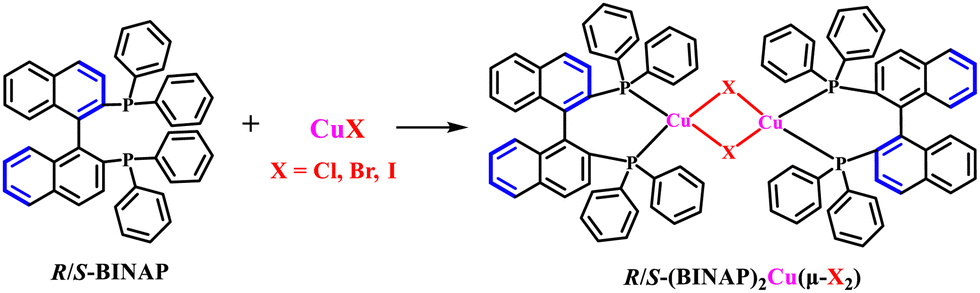 | ||
| Scheme 1 The synthesis procedure and molecular structures of R/S-(BINAP)2Cu(μ-X2) (X = Cl, Br and I) dimers. | ||
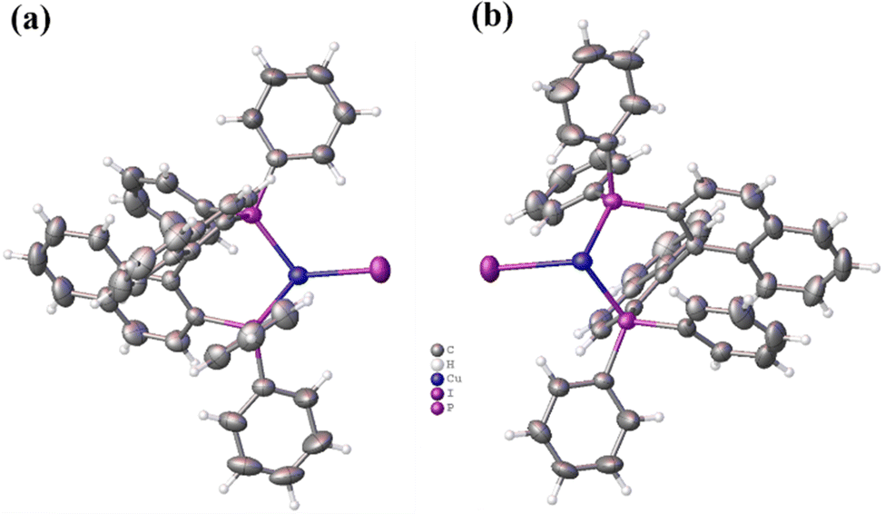 | ||
| Fig. 1 Single crystal structures of (a) R-(BINAP)2Cu(μ-I2) (CCDC: 2215615†) and (b) S-(BINAP)2Cu(μ-I2) (CCDC: 2068898†). | ||
S-(BINAP)2Cu(μ-Cl2), yield: 96.4%. 1H NMR (400 MHz, CDCl3) δ 8.04 (d, J = 6.5 Hz, 2H), 7.40 (d, J = 8.1 Hz, 1H), 7.36 (d, J = 8.7 Hz, 1H), 7.20 (p, J = 6.7, 6.0 Hz, 9H), 7.10 (dt, J = 8.8, 4.5 Hz, 1H), 6.99 (ddd, J = 8.3, 6.7, 1.3 Hz, 1H), 6.79 (d, J = 8.6 Hz, 1H), 6.57 (t, J = 7.5 Hz, 1H), 6.41 (t, J = 7.5 Hz, 2H).
S-(BINAP)2Cu(μ-Br2), yield: 95.8%. 1H NMR (400 MHz, CDCl3) δ 8.08 (q, J = 5.9 Hz, 2H), 7.44–7.38 (m, 1H), 7.35 (d, J = 8.7 Hz, 1H), 7.22 (d, J = 3.6 Hz, 3H), 7.20 (s, 4H), 7.18 (d, J = 5.0 Hz, 2H), 7.12 (dt, J = 8.8, 4.5 Hz, 1H), 6.99 (ddd, J = 8.3, 6.8, 1.3 Hz, 1H), 6.80 (d, J = 8.6 Hz, 1H), 6.56 (t, J = 7.5 Hz, 1H), 6.40 (t, J = 7.6 Hz, 2H).
S-(BINAP)2Cu(μ-I2), yield: 95.2%. 1H NMR (400 MHz, CDCl3) δ 8.17 (qd, J = 5.5, 2.8 Hz, 2H), 7.51–7.40 (m, 2H), 7.35–7.21 (m, 8H), 7.05 (ddd, J = 8.3, 6.7, 1.3 Hz, 1H), 6.86 (d, J = 8.6 Hz, 1H), 6.66–6.58 (m, 1H), 6.46 (t, J = 7.5 Hz, 2H). 13C NMR (101 MHz, CDCl3) δ 137.81, 137.73, 137.65, 134.89, 134.80, 134.71, 132.55, 132.47, 132.38, 132.25, 132.22, 132.18, 131.79, 131.66, 131.54, 131.42, 131.14, 130.95, 130.76, 129.27, 128.59, 128.44, 128.30, 127.75, 127.70, 127.65, 127.55, 127.30, 127.27, 127.23, 127.00, 126.95, 126.91, 126.84, 126.41, 125.88, 125.83, 125.78, 125.16, 124.88.
From the single crystal structures in Fig. 1 and Fig. S7 (ESI†), it can be found that all S-(BINAP)2Cu(μ-Cl2), S-(BINAP)2Cu(μ-Br2) and R/S-(BINAP)2Cu(μ-I2) compounds are dimers consisting of two identical Cu(I) ions, two BINAP ligands and two halide bridges. The dimer-like structures vary with the halogen atoms with bond lengths of Cu–X in the order of Cu–Cl (2.38 Å) < Cu–Br (2.50 Å) < Cu–I (2.69 Å). And the distances between two Cu coordinate centers are 3.09, 3.17 and 3.29 Å for S-(BINAP)2Cu(μ-Cl2), S-(BINAP)2Cu(μ-Br2) and S-(BINAP)2Cu(μ-I2), respectively. Two Cu(I) centers and halide bridges form the off-plane quadrangle with X–Cu–X angle also in the order of Cl–Cu–Cl (98.04°) < Br–Cu–Br (99.91°) < I–Cu–I (100.70°). Accordingly, the angles of the naphthalene rings of the BINAP units are also different with the sequence of I–Cu–I (107.76°) > Br–Cu–Br (72.12°) > Cl–Cu–Cl (71.17°) because the ionic radius of I− (2.16 Å) is bigger than those of Cl− (1.81 Å) and Br− (1.96 Å). These results suggest that the coordinated I− ions have a little greater effect on the structure of R/S-(BINAP)2Cu(μ-I2) than those of R/S-(BINAP)2Cu(μ-Cl2) and R/S-(BINAP)2Cu(μ-Br2). Furthermore, the crystals of R/S-(BINAP)2Cu(μ-I2) demonstrated that they are a mirror image of each other, proving that they are chiral enantiomers. In addition, all dimers show excellent thermal stability, and the thermogravimetric analysis curves indicate that S-(BINAP)2Cu(μ-Cl2), S-(BINAP)2Cu(μ-Br2) and S-(BINAP)2Cu(μ-I2) have high decomposition temperatures (Td, 5% weight-loss) of 395, 392 and 378 °C, respectively, under a nitrogen atmosphere (Fig. S8, ESI†), providing suitable prerequisites for the fabrication of OLEDs.
Photophysical properties
The normalized UV-vis absorption and photoluminescence spectra of S-(BINAP)2Cu(μ-Cl2), S-(BINAP)2Cu(μ-Br2) and S-(BINAP)2Cu(μ-I2) dimers recorded in CH2Cl2 at room temperature and at 77 K in the powder form and doped films are shown in Fig. 2. All compounds showed similar spectra due to the minor differences of Cl−, Br− and I− ions. From the absorption spectra (Fig. 2(a)), it can be found that all dimers show strong absorption bands before 350 nm, which belong to the π–π* absorption of the BINAP ligand. Between 350 and 430 nm, there are also obvious absorption bands, which may be due to the metal ligand charge transfer (MLCT). From the 3D emission maps, it can be observed that the maximum excitation and emission bands are similar at room temperature (Fig. 2(b)), suggesting that these compounds have similar photophysical properties.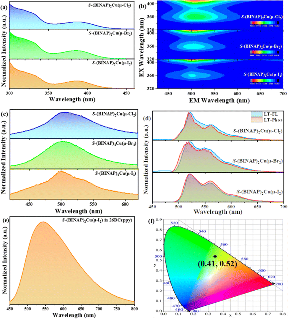 | ||
| Fig. 2 Photophysical characteristics of S-(BINAP)2Cu(μ-Cl2), S-(BINAP)2Cu(μ-Br2) and S-(BINAP)2Cu(μ-I2) dimers: (a) UV-vis absorption, (b) 3D maps and (c) emission spectra in CH2Cl2 (1 × 10⁻⁵ mol L−1) at room temperature; (d) fluorescence and phosphorescence spectra at 77 K in CH2Cl2 (1 × 10⁻⁵ mol L−1); (e) emission spectrum and (f) CIE coordinates of the S-(BINAP)2Cu(μ-I2) doped film in 2,6DCzppy. | ||
All dimers showed that broad emissions cover the broad range of 400–600 nm, peaking at 505, 502 and 500 nm for S-(BINAP)2Cu(μ-Cl2), S-(BINAP)2Cu(μ-Br2) and S-(BINAP)2Cu(μ-I2) dimers, respectively (Fig. 2(c)). But it should be pointed out that all these dimers displayed weak emissions in solution, even hard to be detected by eye under UV-vis lamp excitation. However, the fluorescence and phosphorescence intensities of all materials at 77 K increase greatly (Fig. 2(d)). In addition, the low temperature emission spectra divided three obvious peaks at around 520, 560 and 610 nm for all dimers. Furthermore, the fluorescence and phosphorescence spectra at low temperatures are very close, suggesting that they have close S1/T1 state energies and small S1–T1 energy gaps (ΔEST). The ΔEST values were calculated to be as low as 0.015, 0.019 and 0.004 eV for S-(BINAP)2Cu(μ-Cl2), S-(BINAP)2Cu(μ-Br2) and S-(BINAP)2Cu(μ-I2) dimers, respectively.
Because the S-(BINAP)2Cu(μ-I2) compound was chosen as the dopant in this study, the PL properties of the doped film in the bipolar host material 2,6DCzppy (2,6-bis(3-(9H-carbazol-9-yl)phenyl)pyridine) were also measured (Fig. 2(e)) to modulate the emissive layer of the OLEDs. The emission spectrum is similar to that in CH2Cl2 peaking at 543 nm, but with a much higher intensity with a photoluminescence quantum efficiency (PLQY) of 36.85%. In addition, the spectrum showed a broad full width at half maximum (FWHM) of 148 nm with Commission Internationale de l’ Eclairage coordinates of (0.41, 0.52), belonging to the yellow–green region (Fig. 2(f)). Furthermore, the doped film showed a long-lived PL delayed lifetime of 142 μs at 280 K (Fig. S9, ESI†). With the decrease of temperature, the delayed lifetime becomes longer, and with the increase of temperature, the increased components of delayed fluorescence were also observed (Fig. S10, ESI†), confirming the TADF nature of (BINAP)2Cu(μ-I2).
Chiroptical properties
Because three dimers have similar molecular structures and photophysical properties, the R/S-(BINAP)2Cu(μ-I2) enantiomers were selected as examples to investigate the chiroptical properties including circular dichroism (CD) and CPL spectra in the doped 2,6DCzppy films, which are similar to the reference results.44As illustrated in Fig. 3(a) and (b), the R/S-(BINAP)2Cu(μ-I2) enantiomers showed perfect mirror imaged CD spectra with clear positive and negative Cotton effects at 237, 264, 291, 342 and 382 nm, respectively. The gCD factor–wavelength curves also displayed corresponding shapes with the CD spectra, and the maximum gCD factors reached ±1 × 10⁻² around 347 nm and ±2 × 10⁻² around 394 nm, respectively. But the gCD factors are much smaller (±2 × 10⁻³) at the strong absorption bands before 320 nm. This phenomenon can be explained by the equation of gCD = ICD/(Iabs·32980) (ICD and Iabs represent the absorption intensities of CD and absorption spectra, respectively), and the strong absorption intensities before 340 nm resulted smaller gCD factors.
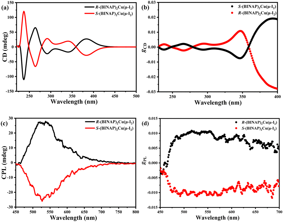 | ||
| Fig. 3 (a) CD spectra and (b) gPLversus wavelength curves, (c) CPL spectra and (d) gPLversus wavelength curves of the R/S-(BINAP)2Cu(μ-I2) doped films in 2,6DCzppy. | ||
Similarly, the CPL spectra in Fig. 3(c) and (d) are also mirror symmetrical to each other with the highest intensity at the maximum peak of the PL spectra. Furthermore, the chirality of the dimers is induced by the R/S-BINAP ligands, but the resulted chiral Cu(I) enantiomers increased the CPL intensity. Therefore, the |gPL| factors of the doped films are over 1 × 10⁻², which are higher than those of the R/S-BINAP ligands and most chiral small molecules.1–15,22–38
Theoretical calculations and electrochemical properties
Density functional theory (DFT) calculations employing the Gaussian09 software with the B3LYP functional were conducted to gain an insight into the frontier molecular orbital distribution and the corresponding composition of each fragment of (BINAP)2Cu(μ-I2). As shown in Fig. 4, the electron cloud is well separated with the highest occupied molecular orbital (HOMO) and the lowest unoccupied molecular orbital (LUMO) on Cu–I and BINAP units. The LUMOs mostly locate on the naphthalene ring of the BINAP ligand (85.813%) with sparse distributions on Cu (1.577%), I (0.430%) and P (4.816%) atoms, respectively. But the HOMOs are composed of the Cu (35.052%), I (31.833%) and P (31.343%) atoms averagely, while only 6.753% disperses on the naphthalene ring. Furthermore, there is only a partial HOMO and LUMO electron cloud overlap, which accords with the characteristics of the TADF material. Both LUMOs and HOMOs have remarkable distribution on the chiral BINAP ligands; that is why the R/S-(BINAP)2Cu(μ-I2) enantiomers have large g factors in the film state.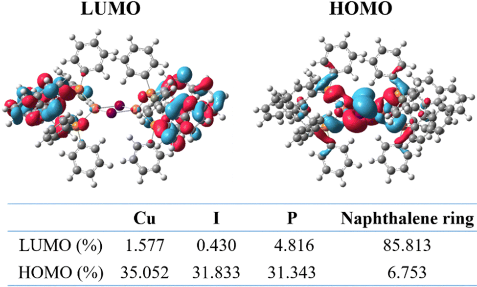 | ||
| Fig. 4 DFT calculations of the HOMO/LUMO distributions and composition of each fragment at the B3LYP/def2-SVP level for (BINAP)2Cu(μ-I2). | ||
Experimentally, the HOMO level was obtained via the oxidation potential, and the LUMO level was calculated from the HOMO level and the band gap (Eg) observed from the UV-vis absorption spectrum. During the progress of anodic oxidation, an obvious oxide peak was observed for S-(BINAP)2Cu(μ-I2) with a potential at 1.05 V (Fig. S11, ESI†), which can be ascribed to the metal-centered Cu(I)/Cu(II) oxide couple. Based on the cyclic voltammetry curve, the HOMO energy level of S-(BINAP)2Cu(μ-I2) was estimated to be -5.51 eV with an equation of EHOMO = −[Eox − E(Fc/Fc+) + 4.8] eV, and the Eg of 2.88 eV was determined from the onset of its UV-vis absorption spectrum (Fig. 2(a)). Based on these data, the LUMO energy level was calculated as −2.63 eV with the equation of ELUMO = EHOMO + Eg.
Electroluminescence properties
Due to the good photophysical and chiroptical properties of the R/S-(BINAP)2Cu(μ-I2) films, they were used as emitters to evaluate the EL and CPEL performances. The doped OLEDs (R/S-D) with an optimized device configuration of indium tin oxide (ITO)/MoO3 (molybdenum oxide, 10 nm)/TAPC (di-(4-(N,N-ditolyl-amino)-phenyl)cyclohexane, 40 nm)/2,6DCzppy: 5 wt% R/S-(BINAP)2Cu(μ-I2) (20 nm)/TmPyPB (1,3,5-tri(m-pyrid-3-ylphenyl)benzene, 50 nm)/LiF (1 nm)/Al (100 nm) were fabricated via the vacuum evaporation method, where MoO3, TAPC, TmPyPB and LiF were adopted as the hole injecting, hole transporting, electron transporting and electron injecting layers, respectively. 2,6DCzppy contains nearly equal electron mobility and hole mobility values of 1 × 10⁻⁵ and 8 × 10⁻⁵ cm2/V·s under an electric field between 6.0 × 10⁵ and 1.0 × 10⁶ V cm−1, which benefit the electron–hole balance in the emissive layer.46 The correlative energy level diagram, the molecular structures of materials used and the relevant EL characteristics are shown in Fig. 5, and the device parameters are summarized in Table 1.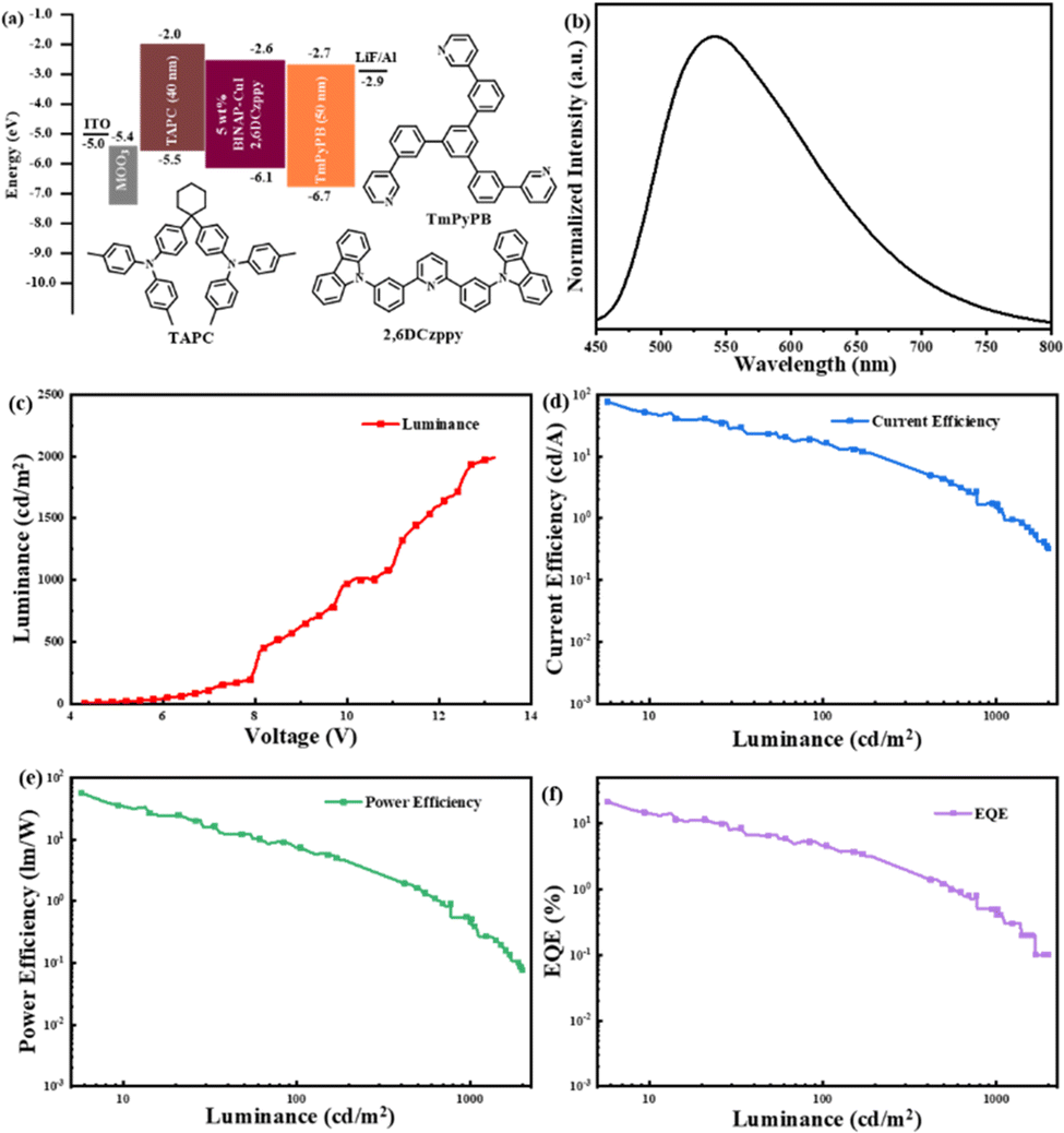 | ||
| Fig. 5 Characteristics of OLEDs: (a) Energy level diagrams and molecular structures of the materials used. (b) Normalized EL spectrum. (c) Luminance–voltage, (d) current density–luminance, (e) power efficiency–luminance and (f) external quantum efficiency–luminance curves. | ||
| Device | V on (V) | λ EL (nm) | L max (cd m−2) | η c,max (cd A−1) | η p,max (lm W−1) | EQEmaxf (%) | CIEg (x, y) | |gEL|h (10−3) |
|---|---|---|---|---|---|---|---|---|
| a Turn-on voltage at 1 cd m−2. b The electroluminescence peak. c Maximum luminance. d Maximum current efficiency. e Maximum power efficiency. f Maximum external quantum efficiency. g CIE coordinates. h |gEL| factor around the EL emission maxima. | ||||||||
| R/S-D | 4.1 | 542 | 1990 | 78 | 57 | 21.7 | (0.34, 0.53) | 3.0 |
The OLED was turned on at a driving voltage of 4.1 V, and the EL spectrum peak is around 542 nm, similar with the PL spectra in the CH2Cl2 solution and the doped film, suggesting that it originates from the R/S-(BINAP)2Cu(μ-I2) dimers. But the CIE coordinates move from (0.41, 0.52) of the PL spectra to (0.34, 0.53) (Fig. S12, ESI†) because of a little narrowed EL spectrum with a FWHM of 136 nm. Furthermore, the OLED showed good performances among the circularly polarised devices. Though the maximum luminance (Lmax) is only about 1990 cd m−2, the maximum current efficiency (ηc,max), power efficiency (ηp,max) and external quantum efficiency (EQEmax) reached 78 cd A−1, 57 lm W−1 and 21.7%, respectively. The device performances are lower than those based on chiral MR-TADF materials, but can be comparable with those of the traditional chiral TADF emitters. We conclude that the poor device performances are due to the relatively low PLQY of 36.85% and a long-lived PL delayed lifetime of 142 μs for the (BINAP)2Cu(μ-I2) emitter. The long-lived delayed lifetime always result in serious nonradiative emission and triplet–triplet annihilation (TTA) and triplet–polaron annihilation (TPA). But due to the vacuum evaporation method used in the device fabrication with a carrier balanced structure and a doped emissive layer, the device performances are much better than those of the reference with the same emitter.44
Subsequently, the CPEL characteristics of the CP-OLEDs based on R/S-(BINAP)2Cu(μ-I2) enantiomers were also investigated. As shown in Fig. 6, obvious CPEL spectra were observed with |gEL| factors in the range of 2× 10⁻³ to 4 × 10⁻³ for (R/S)-D devices during the whole emission region. And, around their EL emission maxima, the |gEL| factors reached 3.0 × 10⁻³, which are higher than those of most CP-OLEDs based on chiral organic TADF materials. But unfortunately, the CPEL spectra and gEL–wavelength curves of the CP-OLEDs are not perfect mirror imaged as the enantiomers. Furthermore, the CPEL intensity and |gEL| factors are also much smaller than the CPL and |gPL| in doped films. Compared with the CPL measurement from the solutions and films, CPEL and gEL detected from the CP-OLEDs are more complicated because the light must pass through the host material, hole transport layer and anode. All the materials can weaken the signal, and inhomogeneous layers also affect the mirror imaged CPEL spectra and gEL curves. Furthermore, according to the hypothesis of Bari et. al.20,21 and the results from our previous work,47 it can be inferred that the spiral direction of CPEL would reverse after the reflection from the cathode, which would also weaken the degree of circular polarization.
 | ||
| Fig. 6 CPEL properties of (R/S)-D: (a) CPEL spectra and (b) gEL–wavelength curves. | ||
Conclusions
In summary, based on R/S-2,2′-bis(diphenylphosphino)-1,1′-binaphthalene (R/S-BINAP) ligands, three chiral copper(I) dimers R/S-(BINAP)2Cu(μ-Cl2), R/S-(BINAP)2Cu(μ-Br2) and R/S-(BINAP)2Cu(μ-I2) were prepared at room temperature with high yields of above 95% in 10 min. The dimers in the solid state and doped films display strong luminescence. Furthermore, R/S-(BINAP)2Cu(μ-I2) enantiomers in doped films also show strong mirror symmetrical CPL spectra with a high |gPL| factor of above 1 × 10⁻². Meanwhile, the evaporated CP-OLEDs based on R/S-(BINAP)2Cu(μ-I2) enantiomers exhibited a high EQE of 21.7%. Notably, the devices also showed mirror imaged CPEL spectra with a |gEL| factor of around 3.0 × 10⁻³. This is a pioneering work on CP-OLEDs based on chiral Cu(I) dimers, and it is possible to improve the device efficiency and g factor by introducing other chiral ligands such as helical structures or optimizing the device structure.Conflicts of interest
The authors declare no conflicts of interest.Acknowledgements
This work was supported by the Fundamental Research Funds for the Central Universities (020514380281).Notes and references
- J. Kumar, T. Nakashima and T. Kawai, J. Phys. Chem. Lett., 2015, 6, 3445–3452 CrossRef CAS.
- J. R. Brandt, F. Salerno and M. J. Fuchter, Nat. Rev. Chem., 2017, 1, 0045 CrossRef CAS.
- J. Han, S. Guo, H. Lu, S. Liu, Q. Zhao and W. Huang, Adv. Opt. Mater., 2018, 6, 1800538 CrossRef.
- D.-W. Zhang, M. Li and C.-F. Chen, Chem. Soc. Rev., 2020, 49, 1331–1343 RSC.
- L. Zhou, G. Xie, F. Ni and C. Yang, Appl. Phys. Lett., 2020, 117, 130502 CrossRef CAS.
- L. Frédéric, A. Desmarchelier, L. Favereau and G. Pieters, Adv. Funct. Mater., 2021, 31, 2010281 CrossRef.
- Z.-L. Gong, X. Zhu, Z. Zhou, S.-W. Zhang, D. Yang, B. Zhao, Y.-P. Zhang, J. Deng, Y. Cheng, Y.-X. Zheng, S.-Q. Zang, H. Kuang, P. Duan, M. Yuan, C.-F. Chen, Y. S. Zhao, Y.-W. Zhong, B. Z. Tang and M. Liu, Sci. China: Chem., 2021, 64, 2060–2104 CrossRef CAS.
- D.-M. Lee, J.-W. Song, Y.-J. Lee, C.-J. Yu and J.-H. Kim, Adv. Mater., 2017, 29, 1700907 CrossRef.
- M. Shimada, Y. Yamanoi, T. Ohto, S. T. Pham, R. Yamada, H. Tada, K. Omoto, S. Tashiro, M. Shionoya, M. Hattori, K. Jimura, S. Hayashi, H. Koike, M. Iwamura, K. Nozaki and H. Nishihara, J. Am. Chem. Soc., 2017, 139, 11214–11221 CrossRef CAS PubMed.
- E. Spuling, N. Sharma, I. D. W. Samuel, E. Zysman-Colman and S. Brase, Chem. Commun., 2018, 54, 9278–9281 RSC.
- S. Y. Yang, Y. K. Wang, C. C. Peng, Z. G. Wu, S. Yuan, Y. J. Yu, H. Li, T. T. Wang, H. C. Li, Y. X. Zheng, Z. Q. Jiang and L. S. Liao, J. Am. Chem. Soc., 2020, 142, 17756–17765 CrossRef CAS PubMed.
- Z.-L. Tu, Z.-P. Yan, X. Liang, L. Chen, Z.-G. Wu, Y. Wang, Y.-X. Zheng, J.-L. Zuo and Y. Pan, Adv. Sci., 2020, 7, 2000804 CrossRef CAS PubMed.
- Y.-P. Zhang, X. Liang, X.-F. Luo, S.-Q. Song, S. Li, Y. Wang, Z.-P. Mao, W.-Y. Xu, Y.-X. Zheng, J.-L. Zuo and Y. Pan, Angew. Chem., Int. Ed., 2021, 60, 8435–8440 CrossRef CAS PubMed.
- X. Wu, J.-W. Huang, B.-K. Su, S. Wang, L. Yuan, W.-Q. Zheng, H. Zhang, Y.-X. Zheng, W. Zhu and P.-T. Chou, Adv. Mater., 2022, 34, 2105080 CrossRef CAS PubMed.
- Y.-P. Zhang, M.-X. Mao, S.-Q. Song, Y. Wang, Y.-X. Zheng, J.-L. Zuo and Y. Pan, Angew. Chem., Int. Ed., 2022, 61, e202200290 CAS.
- T. Imagawa, S. Hirata, K. Totani, T. Watanabe and M. Vacha, Chem. Commun., 2015, 51, 13268–13271 RSC.
- F. Song, Z. Xu, Q. Zhang, Z. Zhao, H. Zhang, W. Zhao, Z. Qiu, C. Qi, H. Zhang, H. H. Y. Sung, I. D. Williams, J. W. Y. Lam, Z. Zhao, A. Qin, D. Ma and B. Z. Tang, Adv. Funct. Mater., 2018, 28, 1800051 CrossRef.
- E. Peeters, M. P. T. Christiaans, R. A. J. Janssen, H. F. M. Schoo, H. P. J. M. Dekkers and E. W. Meijer, J. Am. Chem. Soc., 1997, 119, 9909–9910 CrossRef CAS.
- Y. Yang, R. C. da Costa, M. J. Fuchter and A. J. Campbell, Nat. Photonics, 2013, 7, 634–638 CrossRef CAS.
- F. Zinna, U. Giovanella and L. Di Bari, Adv. Mater., 2015, 27, 1791–1795 CrossRef CAS PubMed.
- F. Zinna, M. Pasini, F. Galeotti, C. Botta, L. Di Bari and U. Giovanella, Adv. Funct. Mater., 2017, 27, 1603719 CrossRef.
- T.-Y. Li, Y.-M. Jing, X. Liu, Y. Zhao, L. Shi, Z. Tang, Y.-X. Zheng and J.-L. Zuo, Sci. Rep., 2015, 5, 14912 CrossRef CAS PubMed.
- J. R. Brandt, X. Wang, Y. Yang, A. J. Campbell and M. J. Fuchter, J. Am. Chem. Soc., 2016, 138, 9743–9746 CrossRef CAS PubMed.
- D. Di Nuzzo, C. Kulkarni, B. Zhao, E. Smolinsky, F. Tassinari, S. C. J. Meskers, R. Naaman, E. W. Meijer and R. H. Friend, ACS Nano, 2017, 11, 12713–12722 CrossRef CAS.
- D. M. Lee, J. W. Song, Y. J. Lee, C. J. Yu and J. H. Kim, Adv. Mater., 2017, 29, 1700907 CrossRef PubMed.
- L. Wan, J. Wade, F. Salerno, O. Arteaga, B. Laidlaw, X. Wang, T. Penfold, M. J. Fuchter and A. J. Campbell, ACS Nano, 2019, 13, 8099–8105 CrossRef CAS.
- S. Feuillastre, M. Pauton, L. Gao, A. Desmarchelier, A. J. Riives, D. Prim, D. Tondelier, B. Geffroy, G. Muller, G. Clavier and G. Pieters, J. Am. Chem. Soc., 2016, 138, 3990–3993 CrossRef CAS PubMed.
- M. Li, S. H. Li, D. Zhang, M. Cai, L. Duan, M. K. Fung and C. F. Chen, Angew. Chem., Int. Ed., 2018, 57, 2889–2893 CrossRef CAS PubMed.
- Z.-G. Wu, H.-B. Han, Z.-P. Yan, X.-F. Luo, Y. Wang, Y.-X. Zheng, J.-L. Zuo and Y. Pan, Adv. Mater., 2019, 31, 1900524 CrossRef.
- S. Sun, J. Wang, L. Chen, R. Chen, J. Jin, C. Chen, S. Chen, G. Xie, C. Zheng and W. Huang, J. Mater. Chem. C, 2019, 7, 14511–14516 RSC.
- N. Sharma, E. Spuling, C. M. Mattern, W. Li, O. Fuhr, Y. Tsuchiya, C. Adachi, S. Brase, I. D. W. Samuel and E. Zysman-Colman, Chem. Sci., 2019, 10, 6689–6696 RSC.
- L. Frédéric, A. Desmarchelier, R. Plais, L. Lavnevich, G. Muller, C. Villafuerte, G. Clavier, E. Quesnel, B. Racine, S. Meunier-Della-Gatta, J. P. Dognon, P. Thuéry, J. Crassous, L. Favereau and G. Pieters, Adv. Funct. Mater., 2020, 30, 2004838 CrossRef.
- M. Li, Y. F. Wang, D. Zhang, L. Duan and C. F. Chen, Angew. Chem., Int. Ed., 2020, 59, 3500–3504 CrossRef CAS PubMed.
- F. Ni, C.-W. Huang, Y. Tang, Z. Chen, Y. Wu, S. Xia, X. Cao, J.-H. Hsu, W.-K. Lee, K. Zheng, Z. Huang, C.-C. Wu and C. Yang, Mater. Horiz., 2021, 8, 547–555 RSC.
- L. Frédéric, A. Desmarchelier, L. Favereau and G. Pieters, Adv. Funct. Mater., 2021, 31, 2010281 CrossRef.
- L. Zhang, I. Song, J. Ahn, M. Han, M. Linares, M. Surin, H. J. Zhang, J. H. Oh and J. Lin, Nat. Commun., 2021, 12, 142 CrossRef CAS PubMed.
- J.-R. Jiménez, M. Poncet, S. Míguez-Lago, S. Grass, J. Lacour, C. Besnard, J. M. Cuerva, A. G. Campaña and C. Piguet, Angew. Chem., Int. Ed., 2021, 60, 10095–10102 CrossRef.
- Z.-P. Yan, L. Yuan, Y. Zhang, M.-X. Mao, X.-J. Liao, H.-X. Ni, Z.-H. Wang, Z. An, Y.-X. Zheng and J.-L. Zuo, Adv. Mater., 2022, 34, 2204253 CrossRef CAS PubMed.
- N. Berova, K. Nakanishi and R. Woody, Circular Dichroism, Principles and Applications, Wiley- VCH, New York, 2nd edn, 2000 Search PubMed.
- J. A. Schellman, Chem. Rev., 1975, 75, 323–331 CrossRef CAS.
- B. Doistau, J.-R. Jiménez and C. Piguet, Front. Chem., 2020, 8, 555 CrossRef CAS.
- F. Zinna, T. Bruhn, C. A. Guido, J. Ahrens, M. Bröring, L. Di Bari and G. Pescitelli, Chem. – Eur. J., 2016, 22, 16089–16098 CrossRef CAS.
- F. Zinna, L. Arrico, T. Funaioli, L. Di Bari, M. Pasini, C. Botta and U. Giovanella, J. Mater. Chem. C, 2022, 10, 463–468 RSC.
- J.-J. Wang, H.-T. Zhou, J.-N. Yang, L.-Z. Feng, J.-S. Yao, K.-H. Song, M.-M. Zhou, S. Jin, G. Zhang and H.-B. Yao, J. Am. Chem. Soc., 2021, 143, 10860–10864 CrossRef CAS.
- X. Liang, X.-F. Luo, Z.-P. Yan, Y.-X. Zheng and J.-L. Zuo, Angew. Chem., Int. Ed., 2021, 60, 24437–24442 CrossRef CAS.
- S.-J. Su, C. Cai and J. Kido, Chem. Mater., 2011, 23, 274–284 CrossRef CAS.
- Z.-P. Yan, X.-F. Luo, W.-Q. Liu, Z.-G. Wu, X. Liang, K. Liao, Y.-X. Zheng, L. Zhou, J.-L. Zuo, Y. Pan and H. Zhang, Chem. – Eur. J., 2019, 25, 5672–5676 CrossRef CAS.
Footnote |
| † Electronic supplementary information (ESI) available. CCDC 2068678, 2068899, 2215615 and 2068898. For ESI and crystallographic data in CIF or other electronic format see DOI: https://doi.org/10.1039/d2tc04895g |
| This journal is © The Royal Society of Chemistry 2023 |