
 Open Access Article
 This Open Access Article is licensed under a
 Creative Commons Attribution 3.0 Unported Licence
Optical losses in silicon heterojunction solar cells: analysis of record-efficiency devices and practical limits based on ray-tracing simulations†
Erik M.
Spaans
 *ab,
Selvaraj
Venkataraj
b,
Krishna
Singh
b,
Ashwath
Ravichandran
b,
Maria L.
Manalo
b,
Rosalie
Guerra
b,
Armin G.
Aberle
ab and
Nitin
Nampalli
b
*ab,
Selvaraj
Venkataraj
b,
Krishna
Singh
b,
Ashwath
Ravichandran
b,
Maria L.
Manalo
b,
Rosalie
Guerra
b,
Armin G.
Aberle
ab and
Nitin
Nampalli
b
aDepartment of Electrical and Computer Engineering, National University of Singapore, Singapore 117583, Singapore. E-mail: erik.spaans@u.nus.edu
bSolar Energy Research Institute of Singapore, National University of Singapore, Singapore 117574, Singapore
First published on 28th March 2025
Abstract
The efficiency of record silicon heterojunction (SHJ) solar cells for both front-and-back contacted (FBC) and interdigitated back-contacted (IBC) architectures has improved significantly in recent years. This is largely due to considerable improvements in short-circuit current density (Jsc) driven by recent industrial innovations resulting in highly transparent layers and novel metallisation. In this work we present the first detailed, side-by-side Jsc loss comparison of recent record solar cells enabled by a carefully calibrated and thoroughly validated optical ray-tracing model and derive a practically achievable Jsc limit for modern FBC-SHJ and IBC-SHJ solar cells for different silicon wafer thicknesses. By modelling recent SHJ record-efficiency cells based on published data, we obtain spectrally resolved Jsc losses and estimated complex refractive indices for all functional layers used in record SHJ solar cells as of 2024 from Hanergy, Maxwell, SunDrive, LONGi, Panasonic and Kaneka. Pathways for further improvement in Jsc are also described.
Broader contextSilicon heterojunction (SHJ) solar cells have dominated silicon record efficiencies since 2014. More recently, there has been a significant increase in the number of high-efficiency SHJ solar cells reported, largely enabled by improvements in the device short-circuit current density (Jsc). With a recent world-wide surge in the manufacturing capacity of SHJ solar cells, it is imperative to understand the developments that are necessary to reach high device Jsc and the potential opportunities that lie ahead. With the help of ray-tracing optical models, Jsc loss distributions of recent record SHJ solar cells are unravelled and potential improvements are evaluated to quantify practical Jsc limits for both device contacting architectures: front-and-back contacted (FBC) and interdigitated back-contacted (IBC). The insights derived in this work provide a useful technology roadmap for the continued enhancement of the optical performance of record-efficiency and industrial SHJ solar cells. |
1. Introduction
Over the past 10 years, there has been remarkable progress in the power conversion efficiency (PCE) of silicon heterojunction (SHJ) solar cells. Owing to the excellent surface passivation enabled by intrinsic hydrogenated amorphous silicon [a-Si:H(i)] layers,1 high open-circuit voltages (Voc) were already achieved in 2000.2 The Voc of these devices (∼720 mV) was higher than the then record PCE of 24.7% of a passivated emitter, rear locally-diffused (PERL) structure with a Voc of 706 mV.3 It is clear that SHJ devices primarily underperformed in regard to the fill factor (FF) and the short-circuit current density (Jsc). For the FF, the main losses arise from carrier recombination and resistive losses.4,5 Steady improvements have been made on this front in recent years.6,7 However, a crucial bottleneck to higher efficiency for SHJ devices remained the Jsc, which is limited by optical losses. This is indicated in Fig. 1, which shows a strong correlation between the PCE and Jsc values for a number of recent high-PCE SHJ solar cells, including all record cells of the last 10 years. Here, we distinguish between front-and-back contacted (FBC) and interdigitated back-contacted (IBC) architectures.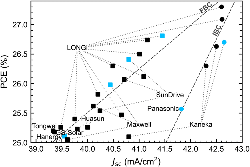 | ||
| Fig. 1 Certified PCEs of commercial FBC (squares) and IBC (circles) SHJ solar cells vs. Jsc.4,7–28 The dashed lines are linear fits to the cells of each architecture. The highlighted points are analysed in this work. | ||
Since the introduction of SHJ-like solar cells in 1992 by Sanyo,29 the record efficiencies for this device architecture have been spearheaded by several solar cell manufacturers. A record PCE of 23.7% (Jsc 39.4 mA cm−2) was reached in 2011 by Kaneka,30 and was improved to 24.7% (Jsc 39.6 mA cm−2) in a FBC structure in 2013 by Panasonic.31 The next jump came a year later with a 25.6%-efficient solar cell (Jsc 41.8 mA cm−2) in an IBC design,15 which is evident in the sharp increase in Jsc. This result was the first time that a SHJ solar cell became the best-performing silicon-based device architecture, as is evident in the NREL Solar cell efficiency chart.10,32 Kaneka followed on a similar path, reaching a FBC efficiency of 25.1% (Jsc 40.8 mA cm−2),4 followed by a world-record efficiency of 26.7% (Jsc 42.7 mA cm−2) with an IBC solar cell in 2017.8 LONGi then followed a similar development path (FBC to IBC) to achieve a 26.8% (Jsc 41.5 mA cm−2) FBC record cell in 2022,9 followed by a 27.3% (Jsc 42.6 mA cm−2) IBC device in 2023.10
Concurrent to these developments, the manufacturing capacity for SHJ solar cells has also increased significantly since 2019, and the SHJ solar cell market share is expected to reach 19% over the next ten years in a TWp-level global production capacity.33 This rapid ramp-up in SHJ cell capacity has generated an increasing need in the PV industry to better understand (1) the drivers of the Jsc loss in industrial SHJ solar cells, (2) the most effective methods to further improve the Jsc of these cells, and (3) the practical upper limit of Jsc achievable in industrial FBC-SHJ and IBC-SHJ cells. Unfortunately, a definitive answer to these questions is not very clear yet.
It is generally understood that high parasitic absorption in the intrinsic, n- and p-doped a-Si:H [a-Si:H(i), a-Si:H(n), a-Si:H(p), respectively] layers and the transparent conductive oxide (TCO, usually in-doped tin oxide or ITO) layer at the front side of the SHJ device is responsible for the low Jsc of SHJ solar cells.34 An additional TCO at the rear of the cell also contributes to an enhanced parasitic absorption in the near-infrared (NIR). Finally, excessive front metal shading as well as rear metal absorption (in the case of monofacial devices) is well known to have detrimental effects on Jsc.35 However, the exact contributions of these various factors to the total Jsc loss of high-efficiency industrial SHJ devices is not yet very clear.
While there have been several recent works on record-efficiency solar cells which have attempted to provide a quantitative breakdown of Jsc losses, the specific contributions to these losses from the various individual functional layers in a SHJ cell is typically not available and is often reported in terms of lumped losses.14,17,21 These lumped losses are estimated from external quantum efficiency (EQE) and reflectance (R) measurements. In the few cases where losses from individual layers were made available (e.g. via ray-tracing simulations), the assumptions, fundamental data and modelling steps used in the simulations were not fully disclosed.6,9 This makes it impossible to compare Jsc loss contributions (and therefore the degree of Jsc improvement) between the different studies. The inability to draw such comparisons also prevents a sound quantitative understanding of Jsc losses in these recent high-Jsc SHJ solar cells.
Several optical improvements were reported for these high-Jsc SHJ solar cells, which partly deviate from the ‘classical’ SHJ structure (i.e. a-Si- and ITO-based layers). Firstly, more transparent a-Si:H(i) layers were used,11,15 which is important to reduce the parasitic absorption at the front. Second, TCOs with higher mobility and transparency than ITO were implemented.9,17 Third, nc-SiOx:H(n), a more transparent window layer, is ubiquitous in recent FBC-SHJ record devices.6,9,17 Finally, a reduction in the front shading fraction has also given a direct boost to record-Jsc FBC-SHJ solar cells.9,17 While the general approaches to improving Jsc are known, it is not very clear what the shortest pathway is to bring the Jsc of industrial SHJ solar cells to the level of the record cells, or what approaches are most promising to further increase the Jsc beyond the current record values.
This also leads to the question of practical Jsc limits in industrial SHJ solar cells. There are several works that attempt to quantify the theoretical upper limit of Jsc in silicon solar cells in general, but a majority of these are derived from first principles and are not specific to SHJ cells.36,37 The number of studies that have attempted to quantify a practical upper limit specifically for SHJ solar cells is limited,21,38,39 and the assumptions underlying the predicted limit are not supported by detailed modelling and only refer to IBC architectures. New developments since the publication of these works could also lead to higher practical cell Jsc values than initially predicted. Therefore, an updated and thoroughly validated practical Jsc limit for SHJ cells in FBC and IBC structures is missing.
This work aims to tackle these questions by providing a side-by-side comparison of the detailed optical losses of several reported high-efficiency SHJ solar cells through carefully calibrated ray-tracing-based optical modelling. After validating the model in Section 2.1 with an in-house fabricated FBC-SHJ solar cell, in Section 2.2 we adopt the device structures from several high-efficiency SHJ solar cells and derive their optical properties based on reported solar cell details and the EQE and R data. The resulting model enables us to quantify the often-unknown distribution of the Jsc losses resulting from parasitic absorption in all the layers of the device, from shading and from escape losses. We also derive important insights from this analysis to (1) clarify the optical requirements needed to achieve record-high Jsc in SHJ solar cells for both FBC and IBC configurations and (2) identify the most effective pathways to improve the Jsc of industrial SHJ cells. In Section 2.3 we use a ray-tracing model to re-evaluate the practical Jsc limits for different wafer thicknesses for both FBC-SHJ and IBC-SHJ solar cells, using reasonable material properties based on the current stage of development as of 2024. This enables a more realistic prediction of the practical Jsc limits under different contacting configurations, which has not been reported before. Finally, Section 3 presents the main conclusions of this work.
2. Results and discussion
2.1. Validated optical models for FBC-SHJ and IBC-SHJ solar cells
The optical response of a SHJ solar cell is a combined effect of the reflection and transmission at interfaces between the various layers as well as absorption within the layers. Several works in the literature rely on device-level measurements (EQE and R) to validate their model.40–43 However, since SHJ solar cells are typically comprised of at least 7 optical layers, relying solely on EQE and R measurements can lead to systematic errors in Jsc loss estimations as such measurements reflect only the cumulative response of the device (i.e. of all 7 or more optical layers combined). This makes it difficult to accurately attribute Jsc losses to specific individual optical layers.To tackle this problem, we utilize optical ray tracing, which is essential to provide a breakdown of losses within each individual layer. We use GenPro4,44 a software that combines wave and ray optics to accurately model thin films on textured surfaces. Furthermore, we do not rely only on a single cell-level dataset (cell EQE and R) to validate the output of the ray-tracing model. Instead, we use a comprehensive dataset obtained from single-layer measurements, measurements on stacked layers, solar cell precursors and measurements on fully-finished FBC solar cells. The development of a validated model for FBC-SHJ and IBC-SHJ solar cells used in this work is described in more detail in the following sections.
 | ||
| Fig. 2 Optical structure for (A) FBC-SHJ and (B) IBC-SHJ solar cells used in this work. A chuck, assumed to be used during EQE measurements, is included. ARC: anti-reflection coating. | ||
In addition to the cell optical structures shown in Fig. 2, additional optical structures were also created that correspond to FBC cell precursors (at various stages of processing) and other test samples with individual layers. Model validation is then performed by comparing the simulated output of optical structures against the measured data from the fabricated samples. Careful characterization steps are performed after different stages of the SHJ fabrication process, similar to our previous work.45 This includes the following key steps:
(1) Wavelength-dependent complex refractive indices (n and k) of all the layers of the device (except for c-Si, for which we use its published refractive index at 25 °C)46 were determined by simultaneous fitting of spectroscopic ellipsometry (SE) and reflectance/transmittance (RT) measurements on planar substrates. For the a-Si-based layers, ∼300 nm of SiOx on a Si wafer was used as planar substrate to enhance the interference effects from the sample and improve the parameter sensitivity in the fitting stage,47 for which a Tauc–Lorentz dispersion model was used.48 For the TCO, an additional Drude oscillator was included in the model to account for free-carrier absorption (FCA),49 and the planar substrate used was glass. This was done to obtain more information from the transmittance measurements. As all these layers were deposited onto a planar substrate, their actual thickness in the final solar cell is expected to be lower, as the actual solar cells have a pyramid-textured surface. To account for this difference, the thicknesses on textured samples are fitted from RT measurements of single layers on a textured wafer, as described in Section 2.1.2.
(2) RT measurements were performed on 4 different test structures corresponding to 4 critical stages of processing: (a) on a bare (i.e., unpassivated) textured wafer, (b) after single-layer depositions of all the layers present the final solar cell stack [a-Si:H(i), a-Si:H(n), a-Si:H(p) and ITO], (c) on multi-layer stacks (a-Si:H(i)/a-Si:H(n), a-Si:H(i)/a-Si:H(p) and solar cell precursor), (d) after metallisation. All sample groups (a)–(d) were subsequently subjected to the same annealing conditions (200 °C for 10 minutes), which is used in-house for curing/contact formation using a pure Ag metallisation paste. Sample groups (a) and (b) are used to fit the optical properties and thicknesses of the individual layers on textured Si, sample group (c) is used only for the verification of modelled properties on multi-layer stacks, and sample group (d) for the final device response.
(3) Finished FBC solar cells were subjected to current–voltage (I–V) measurements as well as spot-EQE and R measurements.
The resulting dataset therefore consists of: (1) RT of thin films, precursors and cells, (2) n and k of individual layers, and (3) EQE and R of metallized FBC cells. By cross-validating these three datasets, an accurate model for FBC-SHJ solar cells was derived (shown in Fig. 2A). Details of these measurements and the validation of the derived FBC optical model can be found in Appendix A, ESI.† The optical model for IBC cells was then obtained by minor modifications of the FBC cell model, as described below. Note that the IBC optical model was not validated with real in-house fabricated cells; however, as described later, the IBC models are confirmed to be sufficiently accurate for deriving quantitative insights into loss mechanisms.
2.1.2.1. Wafer. For the c-Si wafer, the modelled angle of a random pyramid texture was adjusted to match the measured R, keeping the wafer thickness fixed at the measured value in this study of 160 μm. An excellent match was obtained [within 0.02%abs weighted average reflectance (WAR) and minimal spectral mismatch]. The thickness of the deposited thin films (a-Si and TCO layers) on textured silicon used in the cell's optical model was determined by matching the modelled and measured RT data from precursor samples. The resulting thicknesses on textured surfaces were as expected (estimated by applying a texture correction factor of 1.5–1.6 to the thicknesses measured on planar surfaces). This approach ensured that the right thickness is used in the final solar cell model. The weighted average of the modelled RT for all layers were found to be within 0.5%abs of that of the measured data, indicating excellent agreement between the experimental and modelled RT curves.
2.1.2.2. Stacks. To verify the behaviour of individual layers as a stack, we rely on cell precursor samples at different stages of processing (previously described in Section 2.1.1). We measured RT data on physical samples and compared them to the simulated RT of the corresponding stacks using GenPro4.44 The previously determined refractive indices and the thicknesses on textured wafers of each individual layer are used as inputs to the model. The weighted average of all of the modelled RT spectra again showed a low deviation of less than 0.75%abs compared to the measured data for all stacks.
2.1.2.3. Metal contacts. As the optical simulator used is one-dimensional, the effects of partial metal coverage on the front and rear surfaces (for FBC cells) could not be directly modelled. To account for the optical interaction at metal interfaces at the front and rear surfaces, we separately considered 3 cross-sectional areas in a FBC solar cell: (a) areas where only front metal is present, (b) areas where only rear metal is present, and (c) areas where front and rear metal overlap. Areas where neither front nor rear metal is present are equivalent to non-metallized areas of the cell, which have already been taken into account. We then performed a detailed analysis of the impact of metallized areas on solar cell optics, which is provided in Appendix B, ESI.† Based on this analysis, we were able to reliably estimate the impact of metal coverage in FBC solar cells by scaling all the simulation spectra with the non-shaded area fraction of the device and adding a constant loss over the full spectrum to simulate the optical loss from the front metal fingers. Also, as demonstrated in Appendix B, ESI,† areas where only rear metal is present can be ignored for FBC cells as they have only a negligible impact on the device Jsc. In the case of IBC devices [which only contain cross-section type (b) as described above], we were able to simulate the rear to sufficient precision by simply assuming 100% rear metal coverage. All the simulations in this work are post-processed in this same way to account for metallisation effects.
2.1.2.4. Measurement setup. The angle between the plane perpendicular to the samples and the incident light beam used for all R measurements was 8° in the specific measurement setup used in this study, which is fairly common for integrating sphere setups. Hence, simulations for all simulated R spectra were also conducted with the same angle of incidence. For RT measurements of single layers and cell precursors, no chuck at the rear of the stack is assumed. For cell EQE and R measurements, a rear stack of air/metal is added to the model to simulate the presence of the measurement chuck (similar to the conditions during these measurements). To ensure that we closely match the R of the contacting chuck used in our in-house measurements, its refractive index was determined experimentally from R measurements (see Appendix A, ESI,† for details).
2.1.2.5. Collection efficiency. To derive the solar cell Jsc from optical absorption spectra, the carrier collection efficiency (CE) was defined for each layer. A CE of 100% is assumed for the c-Si.34 For other layers, the layer thicknesses and their refractive indices were previously validated, and the CE was obtained by comparing the EQE data with the modelled absorption profile of the c-Si wafer. This comparison showed that the absorption from the front-side layers is not purely parasitic but also contributes to electrical output. Hence, following the work by Holman et al.,34 we assumed a non-zero CE for the front a-Si:H(i). A CE of 32% was found to fit the spot-EQE measurements the best, which is very close to the values estimated in other works.34,43 A good match between the measured and simulated spot-EQE (0.01 mA cm−2Jsc difference) and spot-R (−0.19 mA cm−2Jsc difference) is evident in Fig. 3, which shows minimal spectral mismatch between simulated and measured EQE and R data.
 | ||
| Fig. 3 Simulated and measured spot-EQE and spot-R for our reference in-house FBC-SHJ solar cell. | ||
This concludes the procedure used to validate the FBC-SHJ solar cell optical model. For IBC-SHJ cells, we were not able to validate the corresponding model shown in Fig. 2B using real devices since IBC-SHJ solar cells could not be fabricated in-house at the time of this study. Nevertheless, the same layers that were validated for FBC cells are also used in the IBC model, hence we also expect the IBC-SHJ model to have a high accuracy. This is later confirmed in the following section, where both the FBC and IBC models are applied to reported data from other record-efficiency solar cells and shown to produce comparably low levels of spectral mismatch.
It was found that the few previous studies on SHJ solar cell modelling only use a subset of these methodologies to model the optical behaviour of fabricated SHJ solar cells.6,9,40–43 Even though some of them are able to achieve low levels of mismatch with measured EQE and R data, the detailed layer fitting and verification steps used in the present work enhance the model confidence well beyond what was achieved in previous works.
2.2. J sc loss analysis of record SHJ solar cells
The validated model for an in-house FBC-SHJ solar cell developed in Section 2.1 can now be used as a starting point to estimate spectral Jsc losses for certified record devices from the past 10 years for which enough device information is available to create a reliable model. These are the highlighted points in Fig. 1. In all of these cases, no detailed spectral losses in the different layers were reported. Hence, the application of the FBC-SHJ and IBC-SHJ models developed in this work allows, for the first time, (1) a detailed breakdown of estimated optical losses for 6 record solar cells and (2) an ‘apple-to-apple’ comparison of optical losses between multiple record solar cells. In order to do this, the in-house model described in Section 2.1 had to be customized for each reported record solar cell. The assumptions and nature of model customization are described in Section 2.2.1. Details of the final model for each of these cells, along with the quality of fit between the measured and simulated cell EQE is described in Section 2.2.2. In Section 2.2.3, we report on the process developments to reach these high Jsc values, followed by the main improvement pathways for industrial SHJ solar cells in Section 2.2.4 and a discussion in Section 2.2.5 wherein insights from our model are compared with those from other FBC-SHJ modelling efforts in the literature.Next, it was attempted to obtain an estimate of the refractive indices of all the layers in the record devices (except the c-Si wafer). This was done by comparing the degree of match between our simulated EQE and R, and the published EQE and R data from the record devices. In our previous study,45 we found that the layers used in these high-efficiency devices are much more transparent than typical layers for which published data is available in the literature, and we accounted for this superior transparency by scaling the extinction coefficient k with a constant factor while keeping the refractive index n fixed. Despite obtaining accurate fits with this approach, the final n and k of some layers were unlikely to be representative of real materials and could not be fitted with commonly used dispersion laws (e.g. Tauc–Lorentz or other oscillator models) or pass self-consistency checks using the Kramers–Kronig (KK) relationship.55 In the present work, we improve on this methodology by modelling the refractive index of all layers from the record devices exclusively using dispersion laws. As with the measurements of our in-house layers, we used a single Tauc–Lorentz oscillator for the amorphous and nanocrystalline Si thin films, while adding an additional Drude model in the case of the modelled TCOs. Several simulations were performed in which parameters of the oscillator models were varied until a best-fit match was obtained to the reported EQE and R from the record devices. The resulting oscillator parameters and refractive index data for each of the layers were therefore representative of the typical class of materials that we aim to describe with these dispersion laws and were largely self-consistent using the KK relationship. More details on this modelling routine are provided in Appendix C, ESI.†
Using the approach described above, customized models for all record FBC-SHJ cells targeted for comparison in this work could be successfully created. As shown in Fig. 4, all models result in a very low mismatch to the published EQE data of the record cells. The degree of mismatch is discussed in more detail in Section 2.2.2.
 | ||
| Fig. 4 Simulated spectral optical losses of record FBC-SHJ and IBC-SHJ solar cells as modelled in this work, along with the certified EQE data of each device: (A) Hanergy FBC (PCE 25.11%),6 (B) Maxwell FBC (PCE 25.98%),17 (C) SunDrive FBC (PCE 26.41%),17 (D) LONGi FBC (PCE 26.81%),56 (E) Panasonic IBC (PCE 25.57%),15 and (F) Kaneka IBC (PCE 26.7%).57 Note: the modelled solar cells do not have a published spectral loss breakdown. The values in parenthesis in the graphs correspond to the integrated Jsc loss or contribution in mA cm−2. | ||
Typically, the level of mismatch between experimental EQE (EQEref) and simulated EQE (EQEsim) data is determined by the difference in integrated EQE spectra:
 | (1) |
 | (2) |
This figure of merit is spectrally decomposed, meaning that if small values of Δ|Jsc| are obtained, we not only know that the final Jsc value is estimated adequately, but also that the simulated and measured EQE curves have a high degree of spectral match. Fig. 4 shows the best fits to the EQEs of the record SHJ devices, along with the simulated spectra of the parasitic absorption, reflectance and shading as modelled in this work. Note that the two bottom curves in each subplot within Fig. 4 quantify respectively (1) the error in the simulated EQE [EQEe(λ) = EQEsim(λ) − EQEref(λ)] and (2) the corresponding error in terms of Jsc for a spectral interval of 10 nm applied over the AM1.5G spectrum, denoted φAM1.5G10nm(λ) [Jsce(λ) = q EQEe(λ) φAM1.5G10nm(λ)].
It is clear from Fig. 4 that for most of the fitted record EQEs, the usual figure of merit, ΔJsc, is well below 0.03 mA cm−2. This indicates a good overall match to the Jsc between the actual and simulated record device. However, Fig. 4 also shows that the new figure of merit introduced in this work [from eqn (1)], Δ|Jsc|, mostly has values below 0.3 mA cm−2 for all simulated record cells (with only one being 0.45 mA cm−2), which further indicates a high degree of spectral match between the measured and simulated EQE. We note that the spectrally decomposed figure of merit for EQE and Jsc mismatch proposed in eqn (2) in this work (Δ|Jsc|) is unique and has not been used or reported in any of the previous studies on Jsc modelling of SHJ solar cells.
Finally, all the modelling parameters (including the device structure, layer thicknesses, front metal shading fraction and the complex refractive indices) used for each of the record devices are provided in Appendix E, ESI,† while Table 1 summarizes the measured and modelled Jsc and the corresponding fit errors for all the record cells analysed in this work. We note that for some devices, non-trivial differences are observed between the Jsc determined from the certified I–V and EQE measurements, which can be due to differences in full-area/spot measurements, different illumination settings for each measurement or measurement uncertainties. Where such differences exist, we have computed the solar cell Jsc from the integrated EQE curve rather than I–V data as this is more useful for the purposes of this study.
| Type | Name | PCE (%) | J sc values (mA cm−2) | ||||
|---|---|---|---|---|---|---|---|
| Cert. I–V | Cert. EQE | Sim. EQE | ΔJsc | Δ|Jsc| | |||
| FBC | Hanergy | 25.11 | 39.55 | 39.29 | 39.28 | −0.01 | 0.45 |
| Maxwell | 25.98 | 40.44 | 40.44 | 40.47 | 0.03 | 0.22 | |
| SunDrive | 26.41 | 40.80 | 40.80 | 40.83 | 0.03 | 0.20 | |
| LONGi | 26.81 | 41.45 | 41.42 | 41.45 | 0.03 | 0.28 | |
| IBC | Panasonic | 25.57 | 41.82 | 42.16 | 42.17 | 0.01 | 0.27 |
| Kaneka | 26.7 | 42.65 | 42.77 | 42.80 | 0.03 | 0.28 | |
Despite the differences in the device structures and materials used across the 6 high-efficiency devices analysed in this work, a very low mismatch is obtained for all FBC-SHJ and IBC-SHJ devices. This confirms that the modelling approach developed in this work is robust and can achieve consistently low values for not just ΔJsc but also Δ|Jsc|. To date, we have not seen any other study that achieves both low ΔJsc and low Δ|Jsc|. This concludes the efforts to model the record solar cells targeted for analysis in this work. In Section 2.2.3, these models are used to obtain a breakdown of Jsc losses in the record SHJ cells, and further understand and compare the sources of Jsc loss and gain across the various record cells.
 | ||
| Fig. 5 Detailed breakdown and cumulative Jsc losses in record-efficiency FBC-SHJ and IBC-SHJ solar cells as modelled in this work. | ||
We now discuss the sources of Jsc loss and the changes/evolutions in the SHJ cell structure that have led to the improvements seen in each successive record cell:
2.2.3.1. Hanergy (PCE 25.11%). Enabled by a highly transparent ∼15 nm thick nc-SiOx:H(n) window layer, the estimated parasitic absorption in this layer is only ∼0.2 mA cm−2 for Hanergy's record cell (see Fig. 4A).11 In comparison, a typical 5 nm a-Si:H(n) in the same device structure would absorb ∼0.9 mA cm−2, highlighting the effectiveness of using a higher-bandgap material for the front charge transport layer. The high shading fraction of 3.9% reduces the overall Jsc cell potential by 1.81 mA cm−2. The front and rear TCO, which in this device is ITO,6 together absorb 2.87 mA cm−2, of which 2.35 mA cm−2 come from the FCA in the NIR. Note that not all of this would be directly absorbed by the c-Si given its low absorption coefficient in this part of the spectrum, but a Jsc gain can still be expected if this parasitic absorption is reduced. An enhanced transparency of the TCO by reducing the free carrier density would result in an increase in sheet resistance,5,41 which would negatively affect the device from an electrical point of view. For this reason, the common approach is to search for materials with higher carrier mobilities to reach low sheet resistances at potentially lower carrier concentrations.
2.2.3.2. Maxwell (PCE 25.98%). The approach mentioned above was successfully adopted by Maxwell in their record cell shown in Fig. 4B. Instead of ITO, a novel TCO made from transition metal-doped indium oxide IMO (M = TiO2 + CeO2 + Ta2O5) is used.17 Previous work had successfully confirmed the superior mobilities when compared to their reference ITO (factor ∼2.5) and an overall higher transparency, evidenced by a large reduction in TCO parasitic absorption to 1.74 mA cm−2.14,20 A further increase of the transparency of the a-Si:H(i) front passivation layer enabled a low ∼0.5 mA cm−2 loss in this layer, eventually giving a high device Jsc of 40.44 mA cm−2. Lastly, we note that Maxwell's record cell utilized screen-printed metallisation to achieve a front metal shading fraction of 2.85%.
2.2.3.3. SunDrive (PCE 26.41%). A further improvement was demonstrated by SunDrive using electroplating to metallize the device with Cu electrodes, as shown in Fig. 4C. With very thin fingers (<10 μm wide) and high aspect ratios,58 we estimate the shading fraction (not reported in the original work) to be 2.0%, which means that only 0.92 mA cm−2 is lost due to shading. This translates into a 0.36 mA cm−2 gain in solar cell Jsc when compared to the screen-printed contacts used in the record cell from Maxwell.
2.2.3.4. LONGi (PCE 26.81%). A further increase in optical transparency of all the layers made the world record by LONGi for FBC c-Si of 26.81% possible, with a Jsc of 41.42 mA cm−2 and a loss decomposition as shown in Fig. 4D. The absorptance of the TCOs was further reduced using Ce-doped indium oxide (ICO) on both sides,9 accounting now for only 1.17 mA cm−2 of the total current losses. Moreover, a rear low-refractive index material (MgF2), combined with a full-area rear Ag contact, enhances the NIR response in the EQE, as well as the front escape in this wavelength region. The transparency of the nc-SiOx:H(n) is similar to previous devices, but the a-Si:H(i) now absorbs only 0.36 mA cm−2 parasitically. Finally, a laser-transfer printing (LTP) metallisation step enables 18 μm-wide fingers and a total shading fraction of only 1.7%,59 which is the best seen in all reported FBC-SHJ devices. This is an impressive achievement and demonstrates the strong potential of LTP for Jsc improvement. As the layers of this device are the most transparent ones found across all the analysed devices, we provide the parameters of the fitted dispersion laws of the nc-SiOx:H(n), a-Si:H(i) and the front and rear TCO in Appendix C, ESI.† This provides an indication of the complex refractive indices necessary to reach such low parasitic absorption levels.
2.2.3.5. Panasonic (PCE 25.57%). In Fig. 4E, the improvement in solar cell Jsc is evidenced by the high EQE for short wavelengths in Panasonic's 25.6% record device.15 Front metal shading, the front TCO and the window layer no longer contribute to losses in Jsc. Moreover, the passivation layer is even more transparent, with a low 0.21 mA cm−2 loss. To achieve this low parasitic absorption, we had to assume an ultra-thin front passivation layer of about 1.5 nm in our model. Such thin a-Si:H(i) would normally negatively affect the passivation,60 but it has been shown that a-Si:H(i)/SiNx stacks can provide high levels of passivation, even for sub-nm a-Si:H(i) thickness.61 As this is the front stack which we are simulating, we assume a that 1.5 nm passivating a-Si:H(i) is achievable. The rear TCO still has a significant contribution to the parasitic absorption in the NIR in the model of the Panasonic record cell, accounting for 1.83 mA cm−2 of loss.
2.2.3.6. Kaneka (PCE 26.7%). The main improvements towards Kaneka's long-standing previous world record of 26.7% would come from further transparency improvements, as seen in Fig. 4F.8 We assume a front passivation layer of 1 nm with a much lower extinction coefficient than typical a-Si:H(i) layers, which results in an almost negligible parasitic absorption of 0.05 mA cm−2. The main gain, however, comes from a reduction of the rear TCO absorption, reaching a 1.42 mA cm−2 parasitic loss. Recently, a new world record of 27.3% was achieved by LONGi with an IBC-SHJ configuration.23 Interestingly, the solar cell Jsc from the certified I–V measurement is similar to Kaneka's previous record.
In summary, the record solar cells analysed in this work show that there are multiple key features of a cell that can make a significant difference to Jsc. In the following subsection, these key features are summarized and improvement pathways to achieve higher Jsc in FBC-SHJ and IBC-SHJ devices are identified.
For FBC-SHJ cells, the largest source of Jsc loss from functional layers (and therefore the most important area of improvement) are the front and rear TCO layers. Compared with the standard industrial TCO (ITO), other materials can offer better optical properties. Comparing the LONGi FBC record cell with the Hanergy FBC record cell (see Fig. 5), it is clear that improvements in the front TCO are very much feasible and have already enabled improvements in Jsc of +1.7 mA cm−2 to date from reduced absorption in the TCO layers compared to ITO.
The next important pathway for Jsc improvement is metallisation. Among screen-printed record cells, the use of narrower fingers to achieve metal shading fractions under 3% has already led to demonstrable Jsc improvements of around +0.5 mA cm−2 among the screen-printed record cells. Note that the average screen-printed finger width used in the industry as of 2023 was close to 27 μm, which includes all c-Si solar cell technologies.33 If this can be further reduced by new innovations in printing, this would enable higher Jsc. An alternative would be to replace screen-printed fingers with plated contacts, which have already enabled a reduction in shading fraction down to 2%, resulting in an additional +0.4 mA cm−2 gain in Jsc. Alternative metallisation methods such LTP was seen to give an additional +0.13 mA cm−2 increase in device Jsc, as seen in the current record-efficiency FBC-SHJ. Naturally, a decrease in finger width is coupled with an increase in the number of busbars, with trends indicating that more than 12 busbars will become the norm.33
The next important functional layer is the front-side passivation layer (intrinsic a-Si:H). Reduction in the layer thickness and absorption properties have enabled a gain in Jsc of around +0.3 mA cm−2 just among the various record cells. Further optimization of deposition recipes for even thinner or more transparent intrinsic a-Si:H layers could be a viable pathway to further improvement of Jsc, although the maximum Jsc gain possible via this approach is limited to no more than +0.36 mA cm−2.
It is notable that none of the record cells analysed in this study utilize doped a-Si:H(n) layers on the front-side and instead use a nc-SiOx:H(n) window layer. Compared to the use of a-Si:H(n) layers (such as in our in-house made FBC-SHJ cell), the cells with windows layers offer a significant Jsc gain of at least +0.7 mA cm−2. However, all record solar cells already use window layers and the relative differences in Jsc attributable to the window layer are relatively minor among the record cells, with only a 0.07 mA cm−2 difference in Jsc between the cell with the best performing window layer (Hanergy) and the worst among the record cells studied (SunDrive). Further transparency improvements could take place for nc-SiOx:H(n) or by using alternative window layers, such as nc-SiCx:H(n). Nevertheless, the potential gains are limited to around 0.2 mA cm−2.
As all the record cells make use of a double-layer ARC (DLARC), the difference in Jsc losses due to reflectance are minimal (between 0.2 and 0.3 mA cm−2). No major further reductions in these Jsc losses are expected with the use of other DLARCs, as the optical properties of the layers are already close to optimal. Moreover, their use in industrial SHJ solar cells may not be relevant when considering their integration into modules,45 given the presence of glass and encapsulation materials. The front escape losses increase about 0.8 mA cm−2 from the lowest to the highest-Jsc FBC devices analysed here. This is directly related to the decrease in FCA in the front and rear TCOs in the more recent records and is only expected to increase if TCO transparencies are improved further. Moreover, the use of thinner wafers (from 161 to 125 μm from left to right in the FBC cells in Fig. 5) also contributes to this loss increase. In our previous work, it was also observed that the effectiveness of improving the wafer texturing to reduce these losses was limited,45 and should therefore not be a main focus for industrial SHJ solar cells.
For IBC-SHJ solar cells, the reduction in parasitic absorption at the front can be attributed to 4 factors: (1) no shading losses, (2) and (3) no window layer and TCO needed for the charge carrier extraction, and (4) the front passivation layer is no longer involved in charge carrier transport, which relaxes its electrical requirements and can now be optimized for transparency (while maintaining a proper passivation). The IBC configuration therefore bypasses one of the biggest hurdles of SHJ architectures: high current generation. In this sense, for industrial IBC-SHJ solar cells, there are not as many improvement ‘knobs’ available as for FBC-SHJ solar cells.
The largest loss for IBC-SHJ remains the FCA in the rear TCO. An improvement of +0.4 mA cm−2 was possible from Panasonic's 26.57% cell to Kaneka's 26.7% cell. Additional improvements for industrial IBC-SHJ solar cells can be expected with materials other than ITO (as with the FBC-SHJ solar cells), which is further analysed in Section 2.3. The next improvement is the reduction of the parasitic absorption of the front passivation layer. With a reduction of 0.16 mA cm−2 in Jsc loss from Panasonic's 25.57% cell, only 0.05 mA cm−2 is parasitically absorbed in this layer in Kaneka's IBC-SHJ device, being almost fully transparent. Therefore, for industrial cells, minimal further enhancements can be expected in this layer from an optical point of view. The analysis of the reflectance and front escape losses is similar to the FBC-SHJ case. The difference here is that the front escape actually decreases for the higher- Jsc cell (Kaneka 26.7%), which is due to the increase of wafer thickness (from 150 to 180 μm) instead of the decrease seen for the record FBC-SHJ devices. Note that we have ignored electrical shading losses arising from charge carrier recombination in the rear contacts,64 as these are considered to be small for high-efficiency IBC-SHJ solar cells.63 In Section 2.2.5, the Jsc losses of these record SHJ solar cells are placed in the context of previous loss breakdowns reported in the literature.
Among the Jsc losses attributed to parasitic absorption in the short-wavelength range (λ < 600 nm), the values from record cells analysed in this work are considerably lower than the ranges reported in the literature. Holman et al.34,35 and McIntosh et al.43 estimated a loss of around 2.1 and 1.6 mA cm−2 based on EQE/R measurements and ray-tracing simulations, respectively. For the record devices modelled in this work, the FBC-SHJ have short-wavelength losses between 0.75 and 1.39 mA cm−2, whereas IBC-SHJ naturally have significantly lower values (between 0.05 and 0.21 mA cm−2). This indicates that today's record cells have significantly lower losses in the front TCO and Si-based thin films compared to other cells reported in the literature. As noted in Section 2.2.3, this is largely due to significant recent improvements in passivation layers, window layers and TCOs. The parasitic absorption calculations for long wavelengths (λ ≥ 600 nm) in the literature have a higher spread of values, ranging from merely 0.5 mA cm−2 to around 3 mA cm−2.34,43 This has to do with the different factors that impact the parasitic absorption in this region, such as the rear optical stack and the wafer thickness. Comparisons between such studies and the record solar cells analysed in this work are, therefore, less applicable.
Based on this, we conclude that the significant shifts in processes have made conclusions from the previous works on SHJ modelling less relevant to today's high-performance SHJ cells. In fact, even in cases where Jsc breakdown is available from groups who made the record devices in the form of measured lumped losses or simulated losses per layer,9,17 several details such as the refractive indices, layer thicknesses and wafer texture are not available and therefore it is not possible to reproduce these models. Further, different groups perform optical modelling in different ways and a direct comparison is not possible. The modelling and comparative analysis presented in this work therefore serves as a useful reference point for future work on Jsc modelling of SHJ devices.
In the next section, we identify further opportunities for optical improvements and derive practical Jsc limits based on ray optics for FBC-SHJ and IBC-SHJ solar cells considering different silicon wafer thicknesses.
2.3. Practical Jsc limits of FBC-SHJ and IBC-SHJ solar cells
Short-circuit current density limits of silicon solar cells have already been predicted in various earlier works. The simplest estimation can be made by assuming that all incoming photons with sufficient energy will contribute to the device Jsc,66 which results in a thickness-independent Jsc limit of 44 mA cm−2 under an old AM1.5G spectrum.67 A more accurate approach to derive this limit is to assume a Lambertian scatterer and zero front surface reflectance (Rf = 0), which results in a perfect randomization of the incoming light.68 By additionally assuming a perfect rear reflector (Rr = 1), the mean path length is increased by a factor 4n2, with n the refractive index of the material.69 With this, Tiedje et al.70 formulated the first expression of the absorptance given this path enhancement in the weak absorption regime, including the effects of FCA. This expression was used in the theoretical Jsc limit predictions of Tiedje et al.,70 Kerr et al.71 and Richter et al.,36 under different FCA parametrizations. An analytical derivation for the absorptance in the general case (not limited to weak absorption) was derived by Green,72 which was used in the latest Jsc limit estimations by Schäfer et al.37 and Engelbrecht et al.,73 once again with different FCA formulations.From a practical limit point of view, Swanson predicted a 41.10 mA cm−2 limit by using rough estimates of the front and rear reflectance values for a 80 μm absorber layer,74 parting from the first-principle Jsc limit predicted by Kerr et al.75 under the old spectrum.67 Yoshikawa et al.21 arrived at a practical Jsc limit of 42.40 mA cm−2 based on an estimated 0.15 mA cm−2 improvement from their world-record solar cell at the time (165 μm absorber layer). In another study, Sai et al.75 fitted a thickness-dependent practical Jsc limit based on experimental absorptance data of textured Si wafers with different thicknesses coated with SiNx. In addition, front antireflective films and rear white reflectors were used. More recently, Wang et al.63 concluded that a Jsc of 42.80 mA cm−2 should be attainable for an IBC-SHJ based on LONGi's current world record (175 μm absorber layer). As the theoretical Jsc limit predictions neglect actual device conditions, including the presence of coatings, metal contacts, and non-ideal reflection at the front and rear interfaces of the absorber layer, they are often far above the practically attainable Jsc and are not representative of practical devices. For the practical limits reported in the literature, the quantitative basis for the prediction is not always fully disclosed and some were made a considerable time ago. Here, we derive practical limits based on ray-tracing simulations.
For the record FBC-SHJ solar cell, the main Jsc losses constitute: (1) front escape, (2) TCOs, (3) metal shading, (4) front passivation layer, (5) reflection and (6) window layer. Loss (1) is not directly controllable, as it is a consequence of the low absorption coefficient of Si in the NIR and the level of FCA in the TCOs. For loss (3), we assume a shading fraction of 1.5%, which we deem possible given continuous improvements in metallisation techniques. For losses (2), (4) and (6), more transparent materials could be developed, but the transparency limit is not clear. The optical properties of the TCO, front a-Si:H(i) and nc-SiOx:H(n) layers derived from the record FBC-SHJ solar cell from LONGi were found to be the highest performing, so we assume the same layer in our practical limit calculations. The reflectance loss (5) is already very low with the used DLARC, so no major improvements are expected by using other materials or adding more ARC layers. We only do a thickness optimization based on the existing materials in the record device, fixing the minimum TCO thickness to 50 nm to ensure a low-enough sheet resistance can still be achieved.
For IBC-SHJ solar cells, the main Jsc losses comprise: (1) front escape, (2) rear TCO, (3) reflection and (4) front passivation layer. Once again, loss (1) is not controllable. For the rear TCO loss (2), we use the same TCO as modelled for the record FBC-SHJ, which is considerably more transparent. For the reflection loss (3), we again do minor optimizations for the thicknesses of the DLARC. Further, we assume a fully transparent front passivation layer to eliminate loss (4), which was already almost achieved in Kaneka's record cell.8 We also make some changes to the rear of the device: (a) we add a low refractive index material between the TCO and the rear Ag to enhance the back reflection (as done in the FBC record), and (b) we assume rear wafer texturing for a minor EQE improvement in the NIR.
Finally, we once again ignore electrical shading losses, as done for the modelled IBC-SHJ devices in this work. Our estimated practical Jsc limits under these assumptions are plotted in Fig. 6A as a function of the wafer thickness. Note that, although our model only considers the layers' optical properties for the practical Jsc limit prediction, we do set reasonable constraints to ensure adequate electrical properties can also be met, such as layer thickness, shading fraction and the fact that most refractive index data are derived from actual record devices.
 | ||
| Fig. 6 J sc limits and losses as a function of the silicon wafer thickness. (A) Modelled Jsc loss distribution and ray-optics-based practical limits for (left) FBC-SHJ and (right) IBC-SHJ solar cells, (B) theoretical and practical Jsc limits for SHJ solar cells. For the practical limits, a distinction is made between FBC and IBC. The highest-Jsc FBC and IBC devices with reported thicknesses in the literature are also included in (B). TL means theoretical limit, PL practical limit, DD device data, t.w. this work, and lit. literature. | ||
We predict the ray-tracing-based practical limits of FBC-SHJ solar cells to be between 40.49 and 42.00 mA cm−2 within a 50 to 200 μm wafer thickness range, and between 42.09 and 43.57 mA cm−2 for IBC-SHJ solar cells in the same thickness range. For both device architectures, the Jsc losses are mostly attributed to front escape due to the weak absorption of Si in the NIR, which also results in a high parasitic absorption in the TCO.
The calculation of the theoretical Jsc predictions in the literature vary in two ways: (1) parametrization of FCA and (2) expression used for the absorptance. Regarding (1), we ignore the impact of FCA on the solar cell Jsc, as it only contributes < 0.01 mA cm−2 to the device Jsc for intrinsic and lowly-doped c-Si(n) (wafer resistivities > 1 Ω cm) in the simulated thickness range, regardless of the FCA description. For this reason, the theoretical Jsc predictions in the literature can be roughly divided according to point (2): (a) weak absorption limit, derived by Tiedje et al.70 and used in ref. 36, 70 and 71 and (b) the general case derived by Green72 and used in ref. 37 and 73. These are labelled ‘TL (approx.)’ and ‘TL (exact)’, respectively, in Fig. 6B.
The exact derivation of the Lambertian absorptance results in a higher absorption near the bandgap of Si when compared to the weak absorption approximation,37 which leads to an increase in the Jsc between 0.15 and 0.23 mA cm−2 in the simulated thickness range. As mentioned above, both these estimations neglect (1) reflection, (2) parasitic absorption and (3) shading losses. When including (1) and (2) in our modelled IBC-SHJ practical limit, the Jsc values drop around 0.46 mA cm−2 on average from the exact Lambertian absorptance. Further inclusion of (3) and the additional parasitic absorption at the front of the device drop this IBC-SHJ limit by around 1.57 mA cm−2, arriving at the FBC-SHJ practical limit derived in this work.
The previously reported practical limit of 42.40 mA cm−2 at 165 μm by Yoshikawa et al.21 and 41.41 at 80 μm by Swanson74 lie far below our predicted value for these thicknesses. We believe this gap can mainly be explained by our usage of newly developed TCOs, which have a much higher transparency. When compared to the latest practical-limit estimate of 42.80 mA cm−2 at 175 μm by Wang et al.,63 we also predict a notably higher practical Jsc limit at this thickness based on our ray-tracing model. We attribute this to the changes we implemented to the rear of the device and the use of a fully transparent front passivation layer. Even when excluding the effects of parasitic absorption in the practical limit set by Sai et al.,75 our predictions are on average 0.53 mA cm−2 higher over the plotted thickness range in Fig. 6B. Based on the absorptance data presented in that study, our simulated IBC-SHJ practical limits benefit from a more effective DLARC, which reduces the reflectance from the front surface over the full wavelength range.
Some of the highest-Jsc FBC-SHJ and IBC-SHJ reported in the literature with confirmed thicknesses are also included in Fig. 6B. For FBC-SHJ, the Jsc gap between these devices and our practical limits are in the range of 0.11–0.53 mA cm−2 for different thicknesses, whereas this gap amounts to 0.85–1.49 mA cm−2 for IBC-SHJ. Based on this work, we can therefore conclude that the possible Jsc improvement for current state-of-the-art IBC-SHJ solar cells is much greater than for FBC-SHJ. Adding to this the fact that the practical limit for IBC is around 1.6 mA cm−2 higher than for FBC, IBC devices will continue to dominate the Jsc records for SHJ solar cells by a large margin in the years to come.
3. Conclusions
Having carefully calibrated a ray-tracing optical model of SHJ solar cells, we have identified the main drivers of Jsc loss in industrial SHJ solar cells with FBC and IBC architectures. The comprehensive optical analysis and accurate modelling (within 0.03 mA cm−2 of the cell Jsc, with minimal spectral mismatch) of 6 recent record SHJ devices (FBC and IBC) reported in the literature provide unique insights into the optical losses of these high-efficiency devices. In the case of FBC-SHJ, the main developments include a reduction of the metal shading losses to only ∼0.8 mA cm−2, front and rear TCO losses down to ∼1.2 mA cm−2 and a combined Jsc loss of about ∼0.6 mA cm−2 for the front a-Si:H(i) and nc-SiOx:H(n). For IBC-SHJ, a virtually transparent front passivation layer and absence of front TCO and CTL have enabled a cell Jsc that is more than 1.2 mA cm−2 higher than that of the best FBC solar cells. We have also demonstrated methods to (1) better quantify Jsc modelling errors, (2) calibrate and validate solar cell models on textured substrates, (3) estimate complex refractive indices of layers assumed in other solar cell optical models in cases where the optical properties are not reported. Finally, by assuming reasonable incremental improvements from the current SHJ record cells, we derive, to our knowledge for the first time, practical limits for SHJ solar cells for both metal contact schemes (FBC, IBC) for a wide range of silicon wafer thicknesses based on optical ray tracing. Interestingly, the gap between the Jsc value of the current record cell (as of 2024) and the predicted practical limit (at the same wafer thickness for each case) is 0.85 mA cm−2 for IBC-SHJ but is less (0.11 mA cm−2) for FBC-SHJ cells, suggesting that IBC-SHJ cells have a greater potential for further Jsc improvements. The new practical Jsc limit values derived in this work and possible improvement pathways could prove useful for achieving new efficiency world records for SHJ solar cells.Data availability
The data supporting this article have been included as part of the ESI.†Author contributions
Conceptualization, E. M. S. and N. N.; data curation, E. M. S.; formal analysis, E. M. S.; funding acquisition, A. G. A.; investigation, E. M. S., S. V., K. S., A. R., M. L. M., R. G.; methodology, E. M. S. and N. N.; project administration, N. N.; resources, S. V., A. R., M. L. M., R. G.; supervision, S. V., K. S., A. G. A., N. N.; visualization, E. M. S.; writing – original draft, E. M. S.; writing – review & editing, E. M. S., A. G. A., N. N.Conflicts of interest
There are no conflicts to declare.Acknowledgements
This research is supported by the National Research Foundation Singapore (NRF) and the Agency for Science, Technology and Research (A*STAR) under its RIE2020 Industry Alignment Fund – Industry Collaboration Project (IAF-ICP) (Award I1801E0027). SERIS is a research institute at the National University of Singapore (NUS). SERIS is supported by NUS, NRF, the Energy Market Authority of Singapore (EMA) and the Singapore Economic Development Board (EDB). The authors would like to acknowledge the assistance of Lars Flauger for preliminary measurements on SHJ precursors. We also thank the SERIS project team for the fabrication of test samples used for validating the models used in this work.References
- S. DeWolf, A. Descoeudres, Z. C. Holman and C. Ballif, Green, 2012, 2, 7–24 CrossRef CAS.
- H. Sakata, T. Nakai, T. Baba, M. Taguchi, S. Tsuge, K. Uchihashi and S. Kiyama, in Conference Record of the Twenty-Eighth IEEE Photovoltaic Specialists Conference - 2000 (Cat. No.00CH37036), 2000, pp. 7–12 Search PubMed.
- M. A. Green, K. Emery, D. L. King, S. Igari and W. Warta, Prog. Photovolt.: Res. Appl., 2001, 9, 49–56 CrossRef CAS.
- D. Adachi, J. L. Hernández and K. Yamamoto, Appl. Phys. Lett., 2015, 107, 233506 CrossRef.
- J. Haschke, O. Dupré, M. Boccard and C. Ballif, Sol. Energy Mater. Sol. Cells, 2018, 187, 140–153 CrossRef CAS.
- W. Long, S. Yin, F. Peng, M. Yang, L. Fang, X. Ru, M. Qu, H. Lin and X. Xu, Sol. Energy Mater. Sol. Cells, 2021, 231, 111291 CrossRef CAS.
- K. Yoshikawa, W. Yoshida, T. Irie, H. Kawasaki, K. Konishi, H. Ishibashi, T. Asatani, D. Adachi, M. Kanematsu, H. Uzu and K. Yamamoto, Sol. Energy Mater. Sol. Cells, 2017, 173, 37–42 CrossRef CAS.
- K. Yamamoto, K. Yoshikawa, H. Uzu and D. Adachi, Jpn. J. Appl. Phys., 2018, 57, 08RB20 CrossRef.
- H. Lin, M. Yang, X. Ru, G. Wang, S. Yin, F. Peng, C. Hong, M. Qu, J. Lu, L. Fang, C. Han, P. Procel, O. Isabella, P. Gao, Z. Li and X. Xu, Nat. Energy, 2023, 8, 789–799 CrossRef CAS.
- NREL, Best Research-Cell Efficiency Chart, https://www.nrel.gov/pv/cell-efficiency.html, (accessed March 4, 2024).
- X. Ru, M. Qu, J. Wang, T. Ruan, M. Yang, F. Peng, W. Long, K. Zheng, H. Yan and X. Xu, Sol. Energy Mater. Sol. Cells, 2020, 215, 110643 CrossRef CAS.
- A. Bhambhani, 25.23% Conversion Efficiency For Huasun's HJT Solar Cell, https://taiyangnews.info/25-23-conversion-efficiency-for-huasuns-hjt-solar-cell/, (accessed March 4, 2024).
- A. Bhambhani, 25.62% Efficiency For Silicon HJT Cell, https://taiyangnews.info/25-62-efficiency-for-silicon-hjt-cell/, (accessed March 4, 2024).
- T. Tang, C. Yu, C. Peng, G. Dong, C. He, X. Ran, H. Jiang, V. Allen, X. Cao and J. Zhou, Prog. Photovolt.: Res. Appl., 2023, 31, 449–460 CrossRef CAS.
- K. Masuko, M. Shigematsu, T. Hashiguchi, D. Fujishima, M. Kai, N. Yoshimura, T. Yamaguchi, Y. Ichihashi, T. Mishima, N. Matsubara, T. Yamanishi, T. Takahama, M. Taguchi, E. Maruyama and S. Okamoto, IEEE J. Photovolt., 2014, 4, 1433–1435 Search PubMed.
- PVTime, GS-Solar’s Mass Produced HJT Cell Achieves Conversion Efficiency of 25.2% - PVTIME, https://www.pvtime.org/gs-solars-mass-produced-hjt-cell-achieves-conversion-efficiency-of-25-2/, (accessed March 4, 2024).
- C. Yu, K. Gao, C.-W. Peng, C. He, S. Wang, W. Shi, V. Allen, J. Zhang, D. Wang, G. Tian, Y. Zhang, W. Jia, Y. Song, Y. Hu, J. Colwell, C. Xing, Q. Ma, H. Wu, L. Guo, G. Dong, H. Jiang, H. Wu, X. Wang, D. Xu, K. Li, J. Peng, W. Liu, D. Chen, A. Lennon, X. Cao, S. De Wolf, J. Zhou, X. Yang and X. Zhang, Nat. Energy, 2023, 8, 1375–1385 CAS.
- LONGi, LONGi once again sets new world record for HJT solar cell efficiency, https://www.longi.com/us/news/new-hjt-world-record/, (accessed March 4, 2024).
- LONGi, LONGi sets new world record of 25.82% for HJT solar cell efficiency, https://www.longi.com/en/news/6751//, (accessed March 4, 2024).
- G. Dong, J. Sang, C. W. Peng, F. Liu, Y. Zhou and C. Yu, Prog. Photovolt.: Res. Appl., 2022, 30, 1136–1143 CrossRef CAS.
- K. Yoshikawa, H. Kawasaki, W. Yoshida, T. Irie, K. Konishi, K. Nakano, T. Uto, D. Adachi, M. Kanematsu, H. Uzu and K. Yamamoto, Nat. Energy, 2017, 2, 17032 CrossRef CAS.
- D. Carroll, SunDrive sets 26.07% efficiency record for heterojunction PV cell in mass production, https://www.pv-magazine.com/2022/03/17/sundrive-sets-26-07-efficiency-record-for-heterojunction-pv-cell-in-mass-production/, (accessed March 4, 2024).
- M. A. Green, E. D. Dunlop, M. Yoshita, N. Kopidakis, K. Bothe, G. Siefer, D. Hinken, M. Rauer, J. Hohl-Ebinger and X. Hao, Prog. Photovolt.: Res. Appl., 2024, 32, 425–441 Search PubMed.
- W. Liu, J. Shi, L. Zhang, A. Han, S. Huang, X. Li, J. Peng, Y. Yang, Y. Gao, J. Yu, K. Jiang, X. Yang, Z. Li, W. Zhao, J. Du, X. Song, J. Yin, J. Wang, Y. Yu, Q. Shi, Z. Ma, H. Zhang, J. Ling, L. Xu, J. Kang, F. Xu, J. Liu, H. Liu, Y. Xie, F. Meng, S. De Wolf, F. Laquai, Z. Di and Z. Liu, Nat. Energy, 2022, 7, 427–437 Search PubMed.
- PVTech, Maxwell Technologies achieves mass production record for HJT solar cell efficiency, https://www.pv-tech.org/industry-updates/maxwell-technologies-achieves-mass-production-record-for-hjt-solar-cell-efficiency/, (accessed August 9, 2024).
- LONGi, LONGi achieves new world record for p-type solar cell efficiency, https://www.longi.com/en/news/p-type-hjt-record/, (accessed August 9, 2024).
- LONGi, LONGi sets new record for p-type HJT silicon solar cell efficiency, https://www.longi.com/en/news/new-record-for-p-type-HJT/, (accessed August 9, 2024).
- V. Wang, LONGi refreshes efficiency of indium-free HJT cells to 25.40%, https://www.solarbeglobal.com/longi-refreshes-efficiency-of-indium-free-hjt-cells-to-25-40/, (accessed August 9, 2024).
- M. Tanaka, M. Taguchi, T. Matsuyama, T. Sawada, S. Tsuda, S. Nakano, H. Hanafusa and Y. Kuwano, Jpn. J. Appl. Phys., 1992, 31, 3518 CrossRef CAS.
- T. Kinoshita, D. Fujishima, A. Yano, A. Ogane, S. Tohoda, K. Matsuyama, Y. Nakamura, N. Tokuoka, H. Kanno, H. Sakata, M. Taguchi and E. Maruyama, 26th Eur. Photovolt. Sol. Energy Conf. Exhib., 2011, pp. 871–874 Search PubMed.
- M. Taguchi, A. Yano, S. Tohoda, K. Matsuyama, Y. Nakamura, T. Nishiwaki, K. Fujita and E. Maruyama, IEEE J. Photovolt., 2014, 4, 96–99 Search PubMed.
- M. A. Green, K. Emery, Y. Hishikawa, W. Warta and E. D. Dunlop, Prog. Photovolt.: Res. Appl., 2014, 22, 701–710 CrossRef.
- VDMA, International Technology Roadmap for Photovoltaics - 2023 Results, 15th edn, 2024 Search PubMed.
- Z. C. Holman, A. Descoeudres, L. Barraud, F. Z. Fernandez, J. P. Seif, S. De Wolf and C. Ballif, IEEE J. Photovolt., 2012, 2, 7–15 Search PubMed.
- Z. C. Holman, M. Filipič, A. Descoeudres, S. De Wolf, F. Smole, M. Topič and C. Ballif, J. Appl. Phys., 2013, 113, 013107 CrossRef.
- A. Richter, M. Hermle and S. W. Glunz, IEEE J. Photovolt., 2013, 3, 1184–1191 Search PubMed.
- S. Schäfer and R. Brendel, IEEE J. Photovolt., 2018, 8, 1156–1158 Search PubMed.
- G. Wang, Q. Su, H. Tang, H. Wu, H. Lin, C. Han, T. Wang, C. Xue, J. Lu, L. Fang, Z. Li, X. Xu and P. Gao, Nat. Commun., 2024, 15, 8931 CrossRef CAS PubMed.
- H. Sai, H. Umishio, T. Matsui, S. Nunomura, T. Kawatsu, H. Takato and K. Matsubara, Jpn. J. Appl. Phys., 2018, 57, 08RB10 CrossRef.
- M. Köhler, M. Pomaska, P. Procel, R. Santbergen, A. Zamchiy, B. Macco, A. Lambertz, W. Duan, P. Cao, B. Klingebiel, S. Li, A. Eberst, M. Luysberg, K. Qiu, O. Isabella, F. Finger, T. Kirchartz, U. Rau and K. Ding, Nat. Energy, 2021, 6, 529–537 CrossRef.
- Y. Zhao, P. Procel, C. Han, L. Cao, G. Yang, E. Özkol, A. Alcañiz, K. Kovačević, G. Limodio, R. Santbergen, A. Smets, A. Weeber, M. Zeman, L. Mazzarella and O. Isabella, Sol. Energy Mater. Sol. Cells, 2023, 258, 112413 Search PubMed.
- H. T. Gebrewold, K. Bittkau, K. Qiu, U. Rau and K. Ding, Sol. RRL, 2023, 7, 2201051 CAS.
- K. R. McIntosh, M. D. Abbott, B. A. Sudbury, S. Manzoor, Z. J. Yu, M. Leilaeioun, J. Shi and Z. C. Holman, in 2017 IEEE 44th Photovoltaic Specialist Conference (PVSC), 2017, pp. 1322–1328 Search PubMed.
- R. Santbergen, T. Meguro, T. Suezaki, G. Koizumi, K. Yamamoto and M. Zeman, IEEE J. Photovolt., 2017, 7, 919–926 Search PubMed.
- E. M. Spaans, S. Venkataraj, A. G. Aberle and N. Nampalli, in SiliconPV 2023, 13th International Conference on Crystalline Silicon Photovoltaics, 2024, vol. 1, DOI:10.52825/siliconpv.v1i.943.
- M. A. Green, Sol. Energy Mater. Sol. Cells, 2008, 92, 1305–1310 CrossRef CAS.
- J. N. Hilfiker, N. Singh, T. Tiwald, D. Convey, S. M. Smith, J. H. Baker and H. G. Tompkins, Thin Solid Films, 2008, 516, 7979–7989 CAS.
- G. E. Jellison Jr. and F. A. Modine, Appl. Phys. Lett., 1996, 69, 371–373 Search PubMed.
- A. Nakane, S. Fujimoto, M. Tamakoshi, T. Koida, J. N. Hilfiker, G. E. Jellison, T. N. Murakami, T. Miyadera and H. Fujiwara, in Spectroscopic Ellipsometry for Photovoltaics: Volume 2: Applications and Optical Data of Solar Cell Materials, ed. H. Fujiwara and R. W. Collins, Springer International Publishing, Cham, 2018, pp. 495–541 Search PubMed.
- SunSolve™, https://www.pvlighthouse.com.au/sunsolve, (accessed April 20, 2024).
- Sentaurus Device - Technology Computer Aided Design (TCAD) | Synopsys, https://www.synopsys.com/manufacturing/tcad/device-simulation/sentaurus-device.html, (accessed April 20, 2024).
- H. Fujiwara and R. W. Collins, ed., Spectroscopic Ellipsometry for Photovoltaics: Volume 2: Applications and Optical Data of Solar Cell Materials, Springer International Publishing, Cham, 2018, vol. 214 Search PubMed.
- A. Alasfour, Z. J. Yu, W. Weigand, D. Quispe and Z. C. Holman, Sol. Energy Mater. Sol. Cells, 2020, 218, 110761 CAS.
- K. R. McIntosh, T. C. Kho, K. C. Fong, S. C. Baker-Finch, Y. Wan, N. Zin, E. T. Franklin, D. Wang, M. D. Abbott, N. E. Grant, E. Wang, M. Stocks and A. W. Blakers, in 2014 IEEE 40th Photovoltaic Specialist Conference (PVSC), IEEE, Denver, CO, USA, 2014, pp. 0115–0123 Search PubMed.
- V. Lucarini, ed. Kramers-Kronig Relations in Optical Materials Research, Springer, Berlin; New York, 2005 Search PubMed.
- M. A. Green, E. D. Dunlop, G. Siefer, M. Yoshita, N. Kopidakis, K. Bothe and H. Xiaojing, Prog. Photovolt.: Res. Appl., 2023, 31, 3–16 Search PubMed.
- M. A. Green, Y. Hishikawa, W. Warta, E. D. Dunlop, D. H. Levi, J. Hohl-Ebinger and A. W. H. Ho-Baillie, Prog. Photovolt.: Res. Appl., 2017, 25, 668–676 CrossRef.
- A. Bhambhani, Impressive 26.41% HJT Solar Cell Efficiency, https://taiyangnews.info/impressive-26-41-hjt-solar-cell-efficiency/, (accessed March 4, 2024).
- Y. Li, X. Ru, M. Yang, Y. Zheng, S. Yin, C. Hong, F. Peng, M. Qu, C. Xue, J. Lu, L. Fang, C. Su, D. Chen, J. Xu, C. Yan, Z. Li, X. Xu and Z. Shao, Nature, 2024, 626, 105–110 CrossRef CAS PubMed.
- H. Fujiwara and M. Kondo, J. Appl. Phys., 2007, 101, 054516 CrossRef.
- Y. Wan, D. Yan, J. Bullock, X. Zhang and A. Cuevas, Appl. Phys. Lett., 2015, 107, 231606 CrossRef.
- R. Gattu, Module Efficiencies Across Cell Technologies, https://taiyangnews.info/technology/module-efficiencies-across-cell-technologies, (accessed August 3, 2024).
- Focus, Doubts, Hotspots, and Competition Points of HJT Cell Cost Reduction and Efficiency Enhancement, https://www.asiachem.org/en/pv_hjt2, (accessed August 3, 2024).
- C. Reichel, F. Granek, M. Hermle and S. W. Glunz, J. Appl. Phys., 2011, 109, 024507 CrossRef.
- C. Han, Y. Zhao, L. Mazzarella, R. Santbergen, A. Montes, P. Procel, G. Yang, X. Zhang, M. Zeman and O. Isabella, Sol. Energy Mater. Sol. Cells, 2021, 227, 111082 CrossRef CAS.
- M. A. Green, IEEE Trans. Electron Devices, 1984, 31, 671–678 Search PubMed.
- R. Matson, R. Bird, K. Emery, Terrestrial solar spectra, solar simulation, and solar-cell-efficiency measurement, Solar Energy Research Institute (SERI), 1981, SERI/TR-612-964, https://www.osti.gov/biblio/5912719 Search PubMed.
- L. C. Andreani, A. Bozzola, P. Kowalczewski, M. Liscidini and L. Redorici, Adv. Phys.:X, 2019, 4, 1548305 CAS.
- E. Yablonovitch, J. Opt. Soc. Am., 1982, 72, 899 CrossRef.
- T. Tiedje, E. Yablonovitch, G. D. Cody and B. G. Brooks, IEEE Trans. Electron Devices, 1984, 31, 711–716 Search PubMed.
- M. J. Kerr, A. Cuevas and P. Campbell, Prog. Photovolt.: Res. Appl., 2003, 11, 97–104 Search PubMed.
- M. A. Green, Prog. Photovolt.: Res. Appl., 2002, 10, 235–241 Search PubMed.
- D. A. Engelbrecht and T. Tiedje, IEEE J. Photovolt., 2021, 11, 73–84 Search PubMed.
- R. M. Swanson, in Conference Record of the Thirty-First IEEE Photovoltaic Specialists Conference, 2005., IEEE, Lake Buena Vista, FL, USA, 2005, pp. 889–894 Search PubMed.
- M. J. Kerr, P. Campbell and A. Cuevas, in Conference Record of the Twenty-Ninth IEEE Photovoltaic Specialists Conference, 2002., 2002, pp. 438–441 Search PubMed.
- Photovoltaic devices - Part 3: Measurement principles for terrestrial photovoltaic (PV) solar devices with reference spectral irradiance data, International Electrotechnical Commission (IEC), 2019, IEC 60904-3:2019, 9782832262689, https://webstore.iec.ch/en/publication/61084 Search PubMed.
- Standard Tables for Reference Solar Spectral Irradiances: Direct Normal and Hemispherical on 37° Tilted Surface, American Society for Testing and Materials (ASTM), 2021, ASTM G173-03(2012), https://store.astm.org/g0173-03r12.html Search PubMed.
Footnote |
| † Electronic supplementary information (ESI) available. See DOI: https://doi.org/10.1039/d5el00001g |
| This journal is © The Royal Society of Chemistry 2025 |