
Photoinduced dynamic defect tolerance in hybrid organic–inorganic perovskites: phenomena and mechanism†
Guangsheng
Liu
 a,
Qianwen
Wei
a,
Guijun
Zhang
a,
Mehri
Ghasemi
b,
Qi
Li
b,
Junlin
Lu
b,
Juan
Wang
a,
Baohua
Jia
*b,
Yu
Yang
*a and
Xiaoming
Wen
*b
a,
Qianwen
Wei
a,
Guijun
Zhang
a,
Mehri
Ghasemi
b,
Qi
Li
b,
Junlin
Lu
b,
Juan
Wang
a,
Baohua
Jia
*b,
Yu
Yang
*a and
Xiaoming
Wen
*b
aNational Center for International Research on Photoelectric and Energy Materials, College of Materials and Energy, Yunnan University, Kunming 650091, Yunnan province, China. E-mail: yuyang@ynu.edu.cn
bSchool of Science, RMIT University, Melbourne VIC 3000, Australia. E-mail: baohua.jia@rmit.edu.au; xiaoming.wen@rmit.edu.au
First published on 15th May 2024
Abstract
Defect tolerance plays a crucial role in the outstanding photoelectric performance of hybrid organic–inorganic perovskites (HOIPs). Although the origin of defect tolerance has been extensively studied in the past few years through static density functional theory (DFT) calculations and experiments, the mechanism of photoinduced defect dynamic change has not yet been well revealed. In this study, we first demonstrate that defect tolerance is dynamically responsive to illumination. Continuous illumination can result in an increased defect tolerance, manifested as an increase in average carrier lifetime and photoluminescence (PL) efficiency, and the timescales involved are consistent with the reported ion activities. The results of DFT calculations and non-adiabatic molecular dynamics (NAMD) simulation suggest that the photoinduced dynamic PL enhancement can be attributed to the local structural reorganization caused by the defect trapping/detrapping, resulting in the formation of long-living structures with longer carrier lifetimes. The study reveals that the dynamic defect tolerance in HOIPs is powered by a unique interaction between the soft lattice, phonons, excited carriers, and defect sites. It has significant implications for the development of photostable optoelectronic devices based on HOIPs.
1. Introduction
Hybrid organic–inorganic perovskites (HOIPs), a star material widely used in photovoltaic devices, has achieved an impressive power conversion efficiency (PCE) of over 26% and has now become the most promising material for photoelectric, electro-optical and all-optical conversion devices.1 These excellent photoelectric conversion properties have been attributed to the unique characteristics of perovskites, such as high optical absorption,2 long carrier diffusion length,3 a tunable bandgap,4 and high defect tolerance.5 Among these characteristics, high “defect tolerance” has been used as a universal answer to explain HOIPs’ superior properties over conventional semiconductors. Some theoretical studies attribute this unique defect tolerance in HOIPs to the following: (1) electronically benign shallow defects and (2) low-frequency lattice phonon characteristics.6–9 The former is dominant in the point defects of MHPs, and its trapped electrons have a high probability of detrapping, and thus the influence on the non-radiative recombination rate is small.8,10 The latter results in weak non-adiabatic coupling between the trap states and the band edge states of MHPs, slowing down defect-mediated non-radiative recombination.The HOIPs serve as light absorbers in optoelectronic devices, and illumination is a necessary condition for the operation of these devices. Continuous light illumination reduces the ion migration activation energy (from 0.82 to 0.15 eV) and accelerates the ion migration dynamics,11 resulting in a dynamic change in the defect tolerance threshold. The change is manifested in solar cells as an increase or decrease in the PCE.12–14 The notorious negative effects, including IV hysteresis,15,16 phase transitions,17,18 phase separation19,20 and PL quenching,21 have been confirmed by a large number of studies to originate from the photoinduced local halogen ion migration. In direct contradiction, some photoinduced positive effects have also been widely reported under continuous illumination, such as prolonged fluorescence lifetime22 and increased photoluminescence quantum efficiency (PLQE),21 which are closely related to variation in the defect tolerance threshold. The dynamic defect tolerance in HOIPs is a complex multi-body coupling issue involving the coupling of defect states (DS), lattice ions, photo-generated charge carriers, and phonons. Furthermore, many experimental scientists have provided phenomenological explanations, such as ion diffusion-induced self-healing,23,24 lattice stress release13 and trap-assisted charge accumulation.25 However, these hypotheses are based on phenomenological interpretations of their respective experimental results with controversial aspects, which makes it difficult to reach a consensus on the matter of photoinduced dynamic defect tolerance in HOIPs.
Herein, we first demonstrate that the abnormal dynamic defect tolerance is widespread in HOIPs through time-dependent steady-state photoluminescence (PL) and time-resolved PL (TRPL), characterized by an abnormal increase in PL intensity and prolonged carrier lifetime under continuous illumination. With the aid of DFT and NAMD calculations, we attribute the photoinduced dynamic PL enhancement to charge-state transitions of halogen point defect, driving the formation of stable structures with longer carrier lifetime. Under continuous illumination, the gradual increase in the component of the newly formed structure induced by illumination triggers dynamic PL enhancement related to illumination time. This finding provides insight into abnormal dynamic defect tolerance and charge carrier recombination dynamics in HOIPs.
2. Results and discussion
Generally, defects can serve as nonradiative recombination centers, reducing the photoelectric conversion efficiency of perovskites. The perovskite thin film prepared using a solution method has abundant grain boundary defects and bulk defects. However, perovskite solar cells can achieve high efficiency although with reasonable high defect densities by solution fabrication, which is termed defect tolerance. An anomalous phenomenon has been widely observed that under continuous illumination, halide perovskites exhibit a unique dynamic optical gain effect, such as an enhancement of PL efficiency with prolonged carrier lifetime, as schematically shown in Fig. 1. This is known as dynamic defect tolerance.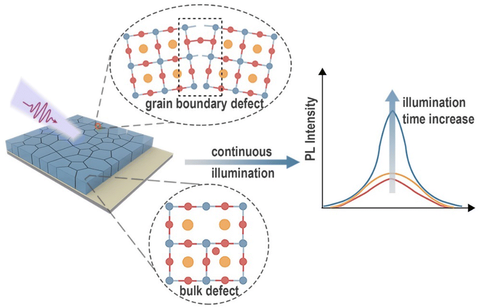 | ||
| Fig. 1 An illustrative diagram of dynamic defect tolerance. With continuous illumination perovskite films exhibit increased PL efficiency and prolonged carrier lifetime. | ||
Time-dependent PL efficiency and carrier lifetime
To study the dynamic response of perovskite thin films under continuous illumination, FA0.85MA0.15Pb(I0.85Br0.15)3 perovskite was prepared using the solution spin-coating method that has been commonly used in the preparation of perovskite solar cells.26–28 Glass and silicone resin were used to encapsulate the sample to isolate moisture and oxygen in the air (as shown in Fig. 2a). The morphology of the sample is shown in Fig. S1 (ESI†), similar to other perovskite films with good coverage and uniform grain size.29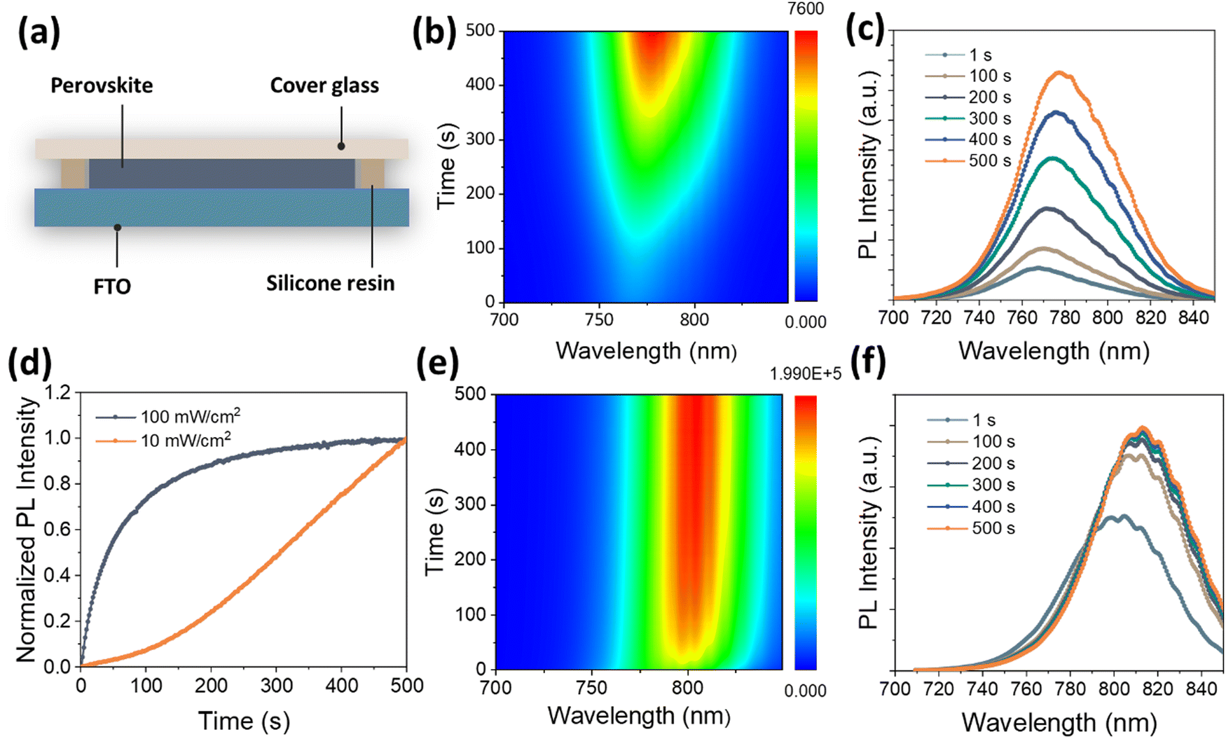 | ||
| Fig. 2 (a) Schematic diagram of the packaging structure of the prepared perovskite films. The continuous illumination time dependent PL spectra under laser excitations at (b) 10 mW cm−2 and (e) 100 mW cm−2. (d) Normalized PL intensity as a function of illumination time. The PL spectra with an illumination time interval of 100 s under laser excitations at (c) 10 mW cm−2 and (f) 100 mW cm−2. | ||
We consecutively measure PL spectra under constant excitation intensity using a fluorimeter with an electrothermal cooled charge-coupled device (CCD) detector, as shown in Fig. 2b. At low excitation of 10 mW cm−2, a distinct peak can be observed around 780 nm (1.59 eV), consistent with the results obtained from UV-vis absorption spectroscopy (Fig. S2, ESI†). In addition, PL enhancement was clearly observed with continuous illumination, as shown in Fig. 2. When increasing the fluence to 100 mW cm−2, the PL enhancement effect is found to be faster and tends to saturate after illumination for 200 seconds (Fig. 2d, e and f), which suggests that this PL enhancement is related to illumination intensity. Furthermore, a pronounced redshift phenomenon can be observed, which can be attributed to I-rich phase formation resulting from I-migration,20 as shown in Fig. 2c and f. The PLQE is essentially determined by the competition between the radiative and non-radiative recombination processes. In our measurement, all the excitation and detection conditions remain identical. Under such specific conditions the detected PL intensity is approximately proportional to the PL efficiency and thus can be used for comparing relative PL efficiency. The unique illumination time dependent PL enhancement indicates the dynamic change in the carrier recombination induced by illumination, leading to a decrease in non-radiative recombination and an enhancement in radiative recombination. Moreover, MAPbI3 and FAPbI3 also showed similar PL enhancement results in illumination time-dependent PL experiments, as shown in Fig. S3 (ESI†). These results indicate that under continuous illumination, a significant defect healing effect and dynamic tolerance to defects is widespread in HOIPs. A similar illumination induced PL enhancement has been previously reported with various interpretations.21,30,31
It is necessary to note that many negative effects caused by illumination have also been commonly observed, such as IV hysteresis,11 phase separation,18 and so on. This does not conflict with our observed PL-enhancement effect since there exists a light exposure threshold between positive and negative effects. With illumination at high intensity, it is expected that the ions from fabrication (such as interstitials) can be activated and escape from the lattice, which can result in negative illumination effects such as PL quenching.21 Under low density illumination, illumination induced local lattice or sublattice distortion or deformation can be dominant, which is likely beneficial to the photoelectric performance of HOIPs because the effects of charge and defect are minimized in this case. The threshold also determines the tolerance of perovskites to defects and depends on factors such as the trap densities and energy level of defects introduced during sample preparation.
The carrier dynamics under continuous illumination
To obtain more detailed insights into the illumination induced PL enhancement, we performed time-dependent TRPL under continuous illumination (405 nm pulsed laser) using a time-correlated single photon counting (TCSPC) technique. The PL decay curves are consecutively extracted as a function of illumination time and then quantitively analyzed. As shown in Fig. 3a and b, the PL decay curves exhibit a double exponential decay. This suggests that at low photon flux, the carrier recombination includes a fast defect-mediated nonradiative recombination and a slow bimolecular recombination. Each PL decay curve can be well fitted using a two-exponential function and the fitting parameters are tabulated in Table S1 (ESI†).32 The fast component
  is mainly due to defect trapping, while the slow component corresponds to bimolecular recombination.21,33 Under low excitation, the defect trapping is very important because the fast component has a significant contribution in the PL decay curve. As shown in Fig. 3c, under continuous excitation at 10 mW cm−2 fluence, the average carrier lifetime increases significantly and tends to be stable at 420 ns after about 200 s, with a decrease in the defect trapping rate corresponding to the fast component. The reduction in the fast decay component means that continuous excitation reduces charge carrier trapping. Increasing the fluence to 100 mW cm−2, the sample exhibited a higher average carrier lifetime and lower charge carrier trapping rate at the initial moment, which can be attributed to the strong electron–phonon coupling and trap state populated rapidly under a high carrier concentration.34,35 Furthermore, under continuous excitation, the defect trapping rate decreases with the increase of illumination time, resulting in the increase of the average carrier lifetime. The trend is the same as that of the 10 mW cm−2 excitation. These dynamic changes in transient optical properties correspond well to previous enhancement of steady-state PL efficiency, further confirming the dynamic defect tolerance characteristics of the prepared perovskite films.
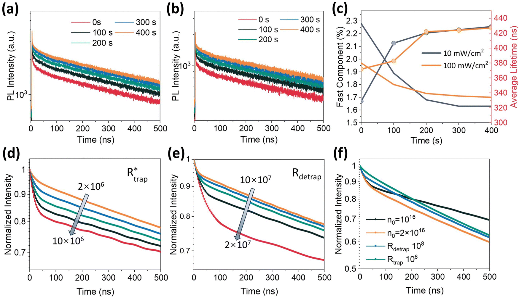 | ||
| Fig. 3 The PL decay traces with different illumination times under excitations at (a) 10 mW cm−2 and (b) 100 mW cm−2, which were detected at 780 nm. (c) The fitted average carrier lifetime and the fast component as a function of time are shown, with scatter lines representing the average carrier lifetime and solid lines representing the fast component. The PL decay curves simulated by rate equation set (1–2): (d) the Rtrap* increases from 2 × 10⁶ to 10 × 106 in the arrow direction, and (e) the Rdetrap increases from 2 × 10⁷ to 10 × 107 in the arrow direction. (f) The PL decay curves simulated under different initial carrier concentrations, Rtrap* and Rdetrap. | ||
The numerical simulation method can help us to further quantitatively analyze the charge carrier trapping dynamics induced by illumination (see the ESI† for detailed simulation processes and parameters). The charge carrier decay dynamic in terms of charge trapping and detrapping can be described using eqn (1–2):18,32,35
 | (1) |
 | (2) |
3. Discussion
The timescales involved in the photoinduced enhancement effect are consistent with the reported lattice and ionic activities, such as migration rates,11 phase segregation,42 and lattice deformation.13,34 These phenomena coexist and compete. The ion-related dynamic behaviors are essentially photochemical reactions between defect sites and carriers which are closely related to the defect trapping/detrapping.43–45 In addition, the defect charge state transitions caused by carrier trapping/detrapping would result in notable reorganization of the local structure of point defects.46,47 Therefore, the observed PL-enhanced features related to carrier concentration and illumination time indicate that long-living structure configuration with slow carrier recombination rates are generated during the complex photochemical reaction competition. To investigate the effect of these photochemical processes on carrier trapping dynamics and the carrier recombination rate, DFT calculations and NAMD simulations were further performed. In the previous section, we have demonstrated that photoinduced dynamic PL enhancement is widely present in various HOIPs, as shown in Fig. 2 and Fig. S3 (ESI†). Therefore, to simplify the computational model, the main component of FA0.85MA0.15Pb(I0.85Br0.15)3, FAPbI3, was selected as the model for subsequent calculation and simulation. What's more, the light-sensitive interstitial and vacancy defects in iodine defects were chosen as the focus of the study.48Before investigating electron–hole (e–h) recombination dynamics, it is instructive to study the ground state properties of various defect systems at 0 K. Fig. 4a and d show that under I-rich conditions, the formation energies of different charge states of vacancy (Iv) and interstitial (Ii) iodine defects as a function of Fermi levels. The +1 charged state of the Iv dominates with the Fermi level for almost the entire bandgap, while the dominant charged state of Ii is +1 (−1) when the Fermi energy level is lower (higher) than 0.68 eV. In the initial equilibrium state (in the dark), the position of the Fermi level depends on the preparation conditions of the sample. According to previous reports, the Fermi level of HOIPs is pinned near VBM under I-rich conditions, which indicates that Iv and Ii mainly exist in the form of +1 charge states.43,44 For non-equilibrium states with continuous illumination, the Fermi level of defective systems would shift due to the charge-state transition of defects caused by the interaction between the trapped charge carrier and the defect site and consequently result in a notable reorganization of the local structure.49 Under the non-equilibrium condition, the Pb–Pb bond length in Iv would change with the charge state transition. When an electron is bound to I+lv and forms I0v, the Pb–Pb bond length decreases from 6.37 to 6.16 Å, and further decreases to 5.94 Å (Form Pb–Pb dimer) by trapping another electron (Fig. 4b). For Ii systems, I+li exhibits a trimer-iodine configuration, which could realize the conversion from trimer iodine to bridge iodine configuration due to local I migration caused by charge state transition from +1 to 0 or −1. The bridge iodine configuration showed a Pb–I bond length of 3.41 and 3.20 Å for 0 and −1 charge states (Fig. 4e). Furthermore, calculation of the density of states (DOS) shows that no obvious DS in Iv systems are observed in the bandgap because the defect level is above CBM,9 which indicates that the charge state transition of Iv has little effect on the carriers recombination rate (Fig. 4c). In the Ii systems, I+li exhibits a deep DS, but it can transform into a shallow p-type DS with electron trapping, which is conducive to the suppression of defect-mediated non-radiative recombination (Fig. 4f). Considering the calculation results of defect formation energy, we speculate that the photoinduced PL enhancement may be attributed to the charge state transition from +1 to −1 assisted by trapped electrons in the Ii system.
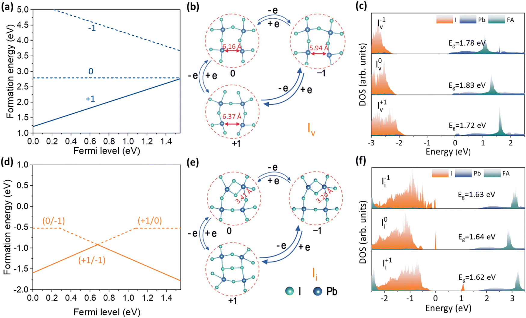 | ||
| Fig. 4 Formation energy of the (−1, 0, +1) charge state defect as a function of Fermi level in Iv (a) and Ii (d) systems. Local configurations of Iv (b) and Ii (e) systems and their transitions via electron trapping and detrapping. The density of state (DOS) for various charge states of Ii (c) and Iv (f) systems. | ||
At finite temperature, the electron–phonon interactions of various charge state structures have an important effect on the electronic structure of the frontier and defect energy levels, which reflect the stability of the corresponding structure. Fig. 5 shows the edge bands and DS energy evolution of each defect system along molecular dynamics (MD) trajectories at 300 K. As shown in Fig. 5a–c, defect Iv at three charge states (+1, 0, −1) resulted in shallow levels near the CBM. The strong energy fluctuation of the defect level in the −1 charge state further indicates that the Pb–Pb configuration is metastable. Therefore, the electron detrapping in I−lv is relatively fast, and the Iv structure is more likely to stabilize in the I+lv, which is in good agreement with the result of defect formation energy. For the Ii, the +1 charge state has a defect level that oscillates vigorously along the MD trajectory, while for (0, −1) the charge states show typical shallow n-type defects and their energy fluctuations are small. The energy oscillation of the I+li defect level can be attributed to the strong fluctuation of the I–I wrong bond length at 300 K temperature.45 In addition, the deeper defect energy levels enable I+li to undergo electron trapping quickly. Under continuous illumination, the metastable trimer iodine would be transformed into I0i of the bridge-iodine configuration by electron trapping. Since the neutral Ii is metastable, I0i could be further transformed into stable I−1i by electron trapping. In addition, shallow p-type I−1I is beneficial for inhibiting defect-mediated non-radiative recombination, which further suggests that photoinduced PL enhancement is more likely to result from the structural transformation of I+lv to I−1i under illumination.
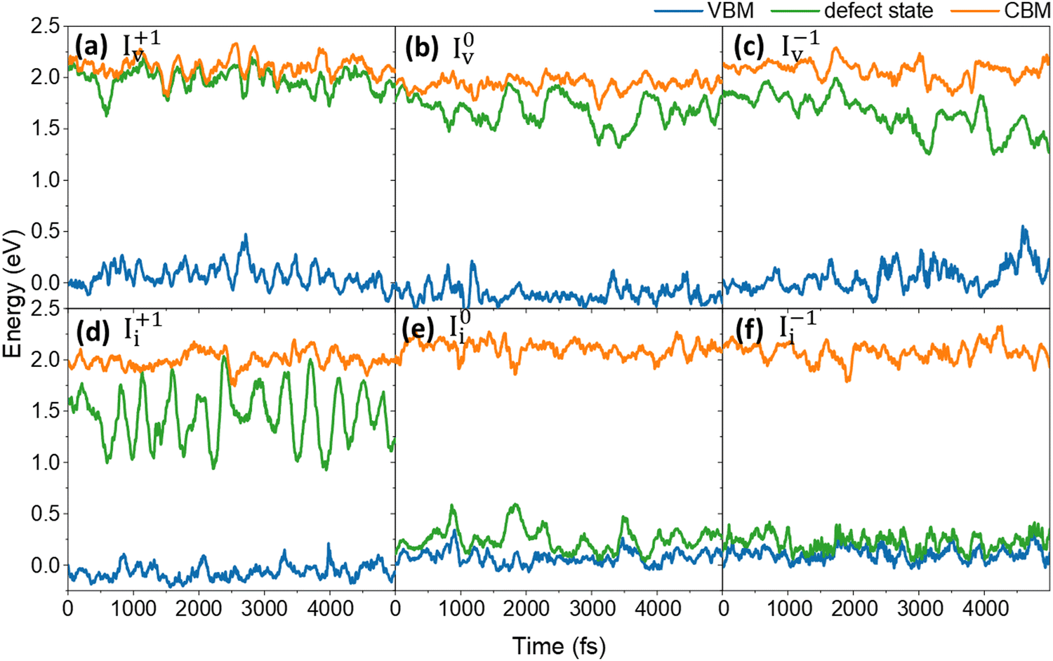 | ||
| Fig. 5 Energy evolution of CBM, VBM and DS along MD trajectories at 300 K. (a)–(c) Iv systems. (d)–(f) Ii systems. The reference energy is set to the initial energy of the VBM. | ||
With the aid of NAMD simulations we can more intuitively understand the change of carrier dynamics caused by charge state transition in each defect system. After photoexcitation, the excited charge carriers can undergo direct recombination with the holes on VBM, or they can undergo a defect-mediated non-radiative recombination, as shown schematically in Fig. 6a. The population evolution of the excited charge carriers on CBM with time is shown in Fig. 6b and c, and the carrier lifetime can be estimated by fitting these curves with the formula f(t) = exp(−t/τ).50 For the Iv system (Fig. 6b), all charge states exhibit a similar e–h recombination rate, and the corresponding carrier lifetimes are 3.86 ns, 3.57 ns and 3.08 ns, respectively. These results indicate that the stable I+lv configuration has a relatively long carrier lifetime, while the photoinduced transition of the charge states from +1 to 0 or −1 instead accelerate carrier recombination. For the Ii system (Fig. 6c), one can clearly see that I−1i has the slowest recombination rate. After 15 ns, the total recombination rates of I+li, I0i and I−1i are 98%, 93.2% and 81.9%, and the corresponding lifetimes are 3.45 ns, 8.03 ns and 11.60 ns, respectively. These results suggest that the carrier recombination rate of Ii decreases when the interstitial iodine structure changes from a trimer in the +1 charge state to a bridge iodine configuration at (0, −1) charge states. Furthermore, the recombination rate of each defect system through different paths was extracted to study the effect of charge state transition on the defect-mediated recombination rate, as shown in Fig. 6d. For all different systems, one can see that non-radiative recombination mediated by defects predominates. What's more, both Iv and Ii systems with non-0 charge states have a relatively fast direct path recombination rate, which can be attributed to the reduced bandgap caused by local lattice distortion of the charged defect (Fig. 4c and f). In Iv systems, the charge state transition from +1 to 0 or −1 does not result in a significant change in the total recombination rate. However, for the Ii system, the transition of charge states from +1 to 0 or −1 significantly reduces the total recombination rate, primarily due to the substantial suppression of defect-mediated non-radiative recombination rates. These results further indicate that the formation of the photoinduced I−1i configuration well meets the necessary conditions for dynamic PL enhancement: (I) long-living structure configuration; (II) slow carrier recombination rate.
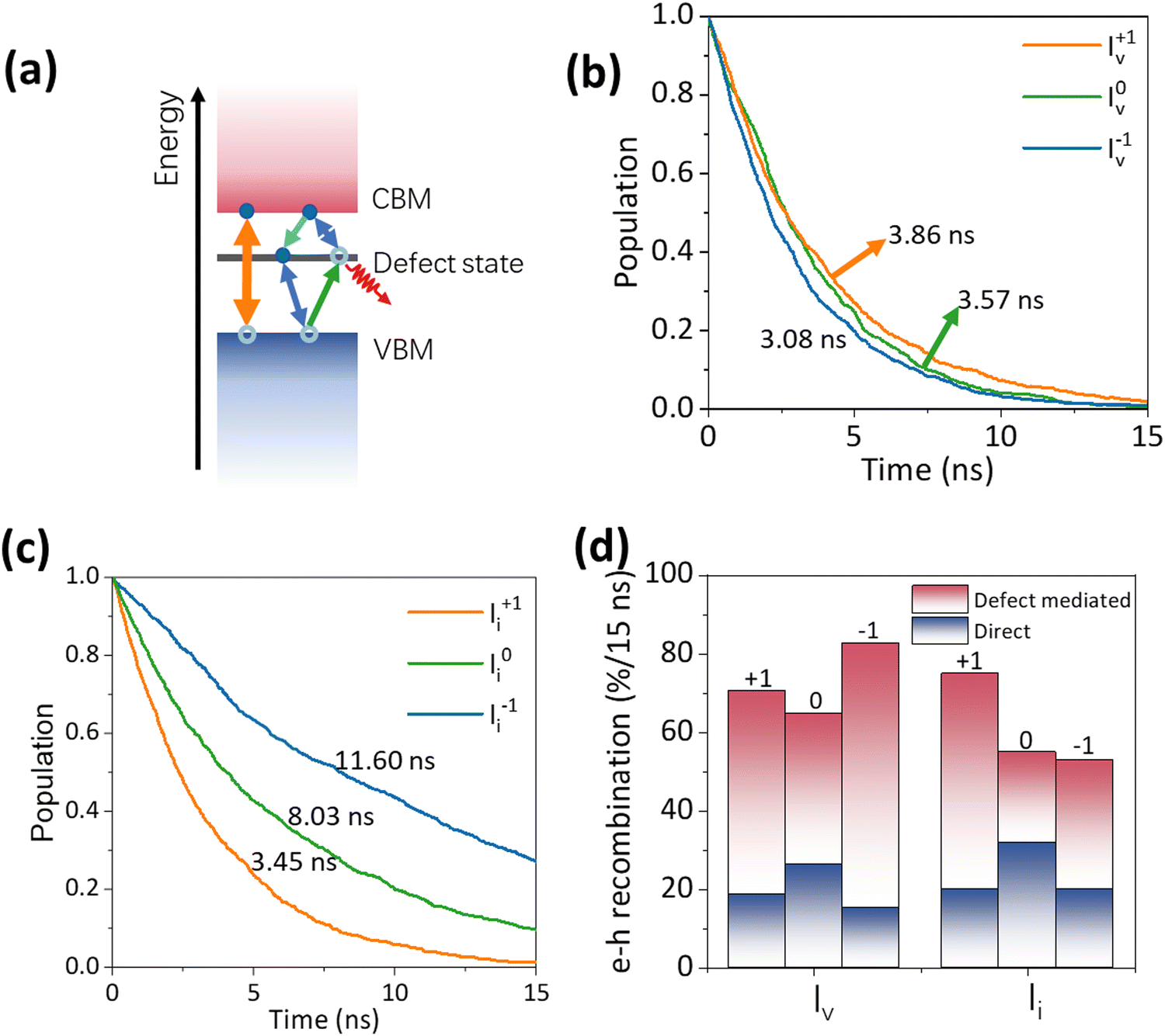 | ||
| Fig. 6 NAMD simulation of different defect systems. (a) Schematic diagram of direct and by defect-assisted path recombination processes. (b) and (c) The population number of excited carriers for Iv and Ii systems at CBM after 15 ns evolution. (d) The percentage of the direct and defect mediated recombination in Iv and Ii systems after 15 ns. | ||
In defective systems, the recombination rate of e–h typically strongly depends on the non-adiabatic coupling (NAC) values between the DS, CBM, and VBM, which determine the probability of electron hopping between different energy levels. Generally, a small NAC value implies slow e–h recombination. The NAC matrix element can be expressed as eqn (3).7,50
 | (3) |
 ; the energy difference of the KS orbitals and the velocity of the nucleus. We extracted the standard average absolute values of the NAC between the KS orbitals of all defect systems along the MD trajectory from VBM−4 to CBM+4 to quantify the coupling strength between the DS, CBM and VBM, as shown in Fig. 7. The specific numerical NAC values are presented in Table S2 (ESI†). As shown in Fig. 7a–c, all charge states in the Iv system exhibit large NAC values between DS and CBM (greater than 0.9 eV), which means that the electrons in the Iv system have relatively fast trapping/detrapping dynamics between DS and CBM, so the variations Pb–Pb bond lengths near the iodine vacancy are relatively fast. This further proves that photoinduced long-living structural configurations cannot exist in Iv systems. For the Ii system, the NAC values of the (+1, 0, −1) charge states between DS and CBM are 1.163 meV, 0.169 meV and 0.147 meV (Fig. 7d–f and Table S2, ESI†). The trimeric configuration of I+li has a larger NAC value between the DS and CBM compared to the bridge configuration of I0i and I−1i, indicating that trimer iodine is prone to structural reorganization through rapid electron trapping under illumination. The relatively large NAC value of I+li can be attributed to the significant variation of the antibonding ppσ* state caused by the vigorous electron–phonon coupling resulted from strong fluctuations in the I–I wrong bonding length.45 In the I−li system, due to the smaller NAC value between DS and CBM, it is difficult for the additional electron bound by Ii to undergo detrapping, which is advantageous for maintaining its long-living structural configuration.
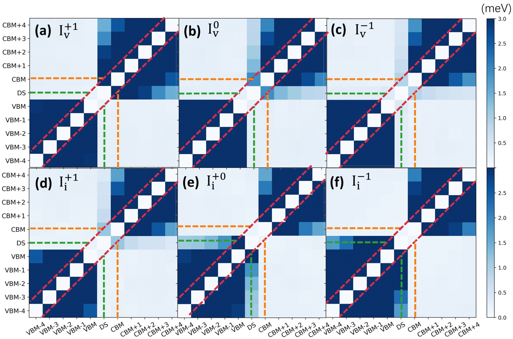 | ||
| Fig. 7 Canonically averaged absolute values of NAC for Iv (a–c) and Ii (d–f) systems from VBM−4 to CBM+4. The color corresponding to the intersection of the red and green dashed lines maps to the NAC value between the DS and VBM. The color corresponding to the intersection of the red and orange dashed lines maps to the NAC value between the DS and the CBM. | ||
Furthermore, the NAC variations caused by electron trapping/detrapping can also be seen from the visual orbital spatial distribution of defects in each charge state, as shown in Fig. S5 (ESI†). For I+lv with a large NAC value (11.464 meV) between DS and CBM, the orbital spatial distribution shows a large wave function overlap between DS and CBM. After I+lv captures electrons, the electrons are localized on DS and decrease the wave function overlap with CBM, thereby reducing NAC. For Ii, in the trimer configuration, the electrons are delocalized and distributed on the three I atoms of the DS. After trapping the electron and transforming it into 0 or −1 charge states, the electrons are localized and distributed on the interstitial iodine atom of the DS and VBM, which significantly decreases (increases) the NAC value between DS and CBM (VBM). The large NAC difference between DS-VBM and DS-CBM would result in a significant difference in the trapping rates of electrons and holes by traps and thus suppressing the non-radiative recombination rate in the DS. In addition, the redistribution of electron density, in turn, also affects the energy fluctuations and shifts of the band edges and DS (Fig. 5a–f).
Electron–phonon interaction plays a key role in the stability of different charge-state structures and carrier dynamics. To provide insights into the electron–phonon interaction, we calculate the Fourier transform of the autocorrelation function of the energy gaps in the defective system (pristine system) between CBM and DS (VBM). The intensity of each peak in the spectrum represents the strength of the electron–phonon coupling at a particular phonon frequency. As shown in Fig. 8a, both pristine and defect systems show dominant frequency modes below 200 cm−1, which is consistent with previous studies.51–53 In the pristine system, the lowest frequency mode (M1: ∼25 cm−1) corresponds to the Pb–I octahedral twist, and the lower frequency phonon modes M2 and M3 should be assigned to the Pb–I–Pb bending and stretching vibration modes, which are in good agreement with previous experimental results (68 cm−1 and 99 cm−1).54,55 For Iv systems, I−lv shows two prominent peaks below 25 cm−1, which can be attributed to large variations of Pb nucleus velocity in Pb dimers. The strong electron–phonon coupling causes excited electrons to convert energy into lattice vibration energy, thereby accelerating carrier relaxation and reducing lattice stability. This further proves that the capture of electrons by the defect state cannot lead to long-lived structures in Iv under illumination. For Ii systems, I+li shows two high-intensity phonon modes at about 80 and 94 cm−1, which should be assigned to the weak wrong I–I bond associated phonon modes. When the charge state transitions from +1 to −1, the electro–phonon coupling is significantly reduced due to the formation of the Pb–I bond and thus the NAC value decreases by about 7 times (Fig. 7). This further supports that under illumination, the charge state transition from +1 in the dark to −1 by electron trapping is conducive to improving the structural stability of Ii and prolonging the carrier lifetime.
 | ||
| Fig. 8 (a) The Fourier transform spectra of the autocorrelation function of the energy difference between the DS and CBM in pristine, Iv and Ii systems. Schematic diagram typical phonon modes: (b) Pb–I octahedral twist, (c) Pb–I–Pb bending, and (d) Pb–I stretching. | ||
Based on these results, the dynamic mechanism of the anomalous photoinduced PL-enhancing effect in HOIPs is shown in Fig. 9. Specifically, (1) under the condition of equilibrium state (in dark), the point defects in different charge states have different stable structure configurations and carrier lifetimes. The initial structure depends on the growth conditions of the sample (chemical potential of the element). (2) In non-equilibrium state, illumination would lead to photochemical reaction and form a new stable defect configuration, resulting in significant changes in carrier lifetime. Under continuous illumination, the gradual increase of components that are beneficial for carrier lifetime in the material induces the illumination time-dependent PL enhancement, such as I+li + e → I0i + e → I−li. (3) The structural transformation related to charge states is driven by electron–phonon interaction, and enhanced electron–phonon interaction would accelerate the reorganization of the local structure, which well explains the PL intensity changes related to photon flux. The local lattice distortion of defects is essentially the short-range migration of ions, and the halogen ion related local ion migration has the most notable influence on the carrier dynamic behavior. The soft lattice and ion lattice properties of HOIPs play an important role in the photoinduced dynamic process, which allows the multiple configurations of perovskite defects in multiple charge states and small ion migration energy barriers.
 | ||
| Fig. 9 Physical mechanism diagram of the photoinduced dynamic defect response in HOIPs under continuous illumination. | ||
Although this interesting light gain phenomenon is a reversible positive effect for perovskite materials, the dynamic change triggered by light is detrimental to the photostability of perovskite-based optoelectronic devices. Therefore, some phenomenology-based and effective strategies have been proposed to suppress this photoinduced dynamic response. (1) Minimizing the defect concentrations. This reduces the photoinduced defect charge state transition and related structural changes.31 (2) Interface engineering. Inhibiting ion migration by anchoring uncoordinated ions at defect sites through Lewis acid or base molecules.56,57 (3) Component engineering. Doping of alkali metal ions at the A site has been widely proven to maximize the migration energy barrier of halogen ions and suppress the local structural distortion induced by light, such as Cs+,58,59 K+,58,60 Rh+. These strategies further confirm that light-induce PL enhancement stems from the fact that local structural reorganization is related to charge state transition. Finally, since the physical understanding of perovskites has significantly lagged in the development of their application technology, more advanced in situ characterization techniques and computational methods are urgently in demand to deeply explore the photoinduced dynamic defect tolerance mechanism in HOIPs, which is of crucial significance for the development of perovskite science and technology.
4. Conclusion
We have demonstrated through time-dependent spectroscopic experiments and simulations that HOIPs have unique photoinduced dynamic defect tolerance, which is manifested in prolonging carrier lifetime and an increasing PL efficiency. The dynamic variation of defect tolerance threshold under illumination is essentially the result of complex photochemical reaction competition induced by illumination, which is closely related to the ion-electron mixed conductor and soft lattice properties of halide perovskite. Under continuous illumination, the defect trapping/detrapping can cause changes in the defect charge state and electron–phonon interaction, driving reorganization of unstable structures to form new stable configurations, resulting in the change of NAC of the defect systems and thus affecting carrier lifetime. The photoinduced dynamic PL enhancement can be attributed to the gradual increase of long-living structures components with longer carrier lifetime under continuous illumination. Our findings provide novel physical understanding for the unusual photoinduced PL enhancement observed for HOIPs from the perspective of the dynamic evolution of defects.Conflicts of interest
The authors declare that they have no conflict of interest.Acknowledgements
The authors acknowledge financial support from the funds for leading local scientific-technological development by the central government (grant no. 202307AB110010) and the Yunling Scholars Fund of Yunnan Province Xing Dian Talents Program (grant no. KC194317). The authors acknowledge financial support from the Australian Research Council FT210100806, DP220100603, CE230100006, and IC180100005. This work was performed in part at The Advanced Analysis and Measurement Center of Yunnan University.References
- Z. Huang, Y. Bai, X. Huang, J. Li, Y. Wu, Y. Chen, K. Li, X. Niu, N. Li, G. Liu, Y. Zhang, H. Zai, Q. Chen, T. Lei, L. Wang and H. Zhou, Nature, 2023, 623, 531–537 CrossRef CAS PubMed.
- H. Li, C. Chen, H. Hu, Y. Li, Z. Shen, F. Li, Y. Liu, R. Liu, J. Chen, C. Dong, S. Mabrouk, R. S. Bobba, A. Baniya, M. Wang and Q. Qiao, InfoMat, 2022, 7, 4 CrossRef PubMed.
- J. F. Liao, W. Q. Wu, Y. Jiang, J. X. Zhong, L. Wang and D. B. Kuang, Chem. Soc. Rev., 2020, 49, 354–381 RSC.
- C. Qiu, L. Wagner, J. Liu, W. Zhang, J. Du, Q. Wang, Y. Hu and H. J. E. Han, EcoMat, 2023, 5, e12268 CrossRef CAS.
- K. X. Steirer, P. Schulz, G. Teeter, V. Stevanovic, M. Yang, K. Zhu and J. J. J. A. E. L. Berry, ACS Energy Lett., 2016, 1, 360–366 CrossRef CAS.
- W. B. Chu, Q. J. Zheng, O. V. Prezhdo, J. Zhao and W. A. Saidi, Sci. Adv., 2020, 6, 8 Search PubMed.
- W. Chu, W. A. Saidi, J. Zhao and O. V. Prezhdo, Angew. Chem., Int. Ed., 2020, 59, 6435–6441 CrossRef CAS PubMed.
- J. Kang and L. W. Wang, J. Phys. Chem. Lett., 2017, 8, 489–493 CrossRef CAS PubMed.
- W.-J. Yin, T. Shi and Y. Yan, J. Phys. Chem. C, 2015, 119, 5253–5264 CrossRef CAS.
- C. Ran, J. Xu, W. Gao, C. Huang and S. J. C. S. R. Dou, Chem. Soc. Rev., 2018, 47, 4581–4610 RSC.
- Y.-C. Zhao, W.-K. Zhou, X. Zhou, K.-H. Liu, D.-P. Yu and Q. Zhao, Light Sci. Appl., 2016, 6, e16243 CrossRef PubMed.
- P. Dong, L. Yang, G. Du, W. Wang, N. Rolston and J. Zhang, Adv. Funct. Mater., 2022, 33, 2211304 CrossRef.
- H. Tsai, R. Asadpour, J. C. Blancon, C. C. Stoumpos, O. Durand, J. W. Strzalka, B. Chen, R. Verduzco, P. M. Ajayan, S. Tretiak, J. Even, M. A. Alam, M. G. Kanatzidis, W. Nie and A. D. Mohite, Science, 2018, 360, 67–70 CrossRef CAS PubMed.
- J. Zhou, Z. Liu, P. Yu, G. Tong, R. Chen, L. K. Ono, R. Chen, H. Wang, F. Ren and S. J. N. C. Liu, Nat. Commun., 2023, 14, 6120 CrossRef CAS PubMed.
- J. J. T. J. o P. C. L. Bisquert, J. Phys. Chem. Lett., 2023, 14, 1014–1021 CrossRef CAS PubMed.
- L. Yin, C. Ding, C. Liu, C. Zhao, W. Zha, I. Z. Mitrovic, E. G. Lim, Y. Han, X. Gao and L. J. A. E. M. Zhang, Adv. Energy Mater., 2023, 13, 2301161 CrossRef CAS.
- Y. Liang, F. Li, X. Cui, T. Lv, C. Stampfl, S. P. Ringer, X. Yang, J. Huang and R. Zheng, Nat. Commun., 2024, 15, 1 Search PubMed.
- H. R. Byun, D. Y. Park, H. M. Oh, G. Namkoong and M. S. Jeong, ACS Photonics, 2017, 4, 2813–2820 CrossRef CAS.
- F. P. Sabino, G. M. Dalpian and A. Zunger, Adv. Energy Mater., 2023, 13, 2301539 CrossRef CAS.
- Y. Zhou, S. C. W. van Laar, D. Meggiolaro, L. Gregori, S. Martani, J. Y. Heng, K. Datta, J. Jiménez-López and F. Wang, Adv. Mater., 2024, 36, 2305567 CrossRef CAS PubMed.
- S. Chen, X. Wen, S. Huang, F. Huang, Y.-B. Cheng, M. Green and A. Ho-Baillie, Sol. RRL, 2017, 1, 1600001 CrossRef.
- J. Xu, A. Maxwell, M. Wei, Z. Wang, B. Chen, T. Zhu and E. H. Sargent, ACS Energy Lett., 2021, 6, 4220–4227 CrossRef CAS.
- W. Nie, J. C. Blancon, A. J. Neukirch, K. Appavoo, H. Tsai, M. Chhowalla, M. A. Alam and M. Y. Sfeir, Nat. Commun., 2016, 7, 11574 CrossRef CAS PubMed.
- F. Z. Huang, L. C. Jiang, A. R. Pascoe, Y. F. Yan, U. Bach, L. Spiccia and Y. B. Cheng, Nano Energy, 2016, 27, 509–514 CrossRef CAS.
- J. S. Park, S. Kim, Z. J. Xie and A. Walsh, Nat. Rev. Mater., 2018, 3, 194–210 CrossRef CAS.
- J. Peng, F. Kremer, D. Walter, Y. Wu, Y. Ji, J. Xiang, W. Liu, T. Duong, H. Shen, T. Lu, F. Brink, D. Zhong, L. Li, O. Lee Cheong Lem, Y. Liu, K. J. Weber, T. P. White and K. R. Catchpole, Nature, 2022, 601, 573–578 CrossRef CAS PubMed.
- J. Chen, H. Dong, J. Li, X. Zhu, J. Xu, F. Pan, R. Xu, J. Xi, B. Jiao, X. Hou, K. Wei Ng, S.-P. Wang and Z. Wu, ACS Energy Lett., 2022, 7, 3685–3694 CrossRef CAS.
- K. Deng, Q. Chen and L. Li, Adv. Funct. Mater., 2020, 30, 2004209 CrossRef CAS.
- T. Bu, J. Li, F. Zheng, W. Chen, X. Wen, Z. Ku, Y. Peng, J. Zhong, Y. B. Cheng and F. Huang, Nat. Commun., 2018, 9, 4609 CrossRef PubMed.
- Z. Andaji-Garmaroudi, M. Anaya, A. J. Pearson and S. D. Stranks, Adv. Energy Mater., 2019, 10, 1903109 CrossRef.
- X. Wu, J. Ma, M. Qin, X. Guo, Y. Li, Z. Qin, J. Xu and X. Lu, Adv. Funct. Mater., 2021, 31, 2101287 CrossRef CAS.
- Z. Gan, X. Wen, C. Zhou, W. Chen, F. Zheng, S. Yang, J. A. Davis, P. C. Tapping, T. W. Kee, H. Zhang and B. Jia, Adv. Opt. Mater., 2019, 7, 1900971 CrossRef CAS.
- Z. Gan, W. Chen, C. Liu, J. Zhang, Y. Di, L. Yu, L. Dong, B. Jia and X. Wen, Adv. Photonics Res., 2021, 3, 2100283 CrossRef.
- H. Zhang, Z. Bi, Z. Zhai, H. Gao, Y. Liu, M. Jin, M. Ye, X. Li, H. Liu, Y. Zhang, X. Li, H. Tan, Y. Xu and L. Yang, Adv. Funct. Mater., 2023, 34, 2302214 CrossRef.
- M. J. Trimpl, A. D. Wright, K. Schutt, L. R. V. Buizza, Z. P. Wang, M. B. Johnston, H. J. Snaith, P. Muller-Buschbaum and L. M. Herz, Adv. Funct. Mater., 2020, 30, 2004312 CrossRef CAS.
- A. K. Al-Mousoi, M. K. Mohammed, A. Kumar, R. Pandey, J. Madan, D. Dastan, M. K. Hossain, P. Sakthivel and Z. M. Yaseen, Phys. Chem. Chem. Phys., 2023, 25, 16459–16468 RSC.
- S. G. Motti, D. Meggiolaro, A. J. Barker, E. Mosconi, C. A. R. Perini, J. M. Ball, M. Gandini, M. Kim, F. De Angelis and A. Petrozza, Nat. Photonics, 2019, 13, 532–539 CrossRef CAS.
- D. W. deQuilettes, W. Zhang, V. M. Burlakov, D. J. Graham, T. Leijtens, A. Osherov, V. Bulović, H. J. Snaith, D. S. Ginger and S. D. Stranks, Nat. Commun., 2016, 7, 11683 CrossRef CAS PubMed.
- H. Choi, J. C.-R. Ke, S. Skalsky, C. A. Castle, K. Li, K. L. Moore, W. R. Flavell and P. Parkinson, J. Mater. Chem. C, 2020, 8, 7509–7518 RSC.
- T.-H.-Y. Vu, W. Chen, X. Deng, C. F. J. Lau, S. Huang, A. Ho-Baillie, B. Jia and X. Wen, J. Phys. Chem. Lett., 2019, 11, 136–143 CrossRef PubMed.
- J. Hu, R. Gottesman, L. Gouda, A. Kama, M. Priel, S. Tirosh, J. Bisquert and A. Zaban, ACS Energy Lett., 2017, 2, 950–956 CrossRef CAS.
- M. C. Brennan, S. Draguta, P. V. Kamat and M. Kuno, ACS Energy Lett., 2017, 3, 204–213 CrossRef.
- X. Zhang and S. H. Wei, Phys. Rev. Lett., 2022, 128, 136401 CrossRef CAS PubMed.
- X. Zhang, J. X. Shen, M. E. Turiansky and C. G. Van de Walle, Nat. Mater., 2021, 20, 971–976 CrossRef CAS PubMed.
- J. Wang, X. Duan and W. J. Yin, J. Phys. Chem. Lett., 2021, 12, 9328–9335 CrossRef CAS PubMed.
- L. Martiradonna, Nat. Mater., 2018, 17, 377 CrossRef CAS PubMed.
- D. Meggiolaro and F. De Angelis, ACS Energy Lett., 2018, 3, 2206–2222 CrossRef CAS.
- M. Ghasemi, B. Guo, K. Darabi, T. Wang, K. Wang, C.-W. Huang, B. M. Lefler, L. Taussig, M. Chauhan, G. Baucom, T. Kim, E. D. Gomez, J. M. Atkin, S. Priya and A. Amassian, Nat. Mater., 2023, 22, 329–337 CrossRef CAS PubMed.
- G. Alkhalifah, A. D. Marshall, F. Rudayni, S. Wanigasekara, J. Z. Wu and W.-L. Chan, J. Phys. Chem. Lett., 2022, 13, 6711–6720 CrossRef CAS PubMed.
- C. J. Tong, L. Li, L. M. Liu and O. V. Prezhdo, J. Am. Chem. Soc., 2020, 142, 3060–3068 CrossRef CAS PubMed.
- Z. Zhou, J. He, T. Frauenheim, O. V. Prezhdo and J. Wang, J. Am. Chem. Soc., 2022, 144, 18126–18134 CrossRef CAS PubMed.
- C.-J. Tong, L. Li, L.-M. Liu and O. V. Prezhdo, ACS Energy Lett., 2018, 3, 1868–1874 CrossRef CAS.
- C. J. Tong, X. Cai, A. Y. Zhu, L. M. Liu and O. V. Prezhdo, J. Am. Chem. Soc., 2022, 144, 6604–6612 CrossRef CAS PubMed.
- C. Quarti, G. Grancini, E. Mosconi, P. Bruno, J. M. Ball, M. M. Lee, H. J. Snaith, A. Petrozza and F. De Angelis, J. Phys. Chem. Lett., 2013, 5, 279–284 CrossRef PubMed.
- M. A. Pérez-Osorio, R. L. Milot, M. R. Filip, J. B. Patel, L. M. Herz, M. B. Johnston and F. Giustino, J. Phys. Chem. C, 2015, 119, 25703–25718 CrossRef.
- L. Yang, M. Wu, F. Cai, P. Wang, R. S. Gurney, D. Liu, J. Xia and T. Wang, J. Mater. Chem. A, 2018, 6, 10379–10387 RSC.
- C. Yang, Z. Hu, C. Gao, Y. Wang, H. Zhang, J. Wang, J. Zhang, X. Zhou and Y. Zhu, J. Phys. Chem. C, 2019, 124, 1851–1860 CrossRef.
- H. Wu, C. Xu, Z. Zhang, Z. Xiong, M. Shi, S. Ma, W. Fan, Z. Zhang, Q. Liao, Z. Kang and Y. Zhang, Nano Lett., 2022, 22, 1467–1474 CrossRef CAS PubMed.
- B. Li, M. Lin, C. Kan, P. Hang, Y. Yao, Z. Hu, Y. Wang, Y. Zhang, W. Zhong, D. Yang and X. Yu, Sol. RRL, 2022, 6, 2200050 CrossRef CAS.
- F. Zheng, W. Chen, T. Bu, K. P. Ghiggino, F. Huang, Y. Cheng, P. Tapping, T. W. Kee, B. Jia and X. Wen, Adv. Energy Mater., 2019, 9, 1901016 CrossRef.
Footnote |
| † Electronic supplementary information (ESI) available. See DOI: https://doi.org/10.1039/d4tc01578a |
| This journal is © The Royal Society of Chemistry 2024 |