
 Open Access Article
 This Open Access Article is licensed under a
 Creative Commons Attribution 3.0 Unported Licence
Computational prediction and characterization of CuI-based ternary p-type transparent conductors†
Michael
Seifert
 a,
Tomáš
Rauch
a,
Miguel A. L.
Marques
bc and
Silvana
Botti
*ad
a,
Tomáš
Rauch
a,
Miguel A. L.
Marques
bc and
Silvana
Botti
*ad
aInstitut für Festkörpertheorie und -optik, Friedrich-Schiller-Universität Jena and European Theoretical Spectroscopy Facility, Max-Wien-Platz 1, 07743 Jena, Germany
bResearch Center Future Energy Materials and Systems of the Research Alliance Ruhr, Faculty of Mechanical Faculty of Mechanical Engineering and ICAMS, Ruhr University Bochum, Universitätstrasse 150, 44780 Bochum, Germany
cEuropean Theoretical Spectroscopy Facility, Germany
dResearch Center Future Energy Materials and Systems of the Research Alliance Ruhr, Faculty of Physics and ICAMS, Ruhr University Bochum, Universitätstrasse 150, 44780 Bochum, Germany. E-mail: silvana.botti@rub.de
First published on 23rd April 2024
Abstract
Zinc blende copper iodide is a natural p-type semiconductor that shows promise for transparent electronics, as it combines outstanding transmission of visible light with high hole mobilities. Despite that, remaining challenges still hinder its use in practical applications. To tackle this problem, chalcogen doping has been proposed and tested as a viable approach to enhance hole concentration. To further tune the electronic properties of this transparent semiconductor, we explore here the ternary phase diagram of copper and iodine with sulfur or selenium across the whole composition range. Performing structure prediction calculations using the minima hopping method, we predict 11 stable crystalline ternary structures, 9 of which are unreported. Based on our band structure calculations, we identify among these compounds 4 interesting candidates for p-type transparent materials and we propose alloying of iodine with a chalcogen atom as a way to control the hole concentration. Additionally, we reveal unreported metallic phases with intriguing topological properties. Our findings broaden the scope of potential applications of CuI-based materials, highlighting the possibility of harnessing their unique electronic characteristics in diverse electronic devices and systems.
1 Introduction
Crystalline materials that combine a high electrical conductivity with complete transparency in the visible portion of the electromagnetic spectrum will be crucial components of future transparent electronics and enable innovative technologies, such as transparent electrodes,1 transparent thin-film transistors,2 solar windows,3 or electrochromic displays.4 The development of transparent displays and transparent electronics, in general, is expected to generate a billion dollar market within the next decade.5,6 For such applications, both electron and hole transparent conducting materials (TCMs) are needed. However, whereas high-performing n-type TCMs, like ZnO7 or indium-tin oxide8,9 are already well established, p-type counterparts are still lacking.5,6,10,11In this context, CuI has been attracting increasing attention as a multifunctional p-type semiconductor.12 In fact, the zinc blende γ-phase of CuI displays high hole mobilities (μ > 40 cm2 V−1 s−1)3 and a band gap of around 3.1 eV.12 In bulk crystals, hole densities of around 1 × 1016 cm−3,13 were observed, while for thin films higher hole concentrations of 1 × 1019 cm−3 to 1 × 1020 cm−3,5,14,15 were reported. The combination of a large band gap and intrinsic holes with high mobilities makes this system a p-type degenerate semiconductor16 and therefore a good candidate p-type TCM.12,16,17 It was furthermore demonstrated that γ-CuI provides ideal compatibility with numerous n-type transparent materials.14,18–20 For example, transparent diodes made of p-CuI and n-ZnO14 were reported to have rectification ratios as large as 109 (±2 V). Compared with diodes made of disordered phases, the latter values imply an improvement by two orders of magnitude. Thin-film transistors and displays were successfully established using p-type CuI thin films.2,5,21,22 Possible applications for ultraviolet photodetectors as well as piezoelectric nanogenerators were also discussed.5,23,24 Measured excitonic binding energies of around 60 meV25 indicate in addition potential for optoelectronic devices: it was already proposed to use CuI in blue and UV LEDs.5,26,27 CuI thin films were as well successfully inserted as hole-collecting layers in perovskite solar cells5,28 and promising results regarding photovoltaic efficiency and stability are described in ref. 29 and 30 CuI films are also by far the best-known transparent p-type thermoelectric with a figure of merit of ZT = 0.21 at 300 K,3 thanks to the heavy anion and strong phonon scattering.5 Furthermore, in contrast to most used thermoelectric materials, CuI is nontoxic, and therefore suitable for thermoelectric windows, body-heat-driven wearable electronics, as well as on-chip cooling.3,5
Despite the already good properties of CuI, there is still a need for further improvement before this p-type TCM can compete with its n-type TCM counterparts. Its main deficiency remains the hole conductivity that is still at least 100 times smaller than the one of n-type TCMs. To enhance the conductivity σ, according to the formula σ = enhμh (where e is the electron charge) it is necessary to increase either the hole (h) charge carrier concentration nh or the mobility μh. The hole mobility, in turn, is proportional to the carrier scattering time and inversely proportional to the hole effective mass. The crystalline quality of the sample plays an important role in increasing the scattering time, while the valence band dispersion yields the transport effective mass. Experimental evidence points to the fact that the film quality can be only marginally improved.5 According to ref. 31 concerning TiO2 incorporation in CuI, an increased hole density leads to reduced resistivity, beneficial for the application of CuI in electronics.
It is therefore worth considering with priority the route of controlling the hole concentration by doping, as well as further reducing the hole effective mass by building CuI-based ternary compounds and alloys. Computational screening of suitable dopant and alloy elements is an effective approach for identifying chemical elements for ternary CuI-based materials with the desired optoelectrical properties.32–34 Predictive ab initio calculations can help experimentalists to prioritize the synthesis and characterization of the most promising materials, uncovering shortcuts to integrate optimized materials into new transparent devices.
It is well known that CuI admits a large range of concentrations of Cu vacancies and that this defect is responsible for p-type conductivity in intrinsic samples.32,35–37 Recently, sulfur and selenium substitutions on the iodine site were identified as the only relatively shallow acceptors for further p-type doping of CuI.32,38 Both S and Se substitutions were predicted to have low formation energies and lead to higher hole concentrations than Cu vacancies.32 Moreover, moderate S and Se doping does not modify significantly neither the absorption spectrum of CuI nor the hole effective masses and therefore the improved hole concentration can potentially positively impact conductivity without deteriorating transparency.39 Following the computational predictions, doping of CuI with Se40 and S41 was experimentally demonstrated and, in the case of S doping, already successfully applied in the context of device fabrication.
It remains an open question if higher concentrations of chalcogen substitutions, beyond the doping limit, i.e. leading to the formation of a ternary ordered or disordered alloy, can have beneficial effects on conductivity and transparency. In experiments, Se doping of CuI at concentrations larger than 1 at% leads to significant changes of the electronic properties,40 hinting at a phase transition to a ternary material. Ternary phases containing Cu and I together with S or Se are however not included in materials databases.42 To shed light on the possibility of forming ordered ternary compounds and disordered alloys, we investigate here the ab initio phase diagrams of Cu–S–I and Cu–Se–I, using the minima hopping method (MHM)43,44 with energies and forces determined by density functional theory (DFT). The MHM allows us to search in an unbiased way for new crystal structures, expanding significantly the search space in comparison to previous works on CuI alloys focused on zinc blende phases.45–47 Following this path, we expect to find new compounds with promising properties and unveil alternative ways to control the electronic properties of CuI-based TCM.
Our article is structured as follows. First, we discuss the convex hulls of thermodynamic stability at T = 0 for CuI-based ternaries, uncovering unreported ternary phases. From the inspection of the obtained phase diagrams, we derive a list of candidate stable or quasi-stable ternary systems. These structures are subsequently subjected to further characterization to evaluate their electronic, transport and optical properties using state-of-the-art density functional theory with hybrid functionals. We classify in this way the different structures according to their structural and electronic properties, revealing semiconductors, metals, and topological semimetals. Collecting all this information, we can finally judge the potential of the new compounds for applications as p-type transparent conductors. Our analysis discloses the relationship between structural and electronic properties in CuI-based materials, offering precious insight to guide future experimental work.
2 Computational details
To calculate the ternary phase diagrams and uncover stable crystalline phases, one has to explore the chemical and configuration space to find the low-lying minima of the adiabatic potential energy surface, considering all possible stoichiometries and crystal structures in which atoms can be arranged. At zero temperature, the convex hull of thermodynamic stability is the convex set of low-energy phases that can not decompose thermodynamically into other compounds. To efficiently detect the lowest-energy structures we used the minima hopping method (MHM).43,44 This is a global structure-prediction algorithm designed to determine the most favourable crystal structures of a system given its chemical composition. At a fixed pressure, the enthalpy hypersurface is sampled by performing consecutive short molecular dynamics escape steps followed by local geometry relaxations, taking into account both atomic and cell variables. The initial velocities for the molecular dynamics trajectories are chosen approximately along soft-mode directions, allowing effective escapes from local minima toward low-energy structures. Revisiting already-known crystal structures is avoided by a feedback mechanism. The MHM has already been used for structural prediction in a wide range of materials, including Cu–I binaries,37 with remarkable results.34,49–52The MHM relies on an underlying theory to calculate energies and forces. We used for this purpose the framework of DFT, with projector augmented wave method (PAW) setups53 as implemented in the software VASP (Vienna ab initio simulation package).54,55 The Cu 3p, 4s and 3d electrons, I 5s and 5p electrons, as well as the s and p electrons of the outermost shell of the chalcogen atoms were treated explicitly in the valence. For the structural prediction runs, we used default cutoff values for the plane-wave basis and we chose a k-point density of 0.025 in reciprocal units. All forces were converged to better than 5 meV Å−1. To approximate the exchange–correlation functional (XC) of density functional theory we used the Perdew–Burke–Ernzerhof56 (PBE) generalized gradient approximation.
To avoid biases induced by the starting configurations, the MHM runs were started from single random configurations. To exclude unphysical starting configurations, the distance between pairs of atoms was always constrained to be larger than the sum of the covalent radii of the corresponding atoms. We performed structural prediction runs for a large selection of stoichiometries, considering unit cells with up to a maximum of 8 atoms. The complete list of considered compositions is given in Table S1 of the (ESI†). The MHM runs were stopped when 70 minima per stoichiometry were found. We remark that in these simulations there is no guarantee that the global minimum is reached, as we cannot exclude that a lower-lying minimum is not sampled or that larger unit cells with the same stoichiometry would lead to lower formation energies per atom, e.g., by decreasing their internal energy through geometry distortions. We are moreover neglecting the contribution of entropy that can stabilize disordered alloys rather than ordered crystals at finite temperatures. However, despite these limitations, several predictions obtained with this method have been confirmed by experiments (see, e.g., the synthesis of the ferroelectric perovskite LaWN357 five years after its prediction58).
To refine the low-energy crystal structures found during the MHM runs, an additional DFT relaxation step was performed with stricter convergence criteria. To this end, we used a denser k-point grid to satisfy a convergence threshold of 1 meV per atom and all structures were relaxed until forces were smaller than 1 meV Å−1. A plane-wave basis set with a cutoff energy of 700 eV was used for all structures, both for this refinement step and for all subsequent electronic-structure calculations.
To build the convex hull, we considered the binary and ternary phases included in the Materials Project database,42 complementing these structures with others that we have identified in previous studies and that are contained in our database.48,59 We recalculated the energy of all structures with our own set of parameters and convergence criteria for consistency. For these structures found on the convex hull, or up to 30 meV per atom above it, we repeated the DFT geometry optimization and the calculation of the formation energy using the PBEsol60 and SCAN61 functionals, with 8000 k-points per reciprocal atom. PBEsol is a version of PBE optimized for solids and SCAN is a meta-GGA functional designed to follow 17 exact constraints of the exchange–correlation functional. We considered these functionals in addition to PBE, as it is well known that formation energies can bear significant errors with this widely-used approximation.48,62–65 The expensive MHM runs were not repeated, but the geometry optimisation and the evaluation of the formation energy of low-energy phases obtained by the MHM search.
To extract the effective masses of the different phases, we considered the symmetry points obtained using SeeK-path66 and we calculated the band structure along these symmetry lines using the PBE approximation. For all semiconducting phases, we further calculated band structures with the hybrid functional HSE06, using an adjusted value of α = 0.32 to reproduce the experimental band gap of CuI of 3.1 eV.67 We refer to the HSE06 with this tuned value of α as “modified HSE06”. As the band gap is sensitive to the localization of Cu d-states that hybridize with anion p-states at the top of the valence band,68 and the modified HSE06 functional properly accounts for the localization of the Cu d-states, we expect that using this modified HSE06 functional can yield accurate band structures also for CuI-based ternaries. For the evaluation of the band gaps, we remind that PBE band gaps are usually underestimated by at least 50%, while hybrid functionals yield reliable predictions.69,70 We applied the modified HSE06 instead of PBE0, as some of the band structures discussed in the manuscript have the chemical potential inside the valence band. It is known that PBE0 gives a vanishing density of states in such cases, due to the unscreened Hartree–Fock exchange energy incorporated in the functional, while the HSE06 or modified versions of it are known to be more robust in such cases.70 The effective masses were fitted using even polynomials of 6th order, E(k) = ak6 + bk4 + ck2 + d, considering an energy range of 25 meV (corresponding to the value of kBT for T = 300 K) around the Γ-point. We also calculated the dielectric functions in the independent-particle approximation, i.e. employing the Fermi golden rule and neglecting local field effects. A Lorentzian broadening of 0.1 eV was applied to the spectra. For Cu3SI2 a 11 × 10 × 16 k-point grid was used for the calculation of the dielectric function.
We used the AMSET code71 to calculate the scattering rates from various mechanisms in the momentum relaxation time approximation (MRTA) to the Boltzmann equation. The scattering rates are then further processed to obtain transport properties such as mobility or conductivity. In our case, many systems turn out to be p-type degenerate semiconductors and the presence of intrinsic free carriers in the ternary materials of interest prevents calculations within the MRTA. In view of that, for those cases, we adopted the constant relaxation time approximation (CRTA). It has been shown in ref. 38 that in γ-CuI a constant τ = 10 fs yields a room-temperature mobility μ comparable to the one obtained from MRTA calculations that treat scattering mechanisms explicitly. We therefore assume this value of τ in our transport calculations within CRTA for the ternary CuI-based compounds. It can be argued that in ternary disordered alloys, smaller scattering times can be expected due to the additional contribution of alloy disorder to the total scattering time, following the Matthiessen rule. For a better comparison, we therefore provide relative mobilities μh/τ and conductivities σ/τ, using the fact that τ is a multiplicative constant in the CRTA. The first-principles input for all transport calculations was obtained with the PBEsol functional including spin–orbit coupling (as done in ref. 38). For γ-CuI the scissor operator, extracted from modified HSE06 calculations, was applied in AMSET to correct the underestimated PBEsol band gap. We note that our MRTA-PBEsol calculations for γ-CuI (μh = 44.56 cm2 V−1 s−1 and μh = 22.85 cm2 V−1 s−1 for nh = 1016 cm−3 and nh = 1020 cm−3, respectively), as well as CRTA-PBEsol calculations (μh = 25.46 cm2 V−1 s−1 and μh = 26.68 cm2 V−1 s−1 for nh = 1016 cm−3 and nh = 1020 cm−3, respectively) are consistent with MRTA-PBE0/PBEsol results in ref. 38 (μh = 41.3 cm2 V−1 s−1 and μh = 32.6 cm2 V−1 s−1 for nh = 1016 cm−3 and nh = 1020 cm−3, respectively) at room temperature.
3 Results
3.1 Ternary phase diagrams
The ternary phase diagrams calculated with PBE, PBEsol and SCAN are shown in Fig. 1 for both Cu–S–I and Cu–Se–I. In addition to the obtained structures from the MHM run, we included CuSe3I from the Materials Project database,42,74 CuSe2I from ref. 48 and CuS2I, obtained from CuSe2I by replacing Se with S. Those phases could not be obtained in the MHM runs since their unit cells are larger than the ones we considered in our calculations. A full list of the considered stoichiometries is given in Table S1 of the ESI.† For each stoichiometry, we found several potential structures. In Fig. 1 we show the distance to the convex hull of the systems with the lowest energy (i.e. the energetically most favourable phases) at the considered compositions. Regarding binary phases, we show in the phase diagrams just the strictly stable ones extracted from ref. 48 and 42.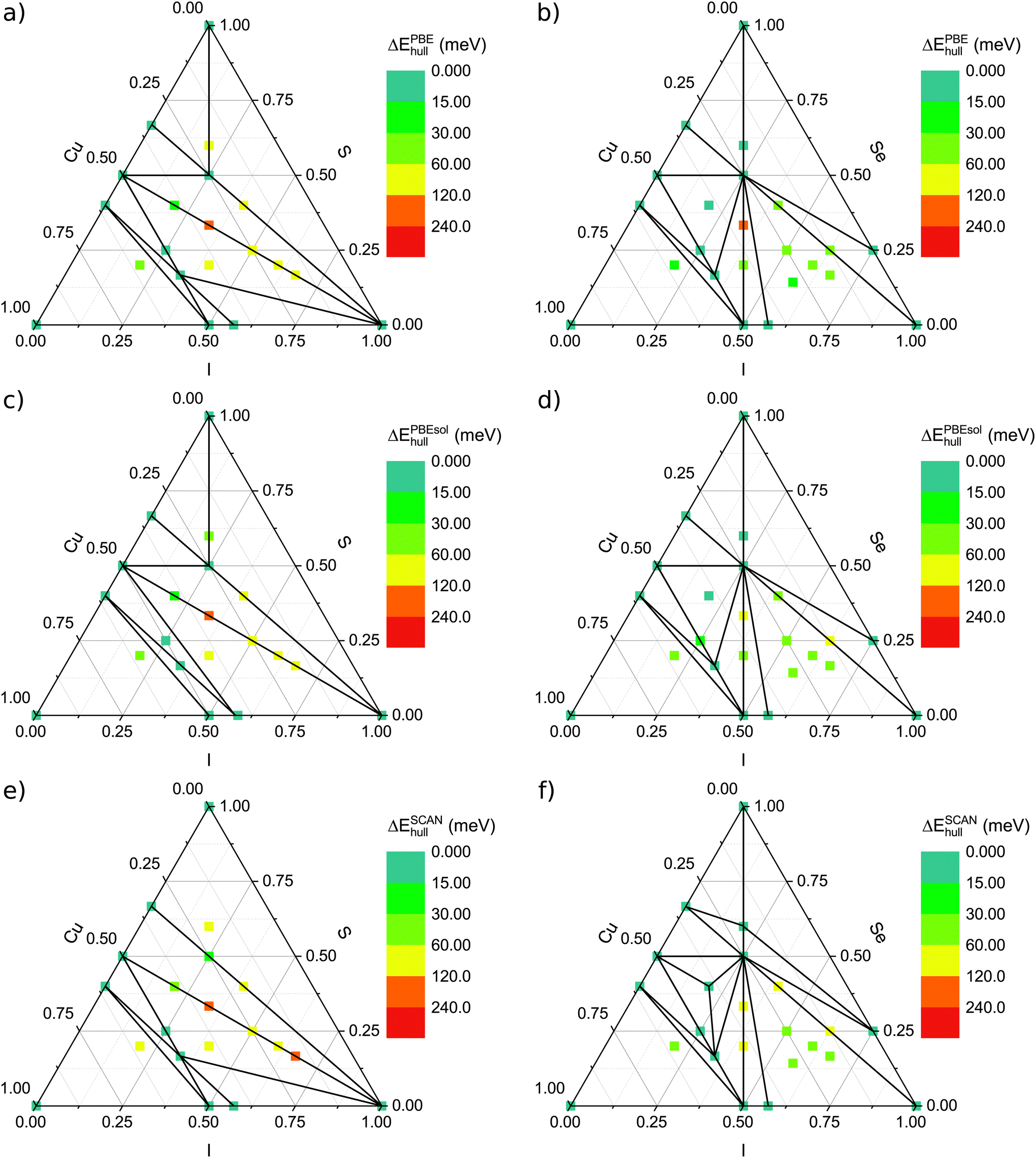 | ||
| Fig. 1 Ternary phase diagrams for Cu–S–I (panels a, c and e) and Cu–Se–I (panels b, d and f) calculated with DFT and the MHM, as explained in the text. The points denote the compositions that we studied and the colour scheme conveys the energy difference to the convex hull of stability. To evaluate the formation energies on the convex hull different XC-functionals were applied: PBE (a) and (b), PBEsol (c) and (d) and SCAN (e) and (f). Finally, the solid lines connect vertices of the convex hull, i.e., compositions that are thermodynamically stable. As reservoir compounds, we used all materials from ref. 48 and 42. | ||
In the case of sulfur, we find a region with several stable phases on the line connecting the binaries CuI and CuS. In the case of selenium, this applies as well, but there are additional structures close to the hull. Furthermore, one can see that in the iodine-rich region of the phase diagrams the compounds containing S have a larger distance to the hull than those containing Se. This is already true for the binary phases, and in particular, there are no stable phases along the S–I line.
Comparing the results obtained with the three functionals (PBE, PBEsol and SCAN), we observe only small numerical differences and no qualitative deviations for the convex hulls. Nevertheless, numerical differences can be large enough to change the situation of a compound from being on the hull to being just close to the hull or vice versa. The energy changes due to the use of another functional varies from case to case, but performing an arithmetic average for the hull energies of all compounds, the SCAN values are overall the largest and the PBE values the smallest.
The exact values of the formation energies, the energy differences to the convex hull and the most likely dissociation channels are reported in Table 1 for the ternaries that lie within 30 meV per atom (according to PBE calculations) from the convex hull. Concerning the ternary phase diagram including sulfur, we identify two structures, namely Cu3SI2 and CuS2I, that are located on the convex hull. In the case of the Cu–Se–I phase diagram, beside Cu3SeI2 (but in a distinct structure) and CuSe2I, we find two further stable phases: CuSe3I and Cu2Se2I. The only phase which is exactly on the hull for all functionals is CuSe2I, but as it can be seen in Table 1, the other phases are either on the hull or very close to it. In total 11 structures appear at a distance of less than 25 meV per atom from the convex hull using the PBE functional. Among them, only 2 were previously reported: CuSe3I74 and CuSe2I.48 An overview of the formation energies and distances from the convex hull for all the considered stoichiometries can be also found in Section II the ESI.†
| Composition | SG | E for | ΔEPBEhull | ΔEPBEsolhull | ΔESCANhull | Dissociating in |
|---|---|---|---|---|---|---|
| Cu3SI2 | 44 | −179 | 0 | 3 | 4 | Cu2SI + CuI |
| CuS2I | 14 | −118 | 0 | 0 | 23 | — |
| Cu2SI | 115 | −180 | 4 | 9 | 11 | Cu3SI2 + CuS |
| Cu2S2I | 187 | −143 | 18 | 16 | 37 | Cu3SI2 + SCu + CuS2I |
| CuSe2I | 14 | −133 | 0 | 0 | 0 | — |
| Cu3SeI2 | 8 | −152 | 0 | 4 | 1 | — |
| Cu2SeI | 115 | −137 | 9 | 17 | 11 | Cu3SeI2 + SeCu |
| CuSe3I | 166 | −94 | 12 | 6 | 0 | — |
| Cu2Se2I | 166 | −124 | 12 | 11 | 0 | — |
| Cu2SeI4 | 8 | −85 | 24 | 36 | 38 | CuSe2I + CuI + SeI3 + I |
| Cu3SeI | 8 | −100 | 25 | 41 | 35 | CuI + Cu3Se2 + Cu |
For the crystal structures directly on the hull, we calculated reaction energies of the ternary compounds with O2 and H2, as well as with Cu, I and Se using the SCAN functional (see Table 2). All the structures interact strongly with both oxygen and hydrogen. It appears therefore extremely important to guarantee an oxygen-free and hydrogen-free environment during the fabrication process. The excess of iodine does not seem to be critical as CuSe2I does not decompose at all and the other two compounds have a small negative reaction energy. On the other hand, in the case of Cu2Se2I the reaction energy in excess of Se is relatively high. This implies that controlling the right amount of Se for obtaining this specific phase could be a challenge. We remark that these calculations neglect reaction dynamics and are performed at 0 K, neglecting entropic terms.
| Composition | Reaction equation | Reaction energy | |
|---|---|---|---|
| Total (eV) | Per f. u. (eV) | ||
| CuSe2I | 15O2 + 4CuSe3I → 2Cu(IO3)2 + 2CuSe2O5 + 4SeO2 | −29.114 | −7.279 |
| 3H2 + CuSe2I → HI + 2H2Se + CuH | −4.076 | −4.076 | |
| CuSe2I + Cu → Cu2Se2I | −0.215 | −0.215 | |
| CuSe2I + Se → CuSe3I | −0.023 | −0.023 | |
| Does not decompose with an excess of I | — | — | |
| CuSe3I | 19O2 + 4CuSe3I → 2Cu(IO3)2 + 2CuSe2O5 + 8SeO2 | −38.296 | −9.574 |
| CuSe3I + H2 → H2Se + CuSe2I | −1.611 | −1.611 | |
| 2CuSe3I + Cu → CuSe2 + 2CuSe2I | −0.289 | −0.145 | |
| Does not decompose with an excess of Se | — | — | |
| CuSe3I + 3I → SeI3 + CuSe2I | −0.030 | −0.030 | |
| Cu2Se2I | 19O2 + 4Cu2Se2I → 2Cu(IO3)2 + 2CuSe2O5 + 4CuSeO4 | −36.438 | −9.110 |
| 7H2 + 2Cu2Se2I → 2HI + 4H2Se + 4CuH | −8.874 | −4.437 | |
| Cu2Se2I + 2Cu → Cu3Se2 + CuI | −0.366 | −0.366 | |
| Cu2Se2I + 3Se → CuSe2 + CuSe3I | −0.143 | −0.143 | |
| Cu2Se2I + I → CuI + CuSe2I | −0.048 | −0.048 | |
3.2 Structural and electronic properties
We now characterize in more detail the structural and electronic properties of the predicted ternary compounds. First, we discuss general trends of the properties of the whole set of CuI-based materials. Afterwards, in Section 4, we subdivide the materials into families with similar structural and electronic properties, to extract from our calculations design rules for Cu(S,Se)I ternary alloys.A summary of the structural parameters is given in Table 3. Pictures of the crystal structures are given in Fig. S2 and in the ESI.† With the exception of Cu3SeI2, all bond lengths between Cu and I atoms are very similar. This holds also for the bonds between Cu and S or Cu and Se. The distances between Cu and I are consistently larger than those between Cu and the chalcogen. This can be explained by the larger ionic and covalent radius of I, compared to the corresponding values for Se and S.75 Only two structures (CuSe3I and Cu2SeI4) contain bonds connecting a chalcogen and iodine, as the anions are usually separated by copper atoms. Another possibility when the number of anions in the formula unit is significantly larger than the number of Cu atoms is the formation of bonds between chalcogen atoms. Interestingly, both Cu3SeI2 and Cu3 SeI crystallize in layered structures, with Cu atoms sandwiched between the anions. These structures are not related to the layered β-phase of CuI observed by Sakuma.67,76 CuS2I and CuSe2I have also layered structures and present S–S and Se–Se bonds.
| Composition | SG | Cu–I (Å) | Cu–X (Å) | I–X (Å) | X–X (Å) | Dimensions |
|---|---|---|---|---|---|---|
| Cu3SI2 | 44 | 2.65 | 2.21 | — | — | 3 |
| 2.74 | 2.25 | — | — | |||
| CuS2I | 14 | 2.61 | 2.27 | — | 1.97 | Layered |
| Cu2SI | 115 | 2.67 | 2.25 | — | — | 3 |
| Cu2S2I | 187 | 2.62 | 2.29 | — | 2.15 | 3 |
| CuSe2I | 14 | 2.61 | 2.40 | — | 2.31 | Layered |
| — | — | — | 2.58 | |||
| Cu3SeI2 | 8 | 2.60 | 2.43 | — | — | Layered |
| 2.82 | 2.40 | — | — | |||
| 3.01 | — | — | — | |||
| Cu2SeI | 115 | 2.66 | 2.37 | — | — | 3 |
| CuSe3I | 166 | 2.68 | 2.42 | 3.61 | 2.40 | 3 |
| Cu2Se2I | 166 | 2.59 | 2.41 | — | 2.43 | 3 |
| Cu2SeI4 | 8 | 2.60 | 2.45 | 2.64 | — | Layered |
| 2.72 | 2.57 | — | — | |||
| Cu3SeI | 8 | 2.60 | 2.61 | — | — | Layered |
| 2.81 | 2.53 | — | — | |||
| — | 2.41 | — | — | |||
| CuI | 216 | 2.63 | — | — | — | 3 |
After this brief overview of structural properties, we move to the characterization of electronic properties. To check if the novel ternary compounds may be suitable for applications as p-type TCMs we calculated their band structures. A list of band gaps Eg, obtained using the PBE and the modified HSE06 functional is shown in Table 4. Note that we used the hybrid functional HSE06 with a modified parameter α = 0.32 if the compound is a semiconductor or a p-type degenerate semiconductor, i.e. with a band structure similar to the one of CuI but with the Fermi energy below the valence band maximum (VBM, see also Section I of the ESI† for the definition of a p-type degenerate semiconductor). In fact, even if the system is metallic and HSE06 calculations do not open a band gap, the use of this functional affects the size of the gap between conduction states, reminiscent of the band gap of γ-CuI. Furthermore, hybrid functionals yield an improved description of localized d-states of Cu and therefore of the related p–d-hybridisation.68,77 We observe that with the modified HSE06 functional we obtain values for the projections of the wavefunction δ at the VBM on atomic orbitals that are in excellent agreement with results from the literature46,78 (even if we neglected spin–orbit coupling in this work).
| Composition | PBE (mod. HSE06) Eg (eV) | PBE mheff | Direction | δ Cu | δ I | δ S/Se |
|---|---|---|---|---|---|---|
| Cu3SI2 | 0 (0) | 0.23 | Γ → V2 | 0.488 | 0.301 | 0.210 |
| Γ 1,v (VBM) is 0.6 (0.8) eV above EF | ||||||
| Γ 1,c (CBM) is 2.0 (3.6) eV above EF | ||||||
| CuS2I | 1.0 (1.9) (direct) | 0.58 | Γ → Z | 0.347 | 0.585 | 0.070 |
| 0.9 (1.7) (indirect) | ||||||
| Cu2SI | 0 (0) | 0.47 | Γ → T2 | 0.475 | 0.230 | 0.293 |
| Γ 1,v (VBM) is 0.8 (1.3) eV above EF | ||||||
| Γ 2,c (CBM) is 2.3 (3.9) eV above EF | ||||||
| Cu2S2I | 0 | |||||
| CuSe3I | 1.0 (2.3) (indirect) | 1.77 | Γ → A | 0.369 | 0.314 | 0.318 |
| 1.2 (2.5) (direct) | ||||||
| CuSe2I | 0.9 (1.7) (indirect) | 0.78 | Γ → Z | 0.363 | 0.515 | 0.119 |
| 0.9 (1.9) (direct) | ||||||
| Cu3SeI2 | 0 (0) | 0.24 | Γ → X | 0.459 | 0.184 | 0.356 |
| Γ 1,v (VBM) is 0.7 (1.1) eV above EF | ||||||
| Γ 2,c (CBM) is 1.9 (3.3) eV above EF | ||||||
| Cu2Se2I | 0 | |||||
| Cu2SeI | 0 (0) | 0.36 | Γ → T | 0.529 | 0.361 | 0.108 |
| Γ 1,v (VBM) 0.7 (0.9) eV above EF | ||||||
| Γ 2,c (CBM) is 2.0 (3.5) eV above EF | ||||||
| Cu2SeI4 | 0 | |||||
| Cu3SeI | 0.4 (1.6) | 0.15 | Γ → U | 0.504 | 0.023 | 0.472 |
| CuI | 1.1 (3.1) | 0.21 | Γ → X | 0.483 | 0.517 | — |
Representative band structures of the novel ternary compounds are plotted in Fig. 2, and more are shown in Section IV of the ESI.† If we are aiming at applications for transparent electronics, we can filter out immediately structures with metallic bands similar to those shown in panel (d) of Fig. 2, i.e., Cu2SeI4, Cu2Se2I and Cu2S2I. We will discuss however in the following section that these semimetals have topologically non-trivial band structures and deserve therefore some further analysis.
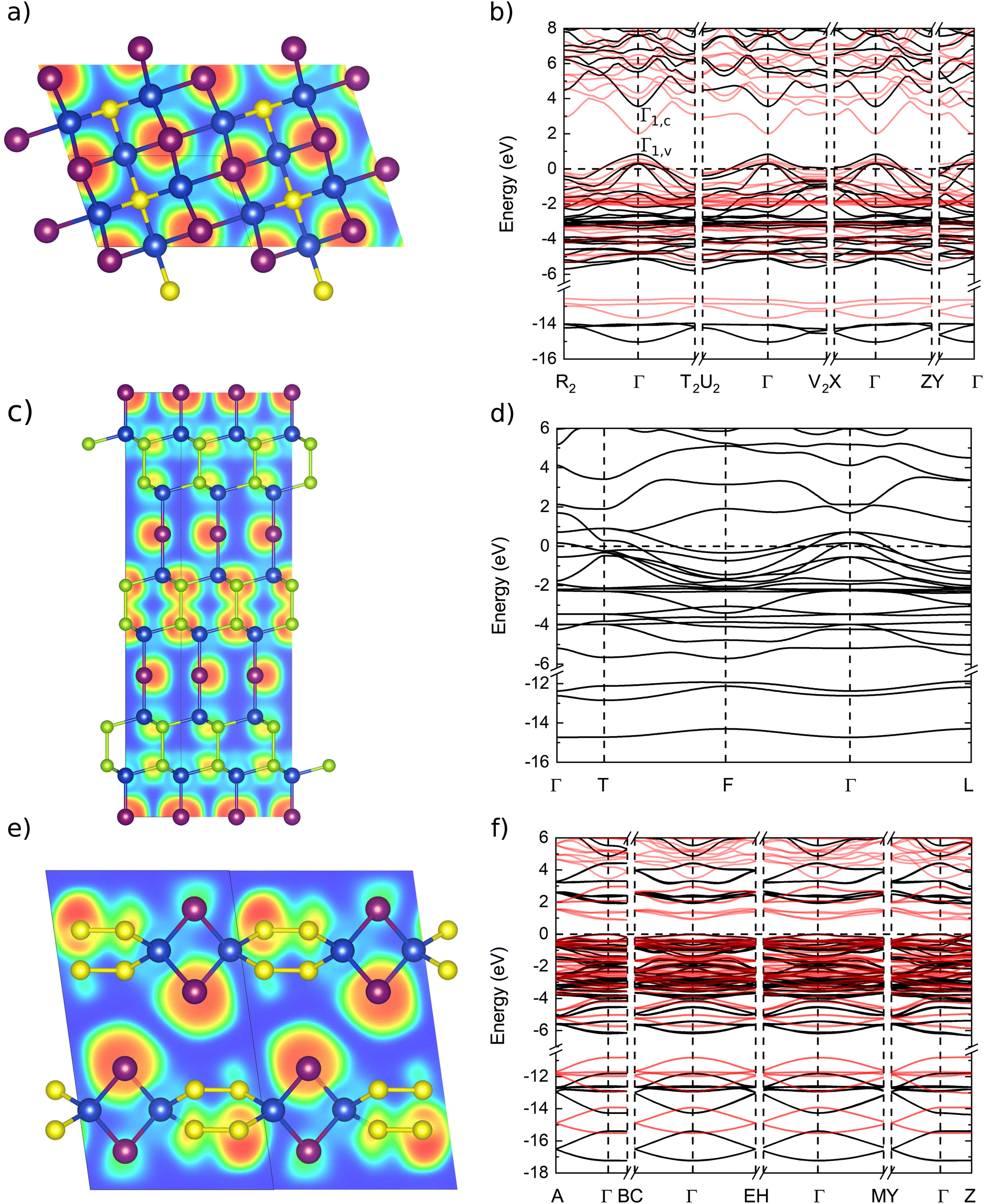 | ||
| Fig. 2 Comparison of crystal structures and band structures for 3 different families of ternary compounds: panels (a) and (b) show Cu3SI2, an example of zinc blende-type ordered alloy, in panels (c) and (d) we find the topological semimetal Cu2Se2I and in panels (e) and (f) a Cu-poor indirect semiconductor with chalcogen–chalcogen bonds, CuS2I. The figures in panels (a), (c) and (e) show the crystal structures together with the electron-localisation function (ELF) and are produced using VESTA,73 while panels (b), (d) and (f) present the corresponding band structures. The band structures are calculated using the modified HSE06 functional (black lines) and PBE (red lines), for the topological semimetal only the PBE band structure is shown. | ||
We find then four p-type degenerate semiconductors with 50% Cu content: Cu3SI2, Cu2SI, Cu3SeI2 and Cu2SeI (a brief description of the properties of these compounds is outlined in the ESI†). These structures are interesting as they intrinsically possess p-type character, as their Fermi energy EF is a few hundred meV below the maximum of the upper valence band. We call this here still a valence band, as it is separated from the other higher energy states by an energy gap and the overall band structure is distinctive of a p-type degenerate semiconductor. To avoid misunderstanding, in Fig. 4, Fig. 2 and Fig. S5 of the ESI,† we added also the symmetry labels of the band maximum (v) and minimum (c) forming a band gap at Γ, reminiscent of the semiconducting band gap of γ-CuI. Even if this band gap is now separating conduction states, its presence is essential to forbid optical transitions for light frequencies in the visible spectrum.
We remark that supercells including Cu vacancies or S,Se substitutions, built on an underlying zinc blende lattice, lead to very similar band structures to the ones depicted in Fig. 2(b). We can, for example, compare the band structure of Fig. 2(b), with those of Cu4I5 and Cu3I4 in ref. 37. This is not surprising as both Cu vacancies and S, Se substitutions on the I site act as acceptor defects, pushing down the Fermi energy from its position in the middle of the gap of semiconducting γ-CuI. The nature of p-type conductivity in these related systems is therefore similar: holes at the top valence of Cu-poor binaries are generated by ordered Cu vacancy complexes,37 while in Cu–I-based ternaries by the ordered S or Se substitutions on the I site. When we are in the alloying regime of compositions, far from the limit of isolated dopants, the Fermi energy is moved deep (0.6–0.8 eV, see Table 4) inside the valence band of the underlying CuI.
We can expect to have in real samples, at finite temperature, disordered configurations of chalcogen atoms on the anion lattice sites, as such a situation will be favoured by entropic effects. The formation of disordered alloys with an underlying zinc blende structure is consequently the most likely situation. The compositions that we explore in this work are limited by the small size of the unit cells. It is however likely that disordered Cu(I,S) and Cu(I,Se) alloys with a zinc blende structure can exist in a larger composition range along the line of the phase diagram connecting CuI and CuS/CuSe. The ratio between the content of chalcogen impurity and the content of iodine, moving from the doping limit to the alloy regime, can therefore be used to determine the position of the Fermi energy (and the resulting hole concentration). In practice, the interplay between Cu vacancies and S, Se substitutions on the I site will contribute together to p-type conductivity, determining the position of the chemical potential.
The energy distances between the VBM and conduction band minimum (CBM) (i.e. the energetic difference Γ1,c − Γ2,v for Cu2SI, Cu2SeI, Cu3SeI2 and Γ1,c − Γ1,v for Cu3SI2) obtained from modified HSE06 calculations are larger than 2.6 eV (only Cu3SeI2 has a smaller energetic gap of 2.2 eV), yielding a clear indication of satisfying transparency in the visible spectrum. The distance of the CBM (i.e. Γ2,c for Cu2SI, Cu2SeI, Cu3SeI2 and Γ1,c for Cu3SI2) and the Fermi level is in all cases larger than the band gap of γ-CuI. The suitability of these ternaries as transparent semiconductors largely depends on how deep the Fermi level EF lies inside the valence band, and therefore on the impact of intravalence transitions on the absorption spectrum. In view of applications, one has to search for a compromise between the thickness of the ternary layer (that will determine light absorption) and the exact I/chalcogen ratio (that will determine the concentration of holes and the position of the Fermi energy in the gap).
We can gather in a different family, finally, three indirect semiconductors with a Cu content lower than 50% and chalcogen–chalcogen bonds: CuSe3I, CuS2I and CuSe2I. The band structure of CuS2I is shown in panel (f) of Fig. 2 as an example. Note that the PBE value of the direct and indirect band gaps of CuSe2I are the same in Table 4 because the difference is smaller than the number of significant digits. The value of the band gap of these ternary compounds is always smaller than the gap of CuI. Only CuSe3I with its direct band gap of 2.5 eV (calculated with modified HSE06) can be expected to be transparent at least for most of the visible spectrum.
We calculated the effective masses of the stable semiconducting materials. Especially important are the effective masses at the top of the valence band, as this quantity is inversely proportional to the mobility of positive charge carriers. In Table 4 we list the smallest light-hole effective masses found, as well as the corresponding direction in the Brillouin zone. The effective masses might depend strongly on the direction, especially for the layered systems. Therefore, to decide if it is worth further considering the material as a p-type TCM or not, the best-obtained value is displayed here. CuSe3I has a hole effective mass that is significantly larger than 1, indicating low mobility for positive charge carriers, and can therefore be discarded. The other materials have effective masses below 1 so high mobilities for positive charge carriers may be possible. Additional effective masses in other directions for candidate p-type TCMs are shown in Table S2 of the ESI.† The best effective mass is obtained for Cu3SeI (0.15me, better than for γ-CuI).
4 Discussion
If we consider all materials on the convex hull, or at a distance from it of less than 30 meV per atom (i.e., approximately the thermal energy at room temperature), from the analysis of Section 3.2 we can subdivide them into three families of systems with similar structural and electronic properties. We have identified for this purpose the following groups: (1) zinc blende-type ordered alloys, where S or Se atoms replace a fraction of I atoms on the anion site; (2) topological semimetals similar to the R![[3 with combining macron]](https://www.rsc.org/images/entities/char_0033_0304.gif) m phase of CuI;79,80 (3) indirect band-gap semiconductors with chalcogen–chalcogen bonds; (4) miscellaneous structures.
m phase of CuI;79,80 (3) indirect band-gap semiconductors with chalcogen–chalcogen bonds; (4) miscellaneous structures.
4.1 Zinc blende-type ordered alloys
We characterize further the electronic band structure, as well as transport and optical properties of Cu2SI, Cu2SeI and Cu3SI2. These crystalline systems are p-type degenerate semiconductors with a good transparency window, as the CBM is 2.6 eV above the Fermi energy, and 3.9 eV above the VBM for Cu2SI, 2.8 eV above the Fermi energy and 3.5 eV the VBM for Cu2SeI and 2.8 eV above the Fermi energy and 3.6 eV above the VBM for Cu3SI2. Moreover, the effective masses are small close to the Fermi level. These properties are inherited from pristine CuI: the band structures are in fact very similar, except for the shift of the chemical potential down inside the valence band. We can see from the values of δX, representing the projection of the wavefunction at the VBM (i.e. Γ1,v for Cu3SI2 and Γ2,v for Cu2SI and Cu2SeI) on atomic orbitals of the chemical element X, reported in Table 4, that a strong p–d-hybridisation between the Cu 3d and I 5p orbitals characterizes these zinc blende phases, as well as the parent γ-CuI crystal.12,46,78 This property is known to be important—together with other factors, like the atomic coordination—to obtain a strong band dispersion at the top of the valence band.16 We further note that the four-fold coordination of Cu and I (or the chalcogen atom), as in γ-CuI, is always preserved in these zinc blende-type structures.The zinc blende-like phase of Cu3SI2 is an ordered alloy with composition CuS1/3I2/3 that lies on the convex hull and presents a metallic band structure, with Fermi energy at a distance of 0.8 eV below the maximum of the highest occupied band. We show the electron localization function (ELF) of Cu3SI2 in Fig. 2. The electrons are, as expected, mainly localized around the anions. A crucial open question concerns the transparency of this phase. The band structures calculated with the PBE and the modified HSE06 functionals are shown in Fig. 2. As already discussed, we can recognize the presence of a band gap between conduction bands, or if we consider this band structure as a modification by alloying of the γ-CuI band structure, we could say that the Fermi level is pushed down so that it is now inside the valence band of CuI. We expect therefore light absorption at low frequencies due to intravalence transitions. For modified HSE06 calculations, we see that the Γ1,c − Γ1,v gap for Cu3SI2, the and Γ1,c − Γ2,v gaps for Cu2SI and Cu2SeI increase significantly, while the difference between Fermi level and VBM (i.e. Γ1,v for Cu3SI2 and Γ2,v for Cu2SI and Cu2SeI) is slightly increased. We calculated the dielectric function of Cu3SI2 and we show it in Fig. 3(a). We can observe at low frequencies, as expected, a Drude-like peak that extends into the visible part of the light spectrum. We conclude that better doping control is necessary to push up the Fermi energy and decrease the metallic character of this material. This can be obtained by reducing the chalcogen fractional content in the alloy, or by compensating n-type doping, e.g. using donor atoms on the Cu-site.32
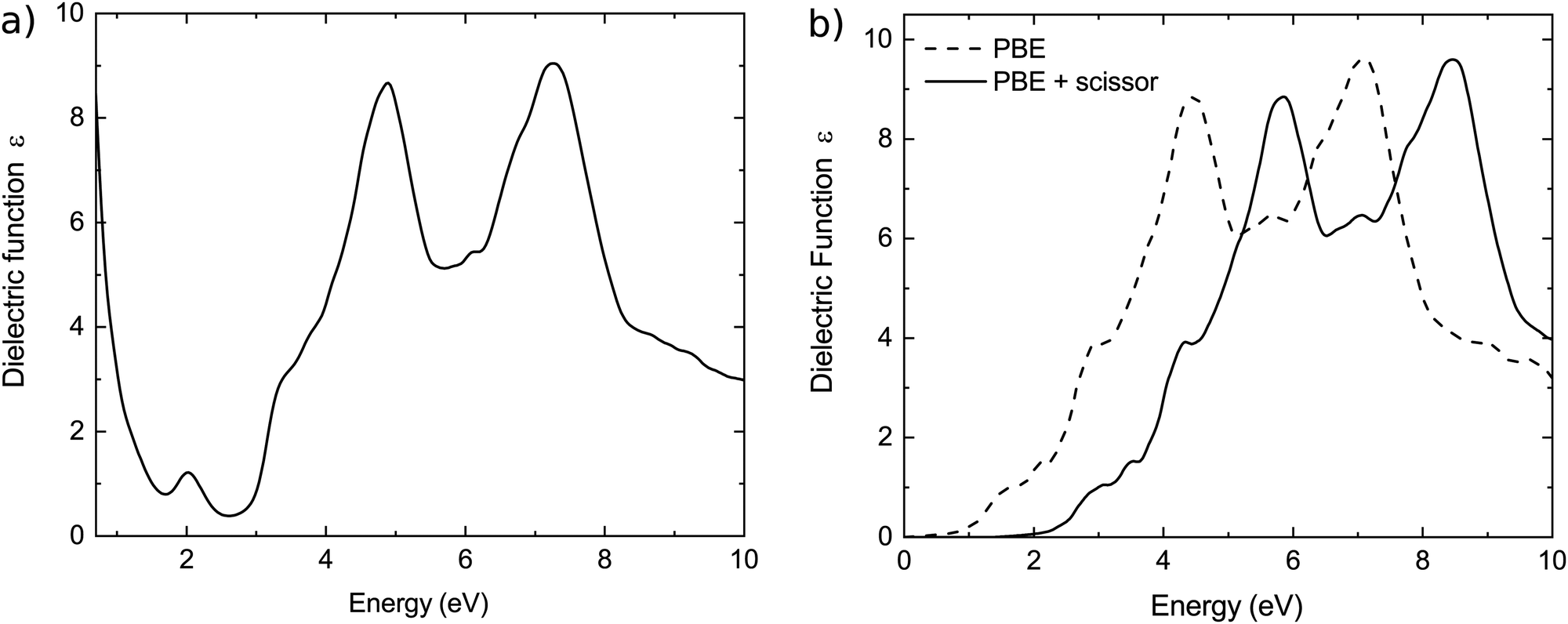 | ||
| Fig. 3 (a) Averaged imaginary part of the dielectric function of undoped Cu3SI2, (b) dielectric function of Cu3SI2 doped with one additional electron per unit cell. A scissor was applied to the PBE band structure to match the modified HSE06 gap. | ||
To illustrate the effect of possible compensating doping we added in Fig. 3(b) an electron per unit cell. We see that the absorption at low frequencies is suppressed as a consequence of the shift towards higher energies of the Fermi level. If we calculate the absorption spectrum using the modified HSE06 band structure, we see that the ternary compound displays the desired transparency in the visible range, provided that the acceptor doping is partially compensated.
We remind that S-doping of CuI was experimentally realized41 and CuI, CuS and Cu3SI2 are all zinc blende-type structures on the convex hull. Furthermore, an ordered zinc blende-type phase of Cu2SI is very close to the hull. We are confident that the fabrication of a CuSxI1−x alloy should be possible over a wide range. This means that the hole densities should be highly tunable.
To further assess the suitability of zinc blende-type Cu(S,Se)I alloys as p-type TCMs, we calculated their transport properties in the CRTA to the Boltzmann equation at 300 K using the AMSET code.71 In Table 5 we provide averaged mobilities per relaxation time (μh/τ) and conductivities per relaxation time (σ/τ) for four structures (three zinc blende-type ternary compounds and a direct-gap material Cu3SeI2 classified as “miscellaneous”), as well as for γ-CuI. The values for γ-CuI were calculated with both CRTA and MRTA (the latter approximation treats various scattering mechanisms explicitly and should be applied in AMSET only to semiconductors). The value of μh/τ for all new structures is smaller by 50–60% than the value for γ-CuI, in agreement with the observation that the hole effective masses of the ternaries are two to three times larger than the one of γ-CuI (see Table 4 and Table S2 of the ESI†). On the other hand, the conductivities (σ/τ) of the four compounds are several orders of magnitude larger than that of doped γ-CuI, owing to the larger concentration of free carriers.
| Composition | Method | (Effective) hole density (cm−3) | τ (fs) | μ h/τ (1011 m2 V−1 s−2) | σ/τ (1020 Sm−1 s−1) |
|---|---|---|---|---|---|
| a Effective hole density calculated from the density of states and the distance of the Fermi level EF to the valence band maximum. b Average of the band- and k-dependent relaxation times from the MRTA calculation. All calculations are performed using the PBEsol exchange–correlation functional. Note that the underestimation of the band gap in PBEsol is not affecting the precision of these results as the Fermi level is inside the valence band of these degenerate semiconductors. | |||||
| Cu3SI2 | CRTA | 7.2 × 10²¹![[thin space (1/6-em)]](https://www.rsc.org/images/entities/char_2009.gif) a a |
10 | 1.13 | 1.31 |
| Cu2SI | CRTA | 1.2 × 10²²a |
10 | 1.05 | 2.02 |
| Cu3SeI2 | CRTA | 6.95 × 10²¹a |
10 | 0.89 | 0.99 |
| Cu2SeI | CRTA | 1.1 × 10²²a |
10 | 1.34 | 2.36 |
| γ-CuI | MRTA | 1 × 10¹⁶ | 17.01b | 2.62 | 4.2 × 10⁻⁶ |
| CRTA | 1 × 10¹⁶ | 10 | 2.55 | 4.08 × 10⁻⁶ | |
| MRTAa | 1 × 10²⁰ | 10.51b | 2.17 | 0.03 | |
| CRTA | 1 × 10²⁰ | 10 | 2.47 | 0.04 | |
4.2 Topological semimetals
We continue by discussing the unusual electronic properties of the structures belonging to the family of topological semimetals: Cu2Se2I and Cu2S2I. These crystals do not possess any complete band gap close to the Fermi level. The atomic structures of the two compounds resemble closely that of the Rm phase of CuI.79,80 We present all three structures in Fig. 4 for an easy comparison. Although Cu2Se2I and Cu2S2I look very similar, they do not belong to the same space group (SG). Cu2Se2I has the trigonal SG 166 (like the Rm phase of CuI) and Cu2S2I has the hexagonal SG 187. One of the key differences between the electronic band structures of these two compounds is the presence of inversion symmetry in Cu2Se2I (SG 166) and its absence in Cu2S2I (SG 187).
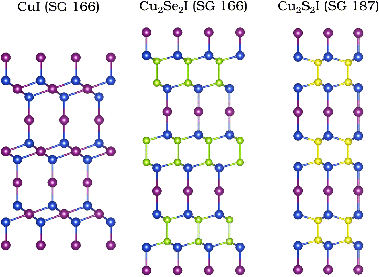 | ||
| Fig. 4 Atomic structures of CuI (SG 166),79,80 Cu2Se2I (SG 166), and Cu2S2I (SG 187). | ||
The Rm phase of CuI has previously been identified as a Dirac semimetal with Dirac points located on the Γ–T line at the Fermi level.80‡ Cu2Se2I has the same SG as CuI and is a metal: we expect hence that it possibly exhibits similar features in its electronic band structure shown in Fig. 5. Indeed, without the inclusion of spin–orbit coupling (SOC) we find a band crossing along the Γ–T line ∼1.0 eV above the Fermi level. We used the IrRep code81 and the Bilbao Crystallographic Server82 to identify the irreducible representation (IRREPs) of the bands of interest along the Γ–T line in the Brillouin zone (BZ). As it can be seen in the central panel of Fig. 5, without considering SOC, the twofold degenerate Λ3 band crosses the nondegenerate Λ1 band. An avoided crossing of the two bands is not possible due to their different IRREPs along Γ–T. After the inclusion of SOC, the Λ3 band splits into the twofold degenerate ![[capital Lambda, Greek, macron]](https://www.rsc.org/images/entities/char_e0bb.gif) 6 and 4 + 5 bands, whereas the Λ1 IRREP becomes 6 (twofold degenerate). The crossing of the 6 and 4 + 5 bands is thus protected by the symmetry of the Γ–T line. Both bands are doubly degenerate (due to the presence of inversion symmetry in the SG 166) and the crossing is thus a Dirac point.
6 and 4 + 5 bands, whereas the Λ1 IRREP becomes 6 (twofold degenerate). The crossing of the 6 and 4 + 5 bands is thus protected by the symmetry of the Γ–T line. Both bands are doubly degenerate (due to the presence of inversion symmetry in the SG 166) and the crossing is thus a Dirac point.
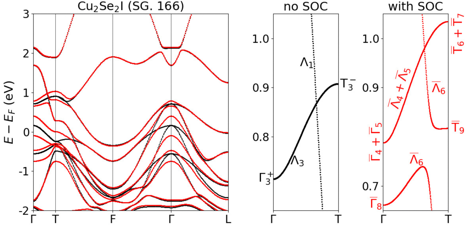 | ||
| Fig. 5 Electronic band structure of Cu2Se2I without SOC (black) and with SOC (red). The bands are calculated using the PBE XC functional. | ||
Cu2S2I crystallizes in the hexagonal SG 187. This symmetry group is similar to SG 166 but it does not have inversion symmetry. We present the electronic band structure of Cu2S2I in Fig. 6. As in the case of Cu2Se2I, there is a band crossing along k = (0, 0, kz) which is the Γ–A line in the BZ of SG 187. Without the inclusion of SOC, we observe that the twofold degenerate Δ3 band crosses the nondegenerate Δ1 band, similarly to the previous case of Cu2Se2I. When SOC is switched on, the Δ1 IRREP becomes ![[capital Delta, Greek, macron]](https://www.rsc.org/images/entities/char_e135.gif) 6 (twofold degenerate). Interestingly, the Δ3 band splits into the twofold degenerate 6 band and the nondegenerate 4 and 5 bands. The presence of nondegenerate bands in materials with time-reversal symmetry is possible only when inversion symmetry is broken, as is the case of SG 187. The Γ–A line in Cu2S2I thus features crossings of twofold degenerate bands with nondegenerate bands. Such crossings are called triple points83 and their presence is protected by the symmetry of the material, similarly to the case of Dirac points.
6 (twofold degenerate). Interestingly, the Δ3 band splits into the twofold degenerate 6 band and the nondegenerate 4 and 5 bands. The presence of nondegenerate bands in materials with time-reversal symmetry is possible only when inversion symmetry is broken, as is the case of SG 187. The Γ–A line in Cu2S2I thus features crossings of twofold degenerate bands with nondegenerate bands. Such crossings are called triple points83 and their presence is protected by the symmetry of the material, similarly to the case of Dirac points.
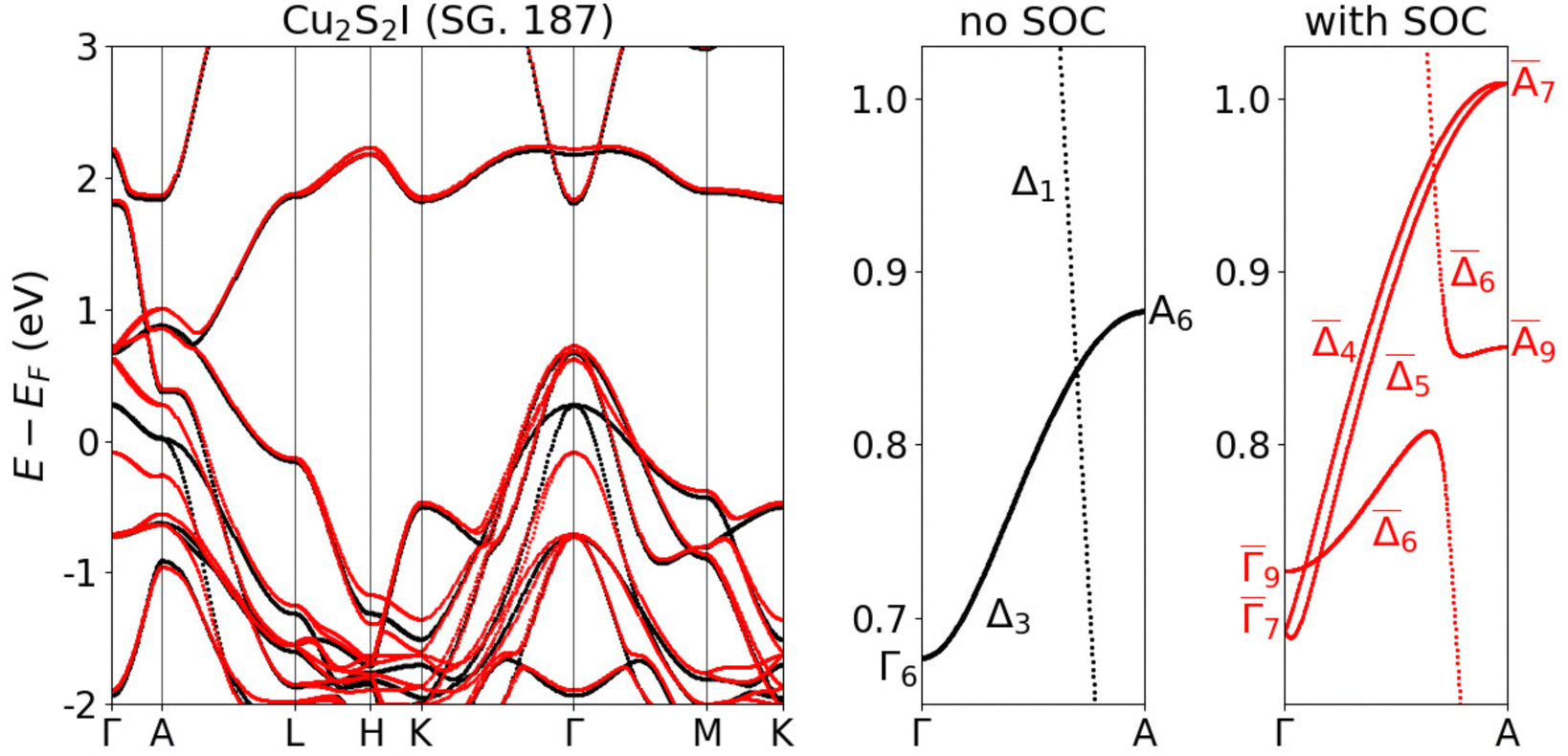 | ||
| Fig. 6 Electronic band structure of Cu2S2I calculated without SOC (black) and with SOC (red). The bands are calculated with the PBE XC functional. | ||
We further confirmed the “enforced semimetal” character of the studied bands of both materials by using the “Check Topologigal Mat”. feature of the Bilbao Crystallographic Server.84 The trace.txt files including the characters of the IRREPs were obtained with the IrRep code81 and they are provided as part of the ESI.†
While the Rm phase of CuI is a true topological semimetal, with Dirac points at the Fermi level, the symmetry-protected crossings in Cu2Se2I and Cu2S2I are located ∼1 eV above it. Moreover, there are also other electronic bands at the energy of the Dirac- and triple points in Cu2Se2I and Cu2S2I. These bands belong to a small hole pocket around the A point and thus we expect specific transport properties of the crossing points to be visible when the chemical potential is shifted to their energy.
The calculations discussed above were performed using the PBE exchange–correlation functional. The authors of ref. 80 checked that for the Rm phase of CuI HSE03 band structures reduce the magnitude of the band inversion from 0.77 eV to ∼0.1 eV, but the topological Dirac semimetal character of the material remained preserved. We calculated the band structure of Cu2Se2I and Cu2S2I with HSE06 and HSE06 with modified α = 0.32 for comparison. In the case of Cu2Se2I, the band inversion and the Dirac points are preserved with HSE06, but HSE06 with modified α = 0.32 restores the band order and introduces a tiny band gap at T. For Cu2S2I we observe a small gap opening already with HSE06 and its size increases when the mixing α is set to 0.32. The comparison of the band structures obtained with different XC functionals is shown in Fig. S6 of the ESI.†
In conclusion, we found two topological semimetals similar to the Rm phase of CuI which is reported to be a Dirac semimetal.80 However, according to the Materials Project database, the latter CuI phase is 256 meV per atom above the hull,79 and therefore it will be quite a challenge to fabricate this structure. However, as we pointed out, the two phases we discussed here (Cu2Se2I and Cu2S2I) are on or very close to the hull. Thus, the incorporation of Se or S stabilizes the structure considerably. The new phases we predicted here could be a starting point for further investigations on topological CuI-based materials. On the other hand, we emphasize that due to their metallic character, they are not suitable for application as transparent conductors.
4.3 Indirect semiconductors with chalcogen–chalcogen bonds
The third family of Cu–I-based ternaries includes indirect semiconductors with chalcogen–chalcogen bonds. In particular, we present here the unreported ternary phases CuS2I and CuSe2I. Both crystals have an indirect band gap, and a notably smaller band gap than CuI (compare Table 4). They also possess effective masses larger than those of pristine CuI. We can conclude that these systems are not preferable to CuI as p-type transparent conducting materials. The main differences, compared to γ-CuI, are due to the chalcogen–chalcogen bonds, which are of covalent nature. These bonds counteract the strong cation p-anion d hybridisation present in the zinc blende-type structures, as presented in Table 4, which is an important ingredient to determine the band gap size and valence band curvature of CuI.12,16,784.4 Miscellaneous structures
The remaining miscellaneous structures are unsuitable as p-type TCMs, either due to lack of transparency or low hole mobility. It is interesting to describe in more detail Cu3SeI2, which possesses a layered structure. This system is a p-type degenerate semiconductor, but compared to Cu3SI2, the Fermi level is farther below the valence band maximum. As a consequence, compensating doping might be harder to realize. The band structures of the miscellaneous materials can be found in the ESI.† Cu3SeI is a semiconductor with small hole effective masses, but a too small band gap. On the other hand, CuSe3I is a semiconductor with a very large hole effective mass and a clear smaller admixture of d-states at the VBM. These calculations point to the importance of a strong p–d hybridisation for the formation of p-type TCMs as discussed in the literature.5 Summary and conclusions
Our accurate and extensive ab initio calculations provide important insights into the ternary phase diagrams of Cu–S–I and Cu–Se–I. Our analysis reveals 11 ternary phases, 9 of which have not been reported before, that are on or very close to the convex hull of stability. We carefully characterized the electronic properties of these ternary compounds to identify potential p-type transparent conductive materials. Our results indicate that zinc blende-type alloys, where chalcogen atoms partially replace iodine on the anion sublattice, show promise as the most suitable candidates, due to the possibility to easily control the carrier concentration through the Cu/I ratio, compared to pure γ-CuI. A strong p–d-hybridisation is present in all promising ternary compounds. Moreover, we identified Cu2Se2I and Cu2S2I as topological semimetals (not transparent, due to their metallic character), with similar structural and electronic properties to a topological phase of CuI reported in the literature.80 In contrast to the CuI topological phase, these ternary crystals are thermodynamically stable, providing an experimental basis for further investigation of topological CuI-based materials. Our results thus demonstrate that chalcogen alloying can offer new strategies for improving and fine-tuning the electronic properties of copper iodide for practical use in transparent electronics applications.Conflicts of interest
There are no conflicts to declare.Acknowledgements
This work received funding from the Deutsche Forschungsgemeinschaft (DFG) through the research unit FOR 2857 and the projects BO 4280/9-1 and RA 3025/2-1. Computational resources were provided by the Leibniz Supercomputing Centre on SuperMUC (project pn68le). S. B. and T. R. acknowledge funding from the Volkswagen Stiftung (Momentum) through the project “dandelion”.Notes and references
- C. G. Granqvist, Appl. Phys. A: Mater. Sci. Process., 1993, 57, 19 CrossRef
.
- A. Liu, H. Zhu, W.-T. Park, S.-J. Kang, Y. Xu, M.-G. Kim and Y.-Y. Noh, Adv. Mater., 2018, 30, 1802379 CrossRef PubMed
- C. Yang, D. Souchay, M. Kneiß, M. Bogner, M. H. Wei, M. Lorenz, O. Oeckler, G. Benstetter, Y. Q. Fu and M. Grundmann, Nat. Commun., 2017, 8, 16076 CrossRef CAS PubMed
- M. Kateb, S. Safarian, M. Kolahdouz, M. Fathipour and V. Ahamdi, Sol. Energy Mater. Sol. Cells, 2016, 145, 200 CrossRef CAS
- A. Liu, H. Zhu, M.-G. Kim, J. Kim and Y.-Y. Noh, Adv. Sci., 2021, 8, 2100546 CrossRef CAS PubMed
- J. Willis and D. O. Scanlon, J. Mater. Chem. C, 2021, 9, 11995–12009 RSC
- D. Han, Y. Zhang, Y. Cong, W. Yu, X. Zhang and Y. Wang, Sci. Rep., 2016, 6, 38984 CrossRef CAS PubMed
- C. O'Dwyer, M. Szachowicz, G. Visimberga, V. Lavayen, S. B. Newcomb and C. M. S. Torres, Nat. Nanotechnol., 2009, 4, 239–244 CrossRef PubMed
- K. Sakamoto, H. Kuwae, N. Kobayashi, A. Nobori, S. Shoji and J. Mizuno, Sci. Rep., 2018, 8, 2825 CrossRef PubMed
- L. Hu, R. H. Wei, X. W. Tang, W. J. Lu, X. B. Zhu and Y. P. Sun, J. Appl. Phys., 2020, 128, 140902 CrossRef CAS
- A. Liu, H. Zhu and Y.-Y. Noh, Adv. Funct. Mater., 2020, 30, 2002625 CrossRef CAS
- M. Grundmann, F. Schein, M. Lorenz, T. Böntgen, J. Lenzner and H. von Wenckstern, Phys. Status Solidi A, 2013, 210, 1671 CrossRef CAS
- D. Chen, Y. Wang, Z. Lin, J. Huang, X. Chen, D. Pan and F. Huang, Cryst. Growth Des., 2010, 10, 2057 CrossRef CAS
- C. Yang, M. Kneiß, F. Schein, M. Lorenz and M. Grundmann, Sci. Rep., 2016, 6, 21937 CrossRef CAS PubMed
- P. Storm, M. Bar, G. Benndorf, S. Selle, C. Yang, H. von Wenckstern, M. Grundmann and M. Lorenz, APL Mater., 2020, 8, 091115 CrossRef CAS
- B. A. D. Williamson, J. Buckeridge, J. Brown, S. Ansbro, R. G. Palgrave and D. O. Scanlon, Chem. Mater., 2017, 29, 2402–2413 CrossRef CAS
- C. Yang, M. Kneiβ, M. Lorenz and M. Grundmann, Proc. Natl. Acad. Sci. U. S. A., 2016, 113, 12929–12933 CrossRef CAS PubMed
- F.-L. Schein, H. von Wenckstern and M. Grundmann, Appl. Phys. Lett., 2013, 102, 092109 CrossRef
- K. Ding, Q. C. Hu, D. G. Chen, Q. H. Zheng, X. G. Xue and F. Huang, IEEE Electron Device Lett., 2012, 33, 1750–1752 CAS
- J. H. Lee, B. H. Lee, J. Kang, M. Diware, K. Jeon, C. Jeong, S. Y. Lee and K. H. Kim, Nanomaterials, 2021, 11, 1237 CrossRef PubMed
- C.-H. Choi, J. Y. Gorecki, Z. Fang, M. Allen, S. Li, L.-Y. Lin, C.-C. Cheng and C.-H. Chang, J. Mater. Chem. C, 2016, 4, 10309 RSC
- A. Tixier-Mita, S. Ihida, B.-D. Ségard, G. A. Cathcart, T. Takahashi, H. Fujita and H. Toshiyoshi, Jpn. J. Appl. Phys., 2016, 55, 04EA08 CrossRef
- J. Liu, Y. Zhang, C. Liu, M. Peng, A. Yu, J. Kou, W. Liu, J. Zhai and J. Liu, Nanoscale Res. Lett., 2016, 11, 281 CrossRef PubMed
- N. Yamada, Y. Kondo, X. Cao and Y. Nakano, Appl. Mater. Today, 2019, 15, 153–162 CrossRef
- S. Nikitine, Philos. Mag., 1959, 4, 1–31 CrossRef CAS
- D. Ahn and S.-H. Park, Sci. Rep., 2016, 6, 20718 CrossRef CAS PubMed
- S.-D. Baek, D.-K. Kwon, Y. C. Kim and J.-M. Myoung, ACS Appl. Mater. Interfaces, 2020, 12, 6037–6047 CrossRef CAS PubMed
- J. A. Christians, R. C. M. Fung and P. V. Kamat, J. Am. Chem. Soc., 2014, 136, 758 CrossRef CAS PubMed
- Z. Yu and L. Sun, Small Methods, 2018, 2, 1700280 CrossRef
- J. Tsiba Matondo, D. Malouangou Maurice, Q. Chen, L. Bai and M. Guli, Sol. Energy Mater., 2021, 224, 111011 CrossRef CAS
- V. Raj, T. Lu, M. Lockrey, R. Liu, F. Kremer, L. Li, Y. Liu, H. H. Tan and C. Jagadish, ACS Appl. Mater. Interfaces, 2019, 11, 24254–24263 CrossRef CAS PubMed
- M. Graužinytė, S. Botti, M. Marques, S. Goedecker and J. Flores-Livas, Phys. Chem. Chem. Phys., 2019, 21, 18839 RSC
- H.-C. Wang, P. Pistor, M. Marques and S. Botti, J. Mater. Chem. A, 2019, 7, 14705–14711 RSC
- J. Shi, T. Cerqueira, W. Cui, F. Nogueira, S. Botti and M. Marques, Sci. Rep., 2017, 7, 43179 CrossRef PubMed
- J. Wang, J. Li and S. Li, J. Appl. Phys., 2011, 110, 054907 CrossRef
- D. Huang, Y.-J. Zhao, S. Li, C.-S. Li, J.-J. Nie, X.-H. Cai and C.-M. Yao, J. Phys. D: Appl. Phys., 2012, 45, 145102 CrossRef
- S. Jaschik, M. R. G. Marques, M. Seifert, C. Rödl, S. Botti and M. A. L. Marques, Chem. Mater., 2019, 31, 7877 CrossRef CAS
- J. Willis, R. Claes, Q. Zhou, M. Giantomassi, G.-M. Rignanese, G. Hautier and D. Scanlon, Chem. Mater., 2023, 35(21), 8995 CrossRef CAS PubMed
- M. Seifert, M. A. L. Marques and S. Botti, Effects of hole doping on the electronic and optical properties of transparent conducting copper iodide, 2022, https://arxiv.org/abs/2212.10855.
- P. Storm, M. Bar, S. Selle, H. von Wenckstern, M. Grundmann and M. Lorenz, Phys. Status Solidi RRL, 2021, 15, 2100214 CrossRef CAS
- K. Ahn, G. Kim, S.-J. Kim, J. Kim, G.-S. Ryu, P. Lee, B. Ryu, J. Cho, Y.-H. Kim, J. Kang, H. Kim, Y.-Y. Noh and M.-G. Kim, Chem. Mater., 2022, 34, 10517 CrossRef CAS
- A. Jain, S. P. Ong, G. Hautier, W. Chen, W. D. Richards, S. Dacek, S. Cholia, D. Gunter, D. Skinner, G. Ceder and K. A. Persson, APL Mater., 2013, 1, 011002 CrossRef
- M. Amsler and S. Goedecker, J. Chem. Phys., 2010, 133, 224104 CrossRef PubMed
- S. Goedecker, J. Chem. Phys., 2004, 120, 9911–9917 CrossRef CAS PubMed
- N. Yamada, Y. Tanida, H. Murata, T. Kondo and S. Yoshida, Adv. Funct. Mater., 2020, 30, 2003096 CrossRef CAS
- M. Seifert, E. Krüger, M. S. Bar, S. Merker, H. von Wenckstern, H. Krautscheid, M. Grundmann, C. Sturm and S. Botti, Phys. Rev. Mater., 2022, 6, 124601 CrossRef CAS
- E. Krüger, M. Seifert, V. Gottschalch, H. Krautscheid, C. Schnohr, S. Botti, M. Grundmann and C. Sturm, AIP Adv., 2023, 13, 035117 CrossRef
- J. Schmidt, H.-C. Wang, T. F. T. Cerqueira, S. Botti and M. A. L. Marques, Sci. Data, 2022, 9, 64 CrossRef CAS PubMed
- T. D. Huan, M. Amsler, M. A. L. Marques, S. Botti, A. Willand and S. Goedecker, Phys. Rev. Lett., 2013, 110, 135502 CrossRef PubMed
- P. Borlido, A. W. Huran, M. A. L. Marques and S. Botti, Phys. Chem. Chem. Phys., 2020, 22, 8442–8449 RSC
- L. Sun, M. Marques and S. Botti, Nat. Commun., 2021, 12, 811 CrossRef CAS PubMed
- L. Sun, M. A. L. Marques and S. Botti, J. Phys. Chem. C, 2022, 126, 15019–15029 CrossRef CAS
- P. E. Blöchl, Phys. Rev. B: Condens. Matter Mater. Phys., 1994, 50, 17953 CrossRef PubMed
- G. Kresse and J. Furthmüller, Comput. Mater. Sci., 1996, 6, 15 CrossRef CAS
- G. Kresse and D. Joubert, Phys. Rev. B: Condens. Matter Mater. Phys., 1999, 59, 1758–1775 CrossRef CAS
- J. P. Perdew, K. Burke and M. Ernzerhof, Phys. Rev. Lett., 1996, 77, 3865 CrossRef CAS PubMed
- K. R. Talley, C. L. Perkins, D. R. Diercks, G. L. Brennecka and A. Zakutayev, Science, 2021, 374, 1488–1491 CrossRef CAS PubMed
- R. Sarmiento-Pérez, T. F. T. Cerqueira, S. Körbel, S. Botti and M. A. L. Marques, Chem. Mater., 2015, 27, 5957–5963 CrossRef
- J. Schmidt, N. Hoffmann, H.-C. Wang, P. Borlido, P. J. M. A. Carriço, T. F. T. Cerqueira, S. Botti and M. A. L. Marques, Adv. Mater., 2023, 35, 2210788 CrossRef CAS PubMed
- J. P. Perdew, A. Ruzsinszky, G. I. Csonka, O. A. Vydrov, G. E. Scuseria, L. A. Constantin, X. Zhou and K. Burke, Phys. Rev. Lett., 2008, 100, 136406 CrossRef PubMed
- J. Sun, A. Ruzsinszky and J. P. Perdew, Phys. Rev. Lett., 2015, 115, 036402 CrossRef PubMed
- V. Stevanovicć, S. Lany, X. Zhang and A. Zunger, Phys. Rev. B: Condens. Matter Mater. Phys., 2012, 85, 115104 CrossRef
- R. Sarmiento-Pérez, S. Botti and M. A. L. Marques, J. Chem. Theory Comput., 2015, 11, 3844–3850 CrossRef PubMed
- F. Tran, J. Stelzl and P. Blaha, J. Chem. Phys., 2016, 144, 204120 CrossRef PubMed
- C. J. Bartel, A. W. Weimer, S. Lany, C. B. Musgrave and A. M. Holder, npj Comput. Mater., 2019, 5, 4 CrossRef
- Y. Hinuma, G. Pizzi, Y. Kumagai, F. Oba and I. Tanaka, Comput. Mater. Sci., 2017, 128, 140–184 CrossRef CAS
- M. Seifert, M. Kawashima, C. Rödl and S. Botti, J. Mater. Chem. C, 2021, 9, 11284–11291 RSC
- J. Vidal, S. Botti, P. Olsson, J.-F. Guillemoles and L. Reining, Phys. Rev. Lett., 2010, 104, 056401 CrossRef PubMed
- M. van Schilfgaarde, T. Kotani and S. Faleev, Phys. Rev. Lett., 2006, 96, 226402 CrossRef CAS PubMed
- P. Borlido, T. Aull, A. W. Huran, F. Tran, M. A. L. Marques and S. Botti, J. Chem. Theory Comput., 2019, 15, 5069–5079 CrossRef CAS PubMed
- A. M. Ganose, J. Park, A. Faghaninia, R. Woods-Robinson, K. A. Persson and A. Jain, Nat. Commun., 2021, 12, 2222 CrossRef CAS PubMed
- A. M. Ganose and A. Jain, MRS Commun., 2019, 9, 874–881 CrossRef CAS
- K. Momma and F. Izumi, J. Appl. Crystallogr., 2011, 44, 1272 CrossRef CAS
- W. Milius and A. Rabenau, Mater. Res. Bull., 1987, 22, 1493–1497 CrossRef CAS
- R. D. Shannon, Acta Crystallogr., 1976, 32, 751–767 CrossRef
- T. Sakuma, J. Phys. Soc. Jpn., 1988, 57, 565–569 CrossRef CAS
- K. Ritter, S. Eckner, C. Preiß, G. Gurieva, T. Bischoff, E. Welter, S. Botti, S. Schorr and C. S. Schnohr, JPhys Energy, 2020, 2, 035004 CrossRef CAS
- M. Cardona, Phys. Rev., 1963, 129, 69 CrossRef
- https://materialsproject.org/materials/mp-23306, Data retrieved from the Materials Project for CuI (mp-23306) from database version v2022.10.28.
- C. Le, X. Wu, S. Qin, Y. Li, R. Thomale, F.-C. Zhang and J. Hu, Proc. Natl. Acad. Sci. U. S. A., 2018, 115, 8311–8315 CrossRef CAS PubMed
- M. Iraola, J. L. Mañes, B. Bradlyn, M. K. Horton, T. Neupert, M. G. Vergniory and S. S. Tsirkin, Comput. Phys. Commun., 2022, 272, 108226 CrossRef CAS
- L. Elcoro, B. Bradlyn, Z. Wang, M. G. Vergniory, J. Cano, C. Felser, B. A. Bernevig, D. Orobengoa, G. de la Flor and M. I. Aroyo, J. Appl. Crystallogr., 2017, 50, 1457–1477 CrossRef CAS
- Z. Zhu, G. W. Winkler, Q. Wu, J. Li and A. A. Soluyanov, Phys. Rev. X, 2016, 6, 031003 Search PubMed
- M. G. Vergniory, L. Elcoro, C. Felser, N. Regnault, B. A. Bernevig and Z. Wang, Nature, 2019, 566, 480–485 CrossRef CAS PubMed
Footnotes |
| † Electronic supplementary information (ESI) available. See DOI: https://doi.org/10.1039/d4tc00277f |
| ‡ In ref. 80 the point T is denoted as Z. |
| This journal is © The Royal Society of Chemistry 2024 |