
 Open Access Article
 This Open Access Article is licensed under a Creative Commons Attribution-Non Commercial 3.0 Unported Licence
A 0D hybrid lead-free halide with near-unity photoluminescence quantum yield toward multifunctional optoelectronic applications†
Dong-Yang
Li‡
ac,
Huai-Yuan
Kang‡
a,
Yu-Hang
Liu
c,
Jie
Zhang
c,
Cheng-Yang
Yue
a,
Dongpeng
Yan
 *b and
Xiao-Wu
Lei
*a
*b and
Xiao-Wu
Lei
*a
aSchool of Chemistry, Chemical Engineer and Materials, Jining University, Qufu, Shandong 273155, P. R. China. E-mail: xwlei_jnu@163.com
bBeijing Key Laboratory of Energy Conversion and Storage Materials, College of Chemistry, Key Laboratory of Radiopharmaceuticals, Ministry of Education, Beijing Normal University, Beijing 100875, P. R. China. E-mail: yandp@bnu.edu.cn
cSchool of Chemistry and Chemical Engineering, Qufu Normal University, Qufu, Shandong 273165, P. R. China
First published on 6th December 2023
Abstract
Zero-dimensional (0D) hybrid metal halides have emerged as highly efficient luminescent materials, but integrated multifunction in a structural platform remains a significant challenge. Herein, a new hybrid 0D indium halide of (Im-BDMPA)InCl6·H2O was designed as a highly efficient luminescent emitter and X-ray scintillator toward multiple optoelectronic applications. Specifically, it displays strong broadband yellow light emission with near-unity photoluminescence quantum yield (PLQY) through Sb3+ doping, acting as a down-conversion phosphor to fabricate high-performance white light emitting diodes (WLEDs). Benefiting from the high PLQY and negligible self-absorption characteristics, this halide exhibits extraordinary X-ray scintillation performance with a high light yield of 55![[thin space (1/6-em)]](https://www.rsc.org/images/entities/char_2009.gif) 320 photons per MeV, which represents a new scintillator in 0D hybrid indium halides. Further combined merits of a low detection limit (0.0853 μGyair s−1), ultra-high spatial resolution of 17.25 lp per mm and negligible afterglow time (0.48 ms) demonstrate its excellent application prospects in X-ray imaging. In addition, this 0D halide also exhibits reversible luminescence off–on switching toward tribromomethane (TBM) but fails in any other organic solvents with an ultra-low detection limit of 0.1 ppm, acting as a perfect real-time fluorescent probe to detect TBM with ultrahigh sensitivity, selectivity and repeatability. Therefore, this work highlights the multiple optoelectronic applications of 0D hybrid lead-free halides in white LEDs, X-ray scintillation, fluorescence sensors, etc.
320 photons per MeV, which represents a new scintillator in 0D hybrid indium halides. Further combined merits of a low detection limit (0.0853 μGyair s−1), ultra-high spatial resolution of 17.25 lp per mm and negligible afterglow time (0.48 ms) demonstrate its excellent application prospects in X-ray imaging. In addition, this 0D halide also exhibits reversible luminescence off–on switching toward tribromomethane (TBM) but fails in any other organic solvents with an ultra-low detection limit of 0.1 ppm, acting as a perfect real-time fluorescent probe to detect TBM with ultrahigh sensitivity, selectivity and repeatability. Therefore, this work highlights the multiple optoelectronic applications of 0D hybrid lead-free halides in white LEDs, X-ray scintillation, fluorescence sensors, etc.
Introduction
In the past several decades, halide perovskite nanocrystals (PNCs) of CsPbX3 (X = Cl, Br, I) have emerged as new-generation optoelectronic functional materials due to excellent optical and electronic properties including direct bandgaps, high absorption coefficients, low defect densities, long carrier diffusion lengths, etc.1–4 PNCs display excellent photoluminescence (PL) performance with diversified advantages of an adjustable emission wavelength covering the whole visible spectrum, narrow bandwidth, high photoluminescence quantum yield (PLQY), etc.5–8 Therefore, three-dimensional (3D) PNCs have been explored as down-conversion phosphors to fabricate solid-state LED and backlit liquid-crystal display (LCD) devices with high external quantum efficiency and a wide color gamut, respectively.9–11 Since 2018, 3D PNCs have been explored as new a kind of scintillator due to their strong X-ray absorption and conversion ability, which aroused new research interest to explore their application in radiation detection and X-ray imaging.12,13 In addition, the unique crystal structure and dynamic ionic bond nature also endow 3D PNCs with a PL switching phenomenon as fluorescence sensors toward external stimuli.14–16 As a consequence, 3D PNCs possess widely advanced application prospects in LEDs, photovoltaic cells, photodetectors, lasers, scintillators, fluorescent probes, etc.17–19 Despite multiple optoelectronic performances, some inescapable shortcomings (such as spectral instability, toxic Pb2+ ions, low scintillation light yield, irreversible PL switching, etc.) remain, seriously restricting the application prospects of 3D PNCs, which inspire further in-depth research to explore new environmentally friendly perovskite derivatives to overcome these drawbacks.Recently, organic–inorganic hybrid zero-dimensional (0D) metal halide perovskites have attracted tremendous attention as some of the promising candidates of 3D PNCs with comparable optoelectronic properties and superior stabilities.20–23 Indeed, versatile organic species and substantial metal ions (Cu+, Mn2+, Zn2+, In3+, Sb3+, etc.) endow hybrid metal halides with diversified structural architectures and PL properties.24–27 Especially, the intrinsic strong quantum confinement and highly localized electrons result in large exciton bonding energy, giving rise to ultrahigh PLQY even up to near unity for 0D hybrid metal halides. The soft crystal lattice readily vibrates with photo-induced excitons as strong electron–phonon coupling, resulting in largely Stokes-shifted broadband light emission.28,29 As a consequence, these 0D hybrid metal halides can be utilized as down-conversion single-component white light phosphors to fabricate LEDs such as (HMTA)4PbMn0.69Sn0.31Br8, [Bmim]2SbCl5, etc.30,31 More significantly, some 0D hybrid metal halides have been further explored as X-ray scintillators with impressive light yield under X-ray excitation due to high PLQY and large Stokes shift.32,33 For instance, 0D Mn2+ and Cu+ based halides display extraordinary scintillation performance with light yield exceeding 80000 photons per MeV, which is far superior to that of typical 3D CsPbX3 PNCs (∼21000 photons per MeV) and commercial scintillators, such as CsI:Tl (54000 photons per MeV), Gd2O2S:Tb (60000 photons per MeV), etc.34–36 In addition, the softer crystal lattice endows 0D hybrid halides with more opportunities to accommodate or recognize small molecules accompanied by change of luminescence properties, acting as a special fluorescent probe with high selectivity and sensitivity.37 Therefore, 0D hybrid metal halides provide an optimal structural platform to realize highly desirable luminescence performance with multiple state-of-the-art optoelectronic applications.38,39 Undoubtedly, ultra-high PLQY and large Stokes shift are crucial for 0D hybrid halides as either down-conversion phosphors or X-ray scintillators to achieve high luminous efficacy and light yield.
Among these 0D hybrid metal halides, indium based halides are deemed to be some of the most promising light emitters with multiple superiorities including diversified coordination configurations of [InX4]−, [InX5]2− and [InX6]3−, non-toxicity, oxidation resistance ability, etc.40,41 Compared with the instabilities of Sn2+ and Ge2+ halides, low efficiencies of Bi3+ phases, nearly fixed green or red spectral emission of Mn2+ based halides, yellow to orange color of Sb3+ halides and blue emission of Zn2+ halides, 0D In3+-based halides represent some of the most desirable light emitters with multiple advantages including tunable light emissions in the whole visible spectral range, nontoxicity, high emission efficiency, strong oxidation resistance ability, etc.42,43 In addition, some 0D hybrid indium halides have been confirmed to display reversible PL switching toward external chemical stimuli as a fluorescent probe to detect small molecules, such as H2O, methanol, etc.44,45 However, the highest PLQY (<60%) of 0D hybrid indium halides lags far behind those of Mn2+ and Cu+ based halides. More miserably, no 0D hybrid indium halide has been able to act as an X-ray scintillator due to low PLQY up to now. These insufficiencies attract new research attention towards designing a new kind of 0D hybrid indium halide to realize highly efficient photoluminescence and radioluminescence through crystal engineering at the molecular level.
In view of these shortcomings, we focus on this domain to explore highly efficient emissive 0D hybrid indium halides aiming to realize multiple advanced optoelectronic applications, especially for solid-state white LEDs and X-ray scintillation. In this work, we prepared a new 0D hybrid indium halide (Im-BDMPA)InCl6·H2O (Im-BDMPA = 3,3′-iminobis(N,N-dimethylpropylamine)) based on discrete [InCl6]3− octahedra via a facile wet-chemistry or mechanical grinding solid-phase reaction method. Through rational Sb3+ doping, highly efficient broadband yellow PL emission with near-unity PLQY and a large Stokes shift of 1.28 eV is achieved for all states in single-crystal, microparticle and flexible composite films. Unexpectedly, the Sb3+ doped (Im-BDMPA)InCl6·H2O displays extraordinary X-ray scintillation performance with a high light yield of 55320 photons per MeV. Although numerous manganese or cuprous halides have been characterized as scintillators, an indium halide based X-ray scintillator has rarely been reported and Sb3+ doped (Im-BDMPA)InCl6·H2O represents a new example of indium halides. Simultaneously, this 0D hybrid indium halide also represents the first luminescent material acting as a unique fluorescent probe toward TBM with ultrahigh sensitivity, selectivity and repeatability. Overall, this 0D halide showcases multiple optoelectronic applications in white LEDs, X-ray scintillation and fluorescence sensors, which opens a broad application window for 0D hybrid halides as promising luminescent materials.
Results and discussion
Bulk single crystals of (Im-BDMPA)InCl6·H2O were prepared via a typical low-temperature solvothermal reaction method. Based on single crystal X-ray diffraction, the structure of (Im-BDMPA)InCl6·H2O crystallizes in the orthorhombic space group P212121 and composed of discrete [InCl6]3− octahedra surrounded by bulk (Im-BDMPA)3+ cations. All the In3+ ions are surrounded by six Cl− ions in [InCl6]3− octahedra with In–Cl bond distances in the normal range of 2.5009(6)–2.5452(6) Å (Fig. 1a). All the neighboring [InCl6]3− octahedrons are separated by long (Im-BDMPA)3+ cations to form a 0D hydrogen bonding structure at the molecular level (Fig. 1b). The sample purity and high crystalline degree of (Im-BDMPA)InCl6·H2O are revealed by matched experimental and simulated powder X-ray diffraction (PXRD) patterns (Fig. 1c). The distributions of the respective chemical compositions have been checked using energy dispersive X-ray spectroscopy (EDS), elemental mapping images, etc. (Fig. S1† and 1d). Sb3+-doped (Im-BDMPA)InCl6·H2O was synthesized by adding the desired amount of SbCl3 into the original synthesis process of the single indium phase, and the coincident PXRD pattern indicates the same crystal structure (Fig. 1c). The chemical composition and successful Sb doping were further confirmed by EDS and elemental mapping, and the optimized doping concentration of Sb element was determined to be 22% by inductively coupled plasma optical emission spectroscopy (ICP-OES) (Fig. S2† and 1d). Subsequently, high-quality (Im-BDMPA)In0.78Sb0.22Cl6·H2O microcrystals were synthesized as an example through a microwave irradiation assisted mechanical stripping method and finally shows a nearly cubic shape with a particle size less than <5 μm (Fig. 1e). The identical diffraction peaks in the PXRD pattern indicate the high crystalline degree of microcrystals (Fig. S3†). (Im-BDMPA)In0.78Sb0.22Cl6·H2O microcrystals can also be prepared by a solid-phase mechanochemical grinding method from precursor materials within a fast time of 30 s and with 100% yield verified by the same PXRD pattern, providing a facile preparation method for various optoelectronic device engineering (Fig. S4 and S5†).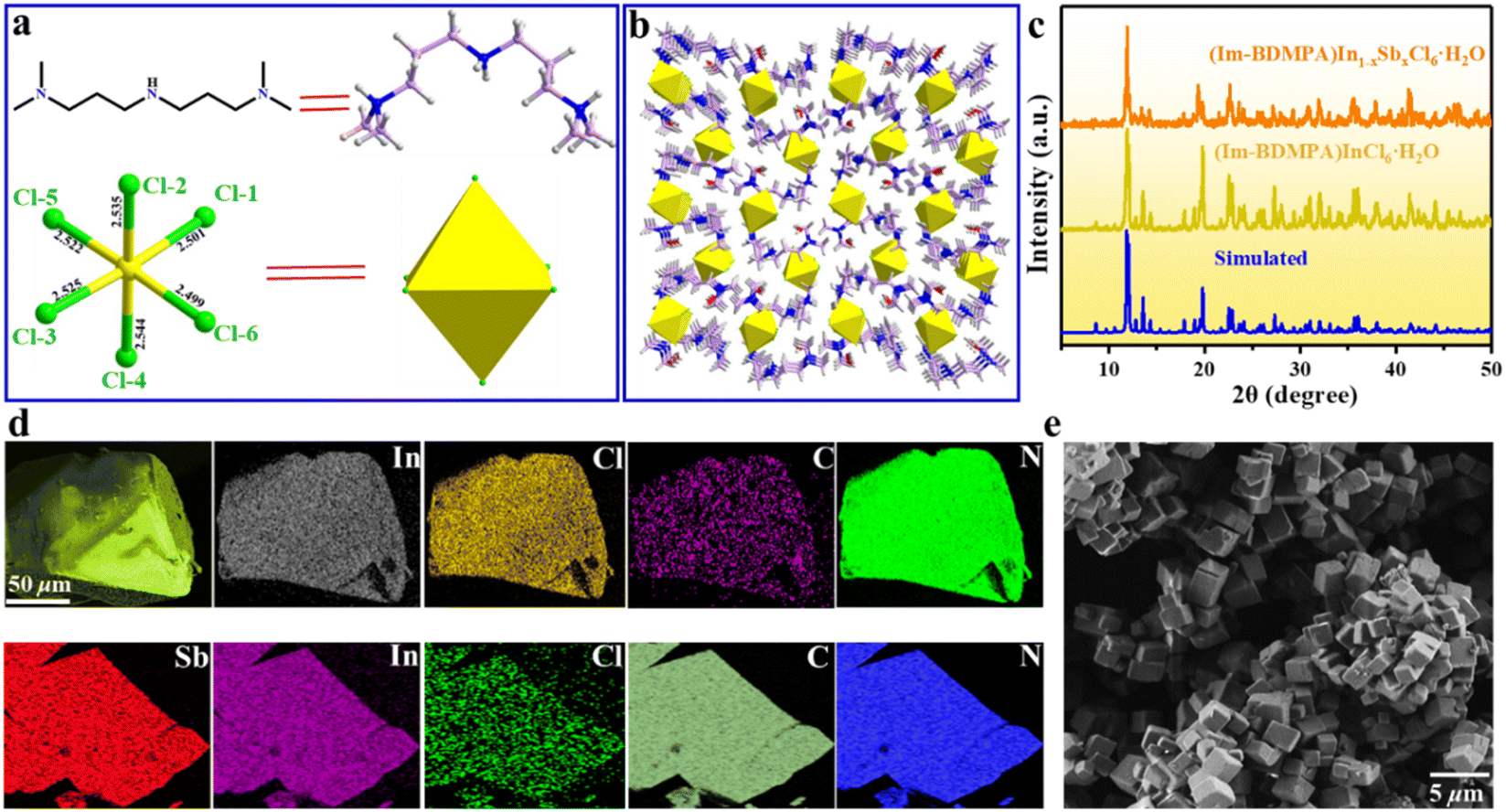 | ||
| Fig. 1 Structural characterization of (Im-BDMPA)In1−xSbxCl6·H2O: (a) (Im-BDMPA)3+ cation and [In/SbCl6]3− octahedron; (b) packing structure of the 0D structure viewed along the a-axis; (c) simulated and experimental PXRD patterns; (d) elemental mapping of SEM images; (e) SEM image of a microparticle. | ||
As shown in Fig. 2a and S6,† bulk single crystals of pristine and doped (Im-BDMPA)InCl6·H2O display the same bright yellow light emission under UV light radiation. The PL properties of (Im-BDMPA)InCl6·H2O are summarized in Fig. S6,† and the doped phases are adopted as an example for discussion with identical luminescence properties. The obtained microcrystals can be well dispersed in ethanol, and the suspension and deposited thin film also emit bright yellow light under UV light (Fig. 2b). The flexible halide/polymer composite film also displays the same yellow luminescence emission (Fig. 2c). Furthermore, the fabricated flexible film depositing on a commercial polyethylene terephthalate (PET) substrate also exhibits bright and stable yellow emission even after bending, indicating its potential application in portable and wearable optoelectronic devices (Fig. S7†). The detailed PL properties were characterized by using absorption, steady state and time-resolved spectroscopy. As shown in Fig. 2d, (Im-BDMPA)In0.78Sb0.22Cl6·H2O exhibits a broad scattering absorption band in the range of about 250–400 nm arising from the electronic transition of 1S0 → 3Pn in 5s2-Sb3+ ions, and the sharp peak at about 220 nm belongs to the interband absorption (Fig. 2d). Notably, the more intensive scattering absorption bands in the lower-energy range than (Im-BDMPA)InCl6·H2O demonstrates the dominance of the contribution from doped Sb3+ ions (Fig. S8†). The PL excitation spectrum covers the whole UV range corresponding to the absorption band, which indicates the coincident electronic transition nature. All the (Im-BDMPA)In1−xSbxCl6·H2O single crystal, microparticle, thin film and flexible composite display the same Gauss-shaped broadband yellow light emissions with a maximum peak at about 570 nm, a large Stokes shift of 291 nm and a wide full-width at half-maximum (FWHM) of 135 nm (Fig. 2d–f).
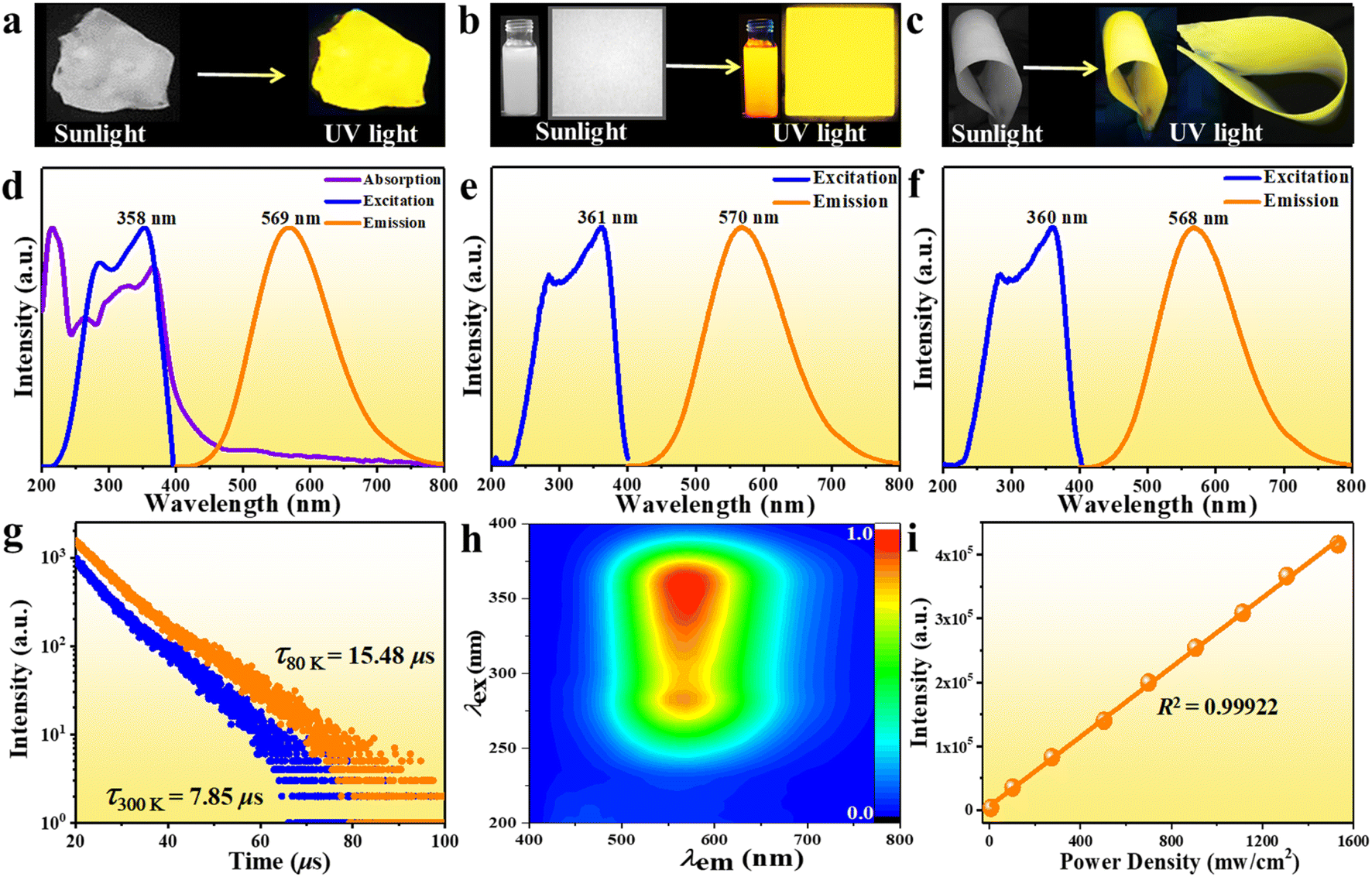 | ||
| Fig. 2 PL characterization of (Im-BDMPA)In0.78Sb0.22Cl6·H2O: (a–c) photo images of bulk crystals, microparticles, the deposited thin film and the flexible composite film under sunlight and 365 nm UV light; (d–f) absorption, excitation and emission spectra of bulk crystals, microparticles and flexible composite; (g) PL decay curves at 300 K and 80 K; (h) 3D consecutive PL map; (i) power density dependent PL emission intensity. | ||
Compared with the low PLQY (48.46%) of pristine indium halide, the Sb3+-doping strategy results in enhanced PLQY up to 95.8% for (Im-BDMPA)In0.78Sb0.22Cl6·H2O, which represents one of the highest values in 0D hybrid Sb3+-doped indium halides (Fig. S9 and Table S1†). The time-resolved PL decay curves give an average lifetime of 7.85 μs (300 K) and 15.48 μs (80 K) based on a double-exponential function, indicating phosphorescence nature (Fig. 2g). The lifetime is slightly longer than those of the undoped precursor (6.35 μs and 12.78 μs), which also indicates that the Sb3+ dopant effectively promotes the radiative recombination rates resulting in higher PLQY (Fig. S6d†). To confirm the PL nature, varied wavelength dependent excitation and emission spectra were recorded in the whole UV-vis spectral light range. The unchanged PL excitation and emission spectral profiles give one dominant emission center in the 3D consecutive PL spectral map, indicating the sole radiative pathway from the single excited state (Fig. 2h, S10 and S11†). In some semiconductors, the broadband emissions maybe derived from the deep or surface defects, and the emission intensity strongly depends on particle size and would be readily quenched by particle aggregation.29 So we compare the PL properties of microscale powders (<10 μm) and bulk single crystals (∼100 μm). The almost identical emission spectral profiles illustrate that the broadband light emissions aren't from the surface defects (Fig. S12†). In addition, the linear dependence relationship between emission intensity and excitation power density further rules out the existence of permanent crystal defect (Fig. 2i and S13†). Similar to previously reported work, the broadband emission with a large Stokes shift, wide FWHM and long lifetime should originate from the radiative recombination of STEs due to the strong electron–phonon (EP) coupling effect in the deformable 0D soft crystal lattice.28,29
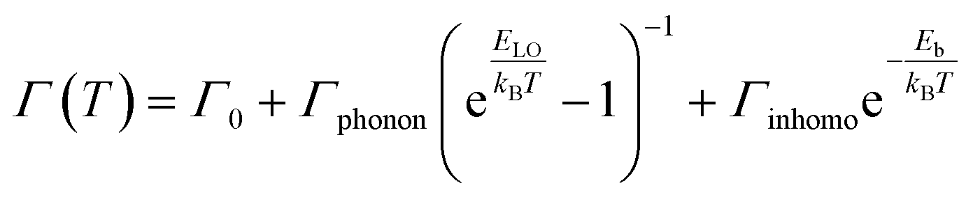
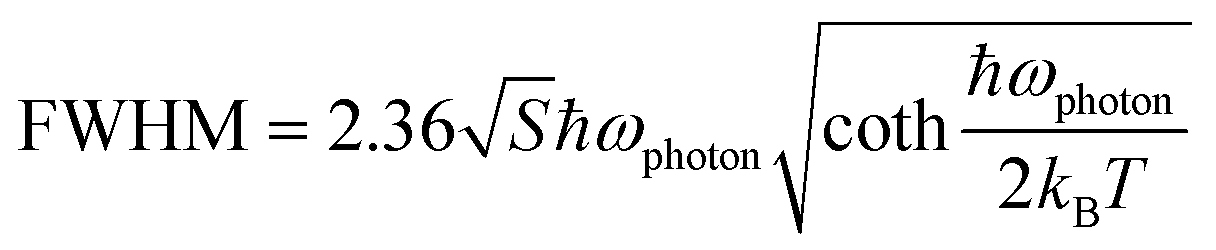
To probe into the underlying PL mechanism and confirm the STE nature, temperature dependent PL emission spectra were recorded from 300 to 80 K (Fig. S14a†). As shown in Fig. 3a, a new weak emission band emerges in the temperature decreasing process, which can be ascribed to be singlet STE. The maximum emission wavelength exhibits a slightly red shift from 558 nm to 570 nm along with the temperature increasing, which is mainly determined by EP interaction based on the theoretical fitting of temperature dependent emission energy evolution (Fig. S14b†). In the temperature decreasing process, the emission intensity increases monotonously from 300 to 80 K owing to decreased thermal quenching and nonradiative recombination rates. Thermal activation energy (Ea) can be extracted by fitting the temperature dependent integrated emission intensity to the Arrhenius equation, which represents the energy barrier of excitons between radiative and nonradiative centers. The calculated Ea of 43 meV is larger than the thermal dissociation energy (∼26 meV) of free excitons at 300 K, indicating the formation of stable bound excitons for (Im-BDMPA)In0.78Sb0.22Cl6·H2O (Fig. 3b). Simultaneously, the emission spectra gradually broaden along with the increasing temperature due to enhanced EP coupling. To accurately evaluate the strength of the EP effect, the temperature dependent FWHM is fitted by using the following equation (1):
 | (1) |
 | (2) |
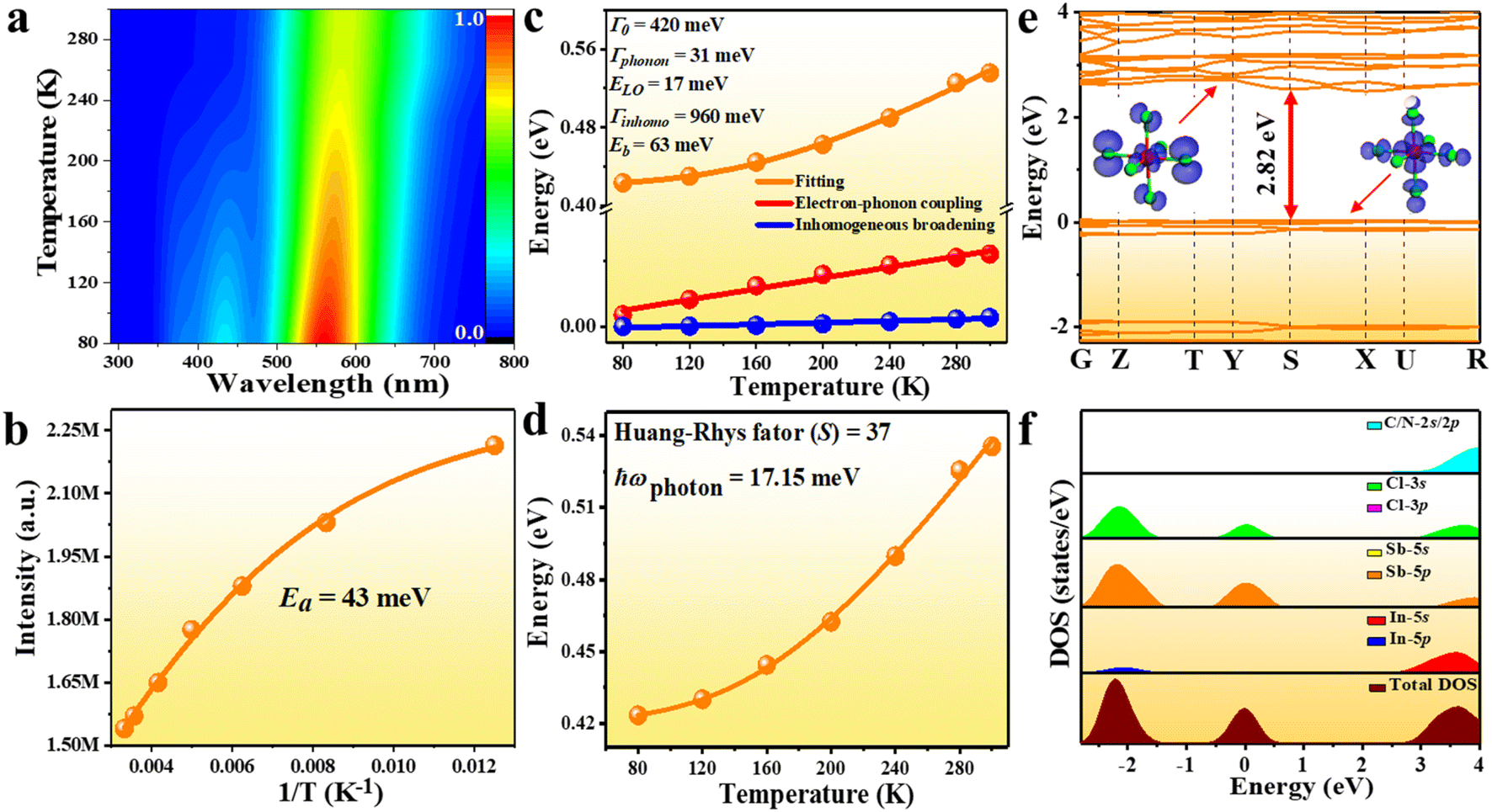 | ||
| Fig. 3 PL mechanism study of (Im-BDMPA)In0.78Sb0.22Cl6·H2O: (a) 3D color mapping of PL emission at varied temperature; (b) experimental and fitted emission intensity vs. reciprocal temperature; (c) temperature-dependent FWHM with the contribution of electron–phonon coupling and inhomogeneous broadening; (d) fitted FWHM according to eqn (2); (e) electronic band structure (inset: electron density maps of the HOMO and LUMO); (f) total and partial densities of states. | ||
Apart from the highly efficient broadband light emission, (Im-BDMPA)In1−xSbxCl6·H2O also exhibits sufficient structural and spectral stability. Based on thermogravimetric analysis, the bulk crystals of (Im-BDMPA)In1−xSbxCl6·H2O can be stable up to about 280 °C (Fig. S17†). Under continuous heating at different temperatures from 80 °C to 280 °C, the PL emission spectral profiles remain unchanged with slightly decreased intensities and PXRD patterns are also fixed indicating sufficient thermal stability (Fig. S18†). After long-term exposure to humid air for one month or strong UV light for 48 h, (Im-BDMPA)In0.78Sb0.22Cl6·H2O retains the high crystalline degree and nearly identical emission intensity (Fig. S19†). Highly efficient and stable broadband (FWHM = 135 nm) yellow light emission motivates us to fabricate a white LED by using (Im-BDMPA)In0.78Sb0.22Cl6·H2O as a down-conversion phosphor. To validate this application, we firstly blend (Im-BDMPA)In0.78Sb0.22Cl6·H2O as a yellow phosphor and commercial BaMgAl10O17:Eu2+ as a blue phosphor with varied ratios. As shown in Fig. 4a and b, the mechanically mixed phosphors display white light emission under irradiation of 365 nm UV light and broadband PL spectra are composed of dual blue-yellow emitting peaks. By finely controlling the blending ratio of the two phosphors, a range of “cold” to “warm” white light can be obtained with tunable correlated color temperature (CCT) from 9520 K to 3320 K (Fig. 4c and Table S2†). Subsequently, a white LED was fabricated as an example by coating the mixed phosphor on an UV chip. Under the drive of 20 mA current, the LED gives bright white light with a CCT of 4590 K and CIE chromaticity coordinates of (0.35, 0.33) (Fig. 4d and e). The obtained color rendering (CRI) index of 95.4 is far higher than that of commercially available white LEDs based on YAG:Ce3+ (CRI < 80).31 To test the reabsorption effect between the two phosphor counterparts, varied electroluminescence (EL) spectra under different operating currents were recorded (Fig. 4f). With the current increasing from 20 mA to 120 mA, both the EL emission intensities of dual emission peaks increase linearly with enhanced drive current without energy transfer between the two phosphors, showcasing potential application in high-power white LEDs. The CIE coordinates, CCT and CRI also keep almost unchanged indicating the negligible self-absorption and efficiency loss of the fabricated white LED (Table S3†). Finally, to evaluate the operating stability of the as-prepared LED, we monitor the EL emission spectra along with operating time under a drive current of 20 mA as shown in Fig. S20.† It can be clearly seen that the EL emission spectra remain unchanged and the luminous efficacy shows no obvious degradation over 100 hours of operation indicating excellent photostability (Fig. 4g).
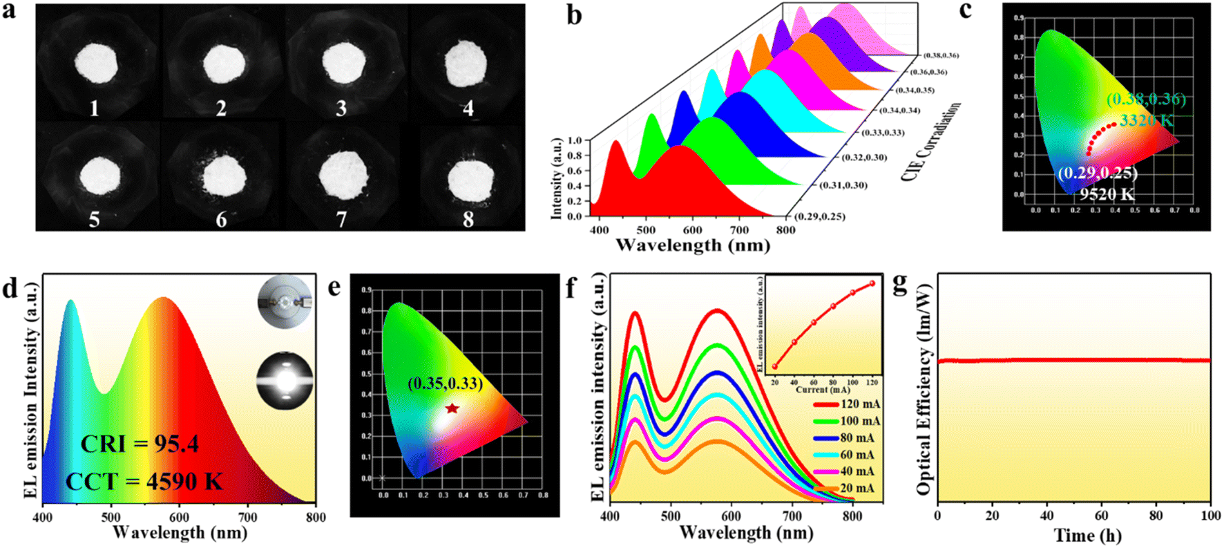 | ||
| Fig. 4 Characterization of a white LED: (a) photo images of mixed phosphors with varying ratios under 365 nm excitation; (b) PL emission spectra and (c) CIE coordinates of mixed phosphors with varying ratios; (d) EL spectrum of the fabricated white LED (inset: photographs of the fabricated WLED with power off and on); (e) CIE coordinates of the white LED; (f) drive current dependent EL emission spectra; (g) current operating time dependent luminous efficiency. | ||
The high PLQY, broad emission band and large Stokes shift demonstrate the potential of (Im-BDMPA)In0.78Sb0.22Cl6·H2O as a promising candidate of X-ray scintillators. We firstly plot the absorption spectra of (Im-BDMPA)In1−xSbxCl6·H2O and commercial Ce:LuAG toward X-ray in a broad range of photon energy based on the photon cross-section database (Fig. S21†). Based on the calculation of the X-ray absorption coefficients (α) versus a broad range of photon energies, the X-ray attenuation efficiencies of (Im-BDMPA)In1−xSbxCl6·H2O are comparable with that of Ce:LuAG in the region of medical digital radiography (18–30 keV). Under the irradiation of 30 kV X-rays, bulk crystals of (Im-BDMPA)In1−xSbxCl6·H2O display bright yellow light as shown in Fig. 5a, and the detailed scintillation properties are further determined by using Ce:LuAG as a standard reference. Both (Im-BDMPA)In1−xSbxCl6·H2O samples display broad radioluminescence (RL) emission bands centered at 570 nm, which are similar to those under UV excitation indicating the same radiative recombination pathway (Fig. 5b). Based on a previous study, the photoelectric effect occurs between the interaction of X-ray phonon and electrons in the inner shell of atoms, generating higher-energy electrons and holes (Fig. 5c). The created hot carriers further lose energy through thermal relaxation into valence and conduction band edges as secondary electrons and holes. Subsequently, the generated electron–hole polarons undergo thermalization to form free excitons (FEs), which transfer to STEs through intersystem crossing to generate broadband emission.12
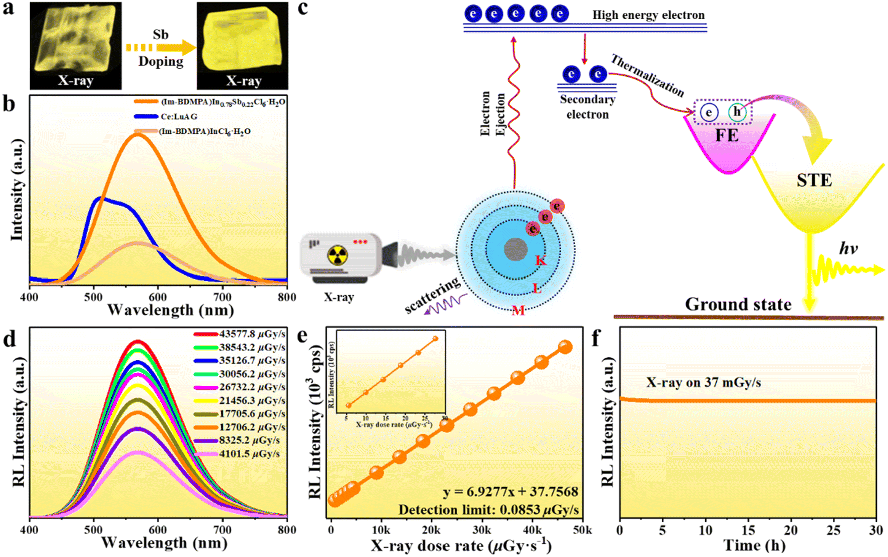 | ||
| Fig. 5 X-ray scintillation performance of (Im-BDMPA)In1−xSbxCl6·H2O: (a) photo images of bulk crystals under X-ray irradiation; (b) RL spectra under 30 kV X-ray excitation; (c) proposed radioluminescence mechanism; (d) X-ray dose rate dependent RL emission spectra; (e) linear dependence of RL emission intensity vs. X-ray dose rate; (f) monitored RL emission intensity under continuous X-ray irradiation. | ||
Although the RL emission intensity of (Im-BDMPA)InCl6·H2O is lower than that of Ce:LuAG, the Sb3+-doped strategy greatly enhances the X-ray response up to about 2.2 times that of Ce:LuAG. By integrating the peak area of RL emission spectra, the light yields of (Im-BDMPA)InCl6·H2O and (Im-BDMPA)In0.78Sb0.22Cl6·H2O are derived to be about 23047 and 55320 photons per MeV on the basis of Ce:LuAG (25000 photons per MeV). Herein, it is noteworthy that (Im-BDMPA)In1−xSbxCl6·H2O represents a rare X-ray scintillator in 0D indium halides, which opens a new window to explore promising candidates for scintillators (Table S4†). Significantly, the light yield of (Im-BDMPA)In0.78Sb0.22Cl6·H2O exceeds that of most of the state-of-the-art commercial scintillators including CsI:Tl (54000 photons per MeV), CsI:Na (41000 photons per MeV), CdWO4 (20000 photons per MeV), LYSO (33200 photons per MeV), etc.35,50–52 Additionally, the scintillation light yield is also superior to those of most halide scintillators, such as 3D CsPbBr3 (∼21000 photons per MeV), (PPN)2SbCl5 (49000 photons per MeV), Cs3MnI5 (33600 photons per MeV), (DIET)3Cu3Br3 (20000 photons per MeV), etc.34,53–55 Such outstanding scintillation performance is related to the high X-ray attenuation efficiency, near unity PLQY and large Stokes shift. To investigate the detection sensitivity of this 0D halide toward X-rays, RL emission spectra were collected at various X-ray dose rates. As shown in Fig. 5d, (Im-BDMPA)In0.78Sb0.22Cl6·H2O displays the same RL emission spectral profiles with monotonously enhanced emission response to the increase of the dose rate from 4101.5 μGy s−1 to 43577.8 μGy s−1. The best linear fitting between RL emission intensity and dose rate gives an ultralow detection limit of 0.0853 μGy s−1 when the signal-to-noise ratio (SNR) is 3, which is much lower than the required value for regular medical diagnostics (5.5 μGy s−1) (Fig. 5e). In addition, the radiant stability against X-ray illumination is also a crucial indicator for evaluating the performance of X-ray scintillators. Under continuous X-ray irradiation at a fixed dose rate of 37 mGy s−1 over 30 hours, the RL emission intensity of (Im-BDMPA)In0.78Sb0.22Cl6·H2O features negligible fluctuation and attenuation demonstrating robust stability for X-rays (Fig. 5f).
Combined superiorities of a high light yield, ultralow detection limit and sufficient X-ray endurance provide the feasibility of applications in X-ray imaging. As a proof of concept, we employed X-ray imaging by using an (Im-BDMPA)In0.78Sb0.22Cl6·H2O based thin screen on a home-made X-ray imaging optical system, and a series of small devices are selected as target objects. As shown in Fig. 6a, an encapsulated fuse tube containing wire was exposed to X-ray illumination, and the different X-ray absorption abilities of the wire and glass tube result in bright spatial intensity contrast, which is translated by the scintillation screen to form optical images with the assistance of a digital camera. Therefore, the inside wire clearly appears in an optical image by using the (Im-BDMPA)In1−xSbxCl6·H2O screen. Similarly, when a ball pen containing metallic spring, metallic device and electronic chip were exposed to X-ray irradiation, all the metallic components can be clearly seen in optical images with an enough contrast ratio on the scintillation screen (Fig. 6b–d).
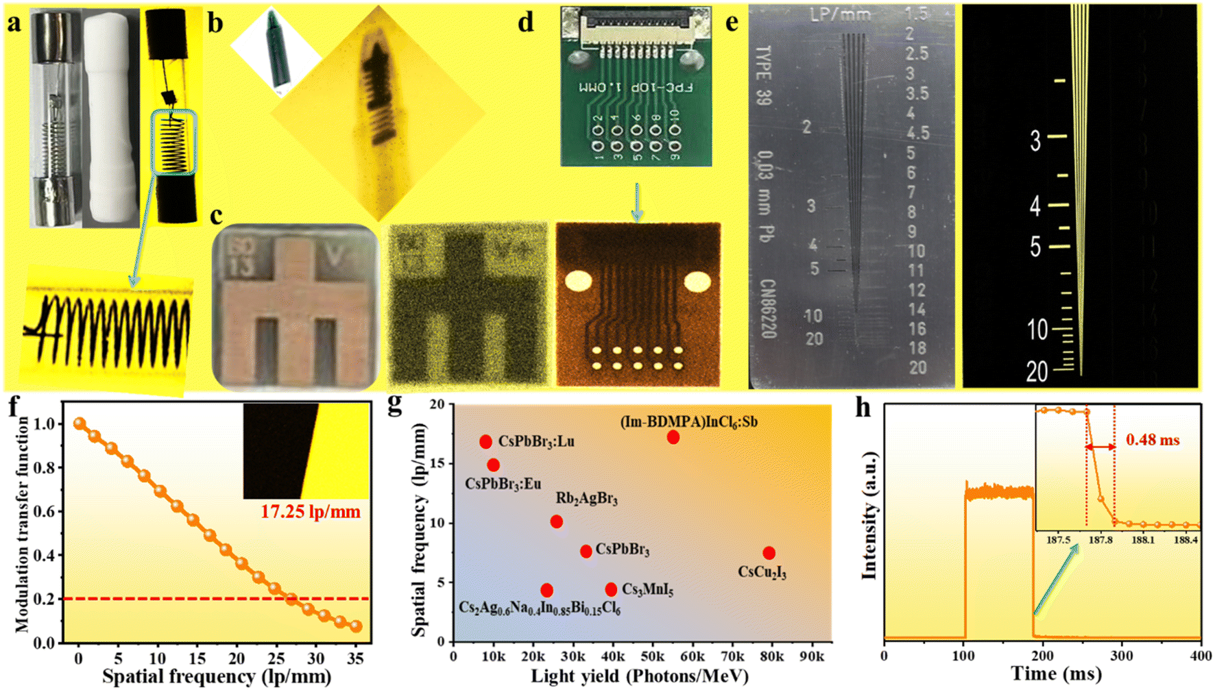 | ||
| Fig. 6 Applications of X-ray imaging based on the (Im-BDMPA)In0.78Sb0.22Cl6·H2O screen under 50 kV X-ray irradiation: photographs and X-ray imaging of (a) an encapsulated fuse tube, (b) ball pen containing metallic spring, (c) metallic device and (d) electronic chip; (e) photograph (left) and X-ray image (right) of the standard X-ray test pattern plate; (f) modulation transfer function (MTF) curve on the X-ray image of a slanted-edge; (g) comparison of the light yield and spatial frequency of metal halide scintillations; (h) X-ray induced afterglow profile. | ||
To obtain the spatial resolution of the scintillation screen, a standard X-ray resolution test pattern plate was adopted to perform the X-ray imaging and the observation limit is almost 20 lp per mm (Fig. 6e). The modulation transfer function (MTF) of the scintillation screen was further employed on the X-ray image of a slanted-edge to obtain more accurate spatial resolution (Fig. 6f). The spatial resolution of the screen is extracted to be 17.25 lp per mm when MFT is equal to 0.2, which is obviously superior to that of commercial CsI(Tl) (10 lp per mm), and metal halide scintillators of CsPbBr3:Lu (16.8 lp per mm), CsPbBr3:Eu (15 lp per mm), BA2PbBr4:10%Mn (10.7 lp per mm), Rb2AgBr3 (10.2 lp per mm), MAPbBr3 (9.8 lp per mm), CsCu2I3 (7.5 lp per mm), etc. (Fig. 6g).35,50,56–61 Finally, considering the fact that a long RL emission lifetime would results in a strong image lag or ghosting after ceasing of X-rays, it is important to test the RL afterglow to evaluate the image contrast.62,63 As shown in Fig. 6h, the emission intensity of the RL afterglow signal rapidly decreases to zero in 0.48 ms after ceasing of X-ray excitation demonstrating high imaging contrast. Overall, the high spatial resolution and negligible afterglow signal indicate the excellent X-ray imaging performance of the (Im-BDMPA)In0.78Sb0.22Cl6·H2O based scintillation screen.
The soft and impressible 0D crystal structure of the halide inspires us to further investigate the external stimulus responsive luminescence switching phenomenon toward various small chemical molecules as a possible fluorescent probe. Herein, we select the (Im-BDMPA)In0.78Sb0.22Cl6·H2O based thin film as a platform to investigate the PL switching performance, which displays the same luminescence as that of bulk crystals but possesses more operability for sensing applications (Fig. 2f). To validate the sensing performance of (Im-BDMPA)In0.78Sb0.22Cl6·H2O, the PL emission spectra were monitored before and after exposing the thin film to various organic solvents over several hours. Herein, a series of small halohydrocarbon molecules or derivatives were selected as sensing targets including chloroacetic acid (CAA), dichloroacetic acid (DCAA), chloropropiophenone (CPP), dibromomethane (DBM), bromodichloromethane (BDCM), dichloromethane (DCM), trichloromethane (TCM), dibromo-monochloro-methane (DBCM) and tribromomethane (TBM). As shown in Fig. 7a, the photo images of the thin film under UV light irradiation reveal that the fluorescence is rapidly quenched by TBM in less than one second, whereas those of others still exhibit the same bright yellow light luminescence. Detailed PL emission spectra demonstrate that the luminescence intensity of the film in TBM solvent are almost completely quenched, whereas those in other organic solvents are nearly unchanged (Fig. 7b and c). To further inspect the sensing selectivity, substantial organic solvents containing different functional groups were selected as contrast targets including alcohol, acetonitrile, acetone, tetrahydrofuran, acetylacetone, aromatic hydrocarbon (e.g., benzene, dimethylbenzene, chlorobenzene, and nitrobenzene), etc. As shown in Fig. S22,† the (Im-BDMPA)In0.78Sb0.22Cl6·H2O films display the same broad yellow emission bands as that of the freshly prepared sample with almost identical emission intensities. These contrast experiments demonstrate that the fluorescence of (Im-BDMPA)In0.78Sb0.22Cl6·H2O is solely quenched by TBM but failed for other organic solvents. More excitedly, the quenched fluorescence of the thin film by TBM can be recovered to the original yellow emission after washing with carbon tetrachloride (CTC), and the PL emission intensity can reach up to nearly 100% of original data (Fig. S23†). To more accurately confirm the repeatability of the reversible quenching–recovering process, we monitor the varied PL emission intensity of the (Im-BDMPA)In0.78Sb0.22Cl6·H2O film during consecutive impregnation-washing cycles. As shown in Fig. 7d, the thin film displays a repeatable PL quenching–recovering cycle and the luminescence is able to persistently return to the original yellow color after washing with CTC even after consecutive 20 cycles. Simultaneously, the negligible decrease of emission intensity also indicates high reversibility and repeatability (Fig. 7e). After exposing to these organic solvents, the PXRD patterns reveal strong diffraction peaks with a high crystalline degree, indicating a stable crystal structure lattice (Fig. S24–S26†). Therefore, (Im-BDMPA)In0.78Sb0.22Cl6·H2O displays reversible TBM responsive fluorescence on/off switching, which indicates the feasibility of the fluorescent probe to detect TBM.
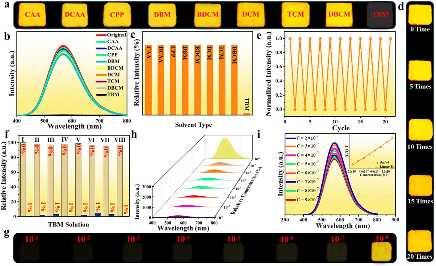 | ||
| Fig. 7 Application of the fluorescent probe: (a) photo images of the film after exposing to various organic solvents; (b) PL emission spectra and (c) normalized emission intensity of the thin film after exposing to organic solvents; (d) photo images and (e) PL emission intensity of the film during quenching–recovering cycles in TBM as a function of cycle number; (f) normalized luminescence intensity histogram of the film after exposed to mixed solutions of TBM and other organic solvents with concentrations of 0% and 1% ((I) CAA; (II) DCAA; (III) CPP; (IV) DBM; (V) BDCM; (VI) DCM; (VII) TCM; (VIII) DBCM); (g) photo images and (h) PL emission spectra of the film after exposing to CTC solutions with low concentrations of TBM from 10−1 to 10−8 by volume; (i) PL emission spectra of the thin film after soaking in CTC solutions with different concentrations of TBM from 2 × 10⁻⁷ to 9 × 10⁻⁷ by volume (inset: linear fitting of emission intensity ratio vs. TBM concentration). | ||
The sharply contrasting response to TBM and other organic solvents inspires us to investigate the selectivity for sensing applications, and a series of anti-interference experiments were performed in mixed solutions of TBM and other halohydrocarbon solvents. As depicted in Fig. S27† and 7f, the PL emission intensities of the film were almost completely quenched after exposing to mixed solutions containing a small amount of TBM (1%) but failed in TBM free solutions, which manifest that (Im-BDMPA)In0.78Sb0.22Cl6·H2O possesses an excellent sensing selectivity toward TBM. The sensitivity of the fluorescent probe is another crucial indicator to evaluate the sensing performance in practical applications. To explore the sensitivity of the fluorescent probe, a series of dilute TBM/CTC solutions with very low concentrations from 10−1 to 10−8 by volume were further blended as representative targets. As shown in Fig. 7g and h, both the photo images and PL emission spectra indicate that the film remains to exhibit the PL quenching phenomenon when the content of TBM is reduced to 10−7 (0.1 ppm). Detailed PL emission spectra toward ultra-dilute TBM/CTC solutions in the concentration range of 2 × 10⁻⁷ to 9 × 10⁻⁷ indicate that the fluorescence intensity of the film gradually decreases with the increase of TBM concentration, and the quenching effect (I0/I − 1) is linearly dependent on the TBM concentration with a good linear relation (R2 = 0.9998), indicating excellent detection operability (Fig. 7i). These results demonstrate that (Im-BDMPA)In0.78Sb0.22Cl6·H2O is a highly desirable fluorescent probe to detect TBM with high selectivity, sensitivity and repeatability.
To illustrate the quenching mechanism toward TBM, the UV-vis absorption spectra were firstly studied on the sample after immersing in various organic solvents. As shown in Fig. S28,† the absorption spectra do not display any change after soaking in most of the organic solvents, while the TBM-treated sample exhibits a more widespread absorption range from 200 nm to 650 nm, which overlaps partially with the emission spectrum of the as-synthesized sample, indicating significant electron exchange and self-absorption characteristics. To further verify the energy transfer between (Im-BDMPA)In0.78Sb0.22Cl6·H2O and TBM, X-ray photoelectron spectroscopy (XPS) was performed at the surface of the sample. Compared with the as-synthesized halide, the binding energies of C-2s and N-2s shift slightly to lower energy, while those of Cl-2p, In-3d and Sb-3d shift to higher energy in the TBM treated halide sample (Fig. S29†). All these investigations indicate the energy transfer between (Im-BDMPA)In0.78Sb0.22Cl6·H2O and TBM molecules, which consume drastically the excited carriers and quench the luminescence of the halide, and a similar phenomenon has been confirmed in numerous fluorescent probes.64
Conclusions
In summary, we herein demonstrate a new 0D hybrid indium/antimony halide as a highly efficient broadband yellow light emitter with near-unity PLQY and multifunctional applications. Firstly, the broadband emission realizes a high-performance white LED with tunable color temperature. Secondly, this halide represents a new X-ray scintillator in 0D hybrid indium halide with promising X-ray imaging applications, as highlighted by the combined merits of a prominent light yield, low detection limit, ultra-high spatial resolution and negligible afterglow time. Thirdly, reversible TBM responsive luminescence off–on switching enables it to be a perfect real-time fluorescent probe to detect TBM with ultrahigh sensitivity, selectivity and repeatability. Therefore, high-performance multiple optoelectronic applications in white LEDs, X-ray scintillation and fluorescence sensors are synchronously realized in a 0D halide structural platform. These multiple applications benefit from the synergistic effects of intrinsic quantum confinement, strong electron–phonon coupling, the sufficient absorption coefficient of X-ray and the impressible structure in the 0D deformable crystal lattice. This work not only deepens the fundamental understanding of the luminescence properties of 0D hybrid halides but also realizes multiple optoelectronic applications. We believe that this research would guide the rational design of new 0D hybrid metal halides as advanced luminescent materials in cutting-edge optoelectronic fields.Data availability
The data that support the finding of this study are available from the corresponding author upon reasonable request.Author contributions
D.-Y. Li and H.-Y. Kang designed the experiments and carried out material synthesis, Y.-H. Liu and J. Zhang assisted in the measurements, Y.-C. Yue helped in data analysis, and D. Yan and X.-W. Lei were responsible for supervision and revising the manuscript. All authors participated in discussing the data and writing the manuscript.Conflicts of interest
The authors declare no conflict of interest.Acknowledgements
We acknowledge the financial support from the National Natural Science Foundation of China (No. 22171105 and 22275021), Shandong Provincial Natural Science Foundation (No. ZR2021MB001, ZR2020KB012 and ZR2022YQ14), Fund of State Key Laboratory of Structural Chemistry (No. 20210015), Beijing Municipal Natural Science Foundation (Grant No. JQ20003) and Special Foundation of Taishan Scholar Project.References
- B. A. Rosales, L. E. Mundt, L. T. Schelhas and L. M. Wheeler, J. Am. Chem. Soc., 2022, 144, 667–672 CrossRef CAS PubMed.
- L. W. Zhang, R. C. Shen, J. Tan and Q. Yuan, Chin. J. Struct. Chem., 2022, 41, 2202148–2202158 CAS.
- X. L. Jing, D. L. Zhou, R. Sun, Y. Zhang, Y. Y. C. Li, X. D. Li, Q. J. Li, H. W. Song and B. B. Liu, Adv. Funct. Mater., 2021, 31, 2100930 CrossRef CAS.
- I. Spanopoulos, I. Hadar, W. J. Ke, P. J. Guo, E. M. Mozur, E. Morgan, S. X. Wang, D. Zheng, S. Y. Padgaonkar, G. N. Reddy, E. A. Weiss, M. C. Hersam, R. Seshadri, R. D. Schaller and M. G. Kanatzidis, J. Am. Chem. Soc., 2021, 143, 7069–7080 CrossRef CAS PubMed.
- H. Kim, J. H. Park, K. Y. Kim, D. Lee, M. Y. Song and J. Park, Adv. Sci., 2022, 9, 2104660 CrossRef CAS.
- X. T. Gao, N. N. Chen, M. L. Cao, Y. Shi and Q. F. Zhang, Chin. J. Struct. Chem., 2022, 41, 2211110–2211116 CAS.
- L. Mao, P. Guo, S. Wang, K. Cheetham and R. Seshadri, J. Am. Chem. Soc., 2020, 142, 13582–13589 CrossRef CAS PubMed.
- F. F. Gao, X. Li, Y. Qin, Z. G. Li, T. M. Guo, Z. Z. Zhang, G. D. Su, C. Y. Jiang, M. Azeem, W. Li, X. Wu and X. H. Bu, Adv. Opt. Mater., 2021, 9, 2100003 CrossRef CAS.
- B. Zhou, G. W. Xiao and D. P. Yan, Adv. Mater., 2021, 33, 2007571 CrossRef CAS PubMed.
- P. S. Lv, L. P. Li, C. Z. Wang, Z. Q. Wu, J. R. Qiu and Y. M. Yang, Laser Photonics Rev., 2022, 16, 2200389 CrossRef CAS.
- Z. Wang, J. T. Mo, J. J. Pan and M. Pan, Adv. Funct. Mater., 2023, 2300021 CrossRef CAS.
- H. D. Wu, Y. S. Ge, G. D. Niu and J. Tang, Matter, 2021, 4, 144–163 CrossRef CAS.
- O. Rabin, J. Grimm, G. Wojtkiewicz and R. Weissleder, Nat. Mater., 2006, 5, 118–122 CrossRef CAS PubMed.
- Y. T. Chen, C. Y. Zhao, T. T. Zhang, X. H. Wu, W. J. Zhang and S. J. Ding, Small, 2021, 17, 2007543 CrossRef CAS.
- S. S. Cai, Y. Y. Ju, Y. M. Wang, X. W. Li, T. Guo, H. Z. Zhong and L. L. Huang, Adv. Sci., 2022, 2104708 CrossRef CAS.
- H. J. Chen, M. Zhang, R. H. Bo, C. Barugkin, J. H. Zheng, Q. S. Ma, S. J. Huang, A. W. Y. Ho-Baillie, K. R. Catchpole and A. Tricoli, Small, 2018, 14, 1702571 CrossRef.
- G. D. Li, J. Song, J. H. Wu, Z. Y. Song, X. B. Wang, W. H. Sun, L. Q. Fan, J. M. Lin, M. L. Huang, Z. Lan and P. Gao, ACS Energy Lett., 2021, 6, 3614–3623 CrossRef CAS.
- Y. F. Sang, L. J. Xu and Z. N. Chen, Chin. J. Struct. Chem., 2022, 41, 2205070–2205076 CAS.
- B. Zhou and D. P. Yan, Angew. Chem., Int. Ed., 2019, 58, 15128–15135 CrossRef CAS.
- M. Li and Z. G. Xia, Chem. Soc. Rev., 2021, 50, 2626–2662 RSC.
- X. Yang, L. Ma and D. Yan, Chem. Sci., 2019, 10, 4567 RSC.
- J. Q. Zhao, H. S. Shi, L. R. Zeng, H. Ge, Y. H. Hou, X. M. Wu, C. Y. Yue and X. W. Lei, Chem. Eng. J., 2022, 431, 134336 CrossRef CAS.
- B. Zhou and D. Yan, Chem. Sci., 2022, 13, 7429 RSC.
- S. G. Zhou, Y. H. Chen, K. L. Li, X. W. Liu, T. Zhang, W. Shen, M. Li, L. Zhou and R. X. He, Chem. Sci., 2023, 14, 5415–5424 RSC.
- F. Jiang, Z. N. Wu, M. Lu, Y. B. Gao, X. Li, X. Bai, Y. Ji and Y. Zhang, Adv. Mater., 2023, 2211088 CrossRef.
- G. Y. Xu, C. Y. Wang, Y. C. Li, W. Meng, G. G. Luo, M. Peng, B. Xu and Z. T. Deng, Chem. Sci., 2023, 14, 5309–5315 RSC.
- Z. S. Xing, Z. C. Zhou, G. H. Zhong, C. S. Chan, Y. Y. Li, X. H. Zou, J. E. Halpert, H. B. Su and K. S. Wong, Adv. Funct. Mater., 2022, 32, 2207638 CrossRef CAS.
- Y. Y. Fang, J. T. Wang, L. Zhang, G. M. Niu, L. Z. Sui, G. R. Wu, K. J. Yuan, K. Wang and B. Zou, Chem. Sci., 2023, 14, 2652–2658 RSC.
- Q. J. Wang, T. X. Bai, S. J. Ji, H. Y. Zhao, X. Meng, R. L. Zhang, J. K. Jiang and F. Liu, Adv. Funct. Mater., 2023, 33, 2303399 CrossRef CAS.
- L. J. Xu, S. J. Lee, X. S. Lin, L. Ledbetter, M. Worku, H. R. Lin, C. K. Zhou, H. Liu, A. Plaviak and B. W. Ma, Angew. Chem., Int. Ed., 2020, 59, 14120–14123 CrossRef CAS PubMed.
- M. Worku, Y. Tian, C. Zhou, S. Lee, Q. Meisner, Y. Zhou and B. Ma, ACS Appl. Mater. Interfaces, 2018, 10, 30051 CrossRef CAS.
- X. Liu, Y. Li, L. Zhou, M. Li, Y. Y. Zhou and R. X. He, Adv. Opt. Mater., 2022, 10, 2200944 CrossRef CAS.
- X. T. Zhang, H. Y. Qiu, W. Luo, K. F. Huang, Y. Chen, J. C. Zhang, B. H. Wang, D. L. Peng, Y. Wang and K. Z. Zheng, Adv. Sci., 2023, 10, 2207004 CrossRef CAS.
- Y. H. Zhang, R. J. Sun, X. Y. Ou, K. F. Fu, Q. S. Chen, Y. C. Ding, L. J. Xu, L. M. Liu, Y. Han, A. V. Malko, X. G. Liu, H. G. Yang, O. M. Bakr, H. Liu and O. F. Mohammed, ACS Nano, 2019, 13, 2520–2525 CrossRef CAS.
- J. J. Ma, W. J. Zhu, L. Lei, D. G. Deng, Y. J. Hua, Y. M. Yang, S. Q. Xu and P. N. Prasad, ACS Appl. Mater. Interfaces, 2021, 13, 44596–44603 CrossRef CAS.
- M. M. Xing, W. H. Cao, T. Pang, X. Q. Ling and N. Chen, Sci. Bull., 2009, 54, 2982–2986 CrossRef CAS.
- T. Huang, Q. L. Wei, W. C. Lin, H. Peng, S. F. Yao and B. S. Zou, Mater. Today Phys., 2022, 25, 100703 CrossRef CAS.
- X. C. Zhang, X. L. Yu, J. Y. Wu and W. G. Huang, Chin. J. Struct. Chem., 2022, 41, 2212001–2212003 CAS.
- S. Q. Sun, M. Lu, X. P. Gao, Z. P. Shi, B. Bai, W. W. Yu and Y. Zhang, Adv. Sci., 2021, 8, 2102689 CrossRef.
- H. Fattal, T. D. Creason, C. J. Delzer, A. Yangui, J. P. Hayward, B. J. Ross, M. H. Du, D. T. Glatzhofer and B. Saparov, Inorg. Chem., 2021, 60, 1045–1054 CrossRef CAS.
- J. H. Wei, J. F. Liao, L. Zhou, J. B. Luo, X. D. Wang and D. B. Kuang, Sci. Adv., 2021, 7, eabg3989 CrossRef CAS.
- J. H. Wei, J. B. Luo, J. F. Liao, W. T. Qu and D. B. Kuang, Sci. China Mater., 2022, 65, 764–772 CrossRef CAS.
- F. Zhang, X. Z. Ji, W. Q. Liang, Y. Li, Z. Z. Ma, M. Wang, Y. Wang, D. Wu, X. Chen, D. W. Yang, X. J. Li, C. X. Shan and Z. F. Shi, Mater. Horiz., 2021, 8, 3432–3442 RSC.
- L. Zhou, J. F. Liao, Z. G. Huang, J. H. Wei, X. D. Wang, W. G. Li, H. Y. Chen, D. B. Kuang and C. Y. Su, Angew. Chem., Int. Ed., 2019, 58, 5277–5281 CrossRef CAS.
- D. Y. Li, J. H. Song, Y. Cheng, X. M. Wu, Y. Y. Wang, C. J. Sun, C. Y. Yue and X. W. Lei, Angew. Chem., Int. Ed., 2022, 61, e202206437 CrossRef CAS.
- A. K. Viswanath, J. I. Lee, D. Kim, C. R. Lee and J. Y. Leem, Phys. Rev. B: Condens. Matter Mater. Phys., 1998, 58, 16333 CrossRef CAS.
- A. M. Kelley, ACS Nano, 2011, 5, 5254–5262 CrossRef CAS.
- Q. Zhang, H. Q. Li, Y. Ma and T. Y. Zhai, Prog. Mater. Sci., 2016, 83, 472–535 CrossRef CAS.
- S. X. Li, Y. Pan, W. M. Wang and Y. Li, Chem. Eng. J., 2022, 434, 134593 CrossRef CAS.
- Z. K. Ye, X. Lin, N. Wang, J. H. Zhou, M. Y. Zhu, H. Y. Qin and X. G. Peng, Nat. Commun., 2021, 12, 4283 CrossRef CAS.
- L. Zhou, K. Zhang, H. Li, W. Shen, N. Li and R. X. He, Adv. Funct. Mater., 2021, 31, 2108561 CrossRef CAS.
- G. F. Carpenter, M. J. Coe and A. R. Engel, Nature, 1976, 99, 259 Search PubMed.
- R. J. Sun, Z. F. Wang, H. Q. Wang, Z. H. Chen, Y. G. Yao, H. P. Zhang, Y. N. Gao, X. T. Hao, H. Q. Liu and Y. H. Zhang, ACS Appl. Mater. Interfaces, 2022, 14, 36801–36806 CrossRef CAS PubMed.
- A. G. Gandhi, H. H. Chiu, M. K. Ho, T. E. Hsu, T. Y. Li, Y. H. Wu, B. V. Kumar, P. M. Reddy, B. H. Lin, C. L. Cheng and S. Y. Wu, ACS Appl. Nano Mater., 2022, 5, 14811–14823 CrossRef CAS.
- Q. He, C. Zhou, L. Xu, S. Lee, X. Lin, J. Neu, M. Worku, M. Chaaban and B. W. Ma, ACS Mater. Lett., 2020, 2, 633–638 CrossRef CAS.
- Q. K. Kong, X. Meng, S. J. Ji, Q. J. Wang, B. Yang, T. X. Bai, X. C. Wang, Z. Y. Wang, R. L. Zhang, D. Y. Zheng, F. Liu and K. L. Han, ACS Mater. Lett., 2022, 4, 1734–1741 CrossRef CAS.
- K. Han, J. Jin, B. B. Su, J. W. Qiao and Z. G. Xia, Adv. Opt. Mater., 2022, 10, 2200865 CrossRef CAS.
- M. Zhang, J. Zhu, B. Yang, G. Niu, H. Wu, X. Zhao, L. Yin, T. Jin, X. Liang and J. Tang, Nano Lett., 2021, 21, 1392 CrossRef CAS.
- W. Ma, T. Jiang, Z. Yang, H. Zhang, Y. Su, Z. Chen, X. Chen, Y. Ma, W. Zhu, X. Yu, H. Zhu, J. Qiu, X. Liu, X. Xu and Y. Yang, Adv. Sci., 2021, 8, 2003728 CrossRef CAS.
- H. Zhang, Z. Yang, M. Zhou, L. Zhao, T. Jiang, H. Yang, X. Yu, J. Qiu, Y. Yang and X. Xu, Adv. Mater., 2021, 33, 2102529 CrossRef CAS.
- M. Zhang, X. Wang, B. Yang, J. Zhu, G. Niu, H. Wu, L. Yin, X. Du, M. Niu, Y. Ge, Q. Xie, Y. Yan and J. Tang, Adv. Funct. Mater., 2020, 31, 2007921 CrossRef.
- W. Y. Shao, X. Wang, Z. Z. Zhang, J. Huang, Z. Y. Han, S. Pi, Q. Xu, X. D. Zhang, X. C. Xia and H. W. Liang, Adv. Opt. Mater., 2022, 10, 2102282 CrossRef CAS.
- Q. Xu, W. Y. Shao, Y. Li, X. L. Zhang, X. Ouyang, J. Liu, B. Liu, Z. Y. Wu, X. P. Ouyang, X. B. Tang and W. B. Jia, ACS Appl. Mater. Interfaces, 2019, 11, 9679–9684 CrossRef CAS PubMed.
- Y. B. Lu, Y. Q. Liao, L. Dong, S. D. Zhu, H. R. Wen, J. Huang, X. X. Dai, P. Lian, X. M. Jiang, R. Li and Y. R. Xie, Chem. Mater., 2021, 33, 7858–7868 CrossRef CAS.
Footnotes |
| † Electronic supplementary information (ESI) available. CCDC 2233592. For ESI and crystallographic data in CIF or other electronic format see DOI: https://doi.org/10.1039/d3sc05245a |
| ‡ Dong-Yang Li and Huan-Yuan Kang contributed equally to this work. |
| This journal is © The Royal Society of Chemistry 2024 |