
 Open Access Article
 This Open Access Article is licensed under a
 Creative Commons Attribution 3.0 Unported Licence
Surface modification of multilayer graphene electrodes by local printing of platinum nanoparticles using spark ablation for neural interfacing†
Nasim
Bakhshaee Babaroud
 *a,
Samantha J.
Rice
a,
Maria
Camarena Perez
a,
Wouter A.
Serdijn
ab,
Sten
Vollebregt
a and
Vasiliki
Giagka
ac
*a,
Samantha J.
Rice
a,
Maria
Camarena Perez
a,
Wouter A.
Serdijn
ab,
Sten
Vollebregt
a and
Vasiliki
Giagka
ac
aDepartment of Microelectronics, Faculty of Electrical Engineering, Mathematics and Computer Science, Delft University of Technology, Delft, The Netherlands. E-mail: n.bakhshaee@tudelft.nl
bErasmus University Medical Center (Erasmus MC), Rotterdam, The Netherlands
cTechnologies for Bioelectronics Group, Department of System Integration and Interconnection Technologies, Fraunhofer Institute for Reliability and Micro-integration IZM, Berlin, Germany. E-mail: v.giagka@tudelft.nl
First published on 15th January 2024
Abstract
In this paper, we present the surface modification of multilayer graphene electrodes with platinum (Pt) nanoparticles (NPs) using spark ablation. This method yields an individually selective local printing of NPs on an electrode surface at room temperature in a dry process. NP printing is performed as a post-process step to enhance the electrochemical characteristics of graphene electrodes. The NP-printed electrode shows significant improvements in impedance, charge storage capacity (CSC), and charge injection capacity (CIC), versus the equivalent electrodes without NPs. Specifically, electrodes with 40% NP surface density demonstrate 4.5 times lower impedance, 15 times higher CSC, and 4 times better CIC. Electrochemical stability, assessed via continuous cyclic voltammetry (CV) and voltage transient (VT) tests, indicated minimal deviations from the initial performance, while mechanical stability, assessed via ultrasonic vibration, is also improved after the NP printing. Importantly, NP surface densities up to 40% maintain the electrode optical transparency required for compatibility with optical imaging and optogenetics. These results demonstrate selective NP deposition and local modification of electrochemical properties in graphene electrodes for the first time, enabling the cohabitation of graphene electrodes with different electrochemical and optical characteristics on the same substrate for neural interfacing.
1. Introduction
In recent years, the combination of complementary methods such as optical and electrical neural recording and stimulation has enabled a deeper understanding of the brain and deciphering neural behavior to advance the treatments and therapies for disorders and diseases related to the nervous system.Optical imaging1,2 together with electrophysiology, the method used for neural activity recording, have been employed to target specific biological structures and identify cell types. The combination of optogenetics with electrophysiology has also attracted great attention in neuroscientific research in recent years to pave the way towards a much deeper understanding of the nervous system.2–4
However, conventional metal-based electrodes, mostly used in neural interface devices, are not the best candidates to combine electrical and optical neural measurement methods. Such electrodes obstruct the field of view in optical imaging due to metal opacity. Moreover, light illumination on the metal electrode surface might generate photo-induced artifacts that can interfere with the recorded electrical signal.5,6 Therefore, the development of transparent conductive materials has increased rapidly to substitute metal electrodes.
Graphene with a high thermal/electrical conductivity and broad-spectrum transparency7 could be grown using a chemical vapor deposition (CVD) technique which is compatible with micro-fabrication process steps. Monolayer CVD graphene with high optical transparency has shown compatibility with optical imaging and optogenetics.8 However, undoped monolayer graphene suffers from low sheet conductivity9 and a low charge storage capacity (CSC) due to the dominance of its small quantum capacitance.10
Recently developed multilayer CVD graphene electrodes, using a transfer-free fabrication process, reported an increase in CSC and impedance reduction due to an increase in the quantum capacitance as a result of using multiple graphene layers.11,12 However, increasing the number of layers has only impact on the quantum capacitance up to a threshold of 6 layers,10 while each added layer reduces the graphene's optical transparency.11,13
Moreover, scaling down the electrode size is necessary to selectively record signals from targeted neurons.14,15 However, a size reduction is accompanied by an increase in impedance, which causes an increase in the amount of noise (voltage) from the electrodes:
 | (1) |
Thus, to obtain a low impedance with small-size electrodes, various strategies have been investigated. The surface modification techniques, used in the literature, mostly rely on increasing the surface roughness or improving the impedance and CSC by additional electrochemical means.18
Various materials have been applied to modify the graphene electrode surface, including nanoparticles (NPs),19 carbon nanotubes (CNTs),20,21 and conductive polymers such as poly(3,4-ethylene dioxythiophene) (PEDOT).22,23 NPs, specifically, have a larger surface-to-volume ratio compared to bulk materials. Therefore, the deposition of NPs on electrodes has been shown to lower the impedance.24 Furthermore, the surface topography of electrodes can improve the cell adhesion to the electrode surface and, therefore, improve signal quality.25
Graphene doped with AuCl3 (Au NPs) resulted in a greater reduction in sheet resistance compared to HNO3 doping with similar optical transmittances.26 Electrodeposition of platinum (Pt) NPs on reduced graphene oxide (rGO),27,28 and on functionalized graphene sheet29 has been shown to enhance their electroactivity. Recently, graphene neural electrodes with electrodeposited Pt NPs showed a reduction in the impedance and a CV enlargement for an increased Pt deposition time.19 It has been suggested that creating an alternative conduction path with Pt NPs at the electrode–electrolyte interface could increase the small quantum capacitance.19 Moreover, the amount of faradaic charge transfer over the electrode–electrolyte interface increases due to the high charge injection capability of Pt which increases the CSC.19
The current techniques used for surface modification of the electrodes with NPs are mostly based on electrochemical depositions. The NP coating formation by these methods is highly time-consuming and hard to control, which results in limited reproducibility and mass production.30 Moreover, the NP coating process step optimised and integrated into the fabrication process of specific electrodes may not easily be applicable to other types (material and electrode size) of electrodes.18 Furthermore, single (individual) electrode surface modification is not always possible and usually comes at a high cost and process complexity. On the other hand, the spark ablation method provides the possibility of NP printing at room temperature and in a dry process. Due to the use of ultra-pure carrier gas and electrode material(s), the printed NPs are highly pure and residue-free unlike the NPs produced by the electrochemical deposition in which contain residues and contamination associated with the liquid.31
The aim of this paper is the direct surface modification of multilayer graphene electrodes with Pt NPs using the spark ablation method to enhance the electrochemical performance of the electrode. This versatile method is based on gas-phase electro-deposition, which prevents the exposure of the electrodes to any chemicals. It is capable of single-step local NP impaction printing and is compatible with the existing microfabrication process as a post-processing step. Due to its local nature, this technique opens up new possibilities in neural interface design for multimodal tissue interaction. For instance, it enables the coexistence of smaller size electrodes, which need better electrochemical characteristics, with larger electrodes, requiring higher optical transparency, on the same substrate.
2. Methods
2.1. Sample preparation
![[thin space (1/6-em)]](https://www.rsc.org/images/entities/char_2009.gif) 320 μm2 surface area after subtracting the holes’ surface area (these holes are considered in the mask design as explained in ref. 11).
320 μm2 surface area after subtracting the holes’ surface area (these holes are considered in the mask design as explained in ref. 11).
 | ||
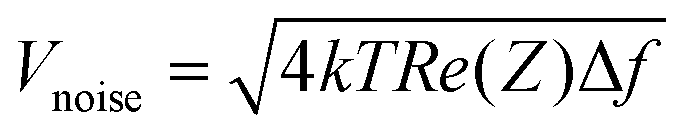
| Fig. 1 (a) Fabrication process steps of graphene electrodes on a Si substrate. First, the oxide is deposited on the front side of a Si wafer followed by Mo deposition and patterning. Then, graphene is grown on a Mo catalyst. Next, Al/Ti is deposited and patterned on the contact pads. Finally, PR is spin-coated and patterned as an insulation layer and Mo is removed from the electrode sites, leaving graphene contacts (as shown in the cross-sectional view of the graphene electrode). (b) Optical image of the final device with four electrodes. (c) The final device attached and wire-bonded to a PCB. | ||
At the end of the fabrication process, the Si wafer is diced and an epoxy die adhesive is used to attach one device to a printed circuit board (PCB) for further testing (Fig. 1(c)). Next, the Al contact pads are Au wire-bonded to the PCB pads. The contact pad and the attached wire are both covered with a drop of Polydimethylsiloxane (PDMS) for mechanical protection. At this stage, some preliminary measurements are performed to characterize the graphene electrodes (pre-NP measurements). Next, the electrodes are ready for NP printing and post-NP measurements.
 | ||
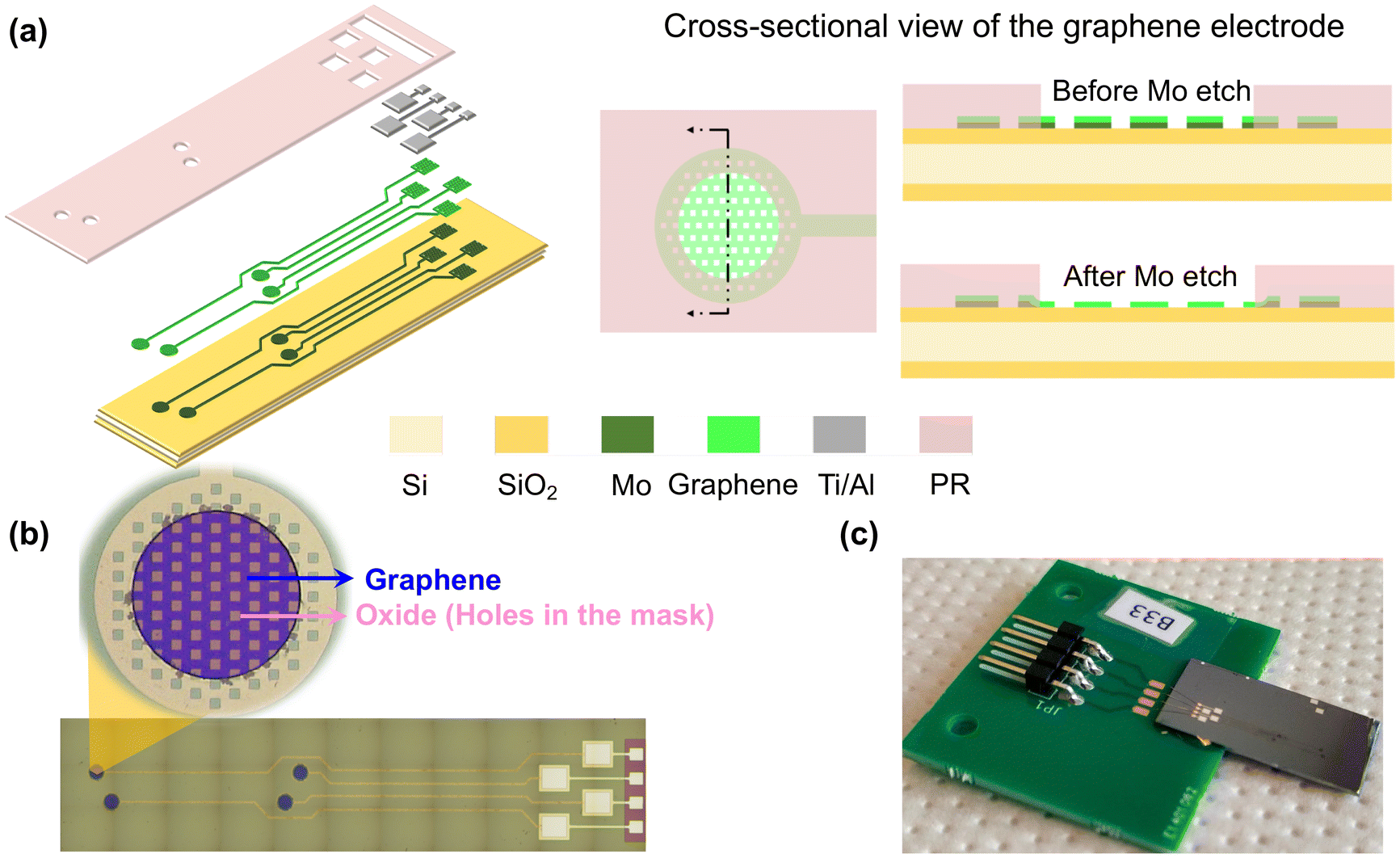
| Fig. 2 Schematic view of the spark ablation method system (VSPARTICLE BV, the Netherlands) used for NP printing. | ||
The substrate is mounted on the stage in the vacuum chamber perpendicular to a 3D-printed converging nozzle with a 0.35 mm diameter as shown in Fig. 2. This nozzle is connected to motors that can navigate in the x, y, and z directions, creating a local printing process. The nozzle aerodynamically focuses the NPs and deposits them on the substrate by impaction.32 In this work, Pt (99.9% purity) rod electrodes with diameters of 3 mm are used to create Pt NP coating on graphene electrodes.
First, NP printing is performed on silicon dies from a nozzle height of 0.5 mm in single-line patterns by varying printing speeds. Then, the Si dies are inspected by scanning electron microscopy (SEM), and the corresponding images are analyzed to calculate the obtained NP densities per each printing speed. Finally, the printing speed to achieve the required NP density is chosen.
For each printer setting, the resulting NP density is determined by averaging the surface density of three SEM images from the same deposition batch. These images are taken with a 2 kV electron beam and 50000× magnification (using a Hitachi Regulus 8230). First, the grey-scale SEM images are converted to black and white (binary) images using MATLAB R2019b (of MathWorks). The pixels whose value is above a certain threshold are replaced with white, representing the area covered with NPs, and the pixels with values below the threshold are considered black. Otsu's method33 is used to determine the optimal threshold to convert the grey-scale images into binary images. The percentage of white pixels out of all pixels is considered the density of the NPs.
To ensure that the width of the printed NP line is sufficient to cover the electrode surface, it is necessary to measure the line width. SEM images taken at low magnification (×50) at a 2 kV accelerating voltage are used for this purpose. The grey-scale images are converted to binary images through Otsu's thresholding method. The data matrix includes columns of 0 s and 1 s and the longest series of 1 s across a column is considered the width. The average length of that data matrix is then used as the width of the printed line. This value is subsequently converted to millimeters using ImageJ (an image analysis program developed at the National Institute of Health34).
It should be noted that the printed line should not conduct electricity to prevent enlarging the circular electrode surface area into an extended line. To ensure low conductivity of the printed NP lines, a conductivity measurement is performed using a four-point probe (Cascade Microtech probe station) on gold Van der Pauw structures covered with an NP line with the same density printed over them.
2.2. Electrode characterization
2.3. Stability assessments
Printing NPs on the graphene electrode surfaces is performed to reduce the electrode impedance and increase the CSC. This electrochemical improvement should remain stable for the lifetime of the device. Coating stability includes both electrochemical and mechanical stability, meaning the electrode should maintain its electrochemical improvement and the coating should not delaminate from the electrode surface. Therefore, the electrochemical and mechanical stability of the NPs must be verified prior to any electrode implantation in the body.To this aim, continuous CV and VT tests are performed to ensure the electrochemical stability of the electrodes. Finally, an ultrasonic vibration test is performed to evaluate the mechanical stability of the NP coating.
000 as the Mo layer underneath the graphene tracks started to corrode. The test is conducted for two electrodes: one graphene electrode without any NP coating and one graphene electrode with 40% NP coating. The characterization of the electrodes is performed before and after the continuous VT test by performing Raman spectroscopy, EIS, and CV measurements.
3. Results
3.1. NP printing
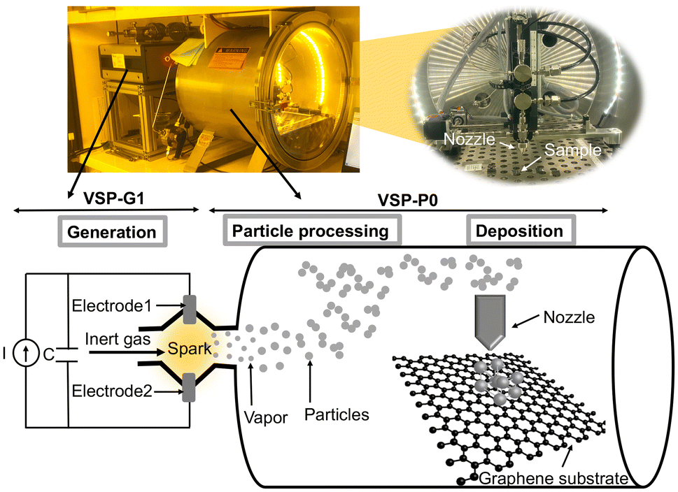
Fig. 3(a) shows the SEM images of NPs printed on Si dies with the required surface densities. The corresponding binary image of 40% Pt NPs is also depicted. The settings and parameters used for Pt NP printing are shown in Table S1 in the ESI.† The resulting printed line width, calculated from the binary images for the various NP densities, is also reported in this table. In all cases, the lines are wide enough to ensure that NPs are printed on the entire electrode surface with a diameter of 340 μm. | ||
| Fig. 3 (a) The original grey-scale SEM images after calculating the surface density of NPs, with the corresponding binary image of 40% NP density, (b) the optical image of graphene electrode before and after 15% NP printing, (c) Raman spectroscopy measurement of graphene without and with 40% Pt NPs, (d) optical transmittance of multiple densities of Pt NPs (15, 30, and 40%) on glass slide are shown after removing the effect of the glass (the optical transmittance of 40% Pt NP is interpolated from 30% and 50% NP densities). Optical transmittance of graphene without Pt NP coating (after removing glass contribution) is added as a reference. | ||
Furthermore, the results of the conductivity measurement can be found in Fig. S1 in the ESI.† The measurement on the printed Pt NP lines over gold Van der Pauw structures shows a significant current flow for NP surface densities of 50%. Therefore, the NP surface density is kept below 40% for this study to prevent any potential extension of the graphene electrode surface to the printed line, as this would influence the electrochemical tests. Conductivity measurements for these lower densities, discussed in the ESI,† indicated this has not been the case.
Fig. 3(b) shows the optical images of a graphene electrode before and after 15% Pt NP printing. NPs can be seen in the zoomed-in image and an obvious color change in the electrode surface is observed as a result of the presence of NPs.
The Raman spectrum of the graphene with and without Pt NPs is displayed in Fig. 3(c). The spectrum of graphene with 40% Pt NPs is shown in green and the spectrum before printing NPs on graphene is displayed in black as a reference. Three distinct peaks can be observed for both spectra: a D peak at 1354 cm−1, a G peak at 1582 cm−1 related to the sp2 C–C bonds forming the graphene lattice, and a 2D peak around 2709 cm−1. No differences are observed in the average intensity ratio of the D to G peaks (I(D)/I(G)) after NP printing (0.19 for graphene and 0.17 for graphene with Pt NPs), implying that Pt NPs did not affect the defect density of graphene. A possible explanation is that nanoparticles are small and sparsely distributed over the surface and they do not have sufficient kinetic energy to cause defects. The mechanism of printing NPs probably results in physically adsorbed clusters causing NPs to have minimal interaction with the graphene lattice.
The optical transmission of multiple surface densities of Pt NP on a glass slide (after removing the effect of the glass slide) versus the wavelength is shown in Fig. 3(d). The optical transmittance measurement was not directly performed for 40% NP surface density. The result shown in the graph is the interpolation of the optical transmittance of 30% and 50% (not shown) NP densities. As shown in the graph, the optical transmittance of the NPs with 40% surface density is still above 92% over a wide range of wavelengths.
The surface roughness measurement on the printed Pt NPs on Si dies is performed for five samples per surface density. The average and standard deviation of RMS and mean surface roughness for each NP surface density are reported in Table S2 in the ESI.† The reported values show a higher average for both RMS and mean roughness by increasing the NP surface density from 15 to 40% (from 9 to 14.67 nm for RMS and from 7.1 to 12 nm for mean surface roughness). An increase in the standard deviation of both RMS and mean surface roughness by increasing the NP density confirms the non-uniformity of printed NPs over the surface. It should be noted that the surface roughness of multilayer graphene electrodes with the same growth condition was reported to be 6.75 nm (ref. 11) which is smaller than the surface roughness of printed Pt NPs.
More information on the measurement methods for Raman spectroscopy, optical transmittance, and surface roughness measurements can be found in the ESI.†
3.2. Electrode characterization
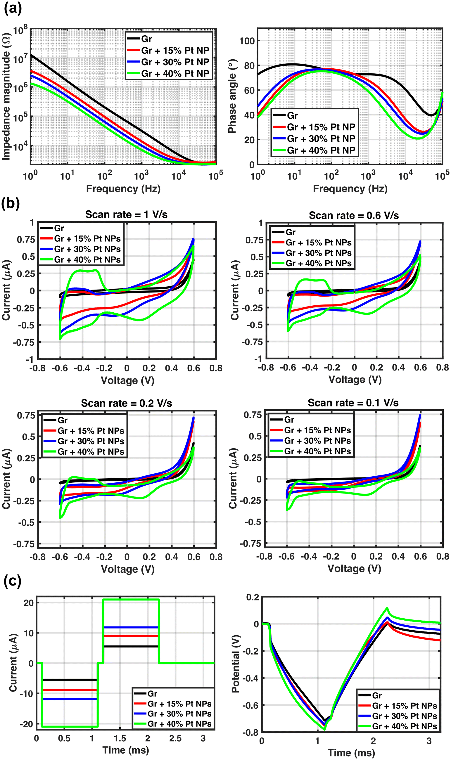 | ||
| Fig. 4 (a) Average EIS results of 7 samples per graphene without Pt NPs and 5 samples per each set of NP surface densities, (b) CV curves of the median sample of each category of graphene without and with NPs with different surface densities, (c) the median of the maximum-amplitude current pulse applied to 5 electrodes per each category of different NP densities with the corresponding VT measurement. | ||
| Measurement results | Graphene | Graphene + 15% Pt NPs | Graphene + 30% Pt NPs | Graphene + 40% Pt NPs | ||
|---|---|---|---|---|---|---|
| Impedance at 1 kHz (kΩ) | 31.45 ± 5.88 | 14.29 ± 0.95 | 9.32 ± 0.80 | 7.26 ± 0.90 | ||
| Area-normalized impedance (Ω cm2) | 21.49 ± 4 | 9.8 ± 0.6 | 6.4 ± 0.5 | 4.96 ± 0.6 | ||
| CSC (μC cm−2) | Total | 1 V s−1 | 248 ± 185 | 551 ± 73 | 745 ± 91 | 954 ± 103 |
| 0.6 V s−1 | 349 ± 272 | 778 ± 109 | 959 ± 159 | 1199 ± 99 | ||
| 0.2 V s−1 | 817 ± 666 | 1887 ± 268 | 1960 ± 504 | 2444 ± 368 | ||
| 0.1 V s−1 | 1566 ± 1277 | 3497 ± 495 | 3399 ± 1062 | 4365 ± 821 | ||
| Cathodic | 1 V s−1 | 78 ± 52 | 345 ± 84 | 469 ± 73 | 651 ± 45 | |
| 0.6 V s−1 | 95 ± 63 | 496 ± 146 | 625 ± 118 | 878 ± 88 | ||
| 0.2 V s−1 | 159 ± 102 | 1211 ± 439 | 1327 ± 367 | 1993 ± 429 | ||
| 0.1 V s−1 | 233 ± 146 | 2197 ± 849 | 2207 ± 746 | 3614 ± 892 | ||
| Max. current amplitude (μA) | 5.7 ± 1.5 | 8.6 ± 1.3 | 12.5 ± 1.5 | 20.9 ± 1.2 | ||
| CIC (μC cm−2) | 8.4 ± 2.1 | 12.6 ± 1.9 | 18.3 ± 2.2 | 30.6 ± 1.8 | ||
3.3. Stability assessment
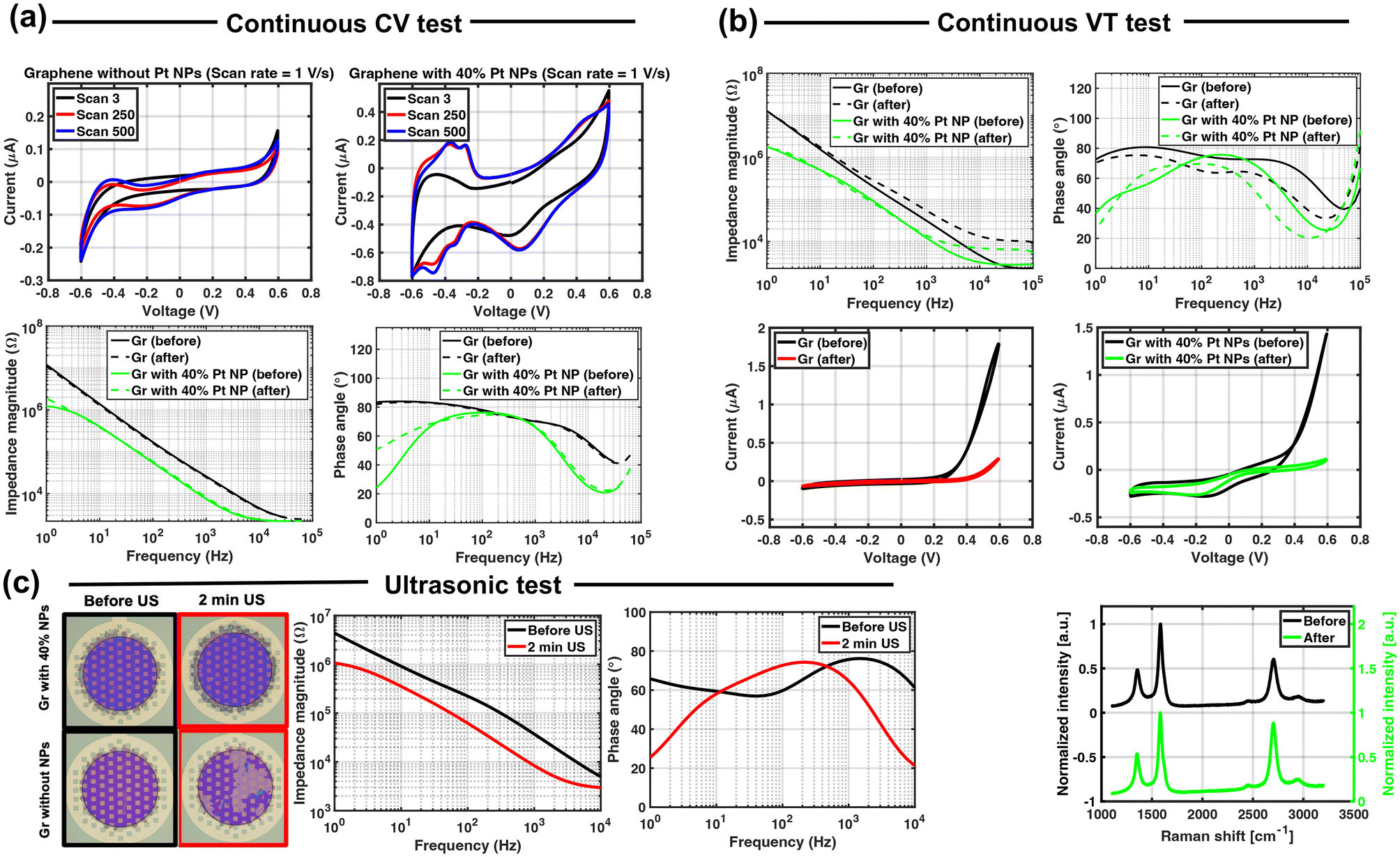 | ||
| Fig. 5 Stability assessment results. (a) Continuous-CV test results: CV curves of graphene without NP and graphene with 40% NP after 3, 250, and 500 cycles, and impedance magnitude and phase plot of graphene without NP and with 40% NP before and after 500 cycles of CV, (b) continuous VT test results: impedance magnitude and phase plot of graphene electrodes without and with 40% NP coatings before and after 500000 cycles of VT test, CV curves of graphene electrodes without and with 40% Pt NP coatings before and after continuous VT test, and Raman spectra of a graphene electrode with 40% NP coatings before and after continuous VT test, (c) ultrasonic test results: an optical image of graphene electrodes with and without NPs before and after 2 minutes of ultrasonication, and impedance magnitude and phase plot of graphene electrode with 40% NP density before and after 2 minutes of ultrasonication. | ||
A CV enlargement is observed for 7 out of 9 graphene electrodes with Pt NP coating after 500 cycles of CV (shown in Table S3 in the ESI†). A shoulder at 0.25 V is observed that corresponds to oxide formation, and a peak at 0.10 V is attributed to the oxide reduction. Peaks for hydrogen adsorption and desorption were also observed around −0.40 V as reported previously.36 Comparing the CV curves after 250 and 500 cycles shows that the CV curve seems to be stabilized and no significant change is observed after 250 cycles. Although the CV enlargement is observed for graphene electrodes with various Pt NP densities after 500 CV cycles, the electrodes with 40% NPs show the largest increase in CSC of around 16.9%. This can be related to more oxidation and reduction as a result of more Pt NPs and, therefore, higher peaks in CV. The CV curve reduction of 2 out of 9 electrodes is inconclusive and cannot be attributed to the delamination of Pt NPs. To draw any conclusions, more samples should be tested and the number of CV cycles should be also increased.
The impedance of 7 out of 9 graphene electrodes with Pt NPs shows an average of 15% increase. This increase could be attributed to Pt NP delamination which could increase the impedance. However, if there is any delamination of NPs the CSC is expected to decrease. It might be argued that the appearance of the peaks related to oxidation and reduction compensates for the NP delamination. However, if this were the case, the delamination is expected to continue even after 250 CV cycles.
Finally, the EDX measurement on the electrode surface after a continuous CV test (shown in Fig. S2 in the ESI†) confirms the presence of the coating by showing Pt peaks corresponding to Pt NPs.
CV curves for graphene electrodes without and with 40% NP coating are shown in Fig. 5(b). In both cases a reduction in the CV area is observed after 500000 cycles of the VT test, indicating some electrochemical change in the graphene electrode. However, the CSC for the NP-coated electrodes remains higher than the one of graphene only, further suggesting the presence of NP still after the continuous-VT test.
The Raman spectra acquired on the graphene electrode with 40% NP coating before and after this test show three graphene characteristics, confirming the presence of graphene after the continuous-VT test as shown in Fig. 5(b). However, the I(D)/I(G) ratio slightly increased from 0.2 to 0.35 probably due to the defects induced into the graphene lattice. This ratio did not change for the graphene electrode without any coatings.
4. Discussion
The multilayer graphene electrode surface is modified with Pt NPs to enhance its electrochemical characteristics. A spark ablation method is used to print NPs locally on the electrodes. This single-step process can be performed at room temperature in a dry environment. The surface modification practically enables the use of smaller electrodes with higher selectivity for neural recordings and allows the transfer of more charge via the electrode–tissue interface for neural stimulation under electrochemically safe conditions. Furthermore, the NP deposition at room temperature enables a stress-free NP coating deposition, which does not involve thermally introduced strain forces to the electrode.18The highest NP surface density used in this work is 40% which still has an optical absorbance below 8%. The optical transmittance of graphene with the same growth condition was previously reported to be above 80%.11 This confirms the potential use of graphene electrodes coated with NPs for future neuroscientific research such as optogenetics and optical imaging, as adding NPs on the graphene electrode surface is not expected to have a significant impact on the electrode's optical transparency.
The results reported in this work demonstrate an improvement of the electrochemical characteristics of graphene electrodes by adding printed Pt NP coatings. The electrochemical performance is further improved for higher NP surface densities. This improvement is likely a result of the electrode surface area increase due to the presence of NPs and the fact that Pt NPs create a parallel conduction path in the electrode–electrolyte interface, overcoming the quantum capacitance of graphene.19 CSC values are also known to be influenced by factors such as surface roughness, electrochemical surface area, and charge transfer mechanisms of the coating.36 Previously reported monolayer graphene electrodes with electrodeposited Pt NP coatings have a similar area-normalized impedance for 15% NP density.19 Concerning CSC and CIC for neural stimulation applications, no comparison can be made with the previous work which focuses only on neural recording measurements. The results from CV and VT measurements demonstrate 15 times higher CSC, and 4 times better CIC after Pt NP printing on the graphene surface. Unfortunately, in the aforementioned work, the stability of the coating on graphene was also not investigated. In this work, three different tests were used to assess the coating stability, electrochemically and mechanically.
Continuous CV tests show that the electrodes with printed Pt NPs are electrochemically stable. Examination of the electrode surface after continuous CV measurements did not reveal any delamination or cracks on the graphene samples with NP coating. To further investigate the electrochemical stability of the electrodes, a larger number of CV cycles could be used.
Continuous VT tests do not suggest substantial delamination of the Pt NP coating from the graphene electrode surface. Similar impedance and CSC changes are observed for the graphene electrode without any coating which could be attributed to graphene delamination from the oxide layer. The reported impedance of the electrode with coating after 500000 VT cycles is still lower than the impedance of graphene electrodes without any coating. This test should be repeated for the final implantable device as this device will not have a Mo layer underneath graphene which restricted this test due to Mo corrosion. The presence of the Mo layer probably had a negative impact on the results.
Ultrasonic treatment has been applied to the coated electrodes to assess the mechanical stability of the coating. Results from this test do not suggest NP delamination after the treatment, as indicated by optical inspection and impedance measurements. Surprisingly, graphene electrodes coated with NPs remain adherent to the underlying oxide layer, while graphene electrodes alone delaminate from it during the treatment. Ultrasonication has been used in literature to test the mechanical stability and adhesion of other coatings, such as PEDOT:PSS, on various electrode materials.39 However, the ultrasonic vibration applied by this test to the electrodes is quite intense and harsh, and not representative of what an electrode will encounter in the body environment.
Nevertheless, the electrochemical and mechanical stability of the Pt NP coating of graphene electrodes suggest that printed NPs are quite stable. It is not clear whether the stability of printed NPs is because of the printing method, the multilayer nature of our graphene, or some other factor. It would certainly be interesting to compare the stability of the NP deposited with other deposition techniques and/or single-layer graphene, but unfortunately, these results are lacking in the literature.
The test samples used for the stability assessment of the Pt NP coating on graphene in this work have not been optimised for these tests. In particular, the samples have been fabricated on a Si substrate where graphene sits on a silicon oxide layer, from which it delaminates during the continuous VT and ultrasonic treatments. This fact limited the intensity or duration of the treatment. In a practical application scenario of a neural interface, the oxide layer underneath the graphene electrodes is removed and substituted with parylene, as shown in ref. 11. Therefore, to ensure a more conclusive result the stability tests should be repeated and extended for the final device. The delamination of the NP coating leads to the deterioration of the electrochemical characteristics over time, which consequently results in functionality loss. Moreover, the detached NPs may undergo biodispersion inside the body after implantation and can become toxic to the tissue. Additional treatments, such as prolonged immersion in a PBS solution, or dipping in an agarose gel,38 could be added to the current suite, to further assess the long-term adhesion and stability of the coating for potential chronic applications.
If necessary, roughening the electrode surface prior to NP printing could be investigated in the future as a means to enhance the NP adhesion to the electrode surface. Previously, roughening the electrode surface of metal electrodes prior to PEDOT:PSS coating resulted in an increase in mechanical bonding between the electrode and its coating, thereby resulting in higher stability.39
The NP deposition technique presented in this paper yields a selective local modification of graphene electrodes. This opens up interesting possibilities when arrays of electrodes of various sizes are required during multimodal interaction with neural tissue. NP coatings come at the expense of less transparency, therefore could only be applied locally, only at e.g., very small electrodes, to enhance their recording performance, while larger electrodes on the same device can remain uncoated. Besides their effect on electrochemical characteristics, Pt NPs can be employed for local biosensing. This localization is not possible with electrodeposition techniques, where all electrodes on a device will be coated simultaneously. Besides, but crucially, the proposed technique is performed at room temperature and via a dry process, as a post-processing step. It is thus compatible with polymer substrates, an integral component of neural implants, as well as with a range of other processes and materials of the final device. These characteristics render this approach a unique tool for the enhancement of the performance of flexible neural implants.
Finally, the Pt NP coating on graphene electrodes used in this paper shows that significant improvement in the electrochemical characteristics of multilayer graphene while maintaining a large degree of transparency is possible per electrode. It demonstrates a reduction in the impedance and a significant increase in CSC and CIC, quantities that are essential for efficient neural tissue interaction. The stability of the Pt NPs on the graphene surface was also assessed, for the first time, in scenarios relevant and tailored to their use during neural interfacing.
5. Conclusions
To conclude, we present multilayer graphene electrode surface modification with Pt NPs using a spark ablation method. This method yields the local printing of NPs on an electrode surface without using a high temperature or wet processing. NP printing can be performed as a post-processing step to enhance the electrochemical characteristics of graphene electrodes further. The electrode showed 4.5 times lower impedance at 1 kHz after 40% NP coating on the surface (from 31.45 to 7.26 kΩ). The charge storage capacity (CSC), calculated based on a cyclic voltammetry (CV) test, was improved up to 15 times with 40% NP coating (from 233 μC cm−2 to 3614 μC cm−2). The maximum charge injection capacity (CIC), obtained by voltage transient (VT) measurements, also increased from 8.4 μC cm−2 for graphene electrodes to 30.6 μC cm−2 for graphene-coated electrodes with 40% surface density of NPs. NPs printed using this method yield electrochemical stability over 500 cycles of continuous CV measurements and 500000 cycles of continuous VT tests. In addition, ultrasonic vibration of electrodes with NP coating shows better mechanical stability compared to graphene electrodes without any NPs. These results demonstrate selective NP deposition and local modification of electrochemical properties in graphene electrodes for the first time, enabling the cohabitation of graphene electrodes with different electrochemical and optical characteristics on the same substrate for neural interfacing.
Conflicts of interest
There are no conflicts to declare.Acknowledgements
This research was supported by the POSITION-II project funded by the ECSEL JU under grant number Ecsel-783132-Position-II-2017-IA. The authors would like to thank the staff members of the Else Kooi Laboratory (EKL) for their support in the lab and VSPARTICLE B.V. for the use of their equipment.References
- C. Grienberger and A. Konnerth, Neuron, 2012, 73, 862–885 CrossRef CAS PubMed.
- M. Scanziani and M. Häusser, Nature, 2009, 461, 930–939 CrossRef CAS PubMed.
- J. A. Frank, M.-J. Antonini and P. Anikeeva, Nat. Biotechnol., 2019, 37, 1013–1023 CrossRef CAS PubMed.
- A. Canales, X. Jia, U. P. Froriep, R. A. Koppes, C. M. Tringides, J. Selvidge, C. Lu, C. Hou, L. Wei and Y. Fink, et al. , Nat. Biotechnol., 2015, 33, 277–284 CrossRef CAS PubMed.
- F. Wu, E. Stark, M. Im, I.-J. Cho, E.-S. Yoon, G. Buzsáki, K. D. Wise and E. Yoon, J. Neural Eng., 2013, 10, 056012 CrossRef PubMed.
- T. D. Kozai and A. L. Vazquez, J. Mater. Chem. B, 2015, 3, 4965–4978 RSC.
- S. Guan, J. Wang and Y. Fang, Nano Today, 2019, 26, 13–15 CrossRef.
- M. Thunemann, Y. Lu, X. Liu, K. Kılıç, M. Desjardins, M. Vandenberghe, S. Sadegh, P. A. Saisan, Q. Cheng and K. L. Weldy, et al. , Nat. Commun., 2018, 9, 1–12 CrossRef CAS PubMed.
- D. Kireev and A. Offenhäusser, 2D Mater., 2018, 5, 042004 CrossRef CAS.
- C. Zhan, J. Neal, J. Wu and D.-E. Jiang, J. Phys. Chem. C, 2015, 119, 22297–22303 CrossRef CAS.
- N. Bakhshaee Babaroud, M. Palmar, A. I. Velea, C. Coletti, S. Weingärtner, F. Vos, W. A. Serdijn, S. Vollebregt and V. Giagka, Microsyst. Nanoeng., 2022, 8, 1–14 CrossRef PubMed.
- A. I. Velea, S. Vollebregt, G. K. Wardhana and V. Giagka, 2020 IEEE 33rd International Conference on Micro Electro Mechanical Systems (MEMS), 2020, pp. 421–424.
- D.-W. Park, A. A. Schendel, S. Mikael, S. K. Brodnick, T. J. Richner, J. P. Ness, M. R. Hayat, F. Atry, S. T. Frye and R. Pashaie, et al. , Nat. Commun., 2014, 5, 1–11 Search PubMed.
- N. A. Kotov, J. O. Winter, I. P. Clements, E. Jan, B. P. Timko, S. Campidelli, S. Pathak, A. Mazzatenta, C. M. Lieber and M. Prato, et al. , Adv. Mater., 2009, 21, 3970–4004 CrossRef CAS.
- V. Giagka and W. A. Serdijn, Bioelectron. Med., 2018, 4, 1–10 CrossRef PubMed.
- J. B. Johnson, Phys. Rev., 1928, 32, 97 CrossRef CAS.
- H. Nyquist, Phys. Rev., 1928, 32, 110 CrossRef CAS.
- C. Boehler, T. Stieglitz and M. Asplund, Biomaterials, 2015, 67, 346–353 CrossRef CAS PubMed.
- Y. Lu, X. Liu, R. Hattori, C. Ren, X. Zhang, T. Komiyama and D. Kuzum, Adv. Funct. Mater., 2018, 28, 1800002 CrossRef PubMed.
- Y.-S. Kim, K. Kumar, F. T. Fisher and E.-H. Yang, Nanotechnology, 2011, 23, 015301 CrossRef PubMed.
- G. H. Kim, N. Y. Kim, Z. Lee, S. D. Jung and J.-O. Lee, et al. , RSC Adv., 2017, 7, 3273–3281 RSC.
- P. Kshirsagar, S. Dickreuter, M. Mierzejewski, C. J. Burkhardt, T. Chassé, M. Fleischer and P. D. Jones, Adv. Mater. Technol., 2019, 4, 1800318 CrossRef.
- F. Sun, Z. Xiong, J. Park and G. Xu, IEEE Trans. Electron Devices, 2021, 68, 3080–3086 CAS.
- Z. Zhao, R. Gong, H. Huang and J. Wang, Sensors, 2016, 16, 880 CrossRef PubMed.
- A. T. Young, N. Cornwell and M. A. Daniele, Adv. Funct. Mater., 2018, 28, 1700239 CrossRef PubMed.
- F. Gunes, H.-J. Shin, C. Biswas, G. H. Han, E. S. Kim, S. J. Chae, J.-Y. Choi and Y. H. Lee, ACS Nano, 2010, 4, 4595–4600 CrossRef CAS PubMed.
- Y.-G. Zhou, J.-J. Chen, F.-B. Wang, Z.-H. Sheng and X.-H. Xia, Chem. Commun., 2010, 46, 5951–5953 RSC.
- Y. Li, W. Gao, L. Ci, C. Wang and P. M. Ajayan, Carbon, 2010, 48, 1124–1130 CrossRef CAS.
- H. Wu, J. Wang, X. Kang, C. Wang, D. Wang, J. Liu, I. A. Aksay and Y. Lin, Talanta, 2009, 80, 403–406 CrossRef CAS PubMed.
- P. Yin, Y. Liu, L. Xiao and C. Zhang, Polymers, 2021, 13, 2834 CrossRef CAS PubMed.
- B. K. Poudel, J. Hwang, J. H. Park and J. H. Byeon, Spark Ablation: Building Blocks for Nanotechnology, CRC Press, 2019, pp. 373–420 Search PubMed.
- T. Pfeiffer, J. Feng and A. Schmidt-Ott, Adv. Powder Technol., 2014, 25, 56–70 CrossRef CAS.
- N. Otsu, IEEE transactions on systems, man, and cybernetics, 1979, 9, 62–66 Search PubMed.
- S. M. Hartig, Curr. Protoc. Mol. Biol., 2013, 102, 14–15 Search PubMed.
- C. Boehler, S. Carli, L. Fadiga, T. Stieglitz and M. Asplund, Nat. Protoc., 2020, 15, 3557–3578 CrossRef CAS PubMed.
- S. F. Cogan, Annu. Rev. Biomed. Eng., 2008, 10, 275–309 CrossRef CAS PubMed.
- G. Schiavone, X. Kang, F. Fallegger, J. Gandar, G. Courtine and S. P. Lacour, Neuron, 2020, 108, 238–258 CrossRef CAS PubMed.
- V. Ramesh, N. Stratmann, V. Schaufler, S. D. Angelov, I. D. Nordhorn, H. E. Heissler, R. Martínez-Hincapié, V. Čolić, C. Rehbock and K. Schwabe, et al. , Adv. Healthcare Mater., 2022, 2102637 CrossRef CAS PubMed.
- A. S. Pranti, A. Schander, A. Bödecker and W. Lang, Sens. Actuators, B, 2018, 275, 382–393 CrossRef CAS.
Footnote |
| † Electronic supplementary information (ESI) available. See DOI: https://doi.org/10.1039/d3nr05523j |
| This journal is © The Royal Society of Chemistry 2024 |