
 Open Access Article
 This Open Access Article is licensed under a
 Creative Commons Attribution 3.0 Unported Licence
Tuning dipolar and multipolar resonances of chiral silicon nanostructures for control of near field superchirality†
Dominic J. P.
Koyroytsaltis-McQuire
*a,
Rahul
Kumar
a,
Tamas
Javorfi
b,
Giuliano
Siligardi
 b,
Nikolaj
Gadegaard
c and
Malcolm
Kadodwala
*a
b,
Nikolaj
Gadegaard
c and
Malcolm
Kadodwala
*a
aSchool of Chemistry, University of Glasgow, Glasgow, G12 8QQ, UK. E-mail: Malcolm.kadodwala@glasgow.ac.uk; d.koyroytsaltis-mcquire.1@research.gla.ac.uk
bDiamond Light Source Ltd, Harwell Science and Innovation Campus, Didcot, UK
cSchool of Engineering, Rankine Building, University of Glasgow, Glasgow G12 8LT, UK
First published on 5th December 2023
Abstract
Chiral materials display a property called optical activity, which is the capability to interact differentially with left and right circularly polarised light. This leads to the ability to manipulate the polarisation state of light, which has a broad range of applications spanning from energy efficient displays to quantum technologies. Both synthesised and engineered chiral nanomaterials are exploited in such devices. The design strategy for optimising the optical activity of a chiral material is typically based on maximising a single parameter, the electric dipole–magnetic dipole response. Here we demonstrate an alternative approach of controlling optical activity by manipulating both the dipole and multipolar response of a nanomaterial. This provides an additional parameter for material design, affording greater flexibility. The exemplar systems used to illustrate the strategy are nanofabricated chiral silicon structures. The multipolar response of the structures, and hence their optical activity, can be controlled simply by varying their height. This phenomenon allows optical activity and the creation of so called superchiral fields, with enhanced asymmetries, to be controlled over a broader wavelength range, than is achievable with just the electric dipole–magnetic dipole response. This work adds to the material design toolbox providing a route to novel nanomaterials for optoelectronics and sensing applications.
Introduction
The amplification of chiral light–matter interactions are key for the development of novel sensing technologies. This is due to the inherent lack of sensitivity in traditional methods such as circular dichroism (CD) used to study chiral (bio)molecules. Nanophotonic platforms are key to delivering these new technologies since they provide a mechanism for significantly enhancing chiral light–matter interactions. One property that is central to sensing applications is the ability to generate electromagnetic fields with chiral asymmetry exceeding that of circularly polarised light (CPL), sometimes referred to as superchiral light. A chiroptical response of a material is usually defined by the electric dipole (ED) and magnetic dipole (MD) cross terms. Optimising the EDMD terms is the usual strategy for maximising the chiroptical response in both nanophotonic1–3 and molecular systems.4,5 Studies which exploit nanophotonics to amplify chiral light matter interactions have predominately focused on plasmonic nanostructures.6 This emphasis on plasmonic platforms is primarily driven by the ease of fabrication. However, a key limitation of plasmonic systems is high ohmic losses, which may be sub-optimal for some sensing and optoelectronic applications. This has led to a greater consideration for all-dielectric nano/metamaterials, which are capable of a wide range of electromagnetic responses and suffer low ohmic losses from the visible to telecommunications range.7–9 In the context of using nanophotonics for amplifying chiral light matter interactions, dielectric materials have another significant advantage. Through controlling the dimensions of dielectric structures, electric and magnetic dipole resonances can be made to spectrally overlap, enhancing the near and far field chiroptical properties. However, this can only be achieved in a relatively narrow wavelength window within the visible region of the spectrum. In the case of anisotropic chiral materials, higher order multipolar terms, which average to zero in isotropic media, can also contribute to the chiroptical response. These multipolar contributions to chiroptical effects can be very significant (at least comparable to the EDMD response) for nano/metamaterials which have near fields with intrinsically large gradient.10 The concept tested in this study is that the near and far field chiroptical properties of a silicon metamaterial can be controlled by manipulating the dipole and multipolar responses through modifying a single form factor parameter, the height, of the constituent nanostructures. We show through a combination of experiment and numerical simulation, that chiroptical behaviour, including the superchirality of the near fields, has a significant contribution from the ED and electric quadrupole EQ cross terms. Birefringence effects, arising from the lack of four-fold rotational symmetries of the metasurfaces, have been decoupled from the true chiroptical responses using Mueller matrix polarimetry.Metasurface design
The metasurfaces used in this study are based on an S structure, Fig. 1a–c, which is chiral due to the presence of the underlying substrate breaking the horizontal mirror symmetry. The S structures possess C1 symmetry due to the asymmetric spacing between the top and bottom arms with respect to the middle arm, with the arms having 20 nm less separation, Fig. 1a. The S structure was used to create four distinct metasurfaces based on square arrays with periodicities of 850 nm. The four arrays, shown in Fig. 1b, include left and right-handed (LH and RH) enantiomorphs and two racemic types (i.e., they contain equal numbers of LH and RH structures and thus for perfect structures would have no net optical activity). One type of racemic array, referred to as RA, contains alternating domains consisting of 19 × 19 sub-arrays of either LH or RH structures. The other racemic form, referred to as RS, contains alternating individual LH and RH structures, of which an AFM image is shown in Fig. 1c. Each metasurface was fabricated to occupy 0.25 mm2 and contains 600 × 600 structures. The metasurfaces where fabricated with structures of four different heights, 160, 180, 210, and 240 nm (see ESI S1†).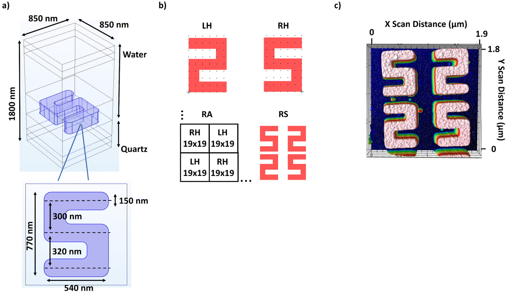 | ||
| Fig. 1 (a) The unit cell containing an idealised RH geometry used to model the structures in numerical simulations, with labelled feature sizes. (b) Designs for the repeating units of each array are illustrated. (c) An AFM image of LH and RH structures as part of the RS array. | ||
Results and discussion
Reflectance spectra
The light scattering behaviour of the metasurfaces were investigated via reflectance measurements, obtained relative to the substrate, for the four array types immersed in PBS buffer solution for each sample height, shown in Fig. 2a–d. Spectra were taken at two orthogonal incident polarisations of linearly polarised light (LPL) which are subsequently referred to and labelled as x- and y-polarisations.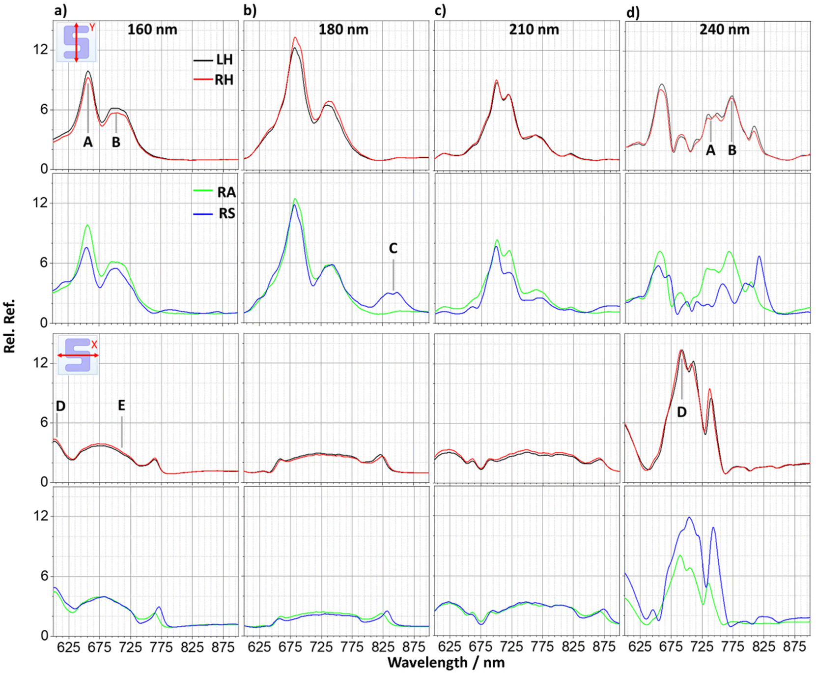 | ||
| Fig. 2 Experimentally measured y- and x-polarised relative reflectance for LH (black), RH (red), RA (green) and RS (blue) arrays for silicon structure heights of (a) 160 nm, (b) 180 nm, (c) 210 nm and (d) 240 nm. Peaks of interest are labelled A–E. | ||
As would be expected, the spectra collected from the enantiomorphic pairs and the RA racemic structure are very similar. For the 160, 180 and 210 nm thick LH, RH and RA samples, Fig. 2a–c, the y-polarised spectra show a double peak, with two dominant components we have labelled A and B. There is a progressive red shift in reflectance features as the silicon height increases. For a thickness of 210 nm the A component undergoes a split. At a thickness of 240 nm there is an abrupt change in spectral profile, Fig. 2d, which is more significant than the progressive change observed between 160 to 210 nm. There is an appearance of a single peak close to 660 nm and a broad feature between 725 nm to 825 nm that contains multiple components.
The x-polarised spectra for LH, RH and RA substrates with heights 160–210 nm display broad and relatively weak reflectance, in contrast to intense resonances in the equivalent y-polarisation data. The general shape of the spectra (a broad peak situated between two individual peaks at 605 nm and 765 nm for the 160 nm sample) progressively red shifts as with the x-polarisation data. Once again, at a height of 240 nm the spectra undergo a significant change in form, with a large increase in reflectance intensity between 650 nm and 775 nm. The red shifting of resonances with increasing nanostructure height is analogous to the previously reported effects of increasing size on silicon nanoparticles.11–13 It is consistent with behaviour expected from Mie theory, where resonances are directly proportional to the diameter of the scatterer.14,15 The magnetic dipole resonance for a spherical particle can be approximated to occur at wavelength  , with d the particle diameter and n the refractive index.16 Multipolar resonances are more complex and are described elsewhere.17
The reflectance response of the RS metasurfaces are qualitatively like that of the other three. There is a very strong similarity between y-polarised RS spectra for 160 to 210 nm thick substrates and those from the other arrays. However, the RS arrays have an additional resonance at ∼850 nm, which correlates to the periodicity of the structure, and has subsequently been labelled C. There is a significantly greater difference in spectral line shape for the 240 nm thick substrate in the 650 to 850 nm range. The x-polarisation RS data has smaller differences in overall spectral line shape with those of the other arrays.
Numerical simulation of reflectance data
Numerical electromagnetic modelling has been used to provide insight into the light scattering properties of the silicon metasurfaces. Simulated reflectance spectra, relative to the substate, derived from modelling are shown in Fig. 3a–d. As expected, data for LH and RH enantiomorphs are identical (see ESI S2†), so only the latter are shown. We have assumed that simulated data for the RA racemic structure will be the average of that obtained from the two separate enantiomorphic structures.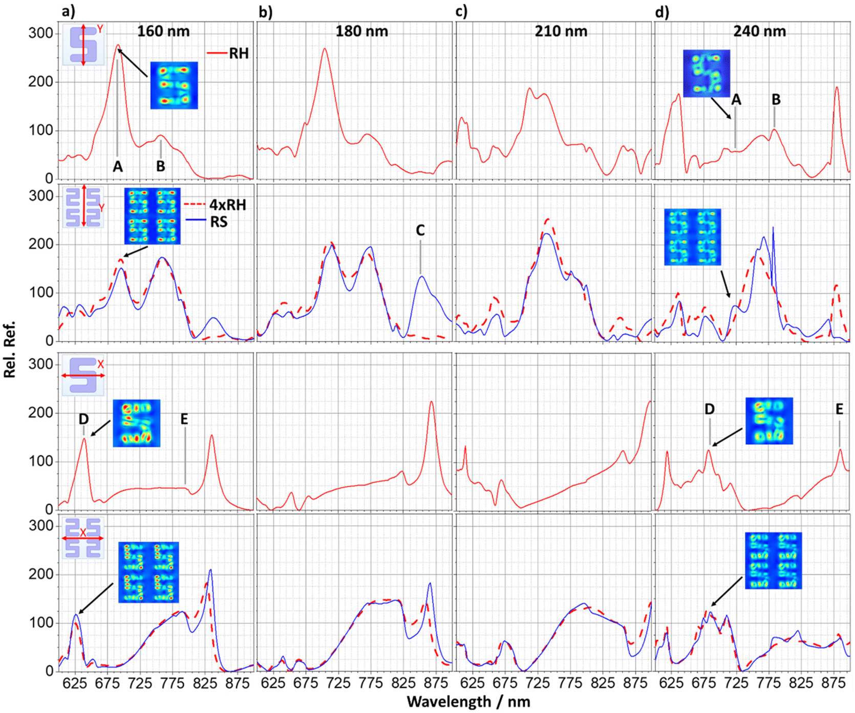 | ||
| Fig. 3 Simulated y- and x-polarised reflectance for each of the 160–240 nm sample heights, (a)–(d). Modelling was performed with a single RH structure (red), four-structured RH models (red dashed) and four-structured RS (blue) arrays. Equivalent peaks with respect to experimental data are labelled A–E. Magnetic field (|H|) distribution maps are labelled for equivalent peaks of the two height extremes. | ||
The simulated reflectance data for both x- and y-polarisation are in reasonable agreement with experimental measurements, both qualitatively replicating line shape and the abrupt change that occurs between 210 and 240 nm. However, the spectra display resonances which are significantly more intense, by a factor of ∼20, than are observed experimentally. This in part can be attributed to structural and compositional heterogeneity (missing structures and chemical contamination which can lead to doping of the silicon and hence larger carrier densities) which are not accounted for in the model. A similar level of discrepancy between simulation and experiment has been observed previously in plasmonic nanoarrays.18
The y-polarised modelling for the enantiomorphic pairs and RS array replicates the double peaks, A and B, for the 160 nm and 180 nm structures, as well as the peak splitting that occurs for peak A at 210 nm thickness. The 240 nm sample reproduces the single peak below 700 nm and the broader range of peaks across the 700–800 nm range.
The x-polarised simulation for the enantiomorphic pairs and RS displays poorer agreement with experiment but do replicate the presence of two peaks either side of a broader region of intensity for the 160–210 nm samples. The simulations do however overestimate the intensity of the sharper peaks. There is further agreement for the 240 nm sample, in which a larger reflectance feature centred at ∼700 nm is observed, although it is less intense compared to experiment. There is also a sloping effect that occurs as the sample height increases from 180–210 nm, where the reflectance intensity is greater at longer wavelengths.
To simulate the RS arrays requires using a model which has a unit cell of four S structures (see ESI S3†), rather than a single structure used for enantiomorphic pair arrays. The larger model reduces the density of elements which degrades the accuracy of the simulations. In Fig. 3, our simulated spectra for RS are compared with RH spectra also derived from a four S containing unit cell. Although the four S models replicate the peaks observed for the single structure model, they have different relative intensities and a loss of feature resolution consistent with the expected decreased accuracy of the simulation. However, the spectra derived from the simulations using four structures for RH and RS are very similar, with the RS showing the additional feature (peak C) observed experimentally. Further analysis of the four S simulations reveal that the characteristic field distributions and intensities are in close agreement with those produced by using simulations based on single structures (see ESI S4†).
A common feature of the simulated data is the red shifting of spectra with respect to experiment. This is attributed to the lack of morphological defects (e.g. surface deformities and wall sloping that stems from limitations in the fabrication process) in the idealised “perfect” structures used for the simulations, which has been observed previously.19 This hypothesis is validated using structural models derived directly from AFM measurements, (see ESI S5†). The use of a ‘real’ AFM model geometry produced spectra in better agreement with experiment. In particular, the AFM model produces spectra with resonances blue shifted relative to those generated with idealised models. The reduced agreement observed between experiment and simulation for the tallest structure is attributed to taller structures being more susceptible to the inaccuracies of the “perfect” idealised model, such as the sloping and lower resolution observed. Due to increased computational resource/time demands associated with the large increase in meshing requirements for AFM models, idealised structures have been used in this work.
Numerical simulation field plots
In addition to the simulated spectra, plots showing the spatial distribution of electric (|E|) and magnetic (|H|) fields have also been generated. The veracity of using data derived from idealised rather than real models is supported by the similarity of the field distributions produced by each for equivalent resonances (see ESI S5†). Only RH fields are shown as LH are mirror image equivalents (see ESI S6†) The field plots for resonances A, B, D and E for the four silicon heights for RH (RA) structure are shown in Fig. 4. For each resonance, similar field distributions are observed for the four heights, albeit with varying intensities. This validates the assignment of the features in the spectra to common resonances which red shift with increasing silicon thickness. The spatial distributions of |E| and |H| fields have a common characteristic. Specifically, regions with the most intense |E| correspond to areas where |H| is weakest, and vice versa. This behaviour is consistent with that of other silicon nanomaterials, in which the electric field pattern represents circulating electric currents (see ESI S7†).20 For all resonances, |H| intensities are strongly localised inside the silicon nanostructure. Also, resonance A has the largest |E| outside the silicon, specifically between the arms of the S nanostructure.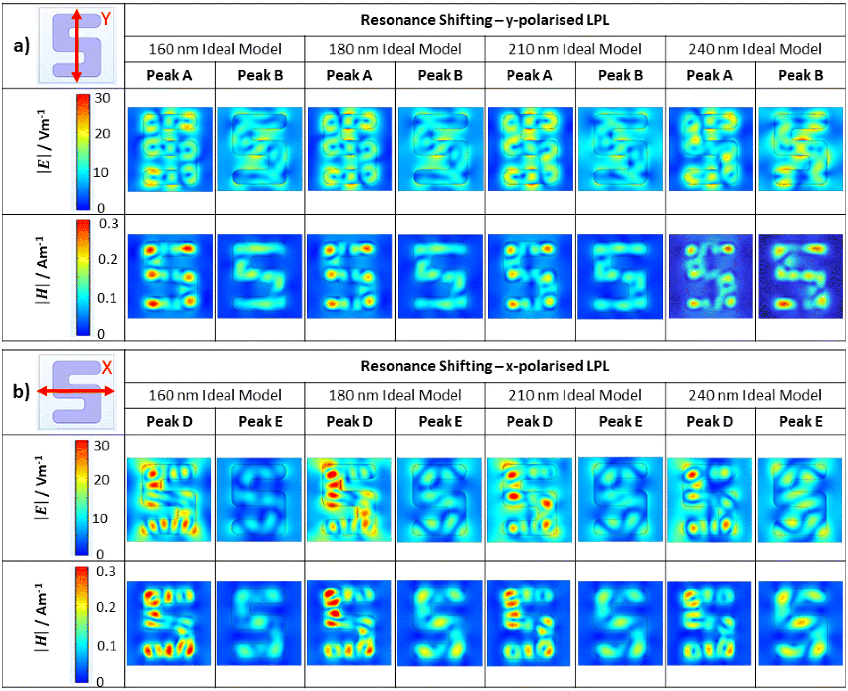 | ||
| Fig. 4 (a) |E| and |H| distributions for peaks A and B. (b) Equivalent data for peaks D and E. Maps shown throughout are taken from the midpoint of the structures. | ||
Field distributions for resonance C, derived from models consisting of four-structured RH and RS arrays, are shown in Fig. 5. The |E| field distributions for the RS array show strong coupling resonances that occur between y-axis-adjacent structures. This indicates that resonance C is associated with coupling between structures, which we term a periodic resonance. This is not observed in the enantiomorphic case, which can be attributed to a less preferential “anti-parallel” alignment of the arms of adjacent structures, limiting their ability to couple. The absence of periodic resonances in the thicker samples can be rationalised by considering a previous study performed on silicon nanoparticle arrays. It was found that the increasing height of the constituent elements also produces a red shift in their periodic resonance.21 In the case of our samples, the periodic resonance therefore shifts out of the detectable range. The simulated periodic resonances are more intense than those observed experimentally, likely due to structural imperfections. As such, the periodic resonance that occurs for the 160 nm simulation at ∼835 nm (which is inherently less intense than the 180 nm sample) is not observed experimentally.
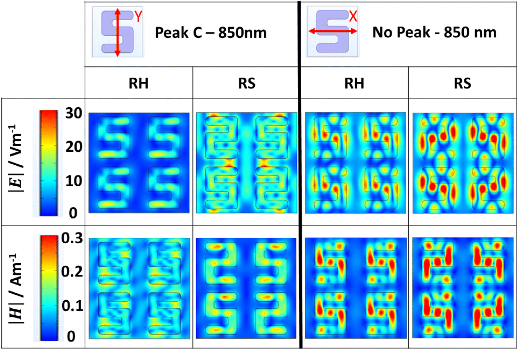 | ||
| Fig. 5 |E| and |H| distributions at the peak C wavelength for 180 nm four-structured RH and RS arrays under y- and x-polarised excitation. | ||
Multipolar analysis
To provide greater insight into the microscopic origins of the resonances observed in light scattering, a multipolar analysis has been performed. Such an analysis provides a framework for the Mie description of light scattering from homogeneous spherical nanoparticles.14 Mie theory expands the scattering of incident light as a series of multipolar contributions. Multipole moments are mathematical functions used to represent the distribution of electromagnetic charge and current within a material. The total scattering field of a structure is therefore a superposition of the fields generated by multipole moments such as the electric dipole (ED), magnetic dipole (MD), electric quadrupole (EQ) and magnetic quadrupole (MQ), considered here.22 It is therefore possible to extract each of their contributions numerically through multipole decomposition, a technique which has been performed on a variety of different structures.23–26 For illustrative purposes, we have performed such analyses on enantiomorphic pairs for silicon heights of 180 and 240 nm, for both y- (Fig. 6) and x- (Fig. 7) light polarisations.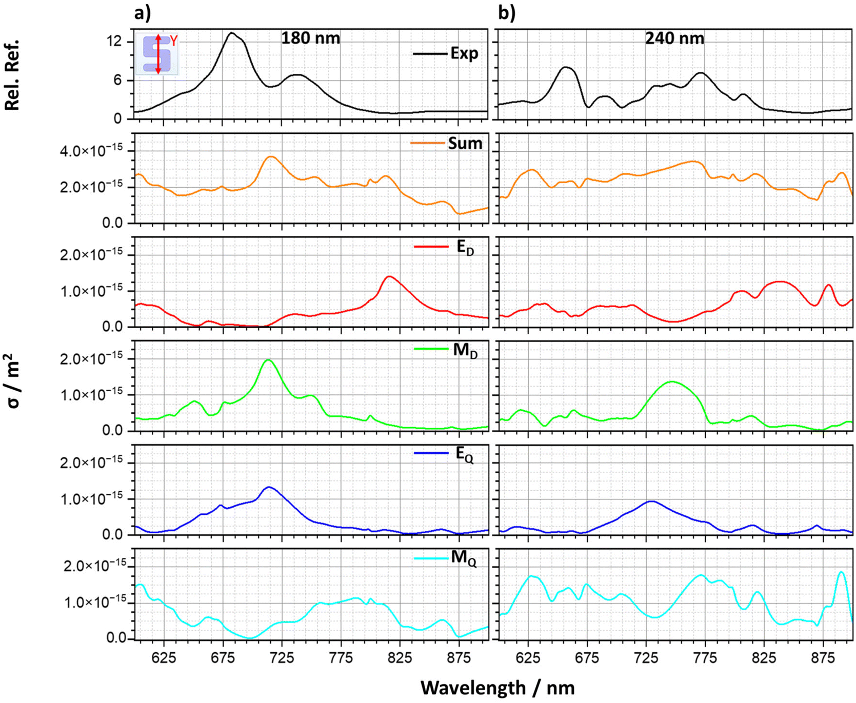 | ||
| Fig. 6 A comparison between the experimental reflectance (black) and the total scattering cross section (and individual contributions) for a RH structure at (a) 180 nm and (b) 240 nm thickness, under y-polarised LPL. | ||
 | ||
| Fig. 7 A comparison between the experimental reflectance and the total scattering cross section (and individual contributions) for a RH structure at (a) 180 nm and (b) 240 nm thickness, under x-polarised LPL. Note the increased scale of the 240 nm MQ data. | ||
For the y-polarisation, the total scattering cross section shows qualitative agreement with the experimental reflectance for both sample heights in terms of peak shape. The dominant contribution towards peaks A and B is shown to be of MD character; peak A also has a significant EQ contribution. These multipole assignments agree with the field plots, where |H| intensities (the MD resonance) are accompanied by circulating electric currents (EQ). The multipolar resonances can be seen to red shift with increasing height of the silicon. There is also a significant change in the magnetic quadrupole contribution for the thicker sample.
For the x-polarisation data, there is reasonable agreement between the experimental reflectance and the total scattering cross-section. The increase in reflectance for the 240 nm sample is repeated in the total scattering cross section, with a large increase contribution of the MQ.
Overall, the total scattering calculated from the numerical simulations captures the general shapes of the reflectance spectra, although the relative peak intensities are not in as good agreement. This is likely a result of the scattering components being calculated in all directions, opposed to directional scattering (reflectance) measured in experiment and simulation. High index dielectric materials such as silicon produce a magnetic (first) dipolar resonance, in contrast to plasmonic materials, when excited by incident light.15 This supports the dominant behaviour displayed by the structures being MD at lower sample thicknesses. The more dominant MQ contributions for the thicker sample can be rationalised by considering that the magnetic components of the resonances are parallel to the incident light excitation, therefore, as the silicon depth is increased, MQ is better supported across the height of the structures.17
The overall changes in the reflectance behaviour with increasing silicon thickness can be attributed to two sources. Those being a red shifting of resonances and significant increase in MQ contribution on increasing the thickness of the silicon to 240 nm.
Optical rotation from Stokes polarimetry
ORD spectra were obtained using a Stokes polarimeter for the samples for both incident polarisations, shown in Fig. 8.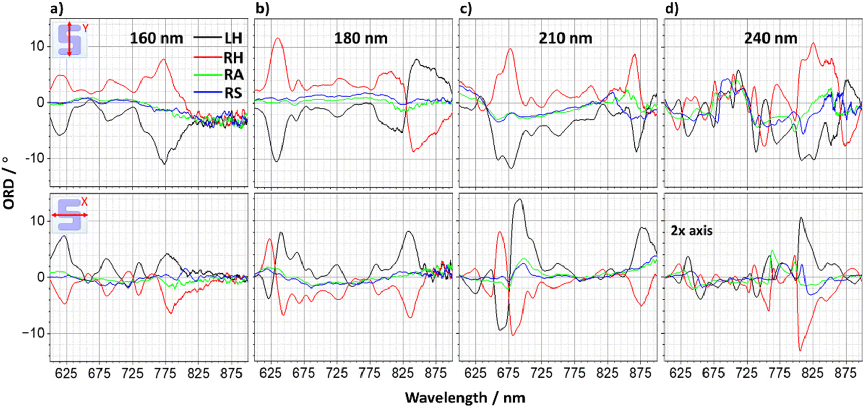 | ||
| Fig. 8 Experimental ORD spectra obtained for y-(top) and x-polarised (bottom) LPL for 160–240 nm sample heights, (a)–(d). Note the increased scale of the 240 nm data. | ||
The line shapes change substantially with silicon thickness. Spectra from enantiomorphic arrays display approximately equal and opposite behaviour, whilst the racemic versions show no significant resonances, behaviour consistent with optical activity. However, significantly, the line shape of the spectra depends strongly on the incident polarisation of light. This is inconsistent with an optical active chiral response, clearly indicating the optical rotation is dominated by the birefringent nature of the samples.
The birefringent origin of the observed optical rotation is further confirmed by the non-reciprocal ORD responses, Fig. 9a–d. The line shapes of the reflectance spectra are independent of the direction of propagation of the incident light. In contrast, the ORD resonances undergo both a change in sign and line shape when the sample is flipped around. This ORD behaviour is inconsistent with optical activity, which is reciprocal,27 and therefore must be dominated by the birefringence of the sample.
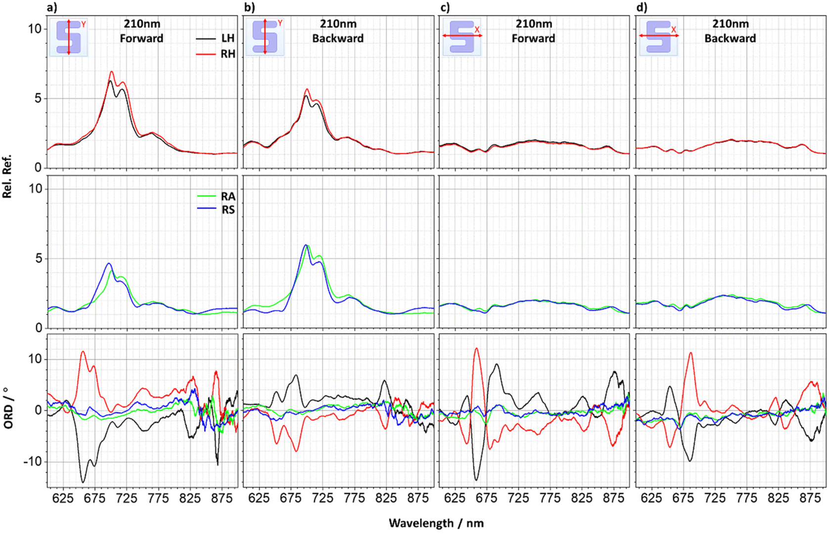 | ||
| Fig. 9 Experimental y-polarised (a) forwards, (b) backwards and x-polarised (c) forwards and (d) backwards illuminated reflectance and ORD measurements for a 210 nm sample. | ||
Mueller matrix polarimetry
Stokes polarimetry, which is predominately used to study chiroptical responses of metamaterials, cannot decouple chiroptical and birefringent effects. This requires a complete characterisation of a sample's interaction with light using Mueller Matrix Polarimetry (MMP).28 Consequently, we have used MMP to collect circular dichroism/birefringence (CD/CB), linear dichroism/birefringence (LD/LB), linear dichroism/birefringence at ±45° (LD′/LB′) and g-factor from 210 nm thick samples (see ESI S8–10†). The MMP setup is housed at beamline B23 at Diamond Light Source Ltd, and is described elsewhere.29 For brevity, only CD, LB, LD′ and a simulated CD spectra are shown in Fig. 10.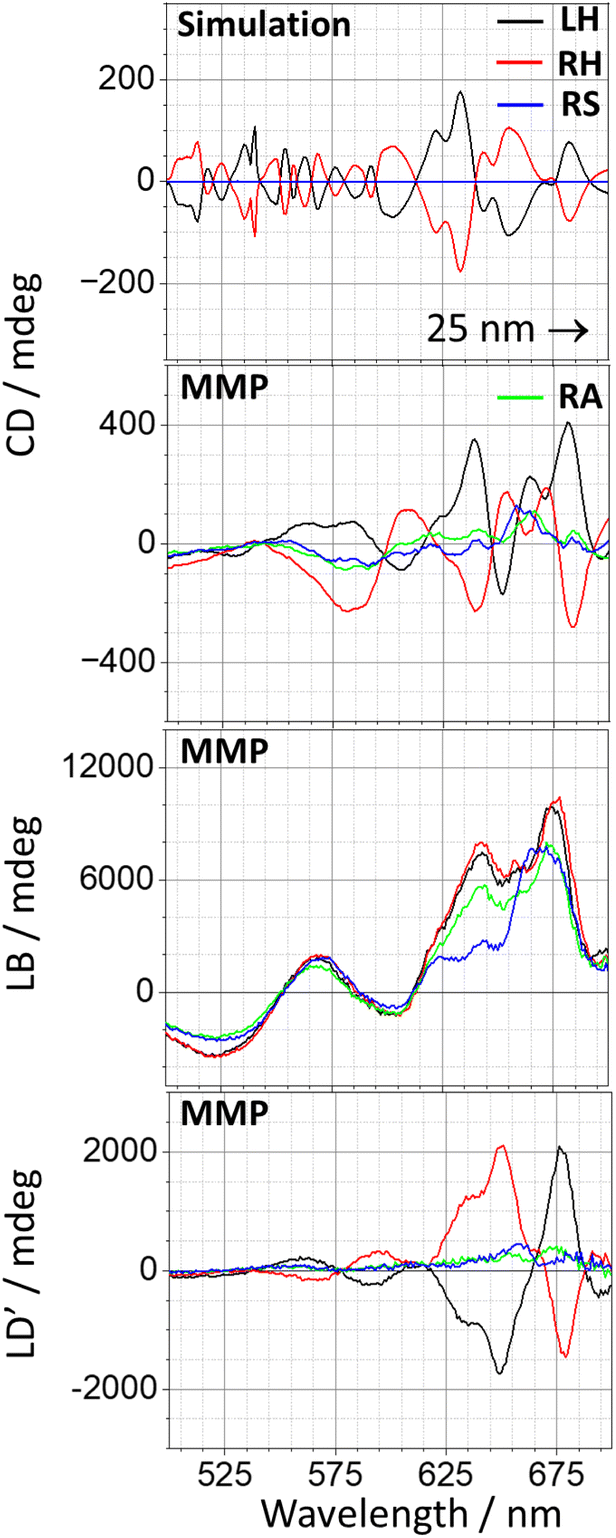 | ||
| Fig. 10 A comparison between simulated CD and MMP measured CD, LB and LD′ for a 210 nm sample. The MMP CD data has been smoothed to aid comparison. | ||
As would be expected based on the Stokes polarimetry data, the birefringent response is the dominant contribution, being ∼ one order of magnitude larger than the optical activity measured by CD.
The CD spectra collected from LH and RH metasurfaces are approximately equal and opposite, with the RA and RS spectra consistently at the midpoint between the two. The simulated CD spectra is red shifted by 25 nm to account for the typical red shift associated with the idealised models, to aid comparison with experiment. There is reasonable agreement between simulated and experimental data, albeit that as expected, the former is more resolved. Experimentally, between 645–675 nm the spectra lie on an underlying background, which mimics relatively closely the CD response from RA and RS arrays. The LH/RH spectra would otherwise be expected to cross 0 mdeg at 675 nm. When this is taken into account the simulation and experiment spectra are in good agreement. At lower wavelengths, the broad experimental peak across 575 nm appears as an oscillating feature in the simulation, which shows a positive (negative) mdeg bias for the LH (RH) array. Using a curve smoothing function over this wavelength range on the simulated spectra, which previously has been used to mimic the effects of structural heterogeneity, would improve the level of agreement with experiment.30 The observed levels of CD are of a similar magnitude to plasmonic 2D chiral geometries18,31 and are much greater those produced from colloidal nanoparticle arrangements, however the latter is advantageously more suitable for mass production.32,33
Although the spectral line shapes differ, the resonances associated with optical activity and birefringence do occur in similar positions. The most intense features occur within the 625–685 nm wavelength range in which the EQ and MD are located. The anisotropic properties of these modes are the origins of the birefringent resonances, however, optical activity has different origins. For isotropic chiral media, optical activity stems from the ED·MD cross term, which has a small magnitude and is the cause of the inherent weakness of chiroptical responses in solution phase. For anisotropic media ED·EQ is non-zero and can make a significant contribution to optical activity, particularly in the case of metamaterials where large field gradients enhance its influence.34,35 Consequently, increasing the thickness of the silicon structures alters the optical activity because it shifts both the ED and EQ modes and hence changes the magnitude of the cross-terms.
Optical chirality
The chiral asymmetry of near fields can be parameterised using the optical chirality parameter (C),36 which are typically normalised to the value of that of a helicity of circularly polarised light (in this current study, right-circularly polarised light (RCPL)). Near fields generated by scattering of even LPL from chiral nanostructures can generate near fields which in localised regions of space have significantly higher chiral asymmetries than circularly polarised light. This property is sometimes referred to as superchirality.18,37 The levels of optical chirality of near fields generated by x- and y-polarised light as a function of silicon thickness have been derived from numerical simulations. Fig. 11 shows the volume averaged optical chirality calculated from the structure and surrounding volume above the substrate.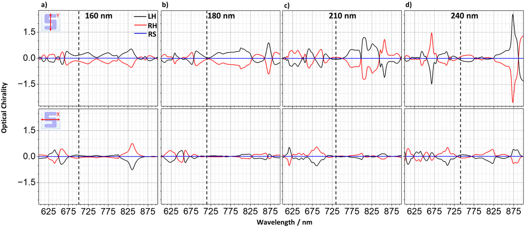 | ||
| Fig. 11 Volume averaged optical chirality values for 160–240 nm sample heights, (a)–(d), calculated from the structures and surrounding volumes, under y- and x-polarised LPL, normalised against RCPL. Dashed lines correspond to peak A. | ||
As expected of enantiomorphic structures, the optical chirality is equal and opposite between the LH and RH forms, the net contributions of which cancel in the case of the RS array. A notable aspect of the optical chirality is that the sign is wavelength dependent and is not solely determined by the handedness of the structure. Peaks in optical chirality corelate to wavelength regions where one would expect to find ED, MD and EQ resonances. Indeed, the largest peaks in optical chirality are observed for y-polarised incident light which produces stronger ED, MD and EQ resonances, than the equivalent ones for x-polarised illumination.
Maps shown in Fig. 12 illustrate the spatial distribution of the chiral asymmetries of the near fields at wavelengths corresponding to peak A resonances, shown as dashed lines in the volume averaged optical chirality plot. These maps show equal and opposite behaviour expected of enantiomorphic structures. Fields within the silicon structures show high levels of chiral asymmetries (i.e., superchiral). However, there are relatively strong superchiral fields that exist near the surface of the structures and between adjacent arms, in the case of the y-polarised illumination; fields which could potentially be exploited for chiral sensing.
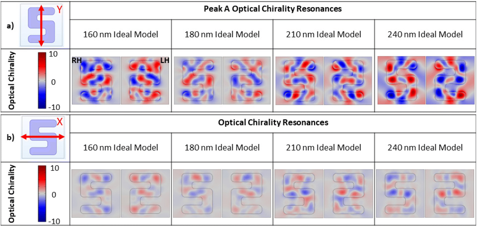 | ||
| Fig. 12 Optical chirality maps for LH and RH structures at each sample height corresponding to dashed lines of previous figure, under (a) y- and (b) x-polarised LPL, normalised against RCPL. | ||
Conclusions
We have presented chiral silicon metasurfaces which display strong optical rotation properties that are dependent on the height of the constituent nanostructures. The inherent birefringence of the structure is the dominant contribution to optical rotation, being an order of magnitude greater than the chirality derived optical activity. Using Mueller matrix polarimetry, the birefringent and optical activity contributions could be decoupled. The thickness dependence of the optical rotation could be understood through a multipole decomposition based on numerical simulations. The change in behaviour for the thickest sample was attributed to a combination of the resonance shifting as well as a large increase in magnetic quadrupole contribution. This change in multipolar character is facilitated by the greater ability of the thicker sample to sustain multipolar resonances that are supported across the height of the structures. The arrays were found to generate large enhancements of optical chirality in and around the nanostructures, which was also found to increase with sample height. In a broader context the present study has implications for the use of dielectric metasurfaces in applications such as enantiomeric/biomacromolecular detection. It illustrates the potential of birefringent effects to dominate the response from metasurfaces obtained using ubiquitous Stokes polarimetry methodologies. Non-reciprocity has often been falsely assumed to be the expected response from chiral planar metasurfaces formed from structures which in free space have horizontal mirror planes. Using MMP measurements clearly illustrates that such non-reciprocity originates from birefringence. Finally, using the multipolar analysis we illustrate how ED·EQ cross-term contributes both to the optical activity displayed by the structures and the enhanced chiral asymmetry of the near fields.Methodology
Sample fabrication
Samples were fabricated in the James Watt Nanofabrication Centre (JWNC). The s-structures were fabricated using an electron beam lithography process. Quartz glass slides were cleaned under ultrasonic agitation in acetone, methanol, and isopropyl alcohol (AMI) for 5 min each, dried under N2 flow and exposed to O2 plasma for 5 min at 100 W. Amorphous silicon was deposited on the substrates through PECVD with a SPTS Delta tool. The samples were cleaned as before, with a 1 min lower power 60 W plasma clean. A PMMA resist bilayer was then spun at 4000 rpm for 1 min and baked at 180 °C for 5 min between spins. A 10 nm aluminium conducting layer was evaporated on the substrates using a PLASSYS MEB 550s evaporator. Patterns were designed on the CAD software L-Edit and written by a Raith EBPG 5200 electron beam tool operating at 100 kV. The Al was removed in CD-26 and the resist developed in 3![[thin space (1/6-em)]](https://www.rsc.org/images/entities/char_2009.gif) :1 MIBK:IPA solution at 23.2 °C for 1 min, rinsed in IPA for 5 seconds and then RO water before drying under N2 flow. A 50 nm nichrome etch mask was then evaporated onto the sample prior to a lift-off procedure in acetone at 50 °C overnight, with the sample agitated to remove all remaining resist and excess metal. The silicon was etched using an STS tool with a custom recipe of C4F8/SF6 90/30 sccm, 600 W, 9.8 mTorr, 20 °C for 3 minutes. The NiCr etch mask was removed by immersion in chromium etchant and 60% Nitric acid. The process was completed with a final AMI and low power plasma cleaning.
:1 MIBK:IPA solution at 23.2 °C for 1 min, rinsed in IPA for 5 seconds and then RO water before drying under N2 flow. A 50 nm nichrome etch mask was then evaporated onto the sample prior to a lift-off procedure in acetone at 50 °C overnight, with the sample agitated to remove all remaining resist and excess metal. The silicon was etched using an STS tool with a custom recipe of C4F8/SF6 90/30 sccm, 600 W, 9.8 mTorr, 20 °C for 3 minutes. The NiCr etch mask was removed by immersion in chromium etchant and 60% Nitric acid. The process was completed with a final AMI and low power plasma cleaning.
Reflectance measurements
Substrates were placed in a custom-printed sample holder, with a FastWell Silicone seal and clear borosilicate glass slide above it. The nanoarrays were immersed in PBS by injecting the buffer into the holder cavity. The sample was secured on the stage of a custom built stokes polarimeter. The incident polarisation was altered using a linear polariser and ORD was collected by measuring intensities at four angles of the analyser, which was rotated between 0°, 45°, 90° and 135°. Reflectance data was obtained with the analyser at 0°.Mueller matrix polarimetry
Samples measured for MMP were prepared in the same manner as for the Stokes polarimeter. Two pairs of photoelastic modulators either side of the sample act as a polarisation state generator and polarisation state analyser, allowing for production and measurement of all light states required to obtain the 16 Mueller matrix elements.Numerical simulations
Simulations were carried out using commercial finite element analysis software, COMSOL Multiphysics v6.1 (Wave optics module). The nanostructure is surrounded by a cuboid representing a unit cell, with the x and y dimensions defining the periodicity of the metamaterial, as calculated from AFM images. The z dimensions of the cell are sufficiently large (≥λmax/2) that near-fields generated by the nanostructures do not extend to any integration surfaces above the structure, the total height of the cell is 1800 nm. The unit cell is split up into domains of varying thickness. The top and bottom 200 nm domains are perfectly matched layers (PMLs) which absorb all reflections from the nanoparticle. The boundary adjacent to the upper PML is the excitation port, from which incident light originates and its polarization is specified. Reflection intensity is also calculated at this port. The silicon structure is near the centre of the cuboid. The boundary adjacent to the lower PML is the outgoing port.Author contributions
The manuscript was written through contributions of all authors. All authors have given approval to the final version of the manuscript.Conflicts of interest
There are no conflicts to declare.Acknowledgements
The authors acknowledge financial support from the Engineering and Physical Sciences Research Council (EP/P00086X/1 and EP/M024423/1). Technical support from the James Watt Nanofabrication Centre (JWNC) and Diamond Light Source Ltd is acknowledged. DKM was awarded a studentship by the EPSRC. M. K. acknowledges the Leverhulme Trust for the award of a Research Fellowship.References
- J. García-Guirado, M. Svedendahl, J. Puigdollers and R. Quidant, Enhanced Chiral Sensing with Dielectric Nanoresonators, Nano Lett., 2020, 20, 585–591 CrossRef.
- E. Mohammadi, et al., Nanophotonic Platforms for Enhanced Chiral Sensing, ACS Photonics, 2018, 5, 2669–2675 CrossRef CAS.
- E. Hendry, R. V. Mikhaylovskiy, L. D. Barron, M. Kadodwala and T. J. Davis, Chiral Electromagnetic Fields Generated by Arrays of Nanoslits, Nano Lett., 2012, 12, 3640–3644 CrossRef CAS PubMed.
- J. Wade, et al., Natural optical activity as the origin of the large chiroptical properties in π-conjugated polymer thin films, Nat. Commun., 2020, 11, 6137 CrossRef CAS.
- J. Crassous, et al., Materials for chiral light control, Nat. Rev. Mater., 2023, 8, 365–371 CrossRef.
- K. Yao and Y. Liu, Plasmonic metamaterials, Nanotechnol. Rev., 2014, 3, 177–210 CAS.
- S. Jahani and Z. Jacob, All-dielectric metamaterials, Nat. Nanotechnol., 2016, 11, 23–36 CrossRef CAS PubMed.
- Y. Hu, et al., All-dielectric metasurfaces for polarization manipulation: principles and emerging applications, Nanophotonics, 2020, 9, 3755–3780 CrossRef.
- A. Ali, A. Mitra and B. Aïssa, Metamaterials and Metasurfaces: A Review from the Perspectives of Materials, Mechanisms and Advanced Metadevices, Nanomaterials, 2022, 12, 1027 CrossRef CAS.
- S. Efrima, Raman optical activity of molecules adsorbed on metal surfaces: Theory, J. Chem. Phys., 1985, 83, 1356–1362 CrossRef CAS.
- A. I. Kuznetsov, A. E. Miroshnichenko, Y. H. Fu, J. Zhang and B. Luk'yanchuk, Magnetic light, Sci. Rep., 2012, 2, 492 CrossRef.
- U. Zywietz, A. B. Evlyukhin, C. Reinhardt and B. N. Chichkov, Laser printing of silicon nanoparticles with resonant optical electric and magnetic responses, Nat. Commun., 2014, 5, 3402 CrossRef.
- P. A. Dmitriev, et al., Laser fabrication of crystalline silicon nanoresonators from an amorphous film for low-loss all-dielectric nanophotonics, Nanoscale, 2016, 8, 5043–5048 RSC.
- G. Mie, Beiträge zur Optik trüber Medien, speziell kolloidaler Metallösungen, Ann. Phys., 1908, 330, 377–445 CrossRef.
- M. L. De Marco, et al., Silicon-Based Dielectric Metamaterials: Focus on the Current Synthetic Challenges, Angew. Chem., Int. Ed., 2018, 57, 4478–4498 CrossRef PubMed.
- A. B. Evlyukhin, et al., Demonstration of Magnetic Dipole Resonances of Dielectric Nanospheres in the Visible Region, Nano Lett., 2012, 12, 3749–3755 CrossRef CAS.
- C. Liu, et al., Characteristics of electric quadrupole and magnetic quadrupole coupling in a symmetric silicon structure, New J. Phys., 2020, 22, 23018 CrossRef.
- E. Hendry, et al., Ultrasensitive detection and characterization of biomolecules using superchiral fields, Nat. Nanotechnol., 2010, 5, 783 CrossRef CAS PubMed.
- C. Gilroy, D. J. P. Koyroytsaltis-McQuire, N. Gadegaard, A. S. Karimullah and M. Kadodwala, Superchiral hot-spots in “real” chiral plasmonic structures, Mater. Adv., 2022, 3, 346–354 RSC.
- Q. Zhao, J. Zhou, F. Zhang and D. Lippens, Mie resonance-based dielectric metamaterials, Mater. Today, 2009, 12, 60–69 CrossRef CAS.
- G. W. Castellanos, P. Bai, G. Rivas and J. Lattice, resonances in dielectric metasurfaces, J. Appl. Phys., 2019, 125, 213105 CrossRef.
- J. D. Jackson, Classical electrodynamics, 1999 Search PubMed.
- A. B. Evlyukhin, T. Fischer, C. Reinhardt and B. N. Chichkov, Optical theorem and multipole scattering of light by arbitrarily shaped nanoparticles, Phys. Rev. B, 2016, 94, 205434 CrossRef.
- A. B. Evlyukhin and B. N. Chichkov, Multipole decompositions for directional light scattering, Phys. Rev. B, 2019, 100, 125415 CrossRef CAS.
- A. B. Evlyukhin, C. Reinhardt, A. Seidel, B. S. Luk'yanchuk and B. N. Chichkov, Optical response features of Si-nanoparticle arrays, Phys. Rev. B: Condens. Matter Mater. Phys., 2010, 82, 45404 CrossRef.
- A. B. Evlyukhin, C. Reinhardt and B. N. Chichkov, Multipole light scattering by nonspherical nanoparticles in the discrete dipole approximation, Phys. Rev. B: Condens. Matter Mater. Phys., 2011, 84, 235429 CrossRef.
- O. Arteaga, et al., Relation between 2D/3D chirality and the appearance of chiroptical effects in real nanostructures, Opt. Express, 2016, 24, 2242–2252 CrossRef CAS PubMed.
- O. Arteaga and B. Kahr, Mueller matrix polarimetry of bianisotropic materials [Invited], J. Opt. Soc. Am. B, 2019, 36, F72–F83 CrossRef CAS.
- R. Hussain, T. Jávorfi and G. Siligardi, CD Imaging at High Spatial Resolution at Diamond B23 Beamline: Evolution and Applications, Front. Chem., 2021, 9, 616928 CrossRef CAS PubMed.
- C. Ciracì, et al., Impact of Surface Roughness in Nanogap Plasmonic Systems, ACS Photonics, 2020, 7, 908–913 CrossRef.
- D. J. P. Koyroytsaltis-McQuire, et al., Detecting Antibody–Antigen Interactions with Chiral Plasmons: Factors Influencing Chiral Plasmonic Sensing, Adv. Photonics Res., 2022, 3, 2100155 CrossRef.
- A. Ben-Moshe, et al., Enantioselective control of lattice and shape chirality in inorganic nanostructures using chiral biomolecules, Nat. Commun., 2014, 5, 4302 CrossRef CAS.
- O. Ávalos-Ovando, et al., Chiral Bioinspired Plasmonics: A Paradigm Shift for Optical Activity and Photochemistry, ACS Photonics, 2022, 9, 2219–2236 CrossRef.
- R. Tullius, et al., “Superchiral” Spectroscopy: Detection of Protein Higher Order Hierarchical Structure with Chiral Plasmonic Nanostructures, J. Am. Chem. Soc., 2015, 137, 8380–8383 CrossRef CAS.
- I. P. Theron and J. H. Cloete, The electric quadrupole contribution to the circular birefringence of nonmagnetic anisotropic chiral media: a circular waveguide experiment, IEEE Trans. Microwave Theory Tech., 1996, 44, 1451–1459 CrossRef.
- Y. Tang and A. E. Cohen, Optical Chirality and Its Interaction with Matter, Phys. Rev. Lett., 2010, 104, 163901 CrossRef.
- Y. Tang and A. E. Cohen, Enhanced Enantioselectivity in Excitation of Chiral Molecules by Superchiral Light, Science, 2011, 332, 333 CrossRef CAS PubMed.
Footnote |
| † Electronic supplementary information (ESI) available. See DOI: https://doi.org/10.1039/d3nr05285k |
| This journal is © The Royal Society of Chemistry 2024 |