
Effects of thermal annealing on analog resistive switching behavior in bilayer HfO2/ZnO synaptic devices: the role of ZnO grain boundaries†
Yeong-Jin
An‡
a,
Han
Yan‡
 a,
Chae-min
Yeom
a,
Jun-kyo
Jeong
a,
Sunil Babu
Eadi
a,
Hi-Deok
Lee
*a and
Hyuk-Min
Kwon
*b
a,
Chae-min
Yeom
a,
Jun-kyo
Jeong
a,
Sunil Babu
Eadi
a,
Hi-Deok
Lee
*a and
Hyuk-Min
Kwon
*b
aDepartment of Electronics Engineering, Chungnam National University, Daejeon, 34134, Republic of Korea. E-mail: hdlee@cnu.ac.kr
bDepartment of Semiconductor Processing Equipment, Semiconductor Convergence Campus of Korea Polytechnic College, Anseong, Kyunggi-Do 17550, Republic of Korea. E-mail: hmkwon@kopo.ac.kr
First published on 20th January 2024
Abstract
The effects of thermal annealing on analog resistive switching behavior in bilayer HfO2/ZnO synaptic devices were investigated. The annealed active ZnO layer between the top Pd electrode and the HfO2 layer exhibited electroforming-free resistive switching. In particular, the switching uniformity, stability, and reliability of the synaptic devices were dramatically improved via thermal annealing at 600 °C atomic force microscopy and X-ray diffraction analyses revealed that active ZnO films demonstrated increased grain size upon annealing from 400 °C to 700 °C, whereas the ZnO film thickness and the annealing of the HfO2 layer in bilayer HfO2/ZnO synaptic devices did not profoundly affect the analog switching behavior. The optimized thermal annealing at 600 °C in bilayer HfO2/ZnO synaptic devices dramatically improved the nonlinearity of long-term potentiation/depression properties, the relative coefficient of variation of the asymmetry distribution σ/μ, and the asymmetry ratio, which approached 1. The results offer valuable insights into the implementation of highly robust synaptic devices in neural networks.
1. Introduction
As the conventional von Neumann architecture causes slow calculation speed and high energy consumption, the demand for low-energy and highly adaptable computing has gradually increased with the development of big data, the Internet of Things, and artificial intelligence.1,2 Thus, extensive research has been conducted to enhance the efficiency of information processing under ultralow power consumption based on the imitation of the neuromorphic system of the human brain.3,4 The potential of neuromorphic computing has attracted interest for the development of various materials and devices.5 Prezioso et al. (2018)6 proposed a memristive device based on a metal–organic framework that can emulate the plasticity of biological synapses. The device demonstrated high accuracy in recognizing handwritten digits and consumed considerably less power than conventional computing methods. Neuromorphic computing has become a promising method to achieve highly efficient data processing in which memristive devices are used owing to their simple structure, elevated integration, low power consumption, and analog conductance modulation.7–12 Digital memristive devices with abrupt resistive switching in which the active material is sandwiched between two electrodes have been widely studied for next-generation non-volatile memory applications.13 Digital memristive devices exhibit the formation and rupture of conduction filaments (CFs), indicating that filamentary digital memristive devices can be repeatedly switched with abrupt set/reset switching. On the contrary, analog memristive devices with gradual resistive switching can be modulated by applied electrical stimuli, similar to synapses that carry information from one neuron to another.14–16 The application of electrical stimuli can tune the internal resistance of the active material and improve conductivity, similar to synaptic weight potentiation. In addition, it is similar to synaptic weight depression in the conductance state of the active material, where the conductivity decreases continuously with increasing electrical reverse voltage.17 Interestingly, analog memristive devices with inherent ionic dynamics analogous to biological synapses show promising features in exploiting artificial synapses for brain-inspired neuromorphic computing. However, the mechanism of analog resistive switching has remained obscure as few studies have been performed on analog memristive devices.In digital memristive devices, transition metal oxides, mainly based on Al2O3,18 HfO2,19 TaOx,20 ZrO2,21 TiO2,22 and others, are used owing to their abrupt resistive switching upon the formation of a highly conductive path to realize high-performance memory devices. However, single-layer memristive devices with transition metal oxides suffer from uncontrolled filament formation, high switching voltage, and gradual change in conductance under bipolar resistive switching.23 The electroforming process is usually required to obtain stable resistive switching; however, it uses a much higher bias and may result in unpredictable resistance states, making it difficult to modulate resistive switching. An active-metal–oxide deposition technique was developed via the redox reaction of oxide-based materials, such as TiOx,24 TaOx,25 WOx,25 AlOx,26 HfOx,27 and PrxCa1−xMnO3 (PCMO),28 introduced between the transition metal oxide and the top electrode to significantly improve the resistive switching behavior. Recently, an electroforming-free process based on indium–gallium zinc oxide (IGZO) and zinc oxide (ZnO) has been proposed to modulate conductance during resistive switching.29 IGZO and ZnO films offer low cost, low deposition temperature, controllable electrical behavior, chemical stability, and electrochemical activity, leading to their application in neuromorphic computing.30 The conduction mechanism of the metal oxide film is related to the electrical migration of oxygen ions/vacancies in the switching film.31,32 However, the controllability of oxygen vacancies via thermal annealing is a major challenge, mainly because the oxygen vacancy concentration significantly affects the conductivity of the material.33,34 The redistribution of oxygen vacancies upon thermal annealing depends on the grain boundary size, duration, and the number of programming pulses, allowing memristive devices to mimic synaptic plasticity by exhibiting analog resistive switching characteristics.35,36 In particular, ZnO deposited by atomic layer deposition (ALD) usually forms a polycrystalline structure owing to a large lattice mismatch, indicating that its electric properties depend on microstructural characteristics.37 Thermal annealing affects ZnO film properties by modifying the interfacial structure of grain boundaries.38 A significant improvement in synaptic plasticity may be possible by employing the dependencies on the grain boundary of a geometrical functional scheme, which can inherently modulate ionic transfer dynamics in the active layer. In the set process, oxygen ions within transition metal oxides may migrate more readily to the top metal electrode along grain boundaries within the active layer in response to an electric field. The reset process of memristive devices decreases the conductance in the off state by removing the CF path through the grain boundary region of the active layer between the transition metal oxide and the top electrode.39 In addition, there is limited information about the characteristics of ZnO active layers in bilayer memristive devices, and little is known about the properties of grain boundaries in the ZnO active layer and how they impact synaptic functions in memristive devices.
In this work, we investigated the effects of thermal annealing on analog resistive switching behavior in bilayer HfO2/ZnO synaptic devices to mimic the functions of biological synapses. In particular, the nanocrystalline structure of active ZnO films in bilayer HfO2/ZnO synaptic devices was easily formed via thermal annealing, and its effects on the electroforming-free resistive switching behavior were evaluated. We verified the improved uniformity in VSET and VRESET distributions with the cycle number and on/off ratio. Atomic force microscopy (AFM) and X-ray diffraction (XRD) verified that the increase in annealing temperature caused grain boundary enlargement, which could improve diffusion paths for oxygen vacancies to control the conductance modulation. To verify the role of the film thickness and the annealed ZnO layer in the bilayer HfO2/ZnO structure, two synaptic devices comprising 6 nm single-layer HfO2 and bilayer HfO2/ZnO were fabricated without and with thermal annealing at 600 °C and compared. Consequently, the switching uniformity, stability, and reliability of bilayer HfO2/ZnO synaptic devices were optimized via thermal annealing at 600 °C.
2. Experimental procedure
The fabrication of synaptic memristive devices was performed after the thermal oxidation of silicon dioxide (SiO2, 300 nm) on a (100) silicon substrate. As shown in Fig. 1(a), Pt was deposited on a SiO2/Si substrate as the bottom electrode by an electron-beam evaporator. To better match the physical contact and electrical properties of the substrate with the bottom electrode, the adhesion between SiO2 and Pt layers and conductivity were improved by the deposition of a 10 nm Ti layer. An ALD system at a chamber temperature of 200 °C was used to deposit a 3 nm HfO2 layer using tetrakis(ethylmethylamino)Hafnium (TEMAH), Hf[N(CH3)(C2H5)]4 and source precursors in H2O on the bottom electrode. Then, a 3 nm ZnO layer was deposited by ALD using DEZn (diethylzinc, Zn(C2H5)2) and source precursors in H2O at a chamber temperature of 80 °C. Consequently, the samples were annealed in a quartz tube furnace at 400 °C, 500 °C, 600 °C, and 700 °C for 1 h in an N2 ambient. After cooling the annealed samples, the pattern fabrication of the top electrode was conducted using a negative photoresist by photolithography. Finally, 150 nm Pd was deposited using a radio frequency sputtering system as the top electrode in an Ar environment, and memristive devices with a crossbar structure were formed by the lift-off process. Cross-sectional high-resolution transmission electron microscopy (HRTEM) and energy dispersive X-ray spectroscopy (EDS) images of bilayer HfO2/ZnO synaptic devices were shown in Fig. 1(b). The physical thickness of bilayer HfO2/ZnO synaptic devices was measured by HRTEM, which was 3.94 nm of HfO2 and 3.17 nm of ZnO2, respectively, as shown in Fig. 1(b). Notably, all samples were fabricated at the same time to minimize variations in the devices due to the fabrication process, such as the deposition of resistive switching materials and bottom/top metal electrodes. The crystal structure and microstructure of ZnO films were characterized using XRD and AFM. The scanning area used in AFM was 2 × 2 μm.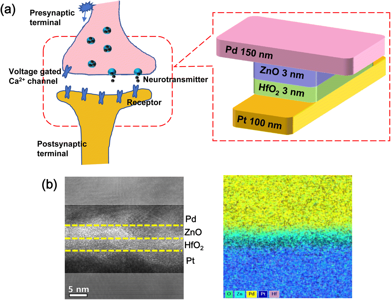 | ||
| Fig. 1 (a) Schematic illustration of neurotransmission processes in a biological synapse and a 3-dimensional (3D) crossbar structure with a bilayer HfO2/ZnO synaptic device (artificial synapse), where the top Pd metal electrode mimics pre-synaptic neurons, and the bottom Pt metal electrode emulates post-synaptic neurons, (b) cross-sectional high-resolution transmission electron microscopy (HRTEM) and energy dispersive X-ray spectroscopy (EDS) images of bilayer HfO2/ZnO synaptic devices. | ||
Electrical measurements were performed using a Keysight B1500A semiconductor device analyzer to evaluate analog resistive switching characteristics and learning properties with pulse trains. All electrical measurements were obtained by applying a voltage to the top Pd electrode while the bottom Pt electrode was grounded. Synaptic functions in bilayer HfO2/ZnO synaptic devices were measured by Keysight B1530A with a waveform generator/fast measurement unit. For learning properties with pulse trains, all pulses were applied across the synaptic devices through the B1530 arbitrary waveform generator, and the currents were simultaneously monitored using the B1500 source measurement unit. To analyze the synaptic plasticity behavior of bilayer HfO2/ZnO synaptic devices, 100 pulses were applied, respectively, and the current was measured after each stimulation pulse.
3. Results and discussion
3.1. Surface morphology and crystallization
To confirm the effect of thermal annealing on grain boundaries, the surface morphologies of ZnO films upon thermal annealing in bilayer HfO2/ZnO synaptic devices were investigated by AFM, as shown in Fig. 2. In addition, AFM was used to visualize grain boundaries in nanocrystalline films.40 Variations in surface roughness were indicated by the root mean square (Rq or Rrms) and average roughness (Ra). The Rq value of the HfO2/ZnO interface in the as-deposited film was 0.72 ± 0.2 nm as shown in Fig. 2(a).41 The roughness parameters reduced when the annealing temperature increased from 400 °C to 700 °C, as shown in Fig. 2(b–e). Based on the AFM results, the dependence of the roughness parameters of ZnO films on annealing temperature was revealed, as shown in Fig. 2(f). The roughness parameters significantly increased for the ZnO films annealed at temperatures above 600 °C, which implies an increase in the ZnO grain size. At high temperatures, Zn and O atoms in ZnO films have enough activation energy for the internal migration process to complete the crystal lattice.42 Grain coalescence and re-growth in ZnO films at high temperatures are attributed to the increased grain size and reduced the grain boundary density because grains with low surface energies merge with neighboring grains and form large-size grains at high temperatures. Simultaneously, pore coalescence was observed in the AFM images of the ZnO films annealed at 600 °C and 700 °C.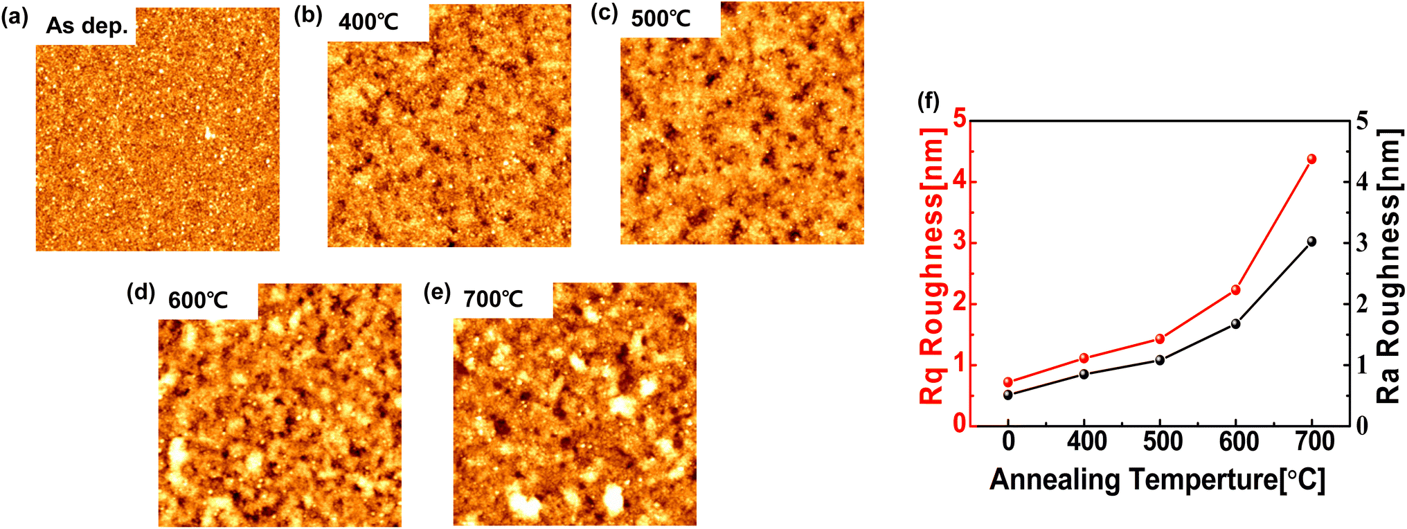 | ||
| Fig. 2 AFM surface topography images of ZnO films in bilayer HfO2/ZnO synaptic devices (a) without thermal annealing, (b) with thermal annealing at 400 °C, (c) 500 °C, (d) 600 °C, and (e) 700 °C. (f) Dependence of the root mean square (Rq or Rrms) and average roughness (Ra) of ZnO films on thermal annealing. | ||
To investigate the crystalline phase formation, HfO2/ZnO films were analyzed upon thermal annealing using XRD, as shown in Fig. 3. Actually, the thickness of the active ZnO layer increased from 3 nm to 10 nm to examine the tendency of crystallization because it was difficult to analyze broad diffraction peaks and low signal-to-noise ratios below 10 nm (see Fig. S1(a)†). The primary growth direction of ZnO is generally known as the (0001) direction in the hexagonal prism crystal structure because the (0001) plane has the lowest surface free energy.43 The crystal orientation of the ZnO film was favored in the Z-axis direction and appeared in the (002) crystal plane. The diffraction peaks of the HfO2/3 nm ZnO films on annealing temperature were not observed in the XRD results (see Fig. S1(b)†), indicating the formation of amorphous and/or nanocrystalline structures in ZnO deposited samples. When the sample is placed at a high temperature, sufficient diffusion activation energy is obtained to penetrate the lattice point, and grains with low surface energies merge with neighborhood grains and grow large in size. All samples exhibit a common XRD peak at around 51°, which originates from the Si substrate.44 Among the 10 nm ZnO diffraction peaks, 2θ angles of 31.9°, 34.4°, and 36.4° corresponded to the (100), (002), and (101) planes of ZnO (ICSD 31052), implying that the ZnO films were strongly oriented in the Z-axis direction. The obtained XRD diffraction peaks agreed well with the standard diffraction peaks of ZnO. When the annealing temperature increased from 400 °C to 700 °C, the intensity of all ZnO diffraction peaks increased significantly, as shown in Fig. 3(a). In addition, the diffraction peaks of HfO2 films were not found upon thermal annealing, indicating that the HfO2 films had a polycrystalline structure below 700 °C.
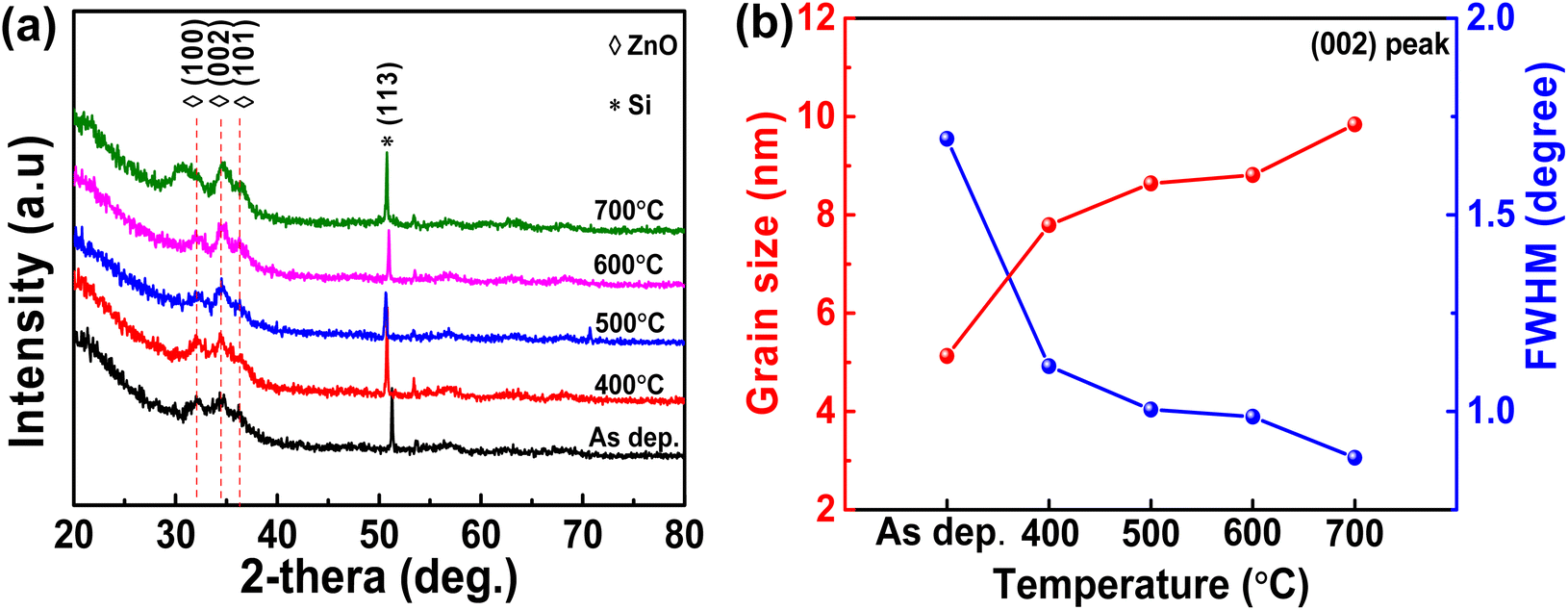 | ||
| Fig. 3 (a) X-Ray diffraction spectra of HfO2/ZnO films without and with thermal annealing from 400 °C to 700 °C. (b) Dependence of the full width at half maximum (FWHM) and average grain size of HfO2/ZnO films on annealing temperature. | ||
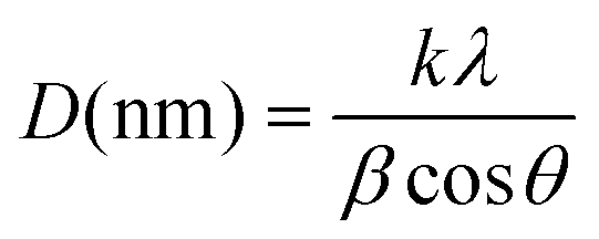
To analyze the thickness and grain size of polycrystalline films as a function of annealing temperature, the average polycrystalline sizes were estimated using the Debye–Scherrer equation,
 | (1) |
![[thin space (1/6-em)]](https://www.rsc.org/images/entities/char_2009.gif) =1.5406 Å), and β is the peak width of the diffraction peak profile at half maximum resulting from the crystallite size in radians. k is a dimensionless shape factor, with a typical value of approximately 0.9, and θ is the Bragg diffraction angle.45,46
=1.5406 Å), and β is the peak width of the diffraction peak profile at half maximum resulting from the crystallite size in radians. k is a dimensionless shape factor, with a typical value of approximately 0.9, and θ is the Bragg diffraction angle.45,46
Fig. 3(b) shows the dependence of the full width at half maximum (FWHM) and average grain size of HfO2/ZnO films on annealing temperature. As the annealing temperature increased, the FWHM reduced sharply and the average grain size increased, indicating the polycrystalline structure of ZnO films upon thermal annealing. The FWHM value is inversely proportional to the average grain size, which means that a lower FWHM and a larger grain size indicate better crystal quality. Consequentially, thermal energy generated by the annealing process facilitates atomic alignment in the plane with the lowest free surface energy, and nanocrystals aggregate after annealing to form larger crystallites, consistent with the AFM and XRD results.
3.2. Electrical characterization
To investigate device-to-device variation, Fig. 4(a) and (b) shows that the distribution and cumulative probability of the initial state during the electroforming process and low-resistance state (LRS) were measured in single-layer HfO2 and bilayer HfO2/ZnO synaptic devices without and with thermal annealing, where the initial state and LRS were extracted at a read voltage of ±0.3 V. Fig. S2† observes the I–V resistive switching cycle behaviors of 40 synaptic devices for single-layer HfO2 and bilayer HfO2/ZnO synaptic devices without and with thermal annealing. Electroforming HfO2 without and with thermal annealing and bilayer HfO2/ZnO synaptic devices without thermal annealing was conducted for the field-induced migration of oxygen vacancies in bilayer HfO2/ZnO films by voltage sweeping from 0 to 4 V, as shown in Fig. 4. A compliance current of 1 mA was set to prevent damage due to a sudden increase in current levels. Interestingly, the electroforming process did not affect the initial resistive switching behaviors of the bilayer HfO2/ZnO synaptic devices annealed at 400 °C, 500 °C, and 600 °C, as shown in Fig. 4. This implies that the electroforming-free process can generate defects or grain boundaries that act as high diffusion paths for oxygen vacancies in nanocrystalline ZnO films formed by thermal annealing.47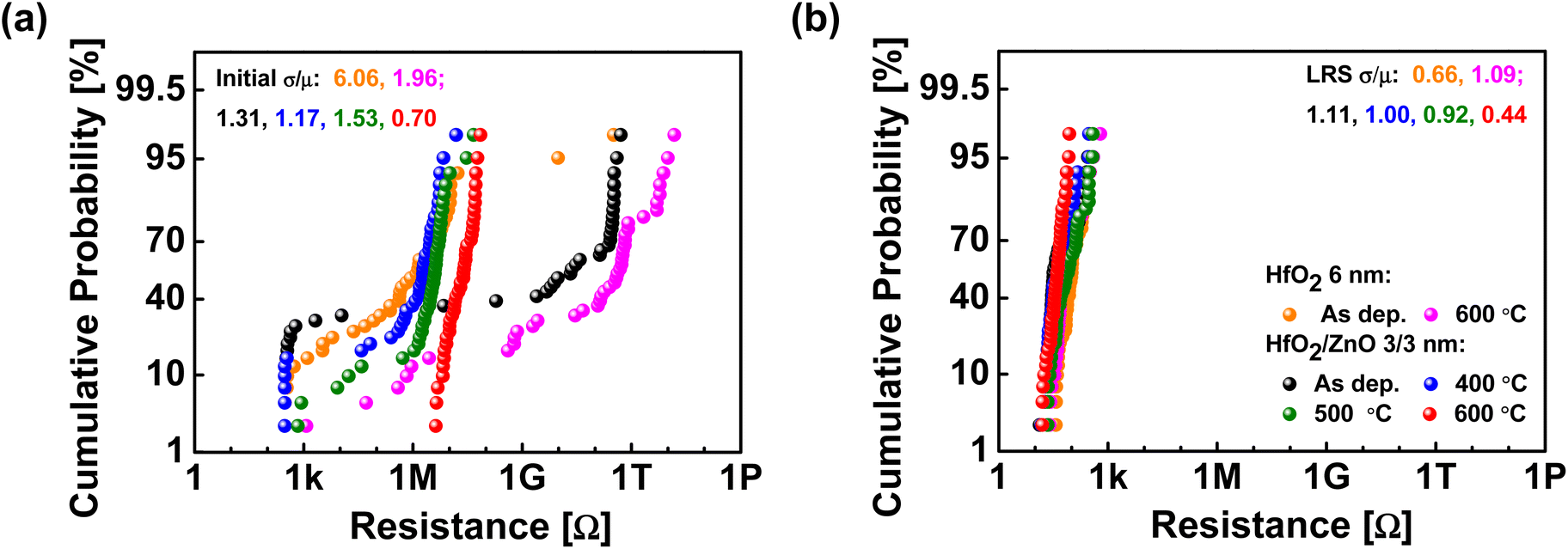 | ||
| Fig. 4 Distribution and cumulative probability of (a) the initial state during the electroforming process and (b) the low-resistance state (LRS) for single-layer HfO2 and bilayer HfO2/ZnO synaptic devices without and with thermal annealing, where the initial state and LRS were extracted at a read voltage of ±0.3 V. | ||
To investigate the effects of the formed grain boundaries on the resistance switching behavior, the typical current–voltage (I–V) switching of bilayer HfO2/ZnO synaptic devices without and with thermal annealing from 400 °C to 700 °C for 1 h in an N2 ambient is shown in Fig. 5(a–d). Abrupt (digital) and gradual (analog) switching behaviors were observed in bilayer HfO2/ZnO synaptic devices. However, bilayer HfO2/ZnO synaptic devices without thermal annealing show uniformity issues as the cycle number and on/off ratio varied. The uniformity is improved for bilayer HfO2/ZnO synaptic devices upon thermal annealing at 400 °C, 500 °C, and 600 °C, implying that the electroforming-free process can cause defects or grain boundaries that act as high diffusion paths for oxygen vacancies in the annealed nanocrystalline ZnO films. Bilayer HfO2/ZnO synaptic devices annealed at 700 °C no longer performed resistive switching because the crystallization of HfO2 and/or ZnO films became obvious, as shown in Fig. 5(e). The statistical results of the distribution and cumulative probability of the high-resistance state (HRS) and LRS in 40 consecutive I–V sweeps were obtained in bilayer HfO2/ZnO synaptic devices without and with thermal annealing, where the HRS and LRS were extracted at a read voltage of ±0.3 V, as shown in Fig. 5(f). The on/off ratio of our synaptic devices was approximately 103, confirming a clear resistance window and the improved resistance distribution of the HRS and LRS in 40 consecutive I–V sweeps upon thermal annealing at 600 °C. VSET and VRESET distributions in 40 consecutive I–V sweeps are repeatedly measured in bilayer HfO2/ZnO synaptic devices without and with thermal annealing, as shown in Fig. 6(a–d). The variability of VSET shows a significant improvement with increasing annealing temperature, while the distribution of VRESET exhibited uniformity with little deviation. The results showed that bilayer HfO2/ZnO synaptic devices annealed at 600 °C exhibited uniform VSET and VRESET distribution distributions, as well as gradual switching, which can be beneficial in binarized neural networks because the synaptic device response can be adjusted from cycle to cycle depending on the number of stimulations pulses.48
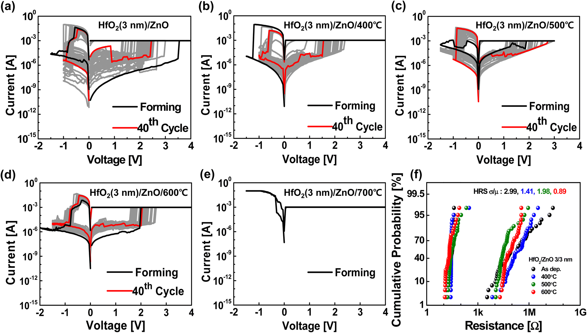 | ||
| Fig. 5 Typical current–voltage (I–V) resistive switching behavior of bilayer HfO2/ZnO synaptic devices (a) without and with thermal annealing at (b) 400 °C, (c) 500 °C, (d) 600 °C, and (e) 700 °C for 1 h in an N2 ambient. (f) Distribution and cumulative probability of the high-resistance state (HRS) and low-resistance state (LRS) in 40 consecutive I–V sweeps for bilayer HfO2/ZnO synaptic devices without and with thermal annealing, where the HRS and LRS were extracted at a read voltage of ±0.3 V. | ||
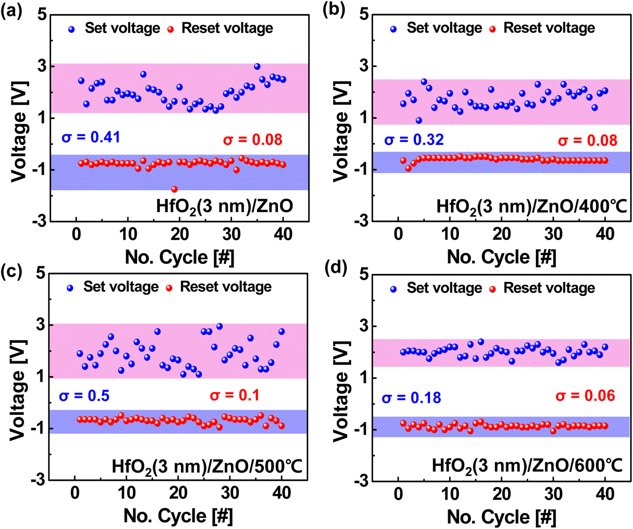 | ||
| Fig. 6 Obtained VSET and VRESET distributions for 40 consecutive I–V sweeps for bilayer HfO2/ZnO synaptic devices (a) without and with thermal annealing at (b) 400 °C, (c) 500 °C, and (d) 600 °C. | ||
To verify the improved role of the film thickness or the annealed ZnO layer in a bilayer HfO2/ZnO structure, we investigated the typical I–V switching behavior of 6 nm single-layer HfO2 and bilayer HfO2/ZnO synaptic devices without and with thermal annealing at 600 °C for 1 h in an N2 ambient (Fig. 7(a) and (b)). The uniformity of the resistive switching properties of the single-layer HfO2 synaptic device without and with thermal annealing at 600 °C further degraded because of the formation of a large number of conductive filaments. Also, after a bilayer 3 nm HfO2/3 nm ZnO structure with thermal annealing at 600 °C, the added ZnO films cause the cumulative probability and distribution degradation of HRS and LRS (see Fig. S3†). Importantly, the annealed ZnO film in a bilayer HfO2/ZnO structure improves the uniformity of the resistive switching properties.49,50 Therefore, because conductance values (the inverse of resistance values) are used as synaptic weights in binarized neural networks, the annealed ZnO films in bilayer HfO2/ZnO synaptic devices helped to improve the relatively high variability of the HRS. As previously mentioned, the AFM and XRD results revealed that the ZnO grain size increased upon annealing, which is consistent with the improvement in the resistance switching properties with annealing temperature.
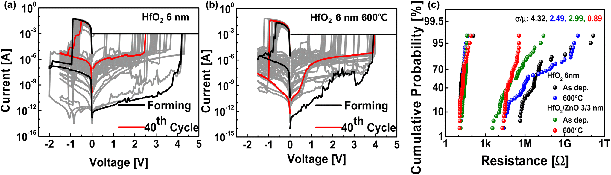 | ||
| Fig. 7 Typical I–V switching behavior of 6 nm HfO2 (a) without and with thermal annealing (b) at 600 °C for 1 h in an N2 ambient compared with that of bilayer HfO2/ZnO synaptic devices under the same thermal annealing conditions. (c) Distribution and cumulative probability of the HRS and LRS of HfO2 (6 nm) and bilayer 3 nm HfO2/3 nm ZnO synaptic devices without and with thermal annealing. | ||
3.3. Applications of artificial synapses and neurons
In the human brain, the transmission between pre-synaptic and post-synaptic neurotransmitters is substituted into the artificial synaptic device, which is comparable to the electrical switching behavior of synaptic devices.51 The repeated pre-synaptic potential firing progressively changes the strength of connections between the neurons modulating the synaptic weight. This phenomenon is known as synaptic plasticity, which plays an important cognitive function of the brain. The nonlinearity and symmetry of synaptic devices are also critical factors for application analysis. Fig. 8 shows the long-term potentiation (LTP) and long-term depression (LTD) of bilayer HfO2/ZnO synaptic devices without and with thermal annealing from 400 °C to 600 °C for 1 h in an N2 ambient. One hundred consecutive pulses, which consisted of a series of positive pulses (1.5 V, 800 μs) and a read pulse (0.25 V, 2.4 ms), was applied to bilayer synaptic devices during the LTP process. The negative pulses (−1.5 V, 800 μs) were reversed under the same condition during the LTD process. These behaviors agreed well with the results obtained for the I–V switching behavior with a DC sweep.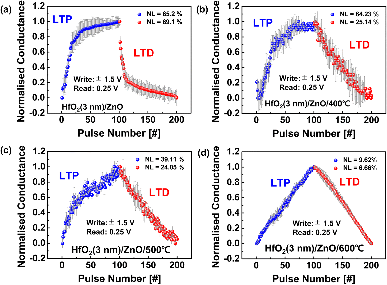 | ||
| Fig. 8 Long-term potentiation (LTP) and long-term depression (LTD) behavior of bilayer HfO2/ZnO synaptic devices (a) without and with thermal annealing at (b) 400 °C, (c) 500 °C, and (d) 600 °C for 1 h in an N2 ambient. One hundred consecutive pulses, which consisted of a series of positive pulses (1.5 V, 800 μs) and a read pulse (0.25 V, 2.4 ms), was applied to bilayer synaptic devices during the LTP process. The negative pulses (−1.5 V, 800 μs) were reversed under the same condition during the LTD process. And LTP, LTD were measured across 5 bilayer HfO2/ZnO synaptic devices, with the results presented as standard deviations. | ||
In particular, the conductance modulation of a synaptic device must be updated depending on the number of stimulation pulses between neuron spikes to achieve LTP or LTD; thus, analog switching in a biological synapse can be implemented where the weight modulation is set to various states during the adjustment of the conductance. However, most synaptic devices suffer from nonlinearity due to the mismatches of the input pulse resulting from physical limitations, including the diffusion dynamics of vacancies in resistive switching materials during the CF process. Linear conductance modulation is a major requirement for synaptic device-based neuromorphic computing to realize high accuracy for learning. The nonlinearity of synaptic devices is given by equation,30
 | (2) |
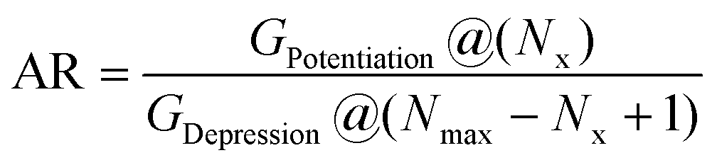
The conductance modulation of bilayer HfO2/ZnO synaptic devices without thermal annealing shows an abrupt increase, followed by gradual saturation, as shown in Fig. 8(a). The nonlinearity of the LTP and LTD characteristics is determined as 65.2% and 69.1%, respectively. The initial filament formation involves the movement of oxygen vacancies only in the vicinity of the CF. Hence, the electroforming process of bilayer HfO2/ZnO synaptic devices with thermal annealing may lead to linearity by preventing the initial abrupt increase without the filament formation process. The conductance modulation of LTP and LTP in bilayer HfO2/ZnO synaptic devices is improved by increasing the thermal annealing temperature, as shown in Fig. 8(b) and (c). The nonlinearity of LTP and LTD characteristics with thermal annealing is 64.23% and 25.14% at 400 °C, and 39.11% and 24.05% at 500 °C, respectively. In particular, the conductance modulation of bilayer HfO2/ZnO synaptic devices improves substantially with thermal annealing at 600 °C. The nonlinearity of the LTP and LTD characteristics at 600 °C was 9.62% and 6.66%, respectively. This implies that grain boundaries act as high diffusion paths for oxygen vacancies in the annealed nanocrystalline ZnO films upon the increase in grain size. Blocking the concentration of the electric field in the HfO2 layer also prevents a sudden change in conductance at the beginning as the electroforming-free process.52 To verify the device-to-device uniformity of LTP and LTD, measurements were performed on 5 bilayer HfO2/ZnO synaptic devices in each structure. Subsequently, numerical values were inserted as standard deviations, and it was observed that the HfO2/ZnO synaptic device with thermal annealing from 600 °C exhibited the least variability. The asymmetric synapse behavior during the learning process with pulse trains is important in the overall efficiency of neuromorphic computing, as well as the nonlinearity of the results. The symmetric weights of LTP and LTD in bilayer HfO2/ZnO synaptic devices are redefined as the asymmetry ratio (AR):53
 | (3) |
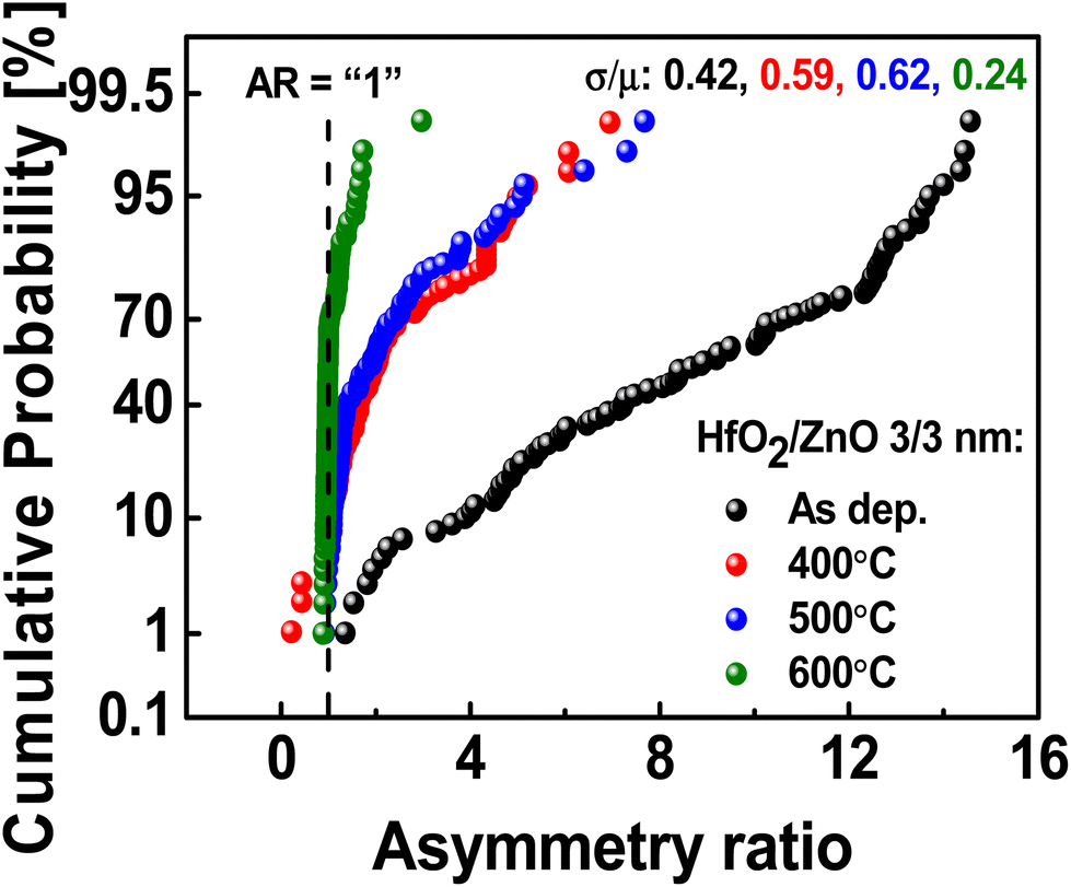
The cumulative probability of the AR for LTP and LTD in bilayer HfO2/ZnO synaptic devices without and with thermal annealing from 400 °C to 600 °C for 1 h in an N2 ambient is plotted in Fig. 9. The coefficient of variation σ/μ, where σ is the standard deviation, and μ is the mean value of the AR, gradually improves as the annealing temperature increases. An AR value closer to “1” means that data fluctuations are small. These behaviors matched well with the nonlinearity results.54 To verify the cycle-to-cycle variation of LTP and LTD, we applied a continuous pulse to HfO2/ZnO synaptic devices with thermal annealing at 600 °C. We delivered 100 positive pulses followed by 100 negative pulses and repeated this process a total of four times. For LTP, with each repetition of measurements, observed an increase in nonlinearity from 9.62% to 11.63%, 16.47%, and 19.84%. In the case of LTD, the nonlinearity increased from 6.66% to 24.23%, 7.92%, and 30.63%. This indicates that uniformity is maintained even with repeated cycles.
 | ||
| Fig. 9 Cumulative probability of the asymmetry ratio for LTP and LTD behavior in bilayer HfO2/ZnO synaptic devices without and with thermal annealing from 400 °C to 600 °C for 1 h in an N2 ambient, where the ratio “1” is the ideal state. | ||
A schematic illustration of the transition mechanism during CF formation in bilayer HfO2/ZnO synaptic devices without and with thermal annealing is shown in Fig. 11. Oxygen ions (O2−) in bilayer HfO2/ZnO synaptic devices without thermal annealing diffuse from HfO2 toward ZnO and the top electrode interface upon the applied electrical field, as shown in Fig. 10(a). Currently, oxygen vacancies are generated in the HfO2 layer and facilitate CF formation, indicating that bilayer HfO2/ZnO synaptic devices increase the conductance. The ZnO layer between the top Pd electrode and the HfO2 layer plays a significant role in electroforming-free resistive switching by easily forming oxygen deficiency in the active ZnO layer–top electrode interface. In particular, the crystallized ZnO film formed by thermal annealing between the top Pd electrode and the devices treated at 600 °C is improved.
 | ||
| Fig. 10 Conductance saturation characteristics of HfO2/ZnO synaptic devices with thermal annealing at 600 °C under a series of positive pulses with different voltage amplitude. | ||
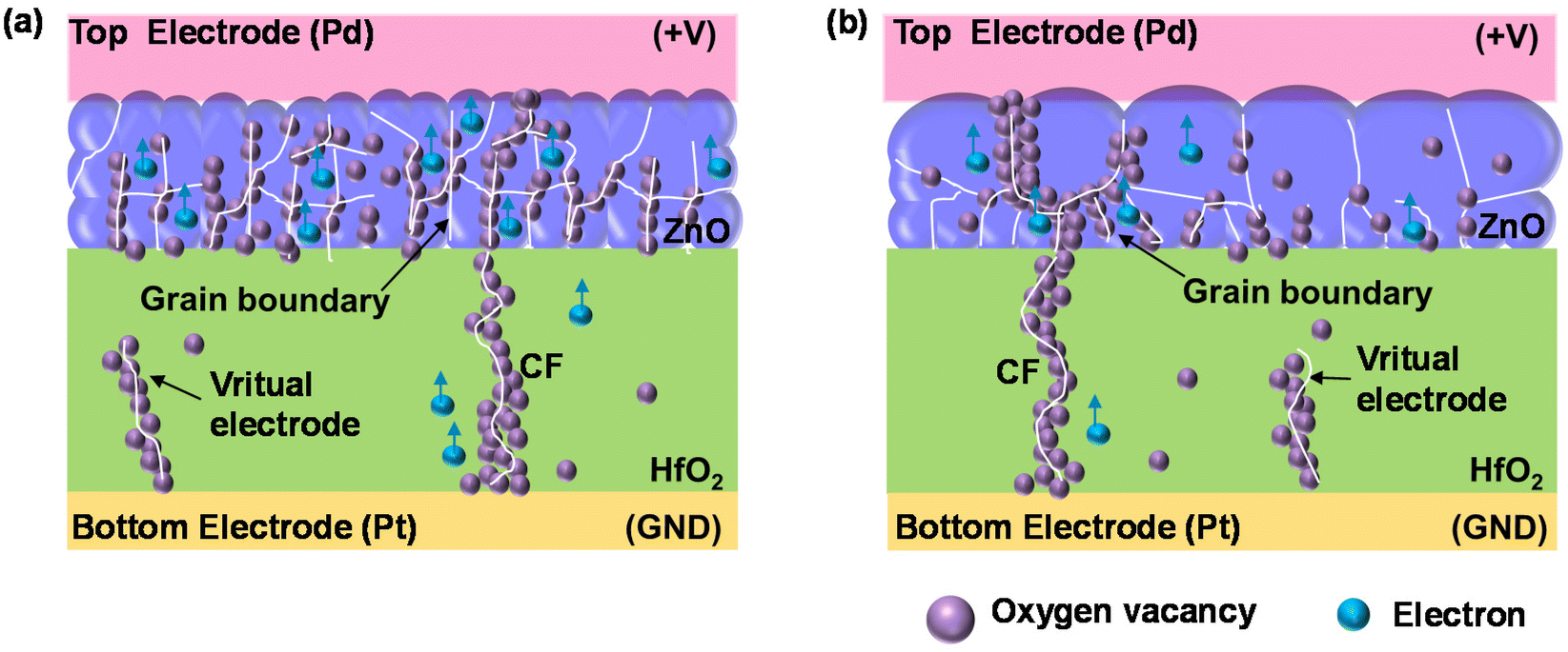 | ||
| Fig. 11 Schematic illustration of the transition mechanism during the conductive filamentary formation in bilayer HfO2/ZnO synaptic devices (a) without and (b) with thermal annealing. Crystallized ZnO films formed by thermal annealing between the top Pd electrode and the HfO2 layer remarkably improve O2− migration from the HfO2 layer to the ZnO bulk and the top electrode interface. | ||
HfO2 layer remarkably improves O2− migration from the HfO2 layer to the ZnO bulk and top electrode interface, as shown in Fig. 10(b). In other words, O2− in the HfO2 layer aggressively migrates toward the top Pd electrode and then gets trapped at the ZnO–top electrode interface or the grain boundaries of the annealed ZnO layer in addition to blocking the concentration of the electric field in the HfO2 layer. Therefore, the increased grain size in the annealed nanocrystalline ZnO films provides a robust improvement in the analog resistive switching uniformity, stability, and reliability of synaptic devices.
Also, comparing to the previous reports shown in Table 1, it is clear that the performance of the HfO2/ZnO synaptic devices treated at 600 °C is improved.
| Structure (TE/material/BE) | Switching speed | V reset/Vset | ΔR=Roff/Ron |
NL%(LTP/LTD) | Asymmetry | Ref. |
|---|---|---|---|---|---|---|
| TE, top electrode; BE, bottom electrode; RT, room temperature; NL, nonlinearity; “—”, data not found in the associated reference paper. | ||||||
| Pt/ZnO/Pt | 10 ms | −0.5 V/1 V | 102 | — | — | 55 |
| TiN/HfO2/TiN | <10 ns | −1.4 V/1.5 V | 102 | — | — | 56 |
| Pt/ZnO1−-x/ZnO bilayer structure/Pt | — | −0.6 V/1.5 V | 40 | — | — | 57 |
| Ti/ZnO/HfO2/Pt | — | — | Order of ∼102 | — | — | 58 |
| TiN/ZnO/Pt | — | −1.2 V/1.2 V | 10 | — | — | 59 |
| Pt/HfO2/ZnO/TiN | — | −1.7 V/1.4 V | 30 | — | — | 60 |
| Pd/ZnO(annealing)/HfO2/Pt | — | −0.5 V/1 V | >103 | 9.62/6.66 | ∼1 | This work |
4. Conclusions
The effects of thermal annealing on analog resistive switching behavior in bilayer HfO2/ZnO synaptic devices were investigated. The annealed active ZnO layer between the top Pd electrode and the HfO2 layer played a significant role in the resulting electroforming-free resistive switching behavior by easily forming oxygen deficiency in the ZnO layer. AFM and XRD analyses revealed that the grain size of ZnO increased as the annealing temperature increased from 400 °C to 700 °C, while the diffraction peaks of HfO2 were not found. To verify the role of the film thickness and the annealed ZnO layer in a bilayer HfO2/ZnO structure, the resistive switching behavior in single-layer HfO2 (6 nm) and bilayer HfO2/ZnO without and with thermal annealing at 600 °C was compared. We found that the analog resistive switching behavior (switching uniformity, stability, and reliability) of synaptic devices significantly improved upon thermal annealing in bilayer HfO2/ZnO synaptic devices. The switching uniformity and stability of synaptic devices demonstrated in this work are promising for the development of neural networks in the future.Author contributions
J. Jeong conceived the idea, H. M. Kwon designed the experiment, and supervised the work. Y. J. An did most of the fabricating samples and analysed the data, Yan Han did the experiment and gathered the analysis data. C. Yeom did analysed the data. S. B. Eadi assisted analyzation of the physical properties. H. D. Lee, and H. M. Kwon supervised the manuscript and developed the final manuscript.Conflicts of interest
There are no conflicts to declare.Acknowledgements
This research was supported by the Basic Science Research Program through the National Research Foundation of Korea (NRF) funded by the Ministry of Education (RS-2023-00249430). It was also funded by the Korean Government (MSIT) (Grant NRF-2022R1F1A100895). Furthermore, this research received support from the ‘Regional Innovation Strategy (RIS)’ through the National Research Foundation of Korea (NRF) funded by the Ministry of Education (MOE) (2021RIS-004).References
- B. Yan, B. Li, X. Qiao, C.-X. Xue, M. F. Chang, Y. Chen and H. Li, Adv. Intell. Syst., 2019, 1, 1900068 CrossRef.
- Q.-F. Ou, B.-S. Xiong, L. Yu, J. Wen, L. Wang and Y. Tong, Materials, 2020, 13, 3532 CrossRef CAS PubMed.
- Y. Park and J.-S. Lee, ACS Nano, 2017, 11, 8962–8969 CrossRef CAS PubMed.
- M. E. Beck, A. Shylendra, V. K. Sangwan, S. Guo, W. A. Gaviria Rojas, H. Yoo, H. Bergeron, K. Su, A. R. Trivedi and M. C. Hersam, Nat. Commun., 2020, 11, 1565 CrossRef CAS PubMed.
- M. Prezioso, F. Merrikh-Bayat, B. D. Hoskins, G. C. Adam, K. K. Likharev and D. B. Strukov, Nature, 2015, 521, 61–64 CrossRef CAS PubMed.
- M. Prezioso, M. R. Mahmoodi, F. Merrikh Bayat, H. Nili, H. Kim, A. Vincent and D. B. Strukov, Nat. Comm., 2018, 9, 5311 CrossRef CAS PubMed.
- I. Boybat, M. Le Gallo, S. Nandakumar, T. Moraitis, T. Parnell, T. Tuma, B. Rajendran, Y. Leblebici, A. Sebastian and E. Eleftheriou, Nat. Commun., 2018, 9, 2514 CrossRef PubMed.
- N. K. Upadhyay, H. Jiang, Z. Wang, S. Asapu, Q. Xia and J. Joshua Yang, Adv. Mater. Technol., 2019, 4, 1800589 CrossRef.
- S. H. Jo, T. Chang, I. Ebong, B. B. Bhadviya, P. Mazumder and W. Lu, Nano Lett., 2010, 10, 1297–1301 CrossRef CAS PubMed.
- Z. Wang, S. Joshi, S. E. Savel'ev, H. Jiang, R. Midya, P. Lin, M. Hu, N. Ge, J. P. Strachan and Z. Li, Nat. Mater., 2017, 16, 101–108 CrossRef CAS PubMed.
- L. Chua, IEEE Trans. Circuit Theory, 1971, 18, 507–519 Search PubMed.
- J. Q. Yang, R. Wang, Y. Ren, J. Y. Mao, Z. P. Wang, Y. Zhou and S. T. Han, Adv. Mater., 2020, 32, 2003610 CrossRef PubMed.
- B. Mohammad, M. A. Jaoude, V. Kumar, D. M. Al Homouz, H. A. Nahla, M. Al-Qutayri and N. Christoforou, Nanotechnol. Rev., 2016, 5, 311–329 CAS.
- Y. Zhang, G.-Q. Mao, X. Zhao, Y. Li, M. Zhang, Z. Wu, W. Wu, H. Sun, Y. Guo and L. Wang, Nat. Commun., 2021, 12, 7232 CrossRef CAS PubMed.
- M. Kumar, S. Abbas, J.-H. Lee and J. Kim, Nanoscale, 2019, 11, 15596–15604 RSC.
- E. J. Topol, Nat. Med., 2019, 25, 44–56 CrossRef CAS PubMed.
- A. S. Sokolov, H. Abbas, Y. Abbas and C. Choi, J. Semicond., 2021, 42, 013101 CrossRef.
- H. Yang, B. Chen, B. Song, D. Meng, S. Tiwari, A. Krishnamoorthy, X. Yan, Z. Liu, Y. Wang and P. Hu, ACS Appl. Electron. Mater., 2020, 2, 1529–1537 CrossRef CAS.
- R. Jiang, Z. Han and X. Du, Microelectron. Reliab., 2016, 63, 37–41 CrossRef CAS.
- P. W. Ho, F. O. Hatem, H. A. F. Almurib and T. N. Kumar, J. Semicond., 2016, 37, 064001 CrossRef.
- H. Zhai, J. Kong, J. Yang, J. Xu, Q. Xu, H. Sun, A. Li and D. Wu, J. Mater. Sci. Technol., 2016, 32, 676–680 CrossRef CAS.
- A. Khiat, S. Cortese, A. Serb and T. Prodromakis, Nanotechnology, 2016, 28, 025303 CrossRef PubMed.
- M. Ismail, H. Abbas, C. Choi and S. Kim, Appl. Surf. Sci., 2020, 529, 147107 CrossRef CAS.
- M. Azzaz, E. Vianello, B. Sklenard, P. Blaise, A. Roule, C. Sabbione, S. Bernasconi, C. Charpin, C. Cagli and E. Jalaguier, Endurance/Retention Trade Off in HfOx and TaOx Based RRAM, 2016 IEEE 8th International Memory Workshop (IMW), 2016, pp. 1–4, DOI:10.1109/IMW.2016.7495268.
- J. Kim, A. I. Inamdar, Y. Jo, H. Woo, S. Cho, S. M. Pawar, H. Kim and H. Im, ACS Appl. Mater. Interfaces, 2016, 8, 9499–9505 CrossRef CAS PubMed.
- X.-D. Huang, Y. Li, H.-Y. Li and X.-S. Miao, Low-power, High Speed and High Uniform Switching in AIOx-based Memristor using Homogeneous Bilayer Structure for Memcomputing, 2019 IEEE International Conference on Integrated Circuits, Technologies and Applications (ICTA), 2019, pp. 113–114, DOI:10.1109/ICTA48799.2019.9012899.
- G. Niu, M. Schubert, S. Sharath, P. Zaumseil, S. Vogel, C. Wenger, E. Hildebrandt, S. Bhupathi, E. Perez and L. Alff, Nanotechnology, 2017, 28, 215702 CrossRef CAS PubMed.
- X. Chen, N. Wu and A. Ignatiev, Perovskite RRAM devices with metal/insulator/PCMO/metal heterostructures, Symposium Non-Volatile Memory Technology, 2005, pp. 4–128, DOI:10.1109/NVMT.2005.1541418.
- G. S. Kim, H. Song, Y. K. Lee, J. H. Kim, W. Kim, T. H. Park, H. J. Kim, K. Min Kim and C. S. Hwang, ACS Appl. Mater. Interfaces, 2019, 11, 47063–47072 CrossRef CAS PubMed.
- H.-W. Choi, K.-W. Song, S.-H. Kim, K. T. Nguyen, S. B. Eadi, H.-M. Kwon and H.-D. Lee, Sci. Rep., 2022, 12, 1259 CrossRef CAS PubMed.
- Z. Q. Wang, H. Y. Xu, X. H. Li, H. Yu, Y. C. Liu and X. J. Zhu, Adv. Funct. Mater., 2012, 22, 2759–2765 CrossRef CAS.
- J. J. Yang, M. D. Pickett, X. Li, D. A. Ohlberg, D. R. Stewart and R. S. Williams, Nat. Nanotechnol., 2008, 3, 429–433 CrossRef CAS PubMed.
- K. Wang, Y. Chang, L. Lv and Y. Long, Appl. Surf. Sci., 2015, 351, 164–168 CrossRef CAS.
- G. Yao, Z. Qu, C. Li, Y. Peng, Q. Li, Z. Zeng, J. Dong and B. Zhang, J. Nanomater., 2022, 911, 165105 Search PubMed.
- K.-H. Son and H.-S. Lee, Appl. Surf. Sci., 2022, 575, 151754 CrossRef CAS.
- A. Tschöpe, C. Bäuerle and R. Birringer, J. Appl. Phys., 2004, 95, 1203–1210 CrossRef.
- A. Kaźmierczak-Bałata, L. Grządziel, M. Guziewicz, V. Venkatachalapathy, A. Kuznetsov and M. Krzywiecki, Appl. Surf. Sci., 2021, 546, 149095 CrossRef.
- G. S. Rohrer, J. Am. Ceram. Soc., 2011, 94, 633–646 CrossRef CAS.
- Y. Li and K.-W. Ang, Adv. Intell. Syst., 2021, 3, 2000137 CrossRef.
- A. Bietsch and B. Michel, Appl. Phys. Lett., 2002, 80, 3346–3348 CrossRef CAS.
- K. Awsiuk, A. Bernasik, M. Kitsara, A. Budkowski, J. Rysz, J. Haberko, P. Petrou, K. Beltsios and J. Raczkowska, Colloids Surf., B, 2010, 80, 63–71 CrossRef CAS PubMed.
- J. E. Kim, J. U. Kwon, S. Y. Chun, Y. G. Song, D. S. Jeong, C. Y. Kang, S. K. Kim, S. Nahm and J. H. Yoon, Adv. Electron. Mater., 2022, 8, 2200365 CrossRef CAS.
- F. Acosta-Humánez, O. Almanza and C. Vargas-Hernández, Superficies Vacio, 2014, 27, 43–48 Search PubMed.
- H. Dhasmana, S. Shital and V. Dutta, J. Mater. Sci.: Mater. Electron., 2014, 25, 4095–4102 CrossRef CAS.
- N. Fujimura, T. Nishihara, S. Goto, J. Xu and T. Ito, J. Cryst. Growth, 1993, 130, 269–279 CrossRef CAS.
- A. I. A. Rani, G. B. Kumar, K. A. Mohamad, M. S. Osman, F. P. Chee and I. Saad, J. Phys.: Conf. Ser., 2019, 1358, 012045 CrossRef.
- S. Munjal and N. Khare, Appl. Phys. Lett., 2018, 112, 073502 CrossRef.
- R. Yang, K. Terabe, Y. Yao, T. Tsuruoka, T. Hasegawa, J. K. Gimzewski and M. Aono, Nanotechnology, 2013, 24, 384003 CrossRef PubMed.
- C.-C. Hsu, P.-T. Liu, K.-J. Gan, D.-B. Ruan and S. M. Sze, Vacuum, 2022, 201, 111123 CrossRef CAS.
- U. Chand, C.-Y. Huang and T.-Y. Tseng, IEEE Electron Device Lett., 2014, 35, 1019–1021 CAS.
- Z. Shen, C. Zhao, Y. Qi, W. Xu, Y. Liu, I. Z. Mitrovic, L. Yang and C. Zhao, Nanomaterials, 2020, 10, 1437 CrossRef CAS PubMed.
- J. H. Yoon, J. Zhang, X. Ren, Z. Wang, H. Wu, Z. Li, M. Barnell, Q. Wu, L. J. Lauhon and Q. Xia, Adv. Funct. Mater., 2017, 27, 1702010 CrossRef.
- C. Lee, S.-M. Koo, J.-M. Oh and D. Lee, IEEE J. Electron Devices Soc., 2018, 6, 403–407 CAS.
- Y. J. An, B. Bathula, K. Yoo, H. M. Kwon, S. B. Eadi and H. D. Lee, Mater. Lett., 2023, 341, 134193 CrossRef CAS.
- F.-C. Chiu, Adv. Mater. Sci. Eng., 2013, 2013, 362053 Search PubMed.
- H. Kim, P. C. McIntyre, C. O. Chui, K. C. Saraswat and S. Stemmer, J. Appl. Phys., 2004, 96, 3467–3472 CrossRef CAS.
- C. H. Huang, J. S. Huang, S. M. Lin, W. Y. Chang, J. H. He and Y. L. Chueh, ACS Nano, 2012, 6, 8407–8414 CrossRef CAS PubMed.
- N. Jain, S. K. Sharma, R. Kumawat, P. K. Jain, D. Kumar and R. Vyas, Micro Nanostruct., 2022, 169, 207366 CrossRef CAS.
- N. Xu, L. Liu, X. Sun, C. Chen, Y. Wang, D. Han, X. Liu, R. Han, J. Kang and B. Yu, Semicond. Sci. Technol., 2008, 23, 075019 CrossRef.
- C. Liu, L. Zhu, L.-G. Wang and A.-D. Li, in Memristor-An Emerging Device for Post-Moore's Computing and Applications, IntechOpen, 2021 Search PubMed.
Footnotes |
| † Electronic supplementary information (ESI) available. See DOI: https://doi.org/10.1039/d3nr04917e |
| ‡ These authors contribute equally to this work. |
| This journal is © The Royal Society of Chemistry 2024 |