DOI:
10.1039/D4NH00072B
(Communication)
Nanoscale Horiz., 2024,
9, 775-784
Analytical modelling of the transport in analog filamentary conductive-metal-oxide/HfOx ReRAM devices†
Received
16th February 2024
, Accepted 19th March 2024
First published on 22nd March 2024
Abstract
The recent co-optimization of memristive technologies and programming algorithms enabled neural networks training with in-memory computing systems. In this context, novel analog filamentary conductive-metal-oxide (CMO)/HfOx redox-based resistive switching memory (ReRAM) represents a key technology. Despite device performance enhancements reported in literature, the underlying mechanism behind resistive switching is not fully understood. This work presents the first physics-based analytical model of the current transport and of the resistive switching in these devices. As a case study, analog TaOx/HfOx ReRAM devices are considered. The current transport is explained by a trap-to-trap tunneling process, and the resistive switching by a modulation of the defect density within the sub-band of the TaOx that behaves as electric field and temperature confinement layer. The local temperature and electric field distributions are derived from the solution of the electric and heat transport equations in a 3D finite element ReRAM model. The intermediate resistive states are described as a gradual modulation of the TaOx defect density, which results in a variation of its electrical conductivity. The drift-dynamics of ions during the resistive switching is analytically described, allowing the estimation of defect migration energies in the TaOx layer. Moreover, the role of the electro-thermal properties of the CMO layer is unveiled. The proposed analytical model accurately describes the experimental switching characteristic of analog TaOx/HfOx ReRAM devices, increasing the physical understanding and providing the equations necessary for circuit simulations incorporating this technology.
New concepts
Advancements in both technology and training algorithms are required to enable analog in-memory hardware execution of neural network training workloads. Due to the bidirectional accumulative analog response, conductive-metal-oxide (CMO)/HfOx ReRAM devices may represent a technological breakthrough in this context. This work presents the first physics-based analytical model of the current transport and of the resistive switching in the CMO/HfOx ReRAM technology. The experimental switching characteristic of these devices is described by a trap-to-trap tunnelling process according to the Mott and Gurney analytically formulation. The resistive switching is dominated by the defect dynamics in the CMO layer rather than in the conductive filament as per conventional metal/HfOx/metal ReRAM technology. Compared to such conventional ReRAM technology, the bidirectional accumulative analog response of the CMO/HfOx ReRAM devices is attributed to the change from a full defect depletion/accumulation of a tiny gap in the conductive filament to a partial defect modulation in a larger half spherical CMO volume. Furthermore, the CMO is unveiled to act as both a thermal and electric field confinement layer in the CMO/HfOx ReRAM devices. This study sets the groundwork for further CMO/HfOx ReRAM technology optimization and provides the transport equations necessary for circuit simulations incorporating this technology.
|
Introduction
Analog AI inference and training
The recurrent data transfer between memory and processing units is a key source of speed and energy inefficiency in the hardware implementation of artificial neural networks (ANNs).1 To address this challenge, modern digital AI accelerators enhance computational parallelism and bring memory closer to the processing units.2 However, due to the limited on-chip memory capacity and the increasing number of parameters in modern ANNs, communication with off-chip memory is still needed.3,4 To overcome this memory wall, a promising approach, known as analog in-memory computing (AIMC),5 consists of transitioning to a hybrid architecture where some of the arithmetic and logic operations can be performed at the location where the data is stored.6 Emerging resistive memory (memristive) technologies such as redox-based resistive switching memory (ReRAM),7 phase-change memory (PCM)8 and magnetoresistive random access memory (MRAM),9 are particularly well suited for the AIMC computing paradigm.10 By organizing memristive devices in a crossbar configuration, matrix-vector multiplications (MVMs) can be performed directly in-memory by exploiting the multi-level storage capability of the devices, combined with Ohms law and Kirchhoffs law, in O(1) time complexity.11,12 AIMC-based AI hardware accelerator exploration has been mainly confined to inference workloads,13 being the accuracy of conventional training algorithms, such as the stochastic gradient descent (SGD), strongly dependent on the switching characteristics of the memristive devices.14 In particular, the key device requirement is the linear and symmetric conductance update in response to positive or negative pulse stimuli. However, since memristive devices exhibit non-ideal characteristics,15,16 advancements in both technology and training algorithms are required to achieve a full AIMC training system for deep learning workloads. Recent studies have demonstrated that parallel updates of AIMC ReRAM-based architecture may achieve a significant improvement in both energy efficiency and speed during neural network training with respect to digital AI accelerators.17,18 To address this challenge, a new ANN training algorithm, known as Tiki-Taka,14 was recently developed and optimized for analog resistive device. The core advantage of Tiki-Taka is to limit the device symmetry requirements from the entire conductance (G) window to a local symmetry point, where the changes in G are equal in both upward and downward directions.14 The key device requirement for the Tiki-Taka algorithm is analog resistive switching in both directions using a stream of identical pulses. To achieve so, the introduction of a properly engineered conductive-metal-oxide (CMO) in the conventional HfOx-based ReRAM metal/insulator/metal (M/I/M) stack has been shown to lead to crucial device optimization.19 Such M/CMO/I/M ReRAM devices exhibit improved characteristics in terms of analog states, stochasticity, symmetry point and endurance, compared to conventional M/I/M technology,18 paving the way for AIMC training units using ReRAM crossbar arrays.
Origin of resistive switching
The origin of the resistive switching process in filamentary M/I/M HfOx-based ReRAM device is commonly attributed to the migration of oxygen vacancies in an oxygen-deficient conductive filament (CF).20 Such migration results in a purely filamentary conduction in the low resistance state (LRS) and tunneling transport through a low oxygen vacancy concentration region, known as gap, in the high resistance state (HRS).20 In contrast, the underlying mechanism behind the resistive switching in analog M/CMO/I/M HfOx-based ReRAM device is not fully understood, despite its device performance improvements. A recent study21 focuses on the electro-thermal modelling of static current transport in both LRS and HRS within a similar M/CMO/I/M ReRAM structure. However, the analytical current transport description and the switching dynamics, both crucial for a compact model description and consequently circuit simulations, remain unknown.22,23
Analog CMO/HfOx ReRAM devices
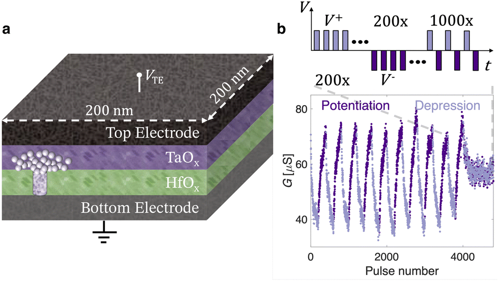
This work addresses this challenge by providing a physics-based analytical model of the conduction in analog M/CMO/I/M HfOx-based ReRAM devices. The electron transport and the drift ion dynamics are both analytically described in LRS, HRS, intermediate analog states and during the SET (from HRS to LRS) and RESET (from LRS to HRS) transitions. The model results are compared to experimental data measured on a representative TiN/TaOx/HfOx/TiN ReRAM device, with a cell area of (200 nm)2 and the same stack as reported in our previous work.24Fig. 1a shows a simplified cross-sectional schematic of the analog TaOx/HfOx ReRAM devices, in shared bottom electrode configuration, modelled in this work. The bidirectional accumulative ReRAM response under the application of trains of identical voltage pulses with alternating polarity in batches of 200, is illustrated in Fig. 1b. This pulse scheme is repeated 10 times, showing a stable G window. Finally, by alternately applying a single up pulse and down pulse, a stable G symmetry point is achieved. This process replicates the programming conditions utilized in Tiki-Taka training.14 As reported in our previous works,25,26 analog TaOx/HfOx ReRAM devices are characterized by ISET ≈ IRESET and consequently VSET ≈ VRESET. However, to increase the switching ratio (RHRS/RLRS), a larger stop voltage amplitude is desirable for the RESET compared to the SET process (|Vstop,RESET| > |Vstop,SET|). The fabrication process is detailed in our previous work,24 while additional information on the electrical characterization of ReRAM is reported in the Methods section of the ESI.† Although in Tiki-Taka training applications the targeted programming scheme employs short pulses (from hundreds of ps27 to μs24), quasi-static current–voltage (I–V) characterization of the ReRAM device is required to model the physics of the steady-state current transport. However, by cycling the TaOx/HfOx devices with quasi-static voltage excitations, intentionally without current compliance control to prevent masking device physics during the switching, the conductance window shifts toward larger G values by a factor of around 3, as shown in Fig. 2b and d. Nevertheless, the physics-based analytical current transport model developed in this work and applied to such TaOx/HfOx devices, can also be used to explain other similar analog M/CMO/I/M ReRAM systems, including those with lower average conductance.
 |
| | Fig. 1 (a) Schematic illustration of the ReRAM device cross-section profile. (b) Bidirectional accumulative analog ReRAM response and symmetry point. The applied pulses have identical amplitudes of +1.6 V for the downward direction (G depression) and −1.4 V for the upward direction (G potentiation), each with a constant duration of 600 ns. After each pulse, the devices resistance is measured by 10 μs read pulses of ±0.2 V. The top inset shows the electrical testing scheme utilized to evaluate the analog switching properties of the ReRAM device for the Tiki-Taka algorithm. | |
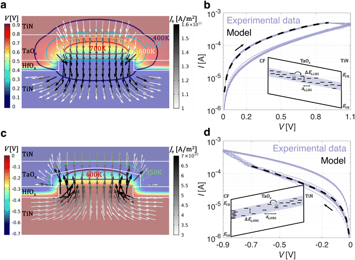 |
| | Fig. 2 The steady-state 2D spatial distributions of T, V and Je in a TaOx/HfOx ReRAM device is shown (a) in LRS with a constant bias of 0.9 V and (c) in HRS with a constant bias of −0.7 V. Both T and V are locally confined in a 3D half-spherical volume in the TaOx layer. The key purpose of the CF is the Je confinement. The electro-thermal energy confinement in the TaOx layer leads to the (a) RESET or (c) SET switching process. The experimental quasi-static I–V characteristic of a TaOx/HfOx ReRAM device and the analytical electron trap-to-trap tunneling model are reported (b) in LRS and (d) HRS. The bottom insets in (b) and (d) show a schematic sketch of the trap-to-trap tunneling transport in the TaOx sub-band, considering the CF and the TiN as electrodes, in LRS and HRS respectively. | |
Physics-based analytical model
Current transport: the model
In sub-stoichiometric metal-oxides, a significant concentration of defects related to oxygen vacancies and metal interstitials is observed.28–30 Each defect forms isolated donor-like states in the band gap of the metal-oxide, which become a sub-band for large defect concentrations.28,31–33 In oxides with a high band gap, there can be a substantial energetic separation (activation energy) between the defect states and the lower edge of the conduction band ECB. For example, in TaOx, the spectral location of the defect state sub-band associated with oxygen vacancies has been reported to be in the midgap, approximately 2 eV above the top of the valence band EVB.32 Consequently, according to the energy band alignment between the Fermi level of the electrodes and the defect sub-band in the conductive metal-oxide, it is likely that electrons coming from one electrode are trapped in the defect states during the current transport. However, to actively contribute to the conduction, trapped electrons must be released. Depending on the defect activation energy in the conductive metal-oxide, two scenarios may occur: the electrons get released by thermal excitation in the conduction band, or they tunnel from trap-to-trap until reaching the other electrode. In this work, due to midgap electronic states in the TaOx layer, the electronic current Ie in a filamentary HfOx/TaOx ReRAM device is modelled as a trap-to-trap tunneling process in the TaOx layer, based on the description provided by Mott and Gurney.34 It describes electron-hopping conduction over an energy barrier ΔEe, which is identical in every direction in the absence of an electric field. Application of an electric field modifies the energy barrier by ∓eaeE/2 for forward (backward) jumps, resulting in a lowered (raised) barrier.| |  | (1) |
In eqn (1), e is the elementary charge, kB is the Boltzmanns constant, ae is the hopping distance, ν0,e is the electron attempt frequency, Ne is the density of electronic defect states in the TaOx band gap, ΔEe is the zero-field hopping energy barrier, T and E are the local temperature and electric field, respectively, and A = πrCF2, rCF being the filament radius, is the cross-sectional area of the filament at the interface with the TaOx layer. Among the different types of defects in the TaOx layer, this work focuses on oxygen vacancy defects  , which have been reported to generally have lower formation and migration energies with respect to Tai interstitials.29,30 Each double-positively charged vacancy
  generates two electronic defect states in the band gap.30 Therefore, the maximum density of defect states Nmaxe that may contribute to the transport can be related to the ionic vacancy concentration
  , according to
  . Depending on the energy alignment between the defect sub-band in the TaOx layer and the Fermi level of the electrodes, statistically only a sub-set of the defect states Ne contributes to the electronic transport, resulting in eqn (2).
| |  | (2) |
where
β is a scaling factor between 0 and 1 to filter out the defect states that are not contributing to the conduction.
Defect drift dynamics: the model
In addition to electronic transport, the description of the ion dynamics is crucial for understanding the resistive switching process and the resulting structural material changes. To do so, the drift dynamics of the ionic defects  in the TaOx layer during the SET and RESET processes is similarly described by an ion-hopping conduction over a migration energy barrier ΔEion,35 according to eqn (3) and (4),
| |  | (3) |
| |  | (4) |
where vMott–Gurneyion,drift is the ion drift velocity,  is the charge number of the oxygen vacancies relative to the perfect crystal, aion is the crystal hopping distance and ν0,ion is the ion attempt frequency.
3D finite element model (FEM)
The local temperature T and electric field E distributions in the steady state of TaOx/HfOx ReRAM devices are assessed using a space resolved 3D FEM developed with COMSOL Multiphysics 5.2 software, according to eqn (5) and (6).where Je is the electric current density, σ the electrical conductivity, V the electric potential, k the thermal conductivity and Qe the heat source due to Joule heating. Table 1 lists the basic simulations parameters used in this work, taken from literature.
Table 1 Simulation parameters from literature
| Symbol |
Value |
Symbol |
Value |
|
ν
0,ion
|
4 × 10¹² Hz![[thin space (1/6-em)]](https://www.rsc.org/images/entities/char_2009.gif) 35 35 |
ν
0,e
|
2 × 10¹³ Hz36 |
|
a
ion
|
0.4 nm 37 |
k
TaOx
|
1 W (m K)−138 |
|
k
HfOx
|
0.5 W (m K)−139 |
k
CF
|
23 W (m K)−140 |
|
k
TiN,Sputter
|
3 W (m K)−141 |
k
TiN,ALD
|
11 W (m K)−142 |
|
σ
HfOx
|
1 × 10⁻⁴ Sm−1 |
σ
CF
|
4.2 × 10⁴ S m−121 |
|
σ
TiN
|
5 × 10⁵ S m−143 |
Sweep rate |
0.1 V s−1 |
|
T
0
|
293 K |

|
2 |
The boundary conditions include the current conservation to all the domains, and electric isolation (n·Je = 0), where n is the outward normal vector, to all the vertical external boundaries such that no electric current flows through the boundaries. The electric potential is always applied to the ReRAM device top electrode, with the bottom electrode serving as the ground node, as shown in Fig. 1a. In the 3D FEM, all external boundaries of the ReRAM device are maintained at room temperature T0 in steady state, as negligible heating is expected far from the switching area. The model takes into account the entire experimental TaOx/HfOx ReRAM device area of (200 nm)2.
Results and discussion
Analytical model of the LRS and HRS
An high-resolution scanning transmission electron microscopy (STEM) measurement on a similar TaOx/HfOx ReRAM stack unveils a thin oxygen-rich TaOx amorphous phase (≈3 nm) between the crystalline oxygen-deficient TaOx and the HfOx layer.25,26 The amorphous TaOx phase, combined with the reduced oxygen scavenging capabilities of TaOx material with respect to Ti,44,45 results in an increase of the forming voltage Vforming in the TaOx/HfOx ReRAM device (≈3.6 V)24 compared to Ti/HfOx technology (≈2.5 V).26 During the forming, a dielectric breakdown occurs in the HfOx and oxygen-rich amorphous TaOx layers, leading to the formation of a highly defect-rich conductive filament in both layers.25 For oxygen vacancy defects, reported formation energies range from 2.8 eV to 4.6 eV in HfOx, depending on the stoichiometry,46,47 and from 4.3 eV to 5.7 eV in TaOx, depending on the oxygen vacancy charge number.48,49 Due to the high formation energy, defect generation, both in HfOx and TaOx materials, occurs with statistical relevance only during the forming, when a large electric field and high temperature are locally reached. Therefore, the resistive switching process in a TaOx/HfOx ReRAM device is determined by the migration of pre-existing defects, which leads to the modulation of the density of defect states in the band gap of the TaOx layer. A 3D FEM is developed to simulate the electronic transport in a filamentary TaOx/HfOx ReRAM device in both LRS and HRS. The electrical conductivity of the crystalline sputtered TaOx layer is measured experimentally.26 However, due to the defect generation during the forming event, the local conductivity of the TaOx layer on top of the conductive filament will be higher. For this reason, the electrical conductivity of the crystalline TaOx layer was considered as a parameter in the 3D ReRAM model, within experimentally reported boundaries.26 From the model of the electronic conduction of the TaOx/HfOx ReRAM device in the low-voltage linear regime in LRS, both the filament radius rCF and the local conductivity of the TaOx layer σTaOx are extracted and reported in Table 2. Fig. 2a shows the steady-state 2D spatial distributions of temperature, electric potential, and current density in a TaOx/HfOx ReRAM device in LRS with a constant bias of 0.9 V, taking into account the experimental I–V non-linearity with the same approach as reported in our previous work.21 The TaOx layer, with its lower thermal conductivity (see Table 1), represents a larger thermal resistance compared to the conductive filament. For this reason, in steady state, a spatial temperature gradient exists within the TaOx layer (see Fig. 2a), acting as a thermal confinement layer,22 confining heat on top of the conductive filament. In addition, due to the combination of the filamentary current constriction and the electrical conductivity of the TaOx layer, the resistance in the LRS is dominated by the spreading resistance (Rspreading ∝ (2πσTaOxrCF)−1 ≫ RCF) between the CF and the TaOx, which leads to a nonuniform current density in the TaOx layer.21 As a consequence, by properly designing its electrical conductivity,21 the TaOx layer can also act as a field confinement layer, confining the applied electric field above the conductive filament in a half-spherical shape, as illustrated in Fig. 2a. Although the thermal and electric field confinement can similarly be achieved with an insulating metal-oxide layer, to avoid an increase of the overall forming voltage, a conductive TaOx is used. The average temperature and electric field over such a 3D half-spherical volume in the TaOx layer are calculated (see Fig. S1, ESI†), and used in eqn (1) to describe the static electronic conduction in LRS. Fig. 2b shows the experimental clockwise I–V quasi-static characteristic of a representative TaOx/HfOx ReRAM device in LRS over 10 cycles. The analytical electron trap-to-trap tunneling model in the TaOx layer (see Fig. 2b) accurately describes the experimental curve in LRS, enabling the extraction of ae,LRS, ΔEe,LRS, and Ne,LRS, as reported in Table 2. Oxygen vacancy migration in the TaOx layer has been reported as a process with an activation energy of ≈1.5 eV.30,37 As the applied positive electric potential on the TaOx/HfOx ReRAM device increases, the electro-thermal energy in the TaOx layer rises, through the local confinement of both the electric field and temperature. When the oxygen vacancy migration energy in the TaOx layer is reached, the RESET switching process starts. During the RESET process, oxygen vacancies in the TaOx layer radially migrate toward the conductive filament. Depending on the energy barrier at the TaOx/HfOx interface, two scenarios may occur: an exchange of oxygen ions between the two layers, or an accumulation of oxygen vacancies within the TaOx layer at the interface with the conductive filament.50 Both scenarios lead to a high resistance state (HRS) in the TaOx/HfOx ReRAM device, characterized by a partial defect depletion of a half-spherical volume, also referred to as a dome,21 in the TaOx layer. In this work, although it's not a binding assumption for the validity of the model, the resistive change of the TaOx/HfOx ReRAM device is primarily attributed to oxygen vacancy migration within the TaOx layer. In agreement with this interpretation, a 3D TaOx,Dome volume (VTaOx,Dome), characterized by a lower density of defect states and therefore lower electrical conductivity σTaOx,Dome (see Table 2), has been employed to model electronic conduction in TaOx/HfOx ReRAM devices in HRS. Fig. 2c shows the steady-state 2D spatial distributions of temperature, electric potential, and current density in a TaOx/HfOx ReRAM device in HRS with a constant bias of −0.7 V, taking into account the experimental I–V non-linearity with the same approach as reported in our previous work.21 Similar to the LRS, TaOx acts as both a thermal and field confinement layer (see Fig. 2c). The average temperature and electric field (see Fig. S1, ESI†) serve as inputs in eqn (1) to model the static current transport in HRS. The same analytical trap-to-trap tunneling model accurately describes the experimental curve of a TaOx/HfOx ReRAM device also in HRS (see Fig. 2d). The physical parameters characterizing the trap-to-trap tunneling process in the TaOx,Dome, ae,HRS, ΔEe,HRS, and Ne,HRS are reported in Table 2. Compared to the LRS, the less-defective TaOx,Dome volume is characterized by both a larger hopping distance ae and energy barrier ΔEe, and a lower density of defect states Ne in the band gap. By increasing the applied negative electric potential, when the required activation energy is reached, the SET switching process starts. Oxygen vacancies accumulated in the TaOx layer at the interface with the conductive filament, radially migrate back and repopulate the half-spherical TaOx,Dome, resulting in the LRS of the TaOx/HfOx ReRAM device.
Table 2 Simulation results from our model
| Symbol |
Value |
Symbol |
Value |
|
r
CF
|
25 nm |
V
TaOx,Dome
|
3 × 10⁻²³ m3 |
|
σ
TaOx
|
2 × 10³ Sm−1 |
σ
TaOx,Dome
|
0.38 × 10³ Sm−1 |
|
a
e,LRS
|
0.75 nm |
a
e,HRS
|
1.1 nm |
| ΔEe,LRS |
55 meV |
ΔEe,HRS |
88 meV |
|
N
e,LRS
|
3.6 × 1026 m−3 |
N
e,HRS
|
1.7 × 1026 m−3 |
Intermediate resistive states
By applying bipolar short pulse streams, the conductance of TaOx/HfOx ReRAM devices can be gradually potentiated or depressed, as shown in Fig. 1b. The number of states and the overall analog switching performance have been shown to improve upon the application of ultrafast pulses (down to 300 ps).27 Additionally, in our previous work,24 it was demonstrated that TaOx/HfOx ReRAM devices preserve analog properties after more than 107 programming pulses, and show stable intermediate resistive states (<4% drift after 72 h at 85 °C). Due to the excellent endurance and retention properties of TaOx/HfOx ReRAM devices, in first approximation, device non-idealities are not included in this work. The 3D FEM of the TaOx/HfOx ReRAM device was used to model the intermediate resistive states resulting from the application of quasi-static excitations with increasing amplitudes. Fig. 3a shows the experimental response of a representative TaOx/HfOx ReRAM device to quasi-static voltage sweeps with an increasing stop voltage amplitude Vstop. Even with quasi-static excitations, intermediate resistive states can be accessed during both the SET and the RESET, without any external compliance current control. Fig. 3b and c illustrate a multistate exponential relationship between the experimental resistance measured at 0.2 V and Vstop during the SET and RESET processes, respectively. A comparable trend during the RESET of a filamentary ReRAM device has already been reported,36 but not for the SET process, which is typically a self-accelerated abrupt process.20 In agreement with the interpretation provided in this work (see Fig. 2), the equivalent electrical conductivity σTaOx,Dome, assumed of a constant volume VTaOx,Dome, to model the electronic conduction in the low-voltage linear regime (see Fig. S2, ESI†), is extracted. Fig. 3b and c show the exponential evolution of the σTaOx,Dome as a function of Vstop during the SET and RESET processes, respectively.
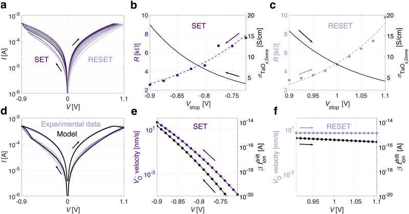 |
| | Fig. 3 (a) Experimental quasi-static voltage sweeps, where the absolute stop voltage amplitude for both SET (from −0.725 V to −0.9 V) and RESET (from 0.9 V to 1.1 V) processes increases gradually with a step of 0.25 V. The exponential stop voltage-dependent evolution of the experimental intermediate resistive states measured at 0.2 V and the simulated equivalent electrical conductivity σTaOx,Dome are reported for SET (b) and RESET (c). (d) The analytical trap-to-trap tunneling model accurately describes the experimental switching characteristic of a TaOx/HfOx ReRAM device. (e) Oxygen vacancy drift velocity and the resulting ionic current scaled by the β factor, are reported as a function of the applied quasi-static voltage for SET (e) and RESET (f), respectively. | |
Analytical model of the switching characteristic
To model the current during the entire switching characteristic, in addition to the LRS and HRS (see Fig. 2), the transport during the SET and RESET transitions has to be addressed. To do so, the analytical trends of the electro-thermal conditions and trap-to-trap tunneling parameters during such transitions, are required. In Fig. 3b and c, both resistance, based on experimental evidence, and σTaOx,Dome, based on model evidence, exhibit an exponential dependence on Vstop in the TaOx/HfOx ReRAM devices. Additionally, the electro-thermal conditions (see Fig. S1, ESI†) and trap-to-trap tunneling parameters (see ae, ΔEe and Ne from Table 2) are known at the onset of both the SET and RESET processes from the modelling of the static electronic transport. By combining these evidences, an exponential distribution for T, E, ae, ΔEe, and Ne within the static boundaries (from Fig. 2 and Table 2) is assumed to model the electronic current during both the SET and RESET transitions. Fig. 3d shows the resulting electron trap-to-trap tunneling transport model during the SET and RESET transitions according to eqn (1). The model in Fig. 3d accurately describes the experimental quasi-static switching characteristic, validating the previous assumption. During the RESET transition, the temperature slightly decreases while the electric field in the TaOx layer increases (see Fig. S3, ESI†). The simulation aligns with the interpretation presented in this work, indicating an overall increase in resistance, resulting in reduced Joule heating and a progressively increasing electric field confined within the less-defective TaOx,Dome. During the SET transition, although the applied voltage increases, the electric field in the TaOx layer stays nearly the same, while the temperature increases exponentially (see Fig. S3, ESI†). This aligns with a decrease in resistance, resulting in enhanced Joule heating and a defect-enrichment of the TaOx,Dome, restoring the LRS condition.
 drift dynamics
To explain the dynamics of the resistive switching in TaOx/HfOx ReRAM devices, the drift of  during the SET and RESET transitions is modelled. For each voltage step (10 mV) during the SET and RESET processes, the average oxygen vacancy drift velocity is computed according to eqn (3). By scaling the drift velocity with the experimental measurement time (100 ms per step), an average drift induced displacement is computed for each voltage step. The cumulative sum of the displacements during both the SET and RESET transitions, results in the average size of the dome along the vertical direction. For consistency with the current transport model (see Fig. 2), an overall oxygen vacancy displacement of approximately 10 nm is assumed for both the SET and RESET, while the ion-hopping energy barriers ΔEion,SET and ΔEion,RESET are considered as fitting parameters. The extracted ion activation energies are ΔEion,RESET = 1.44 eV and ΔEion,SET = 1.32 eV. Consistently, both energies closely align with the reported oxygen vacancy migration energy of ≈1.5 eV30 in the TaOx layer. The difference between ΔEion,RESET and ΔEion,SET may suggest that the two migrations happen through different energy paths. Oxygen vacancy accumulation at the interface with the conductive filament (during RESET) may require more energy than redistribution back into the 3D half-spherical volume (during SET). Fig. 3e and f show the oxygen vacancy drift velocity and the resulting ionic current scaled by the β factor, according to eqn (4), during the quasi-static SET and RESET, respectively. Although the β factor, which describes the sub-set of defect states contributing to conduction, may vary during the switching process, the change in βIdriftion is primarily attributed to a change in Idriftion, which depends on the electro-thermal conditions according to eqn (4). In agreement with the experimental switching characteristic, the ionic drift dynamics follow an exponentially increasing trend during SET (see Fig. 3e) and a nearly uniform one during RESET (see Fig. 3f). Future work will focus on establishing the analytical link between the
  average drift velocity and the ionic vacancy concentration
  , which determines the electronic current according to eqn (1) and (2). Although not included in this work, the competing ionic diffusion and the reaching of a saturation of the oxygen vacancy concentration in the TaOx layer, are expected to mitigate and eventually stop the drift dynamics. Compared to conventional Ti/HfOx ReRAM technology, the proposed model of a TaOx/HfOx ReRAM device shows a similar intrinsically gradual RESET, but a fundamentally different SET, from abrupt to exponential. The graduality of the SET process is explained by a new physical interpretation, from a full defect depletion/accumulation of a tiny gap in the HfOx filament to a partial modulation of defects in a larger 3D half-spherical shape in the TaOx layer. Additionally, the narrower resistive window (typically <10)24 in TaOx/HfOx ReRAM devices yields a decreased temperature gradient during SET, enhancing its graduality.
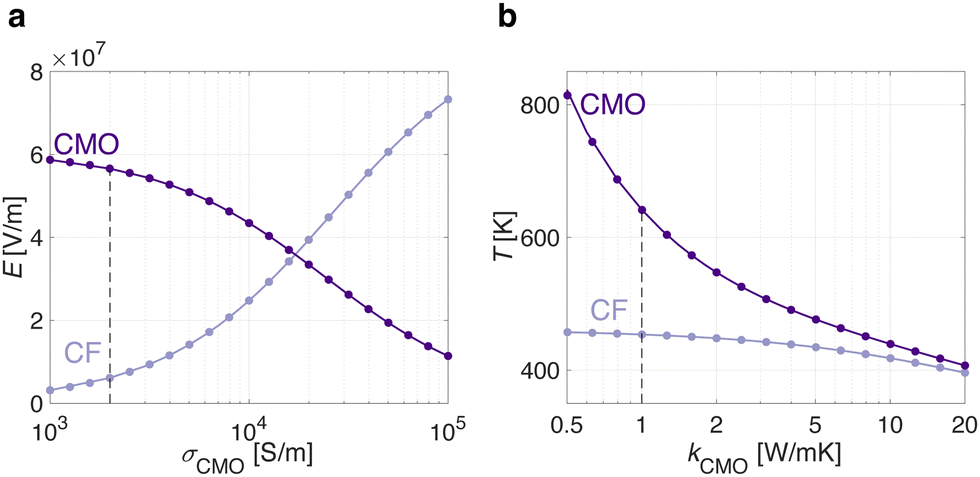
The role of the CMO layer: σCMO and kCMO
The proposed physical model is applicable to a range of analog bilayer ReRAM systems, including but not limited to TaOx/HfOx ReRAM devices. Similarly to TaOx, other CMOs can be deposited in stable sub-stoichiometric phases.21 By replacing TaOx with a designable CMO, the impact of its electrical σCMO and thermal kCMO conductivities on the average electric field and temperature distributions is assessed in CMO/HfOx ReRAM systems. To achieve this, the filament radius reported in Table 2 is used, along with a constant applied bias of V = 0.9 V on the top electrode of the CMO/HfOx ReRAM device, assumed in LRS. Considering an arbitrary constant kCMO = 1 W (m K)−1, like the one used for the TaOx layer, Fig. 4a illustrates how the effectiveness of field confinement in the CMO layer (where ECMO ≫ ECF) diminishes with the increase in CMO electrical conductivity σCMO. Similarly, considering a fixed σCMO = 2 × 10³ Sm−1, like the one used for the TaOx layer, Fig. 4b shows the thermal confinement in the CMO layer as a function of its thermal conductivity kCMO. For metallic metal-oxide, field confinement occurs within the conductive filament (ECF ≫ ECMO) and the temperature is equally distributed between the CMO and the CF, leading to the conventional abrupt switching process dominated by the CF in Ti/HfOx ReRAM device. On the other hand, properly designing the CMO as a thermal and electric field confinement layer is expected to yield an analog bilayer ReRAM device according to the physical model described in this work.
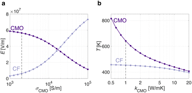 |
| | Fig. 4 Considering a filamentary CMO/HfOx ReRAM device in LRS with a constant applied bias of V = 0.9 V, the role of the electro-thermal properties of a designable CMO material is illustrated. By increasing the CMO electrical and thermal conductivity toward values typical of a metal, the spreading resistance and the resulting effectiveness of the electric field and temperature confinement in the CMO layer, decreases. The dashed lines indicate the values used in this work for the TaOx material. | |
Conclusions
Advancing the physical understanding of the resistive switching process in analog CMO/HfOx ReRAM devices is fundamental to further improving the hardware performance and enabling on-chip training of large neural network models with this technology. In this work, the first physics-based analytical current transport model of analog CMO/HfOx ReRAM devices is presented. As a case study, the model is employed to simulate experimental data from a representative analog TaOx/HfOx ReRAM device. Table 3 presents a comparison of this work with available ReRAM models in literature. Based on this work, future studies will focus on the development of a compact model description including device failure mechanisms, and subsequently circuit simulations of analog CMO/HfOx ReRAM technology.
Table 3 Comparison with available ReRAM models in literature
|
|
Bengel et al.51 |
Wu et al.22 |
Falcone et al.21 |
This work |
| Jiang et al.52 |
| Device |
ReRAM |
ReRAM |
ReRAM |
ReRAM |
| Materials |
HfOx |
TaOx/HfOx |
CMO/HfOx |
TaOx/HfOx |
| Synapse |
Digital |
Analog |
Analog |
Analog |
| Model |
Analytical |
Empirical |
Empirical |
Analytical |
| Transport |
e and  |
e
|
e
|
e and  |
| Approx. |
Compact model |
FEM |
FEM |
FEM |
In this work, it is shown that the combination of the filamentary current constriction with the electro-thermal properties of the TaOx material, enables temperature and electric field confinement in the TaOx layer. Consequently, the resistive switching is dominated by the defect dynamics in the TaOx layer rather than in the conductive filament as per conventional M/I/M ReRAM stack. The proposed analytical current transport model describes the Mott–Gurney trap-to-trap tunneling process. The resistive switching of the analog ReRAM device is attributed to the modulation of the density of defect states in the sub-band of the TaOx layer. During the RESET switching process, oxygen vacancies in the TaOx layer radially migrate toward the conductive filament, partially depleting a half-spherical volume, also known as dome. As a consequence, the lower density of defect states results in a lower electrical conductivity of the TaOx,Dome. In this process, the electric field increases while the temperature decreases. Conversely, the SET process, characterized by an exponentially increasing temperature and a nearly constant electric field, consists of a defect-enrichment of the TaOx,Dome, restoring the LRS condition. The more gradual SET of TaOx/HfOx ReRAM devices compared to conventional Ti/HfOx technology is attributed to the change from a full defect depletion/accumulation of a tiny gap in the conductive filament to a partial defect modulation in a larger TaOx,Dome. Additionally, the narrower resistive window in TaOx/HfOx ReRAM device yields a decreased temperature gradient during the SET, enhancing its graduality. The intermediate resistive states are described as a gradual increase/decrease of the TaOx,Dome defect density, which results in a variation of its electrical conductivity. The SET and RESET activation energies, extracted from the modelling of the oxygen vacancy drift dynamics, closely align with the reported oxygen vacancy migration energy in the TaOx layer. The physics-based analytical current transport model developed in this work is not limited to TaOx/HfOx devices, but applies to other similar analog CMO/HfOx ReRAM systems. Eventually, the role of the σCMO and kCMO on the electric field and temperature distributions is described, setting the groundwork for further CMO/HfOx ReRAM device optimization.
Author contributions
Conceptualization: D. F. F. and V. B.; methodology and validation: D. F. F., S. M. and V. B.; simulations: D. F. F.; result interpretation: D. F. F., S. M., M. G., T. S., V. B., A. L. P. and B. J. O.; data curation: D. F. F. and V. B.; hardware fabrication: T. S.; electrical characterization: D. F. F. and T. S.; supervision: V. B. and S. M.; manuscript writing: D. F. F.; manuscript review and editing: all authors; funding acquisition: B. J. O. and V. B.
Conflicts of interest
There are no conflicts to declare.
Acknowledgements
The authors acknowledge the Binnig and Rohrer Nanotechnology Center (BRNC) at IBM Research Europe – Zurich. This work is funded by SNSF ALMOND (grantID: 198612), by the European Union and Swiss state secretariat SERI within the H2020 MeM-Scales (grantID: 871371), MANIC (grantID: 861153) and PHASTRAC (grantID: 101092096) projects and by the Federal Ministry of Education and Research (BMBF, Germany) within the NEUROTEC (grantID: 16ME0398K) project.
References
-
B. Murmann, IEEE Transactions on Very Large Scale Integration (VLSI) Systems, 2021, vol. 29, pp. 3–13.
- A. Sebastian, M. L. Gallo, R. Khaddam-Aljameh and E. Eleftheriou, Nat. Nanotechnol., 2020, 15, 529–544 CrossRef CAS PubMed.
-
M. Horowitz, Digest of Technical Papers-IEEE International Solid-State Circuits Conference, 2014, vol. 57, pp. 10–14.
- H. Jia, M. Ozatay, Y. Tang, H. Valavi, R. Pathak, J. Lee and N. Verma, IEEE, J. Solid State Circ., 2022, 57, 198–211 Search PubMed.
-
A. Sebastian, I. Boybat, M. Dazzi, I. Giannopoulos, V. Jonnalagadda, V. Joshi, G. Karunaratne, B. Kersting, R. Khaddam-Aljameh, S. R. Nandakumar, A. Petropoulos, C. Piveteau, T. Antonakopoulos, B. Rajendran, M. L. Gallo and E. Eleftheriou, IEEE Symposium on VLSI Circuits, Digest of Technical Papers, 2019, 2019-June, pp. T168–69.
- A. Sebastian, T. Tuma, N. Papandreou, M. L. Gallo, L. Kull, T. Parnell and E. Eleftheriou, Nat. Commun., 2017, 8, 1115 CrossRef PubMed.
- S. Yin, X. Sun, S. Yu and J. S. Seo, IEEE Trans. Electron Devices, 2020, 67, 4185–4192 Search PubMed.
- R. Khaddam-Aljameh, M. Stanisavljevic, J. F. Mas, G. Karunaratne, M. Brandli, F. Liu, A. Singh, S. M. Muller, U. Egger, A. Petropoulos, T. Antonakopoulos, K. Brew, S. Choi, I. Ok, F. L. Lie, N. Saulnier, V. Chan, I. Ahsan, V. Narayanan, S. R. Nandakumar, M. L. Gallo, P. A. Francese, A. Sebastian and E. Eleftheriou, IEEE, J. Solid State Circ., 2022, 57, 1027–1038 Search PubMed.
-
P. Deaville, B. Zhang and N. Verma, Digest of Technical Papers - Symposium on VLSI Technology, 2022, 2022-June, pp. 268–269.
- M. L. Gallo, R. Khaddam-Aljameh, M. Stanisavljevic, A. Vasilopoulos, B. Kersting, M. Dazzi, G. Karunaratne, M. Brändli, A. Singh, S. M. Müller, J. Büchel, X. Timoneda, V. Joshi, M. J. Rasch, U. Egger, A. Garofalo, A. Petropoulos, T. Antonakopoulos, K. Brew, S. Choi, I. Ok, T. Philip, V. Chan, C. Silvestre, I. Ahsan, N. Saulnier, V. Narayanan, P. A. Francese, E. Eleftheriou and A. Sebastian, Nat. Electron., 2023, 6, 680–693 CrossRef.
- R. Khaddam-Aljameh, M. Martemucci, B. Kersting, M. L. Gallo, R. L. Bruce, M. Brightsky and A. Sebastian, IEEE Trans. Circuits Syst., 2021, 68, 3522–3526 Search PubMed.
- G. W. Burr, R. M. Shelby, A. Sebastian, S. Kim, S. Kim, S. Sidler, K. Virwani, M. Ishii, P. Narayanan, A. Fumarola, L. L. Sanches, I. Boybat, M. L. Gallo, K. Moon, J. Woo, H. Hwang and Y. Leblebici, Adv. Phys.: X, 2017, 2, 89–124 Search PubMed.
-
S. Jain, H. Tsai, C. T. Chen, R. Muralidhar, I. Boybat, M. M. Frank, S. Wozniak, M. Stanisavljevic, P. Adusumilli, P. Narayanan, K. Hosokawa, M. Ishii, A. Kumar, V. Narayanan and G. W. Burr, IEEE Transactions on Very Large Scale Integration (VLSI) Systems, 2023, vol. 31, pp. 114–127.
- T. Gokmen and W. Haensch, Front. Neurosci., 2020, 14, 103 CrossRef PubMed.
- G. W. Burr, M. J. BrightSky, A. Sebastian, H. Y. Cheng, J. Y. Wu, S. Kim, N. E. Sosa, N. Papandreou, H. L. Lung, H. Pozidis, E. Eleftheriou and C. H. Lam, IEEE J. Emerging Sel. Top. Circuits Syst., 2016, 6, 146–162 Search PubMed.
- D. Ielmini, Semicond. Sci. Technol., 2016, 31, 063002 CrossRef.
- T. Gokmen and Y. Vlasov, Front. Neurosci., 2016, 10, 333 Search PubMed.
-
N. Gong, M. J. Rasch, S. C. Seo, A. Gasasira, P. Solomon, V. Bragaglia, S. Consiglio, H. Higuchi, C. Park, K. Brew, P. Jamison, C. Catano, I. Saraf, F. F. Athena, C. Silvestre, X. Liu, B. Khan, N. Jain, S. McDermott, R. Johnson, I. Estrada-Raygoza, J. Li, T. Gokmen, N. Li, R. Pujari, F. Carta, H. Miyazoe, M. M. Frank, D. Koty, Q. Yang, R. Clark, K. Tapily, C. Wajda, A. Mosden, J. Shearer, A. Metz, S. Teehan, N. Saulnier, B. J. Offrein, T. Tsunomura, G. Leusink, V. Narayanan and T. Ando, Technical Digest - International Electron Devices Meeting, IEDM, 2022, 2022-December, pp. 33.7.1–33.7.4.
- Y. Kim, S. C. Seo, S. Consiglio, P. Jamison, H. Higuchi, M. Rasch, E. Y. Wu, D. Kong, I. Saraf, C. Catano, R. Muralidhar, S. Nguyen, S. Devries, O. V. D. Straten, M. Sankarapandian, R. N. Pujari, A. Gasasira, S. M. McDermott, H. Miyazoe, D. Koty, Q. Yang, H. Yan, R. Clark, K. Tapily, S. Engelmann, R. R. Robison, C. Wajda, A. Mosden, T. Tsunomura, R. Soave, N. Saulnier, W. Haensch, G. Leusink, P. Biolsi, V. Narayanan and T. Ando, IEEE Electron Device Lett., 2021, 42, 759–762 CAS.
- D. Ielmini, S. Balatti, S. Larentis, D. C. Gilmer and F. Nardi, IEEE Trans. Electron Devices, 2012, 59, 20812–20818 Search PubMed.
-
D. F. Falcone, S. Menzel, T. Stecconi, A. L. Porta, L. Carraria-Martinotti, B. J. Offrein and V. Bragaglia, 2023 IEEE International Memory Workshop, IMW 2023 - Proceedings, 2023, pp. 1–4.
- W. Wu, H. Wu, B. Gao, N. Deng, S. Yu and H. Qian, IEEE Electron Device Lett., 2017, 38, 1 CAS.
-
D. C. Sekar, B. Bateman, U. Raghuram, S. Bowyer, Y. Bai, M. Calarrudo, P. Swab, J. Wu, S. Nguyen, N. Mishra, R. Meyer, M. Kellam, B. Haukness, C. Chevallier, H. Wu, H. Qian, F. Kreupl and G. Bronner, Technical Digest - International Electron Devices Meeting, IEDM, 2015, 2015-February, pp. 28.3.1–28.3.4.
- T. Stecconi, V. Bragaglia, M. J. Rasch, F. Carta, F. Horst, D. F. Falcone, S. C. ten Kate, N. Gong, T. Ando, A. Olziersky and B. Offrein, Nano Lett., 2024, 24, 866–872 CrossRef CAS PubMed.
-
T. Stecconi, Y. Popoff, R. Guido, D. Falcone, M. Halter, M. Sousa, F. Horst, A. L. Porta, B. J. Offrein and V. Bragaglia, European Solid-State Device Research Conference, 2022, 2022-September, pp. 297–300.
- T. Stecconi, R. Guido, L. Berchialla, A. L. Porta, J. Weiss, Y. Popoff, M. Halter, M. Sousa, F. Horst, D. Dávila, U. Drechsler, R. Dittmann, B. J. Offrein and V. Bragaglia, Adv. Electron. Mater., 2022, 8, 2200448 CrossRef CAS.
- M. Abedin, N. Gong, K. Beckmann, M. Liehr, I. Saraf, O. V. der Straten, T. Ando and N. Cady, Sci. Rep., 2023, 13, 14963 CrossRef CAS PubMed.
- K. Bao, J. Meng, J. D. Poplawsky and M. Skowronski, J. Non-Cryst. Solids, 2023, 617, 122495 CrossRef CAS.
- T. V. Perevalov, V. A. Gritsenko, S. B. Erenburg, A. M. Badalyan, H. Wong and C. W. Kim, J. Appl. Phys., 2007, 101, 053704 CrossRef.
- L. Zhu, J. Zhou, Z. Guo and Z. Sun, J. Phys. Chem. C, 2016, 120, 2456–2463 CrossRef CAS.
- C. Funck and S. Menzel, ACS Appl. Electron. Mater., 2021, 3, 3674–3692 CrossRef CAS.
- I. Goldfarb and R. S. Williams, Appl. Phys. A: Mater. Sci. Process., 2014, 114, 287–289 CrossRef CAS.
- C. E. Graves, N. Dávila, E. J. Merced-Grafals, S. T. Lam, J. P. Strachan and R. S. Williams, Appl. Phys. Lett., 2017, 110, 123501 CrossRef.
-
N. F. Mott and R. W. Gurney, Electronic processes in ionic crystals, Oxford at theClarendon Press, 2 edn, 1950 Search PubMed.
- C. L. Torre, A. F. Zurhelle, T. Breuer, R. Waser and S. Menzel, IEEE Trans. Electron Devices, 2019, 66, 1268–1275 Search PubMed.
- W. S. Lew, D. J. Loy, P. A. Dananjaya, S. Chakrabarti, K. H. Tan, S. C. Chow and E. H. Toh, ACS Appl. Electron. Mater., 2020, 2, 3160–3170 CrossRef.
- J. H. Hur, Sci. Rep., 2019, 9, 17019 CrossRef PubMed.
-
C. L. T. Beechem, Thermal Transport in TaOxFilms for Memristive Applications, https://www.osti.gov/servlets/purl/1260377/, 2015.
- M. A. Panzer, M. Shandalov, J. A. Rowlette, Y. Oshima, Y. W. Chen, P. C. McIntyre and K. E. Goodson, IEEE Electron Device Lett., 2009, 30, 1269–1271 CAS.
- C. Y. Ho, R. W. Powell and P. E. Liley, J. Phys. Chem. Ref. Data, 2009, 1, 279–421 CrossRef.
- A. A. Irudayaraj, R. Srinivasan, P. Kuppusami, E. Mohandas, S. Kalainathan and K. Ramachandran, J. Mater. Sci., 2008, 43, 1114–1120 CrossRef CAS.
- U. I. Bature, I. M. Nawi, M. H. M. Khir, F. Zahoor, A. S. Algamili, S. S. Hashwan and M. A. Zakariya, Materials, 2022, 15, 1205 CrossRef CAS PubMed.
-
C. H. Kuo, V. Wang, Z. Zhang, J. Spiegelman, D. Alvarez, A. C. Kummel, S. U. Yun and H. Simka, 2021 IEEE International Interconnect Technology Conference, IITC 2021, 2021, pp. 1–3.
- W. Kim, S. Menzel, D. J. Wouters, Y. Guo, J. Robertson, B. Roesgen, R. Waser and V. Rana, Nanoscale, 2016, 8, 17774–17781 RSC.
-
L. Goux, A. Fantini, A. Redolfi, C. Y. Chen, F. F. Shi, R. Degraeve, Y. Y. Chen, T. Witters, G. Groeseneken and M. Jurczak, Digest of Technical Papers - Symposium on VLSI Technology, 2014, pp. 1–2.
-
A. Padovani, L. Larcher, P. Padovani, C. Cagli and B. D. Salvo, 2012 4th IEEE International Memory Workshop, IMW 2012, 2012, pp. 1–4.
- A. Padovani, L. Larcher, G. Bersuker and P. Pavan, IEEE Electron Device Lett., 2013, 34, 680–682 CAS.
- S. H. Lee, J. Kim, S. J. Kim, S. Kim and G. S. Park, Phys. Rev. Lett., 2013, 110, 235502 CrossRef PubMed.
- Y. Guo and J. Robertson, Appl. Phys. Lett., 2014, 104, 112906 CrossRef.
- N. Sommer, R. Dittmann and S. Menzel, Phys. Rev. Appl., 2023, 19, 044084 CrossRef CAS.
- C. Bengel, A. Siemon, F. Cüppers, S. Hoffmann-Eifert, A. Hardtdegen, M. V. Witzleben, L. Hellmich, R. Waser and S. Menzel, IEEE Trans. Circuits Syst., 2020, 67, 4618–4630 Search PubMed.
- Z. Jiang, Y. Wu, S. Yu, L. Yang, K. Song, Z. Karim and H. S. Wong, IEEE Trans. Electron Devices, 2016, 63, 1884–1892 CAS.
|
| This journal is © The Royal Society of Chemistry 2024 |
Click here to see how this site uses Cookies. View our privacy policy here. 
 Open Access Article
 This Open Access Article is licensed under a
  *a,
Stephan
Menzel
*a,
Stephan
Menzel

 , which have been reported to generally have lower formation and migration energies with respect to Tai interstitials.29,30 Each double-positively charged vacancy
  generates two electronic defect states in the band gap.30 Therefore, the maximum density of defect states Nmaxe that may contribute to the transport can be related to the ionic vacancy concentration
  , according to
  . Depending on the energy alignment between the defect sub-band in the TaOx layer and the Fermi level of the electrodes, statistically only a sub-set of the defect states Ne contributes to the electronic transport, resulting in eqn (2).
 in the TaOx layer during the SET and RESET processes is similarly described by an ion-hopping conduction over a migration energy barrier ΔEion,35 according to eqn (3) and (4),
 is the charge number of the oxygen vacancies relative to the perfect crystal, aion is the crystal hopping distance and ν0,ion is the ion attempt frequency.


 during the SET and RESET transitions is modelled. For each voltage step (10 mV) during the SET and RESET processes, the average oxygen vacancy drift velocity is computed according to eqn (3). By scaling the drift velocity with the experimental measurement time (100 ms per step), an average drift induced displacement is computed for each voltage step. The cumulative sum of the displacements during both the SET and RESET transitions, results in the average size of the dome along the vertical direction. For consistency with the current transport model (see Fig. 2), an overall oxygen vacancy displacement of approximately 10 nm is assumed for both the SET and RESET, while the ion-hopping energy barriers ΔEion,SET and ΔEion,RESET are considered as fitting parameters. The extracted ion activation energies are ΔEion,RESET = 1.44 eV and ΔEion,SET = 1.32 eV. Consistently, both energies closely align with the reported oxygen vacancy migration energy of ≈1.5 eV30 in the TaOx layer. The difference between ΔEion,RESET and ΔEion,SET may suggest that the two migrations happen through different energy paths. Oxygen vacancy accumulation at the interface with the conductive filament (during RESET) may require more energy than redistribution back into the 3D half-spherical volume (during SET). Fig. 3e and f show the oxygen vacancy drift velocity and the resulting ionic current scaled by the β factor, according to eqn (4), during the quasi-static SET and RESET, respectively. Although the β factor, which describes the sub-set of defect states contributing to conduction, may vary during the switching process, the change in βIdriftion is primarily attributed to a change in Idriftion, which depends on the electro-thermal conditions according to eqn (4). In agreement with the experimental switching characteristic, the ionic drift dynamics follow an exponentially increasing trend during SET (see Fig. 3e) and a nearly uniform one during RESET (see Fig. 3f). Future work will focus on establishing the analytical link between the
  average drift velocity and the ionic vacancy concentration
  , which determines the electronic current according to eqn (1) and (2). Although not included in this work, the competing ionic diffusion and the reaching of a saturation of the oxygen vacancy concentration in the TaOx layer, are expected to mitigate and eventually stop the drift dynamics. Compared to conventional Ti/HfOx ReRAM technology, the proposed model of a TaOx/HfOx ReRAM device shows a similar intrinsically gradual RESET, but a fundamentally different SET, from abrupt to exponential. The graduality of the SET process is explained by a new physical interpretation, from a full defect depletion/accumulation of a tiny gap in the HfOx filament to a partial modulation of defects in a larger 3D half-spherical shape in the TaOx layer. Additionally, the narrower resistive window (typically <10)24 in TaOx/HfOx ReRAM devices yields a decreased temperature gradient during SET, enhancing its graduality.