
 Open Access Article
 This Open Access Article is licensed under a
 Creative Commons Attribution 3.0 Unported Licence
Reliability effects of lateral filament confinement by nano-scaling the oxide in memristive devices†
Pascal
Stasner
 *a,
Nils
Kopperberg‡
a,
Kristoffer
Schnieders‡
b,
Tyler
Hennen
a,
Stefan
Wiefels
b,
Stephan
Menzel
b,
Rainer
Waser
abc and
Dirk J.
Wouters
a
*a,
Nils
Kopperberg‡
a,
Kristoffer
Schnieders‡
b,
Tyler
Hennen
a,
Stefan
Wiefels
b,
Stephan
Menzel
b,
Rainer
Waser
abc and
Dirk J.
Wouters
a
aInstitut für Werkstoffe der Elektrotechnik II (IWE2) and JARA-FIT, RWTH Aachen University, Aachen 52074, Germany. E-mail: stasner@iwe.rwth-aachen.de
bPeter-Grünberg-Institut 7 (PGI-7), Forschungszentrum Jülich GmbH, Jülich 52425, Germany
cPeter-Grünberg-Institut 10 (PGI-10), Forschungszentrum Jülich GmbH, Jülich 52425, Germany
First published on 15th March 2024
Abstract
Write-variability and resistance instability are major reliability concerns impeding implementation of oxide-based memristive devices in neuromorphic systems. The root cause of the reliability issues is the stochastic nature of conductive filament formation and dissolution, whose impact is particularly critical in the high resistive state (HRS). Optimizing the filament stability requires mitigating diffusive processes within the oxide, but these are unaffected by conventional electrode scaling. Here we propose a device design that laterally confines the switching oxide volume and thus the filament to 10 nm, which yields reliability improvements in our measurements and simulations. We demonstrate a 50% decrease in HRS write-variability for an oxide nano-fin device in our full factorial analysis of modulated current–voltage sweeps. Furthermore, we use ionic noise measurements to quantify the HRS filament stability against diffusive processes. The laterally confined filaments exhibit a change in the signal-to-noise ratio distribution with a shift to higher values. Our complementing kinetic Monte Carlo simulation of oxygen vacancy (re-)distribution for confined filaments shows improved noise behavior and elucidates the underlying physical mechanisms. While lateral oxide volume scaling down to filament sizes is challenging, our efforts motivate further examination and awareness of filament confinement effects in regards to reliability.
New conceptsConventional scaling of memristive devices focuses mostly on reducing just the electrode area. Here, we laterally scale the oxide to filament size and passivate the immediate filament surrounding with a diffusion barrier. Our oxide nano-fin memristive device concept, which laterally confines the switching oxide in one dimension, enables more control over the random nature of conductive filament formation. Specifically, the design allows us to examine the effects of laterally confining filament broadening through oxygen vacancy diffusion. Reliability improvements from the manipulation of filament properties in these oxide-scaled devices are demonstrated by electrical measurements. Respective physical simulations support our findings. We promote a focus shift from the prevalent electrode scaling to oxide volume scaling by highlighting the importance of limiting diffusive processes within the oxide that go beyond the influence of just electrode scaling. We believe that controlling filament properties through confinement is an important step towards mitigation of the reliability concerns regarding memristive devices in neuromorphic systems. Here, the benefits of our device design functions in addition and complementary to previous electrical and material optimization concepts. |
Introduction
Latency and power demand of data transfer between processing and memory increasingly limit computing performance of artificial intelligence related tasks, like image classification and speech recognition.1,2 Neuromorphic systems aim to mitigate this bottleneck in conventional von Neumann architectures by mimicking the close interconnection of processing and memory in the energy-efficient human brain. Non-von Neumann approaches like computation-in-memory can use memristive devices as adjustable weights in neural nets, inspired by the function of biological synapses.3,4 One promising kind of memristive device is the oxide-based valence-change memory (VCM), where a voltage-controlled oxygen-deficient filamentary region determines the conductance state of the device.5–7 Hardware-implemented non-von Neumann architectures based on these devices have successfully been demonstrated.8,9 However, reliability concerns regarding write-variability and conductance state instability are key challenges impeding further progress and industrial-scale adoption.10–16These reliability problems stem from the inherent randomness of filament formation and the respective oxygen vacancy distribution. Scaling the device dimensions is a viable method to gain partial control over filament formation, but requires scaling beyond common filament sizes to affect its properties. Reported lateral filament dimensions vary across a wide range from several hundreds of nanometers down to a few nanometers. Studies using X-ray photoelectron emission spectroscopy (XPEEM) identified filament dimensions of 200 nm to 500 nm in SrTiO3 and 70 nm in TaOx.17–19 Hewlett-Packard Laboratories carried out other X-ray-based observational methods, which yielded filament sizes of 150 nm to 300 nm.20–22 Celano et al. used scanning probe microscopy (SPM) to spatially resolve the filament and reported areas of 103 nm2 to 104 nm2 in TaOx and smaller filaments of 102 nm2 to 103 nm2 in HfOx.23,24 Similarly, Rao et al. depict a 20 nm filament by conductive atomic force microscopy (C-AFM).25 Kwon et al. used transmission electron microscopy (TEM) imaging to measure 15 nm26 and 20 nm27 filaments, also reporting coexistence of stronger filaments within the device. Further studies used TEM-related analysis and electron energy loss spectroscopy (EELS) to reveal filament sizes of 10 nm to 50 nm.28–33
Evidently, various filament sizes and shapes are reported throughout the literature as filament formation depends on many electrical characteristics (forming voltage, parasitic capacitance, current compliance and current overshoot34) and material properties. Industrially optimized cells in 1T1R configuration, as reported by Panasonic with filament dimensions of 10 nm to 25 nm,29–31 likely result in more controlled filament formation with thinner filaments. Therefore, advanced demands on scaling to 10 nm and beyond is required for inducing filament confinement effects.
Many reports show successful fabrication of nano-scaled cross-bar devices by lithographic scaling of the electrodes.35–40 However, this method encounters reliability issues beyond line resolutions of around 30 nm. Lithographically scaled via41–44 and pillar etching10,30 face the same challenges. Partial lateral inactivation of the lithographically scaled ohmic electrode (OE) by thermal oxidation is reported to enable reduction of the electrode width down to 10 nm.30,45,46 Further reliable scaling requires a method not based on overcoming lithographic line resolutions. Here, three-dimensional structures are utilized to define cell dimension by electrode film thickness.47–51 Li et al. and Pi et al. demonstrate the superior scalability of this method with sub-3 nm electrodes.47,48 A tabular overview of the referenced nano-scaling literature is depicted in the ESI† (see Fig. S1).
All these device scaling methods revolve around reduction of the overlapping electrode area with previous studies predominantly focusing on scaling the electrode part of memristive devices. While electrode scaling is already successfully demonstrated in numerous ways, none of the previously mentioned studies laterally scales the oxide to 10 nm or less. So far, retention improvements from lateral oxide encapsulation with an oxygen diffusion barrier could already be demonstrated by Hayakawa et al. and Yu et al., despite comparably large oxide dimensions of >50 nm.30,50 However, the associated effects of direct filament confinement in oxides scaled down to 10 nm or less remain unresolved.
In this work, we propose a device design for enabling lateral filament confinement to 10 nm in oxide-based memristive devices. We encapsulate the nano-scaled oxide in a passivation material, acting as a barrier for lateral oxygen (vacancy) diffusion. We conduct electrical measurements on the fabricated devices to investigate the effects of filament confinement on critical reliability concerns like HRS write-variability and resistance instability. Our simulations of oxygen vacancy (re-)distribution in unconfined and confined filaments provide further insight into the underlying physical mechanisms of the observed reliability enhancements.
Results and discussion
Nano-device fabrication and concept
Fig. 1 depicts microscopy images after the main fabrication steps of the nano-fin device, where the switching oxide volume and the ohmic electrode are laterally confined to 10 nm in one dimension. We use reactive ion etching (RIE) with CHF3 to form a shallow trench with a depth of 65 nm in an insulating 200 nm thick silicon nitride (SiN) film deposited on a silicon substrate by plasma-enhanced chemical vapor deposition (PECVD). Fig. 1(a) shows a scanning electron microscopy (SEM) picture of the cross-section of the etched trench after the silicon substrate is cleaved across the trench width. The depicted edge of the trench features a vertical sidewall angle and low line edge roughness. Subsequently, 20 nm of ohmic electrode material is sputter-deposited onto the sample (see Fig. 1(b)), lining the trench with a thin layer of electrode material. Here, we used tantalum (Ta). Due to the slower deposition rate on vertical surfaces, the electrode film on the sidewall of the trench measures 10 nm horizontally. However, higher deposition rate and a resulting thicker electrode coverage on the bottom of the trench in combination with wide trench dimensions improve the conductance of the nano-scaled electrode. The remaining trench depth after electrode deposition is filled with passivating SiN, aiming to at least cover the initial trench depth of 65 nm with the deposited Ta/SiN film stack. Chemical-mechanical polishing (CMP) on a polyurethane pad planarizes the sample surface, removing protruding material from the surface at a rate of 13 nm/min until the 10 nm thin electrode fin on the trench sidewall is exposed at the surface (see Fig. 1(c)).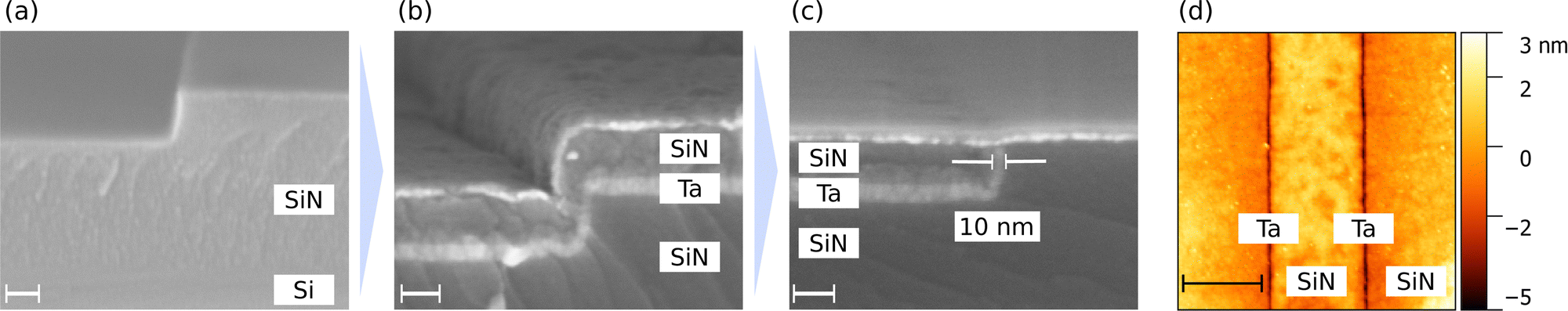 | ||
| Fig. 1 (a)–(c) SEM cross-sectional views of the initial fabrication steps of the nano-fin device. (a) 65 nm deep trench etched into passivating SiN. (b) The trench is filled with 20 nm Ta and 45 nm SiN. (c) After planarization of the surface protrusions by CMP, the Ta-fin on the sidewall is exposed at the surface, embedded between SiN. The lateral width of the sputtered electrode fin is 10 nm. Here, the sample surface is covered with a 5 nm conductive coating to enable good imaging by SEM. All SEM scale bars are 40 nm. (d) Top-view AFM scan of a filled 2.4 μm wide trench after planarization. The trench edge is lined with the electrode fin. The AFM scale bar is 2 μm. | ||
The height profile after planarization of the device is measured with atomic force microscopy (AFM). The top-view scan (see Fig. 1(d)) shows a planarized 2.4 μm wide trench expanding along the vertical direction, while the circumference of the trench is lined with a 10 nm Ta-fin. The focus of this study is to examine the effects of oxide scaling, rather than array density scaling. Therefore, a comparably large trench width of 2.4 μm is chosen for simplifying the process flow but we expect this approach to scale to <100 nm. The electrode fin is laterally embedded within SiN and lies 2 nm below the surrounding surface, due to higher CMP material removal rate around the Ta-fin compared to SiN (see AFM line scan in Fig. S2, ESI†). The undesirable effect of CMP-dishing is prevented by using trench widths of <3 μm. For larger trench widths, dishing removes the passivating SiN in the center of the trench, exposing the Ta-coating in extreme cases. We aim for at least 35 nm of remaining SiN in the center of the trench for electrical passivation of the buried Ta-coating.
Fig. 2(a) visualizes the fabricated structure schematically. This use of sidewall technology with CMP allows for extreme scalability of the Ta nano-fin beyond conventional lithographic resolution limits, as finely tunable film thickness during electrode deposition defines the lateral resolution of the fin. Li et al.47 present the ability to scale TiN electrodes to sub-5 nm by sidewall technology and Pi et al.48 use a similar approach to create 2 nm platinum (Pt) electrode fins. However, in their studies the oxide is deposited on the entire planarized surface of the sample, yielding a confined electrode but an entirely unconfined switching oxide.
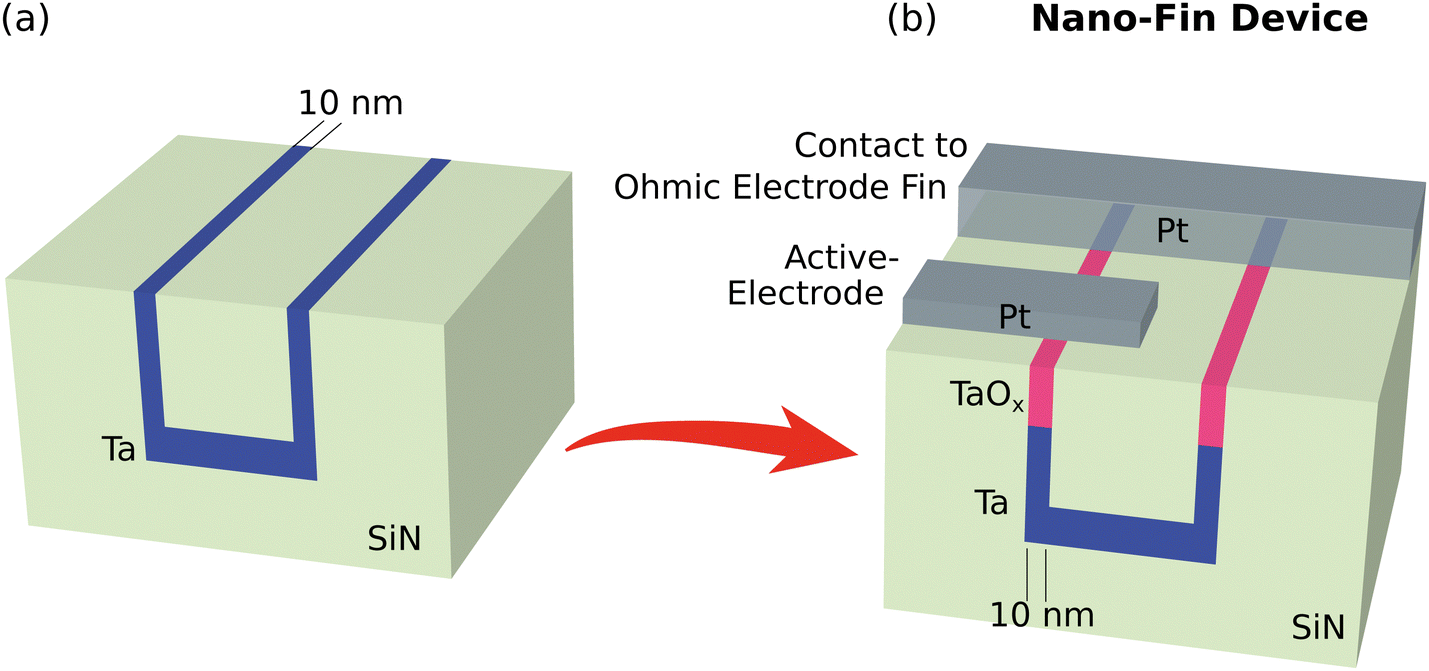 | ||
| Fig. 2 (a) Schematic illustration of the finished structure from Fig. 1 as starting point for further fabrication. (b) Deposition of the upper Pt-pad for directly contacting the ohmic electrode (Ta-fin), followed by oxidation of the remaining Ta electrode fin surface and deposition of a nano-scaled Pt active electrode complete the fabrication. The oxide nano-fin is laterally confined in one dimension and encapsulated by SiN. | ||
In our process, we specifically use easily oxidizable ohmic electrode material for fabrication of the nano-fin, which in combination with a bottom-up technology like thermal oxidation enables us to embed the switching oxide within the oxidation-resistant SiN (see Fig. 2(b)).52 A preceding Pt electrode deposition (with Argon in situ etching) allows for electrical contact of the nano-fin followed by thermal or native oxide growth of the remaining exposed electrode fin, which has a high oxygen affinity. This bottom-up approach adds the benefit of damage-free oxide growth, as Hayakawa et al. show that introducing free oxygen radicals and their diffusion into the filament degrade the retention.30 Finally, a 150 nm wide Pt top electrode is sputter-deposited and structured by electron beam lithography, acting as the active electrode (AE) to complete fabrication of the Ta/TaOx/Pt resistive switching nano-fin device with highly scaled oxide and ohmic electrode.
Reliability improvements in nano-fin device
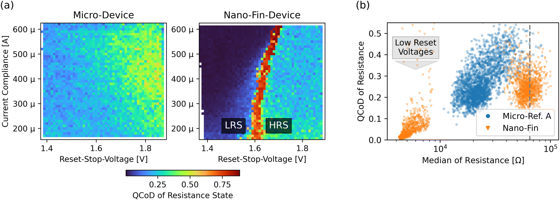
We analyze the write-variability of the oxide nano-fin device and a micro-sized reference device ‘A’ (details in methods section) by stressing the cells with 100![[thin space (1/6-em)]](https://www.rsc.org/images/entities/char_2009.gif) 000 parametrized current–voltage (I–V) sweeps. We use our customized measurement setup for the full factorial analysis, further described in the methods section, with 2500 unique parameter combinations of current compliance (CC) and RESET-stop-voltage Vreset,stop, which is defined as the maximum voltage amplitude at the RESET polarity. Here, Vreset,stop is an external control parameter not to be confused with Vreset, which marks the characteristic onset of the RESET transition. The I–V sweeps of the reference micro-device and the oxide nano-fin device are depicted in the ESI† (Fig. S3 and S4). We extract the median resistance state after the RESET sweep for each of the 2500 control parameters (see Fig. S5, ESI†). The oxide nano-fin device needs higher applied voltages (>1.6 V) for RESET from the low-resistance-state (LRS) into the HRS due to voltage drop across nano-scaled electrodes. The nano-fin shows reliable RESET into high HRS of around 65 kΩ for sufficiently high Vreset,stop. In comparison, lower Vreset,stop already weakly RESETs the reference device into low HRS of <20 kΩ. However, the reference device requires higher Vreset,stop values than the nano-fin device to RESET into comparable HRS of 65 kΩ.
000 parametrized current–voltage (I–V) sweeps. We use our customized measurement setup for the full factorial analysis, further described in the methods section, with 2500 unique parameter combinations of current compliance (CC) and RESET-stop-voltage Vreset,stop, which is defined as the maximum voltage amplitude at the RESET polarity. Here, Vreset,stop is an external control parameter not to be confused with Vreset, which marks the characteristic onset of the RESET transition. The I–V sweeps of the reference micro-device and the oxide nano-fin device are depicted in the ESI† (Fig. S3 and S4). We extract the median resistance state after the RESET sweep for each of the 2500 control parameters (see Fig. S5, ESI†). The oxide nano-fin device needs higher applied voltages (>1.6 V) for RESET from the low-resistance-state (LRS) into the HRS due to voltage drop across nano-scaled electrodes. The nano-fin shows reliable RESET into high HRS of around 65 kΩ for sufficiently high Vreset,stop. In comparison, lower Vreset,stop already weakly RESETs the reference device into low HRS of <20 kΩ. However, the reference device requires higher Vreset,stop values than the nano-fin device to RESET into comparable HRS of 65 kΩ.
Fig. 3(a) compares the HRS write-variability of the reference micro-device with the oxide nano-fin device for all control parameters. We use the quartile coefficient of dispersion  as a measure of normalized variability, where Q1 and Q3 refer to the first and third quartiles of the resistance states. Larger variability (dispersion) in a dataset results in a higher QCoD value. The HRS variability in the micro-device increases for higher Vreset,stop voltages, reaching QCoD values of around 0.5. The nano-fin device shows the unstable transition from unsuccessful to successful RESETs at Vreset,stop values of around 1.6 V. For successful RESETs at >1.6 V, the HRS variability of the nano-fin with QCoD-values of around 0.25 is lower than in the micro-device. The decrease in variability is also evident in the I–V sweeps (see Fig. S3 and S4, ESI†).
 | ||
| Fig. 3 (a) Comparison between the micro-device and nano-fin device regarding the write-variability of resistance states after RESET-sweeps for each of the 50 × 50 control parameters. Higher values of quartile coefficient of dispersion (QCoD) indicate higher variability. (b) Write-variability of the resistance state in dependence of the median resistance state after RESET for the 2500 control parameter combinations. The reference micro-device (blue) and the nano-fin device (orange) both show trends of higher variability for higher resistance states. The nano-fin device values have a lower variability for comparable resistance states (dashed line). | ||
Fig. 3(b) depicts the QCoD of resistance states for all 2500 unique control parameters in dependence of the respective median resistance after the RESET sweeps. We observe a trend of increasing HRS variability for higher median HRS values, as expected from a lower oxygen vacancy concentration and a corresponding larger impact on resistance change for minor redistribution of vacancies. Extrapolating the variability increase of the reference micro-device (blue) to an HRS of 65 kΩ (dashed line) results in a QCoD value of around 0.55. For the same resistance state, the oxide nano-fin device (orange) with the laterally confined filament shows a variability reduction of ∼50% to a QCoD value of around 0.25. The partial one-dimensional filament confinement in the nano-fin may already limit filament broadening and lateral vacancy diffusion. Thus, fewer available filament states and shapes could be the cause for more reproducible write-operations for any given resistance state.
Surrounding architecture effects, like different parasitic capacitance or series resistance, can influence the device behavior during dynamic I–V sweeps53 when comparing scaled and unscaled devices. To enable optimal comparison of our devices, we conduct ionic noise measurements (see methods section), as filament resistance instability is unaffected by the previously mentioned architecture-specific effects.
Fig. 4(a) depicts the extracted signal-to-noise ratios (SNR, defined in methods section) from HRS current traces with a median read current between 1 μA and 10 μA. The trace measurements are repeated in-between full SET-RESET cycles, yielding an accumulated trace duration of 1700 to 8000 seconds for each device. We measure the ionic noise for 2 seconds immediately following the RESET, as this has been shown to be the most critical timeframe in regards to noise.54,55 The SNR values are plotted on a logarithmic scale against the standard normal quantiles. Higher SNR values indicate a desirable reduction of ionic noise. Here, we compare the SNR values of the nano-fin device (orange) with three micro-scaled reference devices described in the methods section. Despite different thermal oxidation parameters of the micro-devices, yielding various oxide thicknesses and series resistances, the distribution function of their SNR values are in close agreement. The linear trend for the micro-sized reference cell distributions indicates conformity to a log-normal distribution. Schnieders et al. also reported the same log-normal behavior for HfOx-based nano-devices, where electrode scaling down to 100 nm did not change the distribution function.56 In contrast, the SNR values of the scaled oxide nano-fin start to deviate from the log-normal distribution to improved SNR at >0.5σ (upper 30% of all SNR values). At >2σ, the SNR values are over two times higher than the reference micro-devices. However, the nano-fin device behaves similar to the reference devices in worst-case scenarios with lower SNR values.
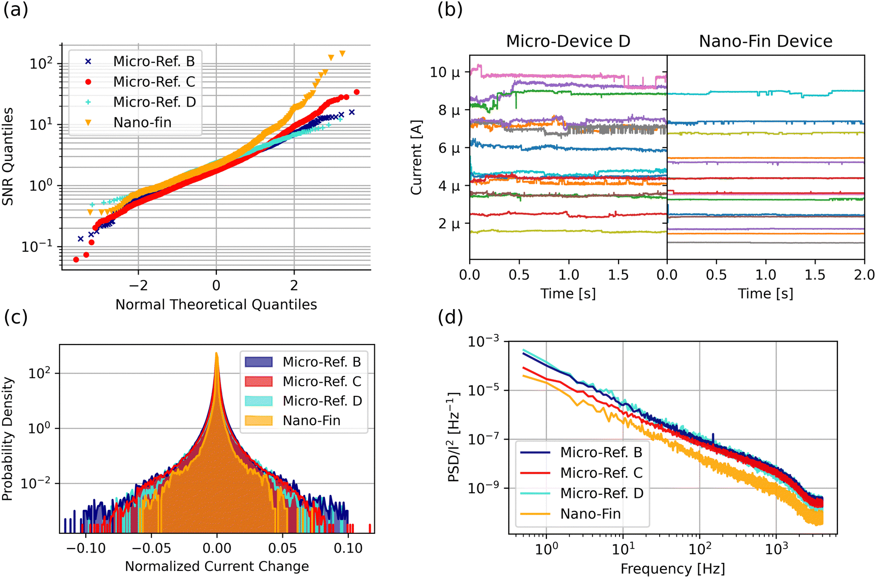 | ||
| Fig. 4 (a) Signal-to-noise ratio of current traces plotted against the quantiles of a normal distribution. 30% of all nano-fin current traces (orange) deviate from the log-normal distribution to improved SNR. (b) Noise comparison of the best 15 current traces for the micro-sized reference device and the nano-fin device. (c) Logarithmic histogram of all normalized current changes between consecutive measurement time steps from the best 5% traces. The envelope of the nano-fin histogram (orange) shows a decrease in occurrence across various current change amplitudes compared to the reference micro-devices. (d) Current-normalized power spectral density of the best 5% traces. The noise signal of the nano-fin device (orange) is shifted to lower values for all frequencies. | ||
We examine the noise characteristics of the best-case scenarios to understand the physical origin of ionic noise improvement in the partially confined oxide nano-fin device. Fig. 4(b) compares the best HRS current traces in regards to SNR of a reference micro-device with the nano-fin device. Ionic noise causes abrupt current changes during a constant voltage read with a duration of two seconds. The current traces in the micro-device jump between multiple levels and some traces show a gradual current drift, resulting in the overlap of different traces. In contrast, the current traces of the nano-fin device do not exhibit current drift and show smaller current jumps between only a few levels, suggesting fewer available filament states.
A logarithmic histogram of the normalized current changes between consecutive measurement time steps in Fig. 4(c) depicts all observed current differences of the signal and the lagged signal. Here, large relative current changes originate from vacancy diffusion close to the filament-gap interface and smaller current changes from diffusion within the filament.54 When comparing the best 5% traces (>1.65σ) of the nano-fin and the reference devices, we observe a decrease of the distribution tail end to lower maximum current change amplitude. Furthermore, less severe current changes of <0.03 occur less frequently in the nano-fin. In accordance with Fig. 4(a), the histogram envelope of the nano-fin continuously approaches the distribution of reference cells when including traces with worse SNR (see Fig. S6, ESI†).
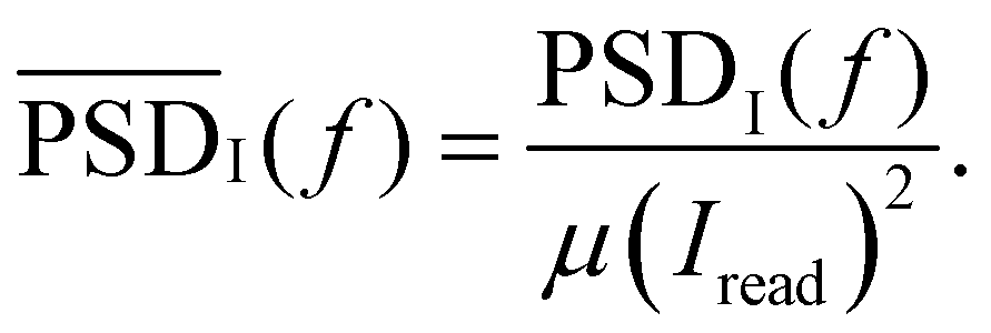
In Fig. 4(d) we depict the frequency-resolved ionic noise of the best 5% traces in form of a power spectral density (PSD), which we normalized by the median read current (for best 50% traces see Fig. S7, ESI†). The PSD from the nano-fin device reveals a decrease of the 1/fα noise spectrum across all measured frequencies. Yu et al. report this same shift in noise behavior for transition from HRS to LRS.57 In the nano-fin device, we observe this shift towards LRS-behavior despite being in the same resistance range as the reference devices.
C-AFM imaging of filaments in recent work by Rao et al. revealed that higher-resistive incomplete channels at the outer filament fringe are the major contributors to ionic noise.25 We believe that the observed SNR behavior from Fig. 4(a) indicates that in the best-case scenarios, the partial filament confinement minimizes formation of noisy incomplete channels at the filament fringe. Oxide confinement by passivation can also mitigate lateral oxygen diffusion into these fragile channels. However, in the worst-case scenarios, an incomplete channel can still form along the unconfined dimension of the nano-fin, resulting in similar noise behavior to the reference micro-devices.
3D KMC simulation of fully confined filaments
In the previous section, we observe that the partial one-dimensional confinement of the filament in the nano-fin device improves peak SNR (see Fig. 4(a)) but does not mitigate worst-case scenarios with the most drastic ionic noise events along the unconfined dimension. Therefore, the established positive trend in filament stability of the nano-fin could be further improved by fully confining filaments in both lateral dimensions (see schematic in Fig. S8, ESI†). To predict the behavior of these filaments and to clarify the underlying physical mechanisms for the observed improvements in the ionic noise, we performed 3D Kinetic Monte Carlo (KMC) simulations. The multi-domain model is briefly described in the appended methods section.The parameters of this model are adjusted in this study to simulate read variability in cells with two different filament diameters. In comparison to the reference filament, the confined filament is thinner due to limited lateral expansion as the oxygen diffusion barrier suppresses lateral oxygen vacancy diffusion. We generate the vacancy distributions within both filaments to yield 30 μA read current (see Fig. 5(a)), emulating a current compliance during forming of the two cells into an initially programmed identical LRS (upper dashed line). The confined small filament requires a higher oxygen vacancy concentration as the larger unconfined reference filament to reach the same conductance state (equating to 173 and 238 oxygen vacancies, respectively). Subsequently, we simulate resetting the cell by redistributing the oxygen vacancies away from the active electrode (AE). An increase of the gap length between the filament and AE yields incrementally more resistive HRS. As the ionic noise strongly correlates with the resistive state,57–61 we choose a gap length of 2.5 nm for the confined filament and 3 nm for the unconfined filament to ensure a comparable read current level of about 4 μA (lower dashed line). A schematic illustration of the vacancy distributions for unconfined and confined filaments in the HRS is presented in the ESI† (Fig. S9).
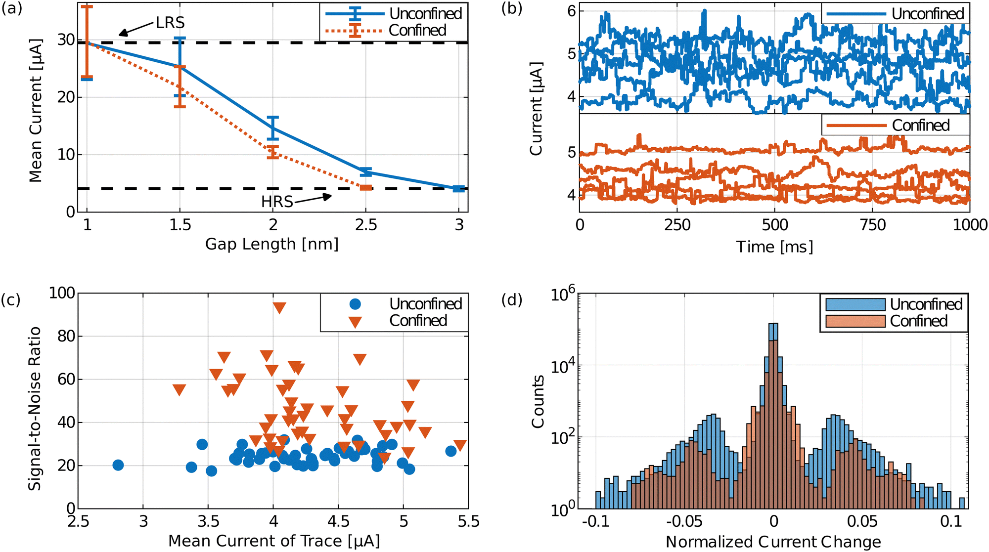 | ||
| Fig. 5 (a) Simulated current dependence on various gap lengths between filament and AE for a confined (orange) and an unconfined filament (blue). Both filaments are initially programmed in the same LRS (upper dashed line) and then investigated at a comparable HRS (lower dashed line). (b) Simulated current traces for five exemplary confined (orange) and unconfined filaments (blue). (c) SNR for 50 current traces of confined (orange) and unconfined (blue) filaments each. (d) Histogram of normalized current changes from one simulation time step to the next. The current changes are compared on a logarithmic scale for the confined (orange) and unconfined filament (blue). | ||
Dynamic simulations of the read variability of VCM cells are conducted using the 3D KMC model with the previously described filament properties. Thus, we applied a read voltage of 0.3 V at room temperature to the cell and detected the current evolution over time for 50 cells with confined and unconfined filaments, respectively. Fig. 5(b) depicts five exemplary current traces each, for a total simulated read duration of 1 s. In both cases, different current jump amplitudes are observed and they occur at various frequencies. The underlying cause is vacancy diffusion between different positions within the filament or gap. This noisy current behavior for the HRS accurately reproduces measured ionic noise as shown by Kopperberg et al.62 and is associated with the inherent randomness of the vacancy distribution and their movement induced by thermal or electrical activation. We report a decrease in the current noise for the confined filament (orange), showing less deviation from the mean current for the presented traces.
Fig. 5(c) depicts the SNR for all 50 simulated current traces of the confined and unconfined filaments, respectively. The SNR of the fully confined filaments (orange) exceed the unconfined reference filaments. This reinforces the previously measured SNR improvement for the partially confined filament in the nano-fin. However, the simulated fully confined filament shows increase of SNR for all observed cells. This indicates that two-dimensional confinement might result in a shift of the whole SNR distribution to higher values.
We clarify the underlying mechanisms of the observed reliability improvement by analyzing the vacancy diffusion instances and their respective impact on current changes (see Fig. 5(d)). In the simulation, each vacancy diffusion instance corresponds to one event-driven time step (Fig. S10, ESI†). We normalize the current changes between these consecutive time steps by the mean current of the trace. The comparison of current changes in confined and unconfined filaments from the logarithmic histogram reveal a comparable amount of small <2% current changes, whereas in the unconfined filament (blue) there is a multifold increase of vacancy diffusion instances causing higher current changes of >2%. Additionally, less frequent diffusion events with up to 10% current change in the unconfined filament are mitigated in the confined filament. It can be noted, that the simulated current change distribution is less continuous compared to the experimental results. This can be attributed to the cubic lattice of the model, which is a simplification of the more complex real structure of the oxide. Furthermore, in the KMC model, the oxygen vacancy jumps always take place consecutively without any timely overlap and thus without any superposed current changes.
Thus, we propose that filament confinement manipulates three filament properties, which are the underlying cause for the observed reliability improvements: higher oxygen vacancy concentration, lower absolute amount of oxygen vacancies and a smaller gap between filament and AE. Single vacancy diffusion events have less impact on the resistive state for filaments with higher oxygen vacancy concentration, as each individual diffusion affects the relative change in local vacancy concentration to a lesser degree. Notably, despite the higher vacancy concentration, the smaller confined filament has a lower absolute amount of oxygen vacancies contributing to noise through diffusive processes. Finally, the smaller gap in the confined filament reduces the impact of oxygen vacancy reconfiguration at the filament-gap interface on overall resistance change. This effectively shifts the filament properties further towards LRS-like behavior, which is known to directly relate to improved device performance with regard to noise57–61 and cycle-to-cycle resistance variability.10,63–65
Conclusions
We demonstrate successful fabrication of a nano-fin device that laterally confines the filament to 10 nm within an oxygen diffusion barrier material. While we observe improved HRS write-variability in our full factorial analysis of I–V sweeps, different peripheral device architectures can influence dynamic switching beyond filament confinement effects. Here, we use ionic noise measurements that are unaffected by these peripheral effects to show, that filament confinement can exhibit a multifold improvement in SNR. However, the noise behavior of the partially confined filament in the nano-fin is similar to unconfined reference devices in worst-case scenarios, which we attribute to filament fringe effects presumably along the unconfined dimension. We expect further noise improvement by fully confining the filament. Our complementing simulation reveals improved resistance state stability through increased oxygen vacancy concentration and a smaller gap between filament and active electrode compared to unconfined filaments with the same resistance state.The limiting nature of resistance fluctuation in filamentary oxide-based memristive devices, inherently linked to the randomness of vacancy (re-)distribution, remains a challenge. Nevertheless, our proposed device design can shift the HRS filament stability towards more reliable LRS-like behavior. Advancing from a pure electrode scaling to an oxide volume scaling approach could offer even more pronounced benefits on filament stability in retention measurements, where the detrimental impacts of diffusive processes are exacerbated.
Methods
Reference micro-devices
The reference devices with a thin film stack of Pt/Ta/TaOx/Pt are fabricated by optical lithography with lift-off method to make a micro-sized cross-bar structure. The sputter-deposited 6 μm wide and 50 nm thin Ta-bottom-electrode is thermally oxidized at the surface under dry oxygen atmosphere with various annealing temperatures and durations: Micro-device A at 300 °C for 10 min, micro-device B at 250 °C for 10 min, micro-device C at 300 °C for 2.5 min and micro-device D at 350 °C for 2.5 min. The resulting oxides are between 4–9 nm thin. Native oxide, as used in the nano-fin device, does not yield reliable switching for micro-sized devices. After surface oxidation, a 2 μm wide and 30 nm thin Pt top electrode is sputter-deposited on the reference devices.Measurement setup for full factorial analysis
Electrical measurements were performed using a fast current-limiting setup introduced by Hennen et al.66 The setup continuously collects full I–V traces at high speed and has two separate inputs for control waveforms; Va(t) sets the voltage to apply to the device and Vcc(t) sets the current limit for the negative (SET) polarity. We defined these waveforms to step through the Cartesian product of two control parameter ranges (50 linearly spaced values each) in raster fashion. Va(t) was composed of concatenated bipolar triangular sweeps, each with 1 ms period, ramping between a fixed minimum Vset,stop = − 1.8 V and a variable maximum Vreset,stop value. Vcc(t) was a piecewise constant signal with step transitions at selected (negatively sloped) zero crossings of the voltage control waveforms (Va = 0, ), which sets the variable current compliance values.
We programmed these waveforms for synchronized output from a Rigol DG5102 arbitrary waveform generator so that the matrix of 2500 control parameter combinations was probed in a single ten second measurement shot per device, with each condition revisited four times per shot. This measurement shot was repeated 10 times per device for a total of 100000 cycles for full factorial analysis.
Noise measurement
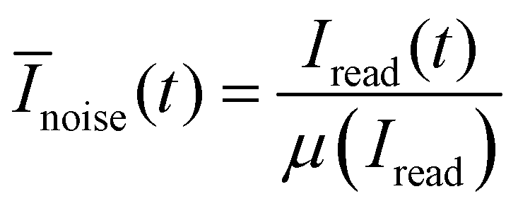
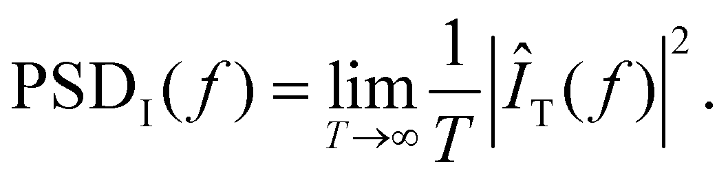
We monitored the read noise experiments with a Keithley 4200-SCS measurement setup using pulse measurement units (PMU) 4225 and remote pulse modules (RPM) 4225 from Keithley. The general idea of the two-step algorithm we used for this investigation follows Schnieders et al.56 First, the device is switched several times to check if the device is functional. If the on–off ratio exceeds a value of 5, the device is assumed to have switched. Subsequently, the state of the device is read by a constant voltage bias of 0.2 V applied to the AE for 2 seconds. We call the current response of this read pulse a trace. In this study we investigated traces in the HRS range of 20 kΩ to 200 kΩ. We define the signal-to-noise ratio (SNR) to compare the relative amplitude of noise signals as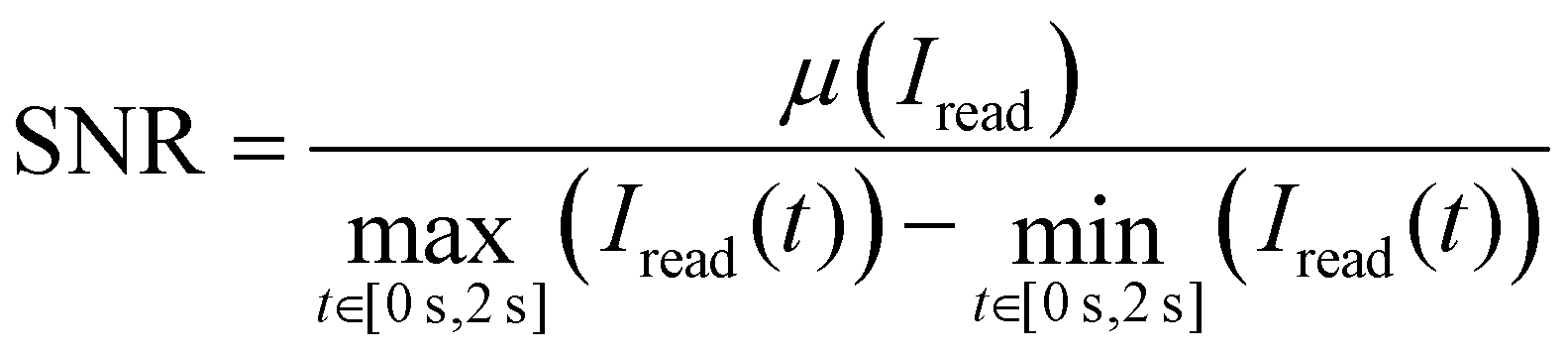 | (1) |
 | (2) |
| ΔĪδt,noise(t) = Īnoise(t) − Īnoise(t + δt). | (3) |
For this paper we chose δt = 120 μs. The power spectral density is calculated by
 | (4) |
 | (5) |
3D KMC simulation
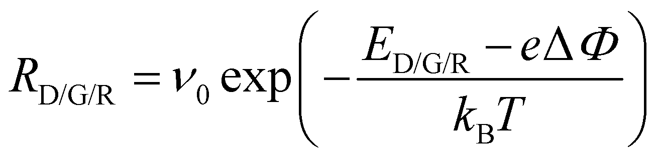
In this study we applied our 3D KMC simulation model with diffusion-limiting domains that was first presented by Kopperberg et al.62 The key advantage of this model, as opposed to other simulation models like compact models, is the ability to conduct statistical investigations of random processes.67 The simulation model is based on a cubic (6 nm)3 lattice structure with a distance of 0.5 nm between each lattice point, representing a HfOx-like layer sandwiched between two electrodes. Oxygen vacancies, that play a crucial role concerning the conduction in VCM devices, can be placed at the lattice points. Depending on the oxygen vacancy distribution and the externally applied voltage, the potential can be calculated via solving the Poisson's equation. For the calculation of the current, a trap-assisted-tunneling (TAT) solver is used, which is appropriate for the description of systems with comparably low oxygen vacancy concentrations as we expect it focusing on the HRS of our cells.68We used the 3D KMC model to simulate the variability in current traces. Here, the three possible transitions of generation, recombination, and diffusion of oxygen vacancy play an essential role as the rearrangement of oxygen vacancy has been detected as central process concerning read variability in VCM devices.62 Thus, transition rates can be calculated via
 | (6) |
Author contributions
P. S. conceived the concept, designed and fabricated devices, designed and carried out electrical measurements, analyzed data and wrote the manuscript. N. K. designed and carried out simulations, analyzed data and co-wrote the manuscript. K. S. designed and carried out electrical measurements, analyzed data and co-wrote the manuscript. T. H. designed and built experimental setup, designed measurement methodology and co-wrote the manuscript. S. W. validated and reviewed. S. M. validated and reviewed. R. W. supervised. D. J. W. supervised, validated and reviewed.Conflicts of interest
There are no conflicts to declare.Acknowledgements
This work was in part funded by the German Research Foundation (DFG) under grant no. SFB 917, in part by the Federal Ministry of Education and Research (BMBF, Germany) in the Projects NEUROTEC 2 (project no. 16ME0398K and 16ME0399) and NeuroSys (no. 03ZU1106AA and 03ZU1106BA), and is based on the Jülich Aachen Research Alliance (JARA-FIT). The authors gratefully acknowledge computing time on the supercomputer JURECA71 at Forschungszentrum Jülich under grant no. 27525 and the use of the clean room facility Helmholtz Nano Facility (HNF). We want to thank Dr Jhih-Sian Tu, Dr Thomas Grap, Lena Raffauf, Petra Grewe, Erdoglija Daliborka, Ekaterina Gorbunova and Thomas Pössinger for fruitful discussions and support.Notes and references
- D. S. Jeong, K. M. Kim, S. Kim, B. J. Choi and C. S. Hwang, Adv. Electron. Mater., 2016, 2, 1600090 CrossRef.
- M. Horowitz, 2014 IEEE International Solid-State Circuits Conference Digest of Technical Papers (ISSCC), 2014, pp. 10–14.
- A. Sebastian, M. Le Gallo, R. Khaddam-Aljameh and E. Eleftheriou, Nat. Nanotechnol., 2020, 15, 529–544 CrossRef CAS PubMed.
- J. Li, H. Abbas, D. S. Ang, A. Ali and X. Ju, Nanoscale Horiz., 2023, 8, 1456–1484 RSC.
- R. Dittmann, S. Menzel and R. Waser, Adv. Phys., 2021, 70, 155–349 CrossRef.
- Resistive switching: From fundamentals of nanoionic redox processes to memristive device applications, ed. D. Ielmini and R. Waser, Wiley-VCH, Weinheim, 2016 Search PubMed.
- R. Waser, R. Bruchhaus and S. Menzel, Nanoelectronics and information technology, Wiley-VCH, Weinheim, 2012, pp.683–710 Search PubMed.
- W. Wan, R. Kubendran, C. Schaefer, S. B. Eryilmaz, W. Zhang, D. Wu, S. Deiss, P. Raina, H. Qian, B. Gao, S. Joshi, H. Wu, H.-S. P. Wong and G. Cauwenberghs, Nature, 2022, 608, 504–512 CrossRef CAS PubMed.
- P. Yao, H. Wu, B. Gao, J. Tang, Q. Zhang, W. Zhang, J. J. Yang and H. Qian, Nature, 2020, 577, 641–646 CrossRef CAS PubMed.
- J. Doevenspeck, R. Degraeve, A. Fantini, S. Cosemans, A. Mallik, P. Debacker, D. Verkest, R. Lauwereins and W. Dehaene, IEEE Trans. Electron Devices, 2021, 68, 2301–2305 Search PubMed.
- Y. Xi, X. Li, J. Chen, R. Hu, Q. Zhang, Z. Jiang, F. Xu and J. Tang, 2023 IEEE International Reliability Physics Symposium (IRPS), 2023, pp. 1–7.
- V. Milo, C. Zambelli, P. Olivo, E. Pérez, M. K. Mahadevaiah, O. G. Ossorio, C. Wenger and D. Ielmini, APL Mater., 2019, 7, 081120 CrossRef.
- Z. Chai, P. Freitas, W. Zhang, F. Hatem, J. F. Zhang, J. Marsland, B. Govoreanu, L. Goux and G. S. Kar, IEEE Electron Device Lett., 2018, 39, 1652–1655 CAS.
- Y. Feng, P. Huang, Y. Zhao, Y. Shan, Y. Zhang, Z. Zhou, L. Liu, X. Liu and J. Kang, IEEE Electron Device Lett., 2021, 42, 1168–1171 CAS.
- M. Zhao, H. Wu, B. Gao, Q. Zhang, W. Wu, S. Wang, Y. Xi, D. Wu, N. Deng, S. Yu, H.-Y. Chen and H. Qian, IEDM: 2017 IEEE International Electron Devices Meeting: 2-6 December 2017, 12/2/2017 – 12/6/2017, pp. 39.4.1–39.4.4.
- M. Zhao, B. Gao, J. Tang, H. Qian and H. Wu, Appl. Phys. Rev., 2020, 7, 011301 CAS.
- C. Baeumer, C. Schmitz, A. Marchewka, D. N. Mueller, R. Valenta, J. Hackl, N. Raab, S. P. Rogers, M. I. Khan, S. Nemsak, M. Shim, S. Menzel, C. M. Schneider, R. Waser and R. Dittmann, Nat. Commun., 2016, 7, 12398 CrossRef CAS PubMed.
- C. Baeumer, R. Valenta, C. Schmitz, A. Locatelli, T. O. Mentes, S. P. Rogers, A. Sala, N. Raab, S. Nemsak, M. Shim, C. M. Schneider, S. Menzel, R. Waser and R. Dittmann, ACS Nano, 2017, 11, 6921–6929 CrossRef CAS PubMed.
- T. Heisig, K. Lange, A. Gutsche, K. T. Goß, S. Hambsch, A. Locatelli, T. O. Mentes, F. Genuzio, S. Menzel and R. Dittmann, Adv. Electron. Mater., 2022, 8, 2100936 CrossRef CAS.
- S. Kumar, Z. Wang, X. Huang, N. Kumari, N. Davila, J. P. Strachan, D. Vine, A. L. D. Kilcoyne, Y. Nishi and R. S. Williams, ACS Nano, 2016, 10, 11205–11210 CrossRef CAS PubMed.
- J. P. Strachan, M. D. Pickett, J. J. Yang, S. Aloni, A. L. David Kilcoyne, G. Medeiros-Ribeiro and R. Stanley Williams, Adv. Mater., 2010, 22, 3573–3577 CrossRef CAS PubMed.
- F. Miao, J. P. Strachan, J. J. Yang, M.-X. Zhang, I. Goldfarb, A. C. Torrezan, P. Eschbach, R. D. Kelley, G. Medeiros-Ribeiro and R. S. Williams, Adv. Mater., 2011, 23, 5633–5640 CrossRef CAS PubMed.
- U. Celano, J. Op de Beeck, S. Clima, M. Luebben, P. M. Koenraad, L. Goux, I. Valov and W. Vandervorst, ACS Appl. Mater. Interfaces, 2017, 9, 10820–10824 CrossRef CAS PubMed.
- U. Celano, Y. Yin Chen, D. J. Wouters, G. Groeseneken, M. Jurczak and W. Vandervorst, Appl. Phys. Lett., 2013, 102, 121602 CrossRef.
- M. Rao, H. Tang, J. Wu, W. Song, M. Zhang, W. Yin, Y. Zhuo, F. Kiani, B. Chen, X. Jiang, H. Liu, H.-Y. Chen, R. Midya, F. Ye, H. Jiang, Z. Wang, M. Wu, M. Hu, H. Wang, Q. Xia, N. Ge, J. Li and J. J. Yang, Nature, 2023, 615, 823–829 CrossRef CAS PubMed.
- D.-H. Kwon, K. M. Kim, J. H. Jang, J. M. Jeon, M. H. Lee, G. H. Kim, X.-S. Li, G.-S. Park, B. Lee, S. Han, M. Kim and C. S. Hwang, Nat. Nanotechnol., 2010, 5, 148–153 CrossRef CAS PubMed.
- D.-H. Kwon, S. Lee, C. S. Kang, Y. S. Choi, S. J. Kang, H. L. Cho, W. Sohn, J. Jo, S.-Y. Lee, K. H. Oh, T. W. Noh, R. A. de Souza, M. Martin and M. Kim, Adv. Mater., 2019, 31, e1901322 CrossRef PubMed.
- H. Du, C.-L. Jia, A. Koehl, J. Barthel, R. Dittmann, R. Waser and J. Mayer, Chem. Mater., 2017, 29, 3164–3173 CrossRef CAS.
- Z. Wei and K. Eriguchi, IEEE Trans. Electron Devices, 2017, 64, 2201–2206 CAS.
- Y. Hayakawa, A. Himeno, R. Yasuhara, W. Boullart, E. Vecchio, T. Vandeweyer, T. Witters, D. Crotti, M. Jurczak, S. Fujii, S. Ito, Y. Kawashima, Y. Ikeda, A. Kawahara, K. Kawai, Z. Wei, S. Muraoka, K. Shimakawa, T. Mikawa and S. Yoneda, 2015 Symposium on VLSI Technology (VLSI Technology), 2015, pp. T14–T15.
- Z. Wei, T. Takagi, Y. Kanzawa, Y. Katoh, T. Ninomiya, K. Kawai, S. Muraoka, S. Mitani, K. Katayama, S. Fujii, R. Miyanaga, Y. Kawashima, T. Mikawa, K. Shimakawa and K. Aono, 2011 International Electron Devices Meeting, 2011, pp. 31.4.1–31.4.4.
- Y. Ma, D. Li, A. A. Herzing, D. A. Cullen, B. T. Sneed, K. L. More, N. T. Nuhfer, J. A. Bain and M. Skowronski, ACS Appl. Mater. Interfaces, 2018, 10, 23187–23197 CrossRef CAS PubMed.
- S. Gao, G. Liu, Q. Chen, W. Xue, H. Yang, J. Shang, B. Chen, F. Zeng, C. Song, F. Pan and R.-W. Li, ACS Appl. Mater. Interfaces, 2018, 10, 6453–6462 CrossRef CAS PubMed.
- J. Meng, B. Zhao, Q. Xu, J. M. Goodwill, J. A. Bain and M. Skowronski, J. Appl. Phys., 2020, 127, 235107 CrossRef CAS.
- X. Sheng, C. E. Graves, S. Kumar, X. Li, B. Buchanan, L. Zheng, S. Lam, C. Li and J. P. Strachan, Adv. Electron. Mater., 2019, 5, 1800876 CrossRef.
- M.-J. Lee, C. B. Lee, D. Lee, S. R. Lee, M. Chang, J. H. Hur, Y.-B. Kim, C.-J. Kim, D. H. Seo, S. Seo, U.-I. Chung, I.-K. Yoo and K. Kim, Nat. Mater., 2011, 10, 625–630 CrossRef CAS PubMed.
- Y. Y. Chen, R. Degraeve, S. Clima, B. Govoreanu, L. Goux, A. Fantini, G. S. Kar, G. Pourtois, G. Groeseneken, D. J. Wouters and M. Jurczak, 2012 International Electron Devices Meeting, 2012, pp. 20.3.1–20.3.4.
- C. Y. Chen, L. Goux, A. Fantini, A. Redolfi, S. Clima, R. Degraeve, Y. Y. Chen, G. Groeseneken and M. Jurczak, 2014 IEEE International Electron Devices Meeting, 2014, pp. 14.2.1–14.2.4.
- B. Govoreanu, S. Kubicek, G. Kar, Y. Y. Chen, V. Paraschiv, M. Rakowski, R. Degraeve, L. Goux, S. Clima, N. Jossart, C. Adelmann, O. Richard, T. Raes, D. Vangoidsenhoven, T. Vandeweyer, H. Tielens, K. Kellens, K. Devriendt, N. Heylen, S. Brus, B. Verbrugge, L. Pantisano, H. Bender, G. Pourtois, J. A. Kittl, D. J. Wouters, L. Altimime and M. Jurczak, Extended Abstracts of the 2011 International Conference on Solid State Devices and Materials, 2011.
- J. Niu, M. Zhang, Y. Li, S. Long, H. Lv, Q. Liu and M. Liu, J. Vac. Sci. Technol., B: Nanotechnol. Microelectron.: Mater., Process., Meas., Phenom.a, 2016, 34, 02G105 Search PubMed.
- W. C. Chien, Y. R. Chen, Y. C. Chen, A. T. Chuang, F. M. Lee, Y. Y. Lin, E. K. Lai, Y. H. Shih, K. Y. Hsieh and C.-Y. Lu, 2010 International Electron Devices Meeting, 2010, pp. 19.2.1–19.2.4.
- W.-C. Chien, M.-H. Lee, F.-M. Lee, Y.-Y. Lin, H.-L. Lung, K.-Y. Hsieh and C.-Y. Lu, 2011 International Electron Devices Meeting, 2011, pp. 31.5.1–31.5.4.
- M.-C. Hsieh, Y.-C. Liao, Y.-W. Chin, C.-H. Lien, T.-S. Chang, Y.-D. Chih, S. Natarajan, M.-J. Tsai, Y.-C. King and C. J. Lin, 2013 IEEE International Electron Devices Meeting, 2013, pp. 10.3.1–10.3.4.
- O. Golonzka, U. Arslan, P. Bai, M. Bohr, O. Baykan, Y. Chang, A. Chaudhari, A. Chen, J. Clarke, C. Connor, N. Das, C. English, T. Ghani, F. Hamzaoglu, P. Hentges, P. Jain, C. Jezewski, I. Karpov, H. Kothari, R. Kotlyar, B. Lin, M. Metz, J. Odonnell, D. Ouellette, J. Park, A. Pirkle, P. Quintero, D. Seghete, M. Sekhar, A. S. Gupta, M. Seth, N. Strutt, C. Wiegand, H. J. Yoo and K. Fischer, 2019 Symposium on VLSI Technology, 2019, pp. T230–T231.
- B. Govoreanu, G. S. Kar, Y.-Y. Chen, V. Paraschiv, S. Kubicek, A. Fantini, I. P. Radu, L. Goux, S. Clima, R. Degraeve, N. Jossart, O. Richard, T. Vandeweyer, K. Seo, P. Hendrickx, G. Pourtois, H. Bender, L. Altimime, D. J. Wouters, J. A. Kittl and M. Jurczak, 2011 International Electron Devices Meeting, 2011, pp. 31.6.1–31.6.4.
- G. S. Kar, A. Fantini, Y.-Y. Chen, V. Paraschiv, B. Govoreanu, H. Hody, N. Jossart, H. Tielens, S. Brus, O. Richard, T. Vandeweyer, D. J. Wouters, L. Altimime and M. Jurczak, 2012 Symposium on VLSI Technology (VLSIT), 2012, pp. 157–158.
- K.-S. Li, C. Ho, M.-T. Lee, M.-C. Chen, C.-L. Hsu, J. M. Lu, C. H. Lin, C. C. Chen, B. W. Wu, Y. F. Hou, C. Y. Lin, Y. J. Chen, T. Y. Lai, M. Y. Li, I. Yang, C. S. Wu and F.-L. Yang, 2014 Symposium on VLSI Technology (VLSI-Technology): Digest of Technical Papers, 2014, pp. 1–2.
- S. Pi, C. Li, H. Jiang, W. Xia, H. Xin, J. J. Yang and Q. Xia, Nat. Nanotechnol., 2019, 14, 35–39 CrossRef CAS PubMed.
- E. Cha, J. Woo, D. Lee, S. Lee, J. Song, Y. Koo, J. Lee, C. G. Park, M. Y. Yang, K. Kamiya, K. Shiraishi, B. Magyari-Kope, Y. Nishi and H. Hwang, 2013 IEEE International Electron Devices Meeting, 2013, pp. 10.5.1–10.5.4.
- M. Yu, Y. Cai, Z. Wang, Y. Fang, Y. Liu, Z. Yu, Y. Pan, Z. Zhang, J. Tan, X. Yang, M. Li and R. Huang, Sci. Rep., 2016, 6, 21020 CrossRef CAS PubMed.
- H.-Y. Chen, S. Yu, B. Gao, R. Liu, Z. Jiang, Y. Deng, B. Chen, J. Kang and H.-S. P. Wong, Nanotechnology, 2013, 24, 465201 CrossRef PubMed.
- T. Enomoto, R. Ando, H. Morita and H. Nakayama, Jpn. J. Appl. Phys., 1978, 17, 1049–1058 CrossRef CAS.
- T. Hennen, E. Wichmann, R. Waser, D. J. Wouters and D. Bedau, Rev. Sci. Instrum., 2022, 93, 024705 CrossRef CAS PubMed.
- S. Wiefels, C. Bengel, N. Kopperberg, K. Zhang, R. Waser and S. Menzel, IEEE Trans. Electron Devices, 2020, 67, 4208–4215 CAS.
- Y. Pan, Y. Cai, Y. Liu, Y. Fang, M. Yu, S. Tan and R. Huang, Appl. Phys. Lett., 2016, 108, 153504 CrossRef.
- K. Schnieders, C. Funck, F. Cüppers, S. Aussen, T. Kempen, A. Sarantopoulos, R. Dittmann, S. Menzel, V. Rana, S. Hoffmann-Eifert and S. Wiefels, APL Mater., 2022, 10, 101114 CrossRef CAS.
- S. Yu, R. Jeyasingh, Y. Wu and H.-S. P. Wong, Phys. Rev. B: Condens. Matter Mater. Phys., 2012, 85, 045324 CrossRef.
- F. M. Puglisi, N. Zagni, L. Larcher and P. Pavan, IEEE Trans. Electron Devices, 2018, 65, 2964–2972 CAS.
- B. Sánta, Z. Balogh, L. Pósa, D. Krisztián, T. N. Török, D. Molnár, C. Sinkó, R. Hauert, M. Csontos and A. Halbritter, ACS Appl. Mater. Interfaces, 2021, 13, 7453–7460 CrossRef PubMed.
- D. Ielmini, S. Ambrogio and S. Balatti, ECS Trans., 2013, 58, 165–173 CrossRef.
- J. Lee, J. Shin, D. Lee, W. Lee, S. Jung, M. Jo, J. Park, K. P. Biju, S. Kim, S. Park and H. Hwang, 2010 International Electron Devices Meeting, 2010, pp. 19.5.1–19.5.4.
- N. Kopperberg, S. Wiefels, S. Liberda, R. Waser and S. Menzel, ACS Appl. Mater. Interfaces, 2021, 13, 58066–58075 CrossRef CAS PubMed.
- A. Fantini, L. Goux, R. Degraeve, D. J. Wouters, N. Raghavan, G. Kar, A. Belmonte, Y.-Y. Chen, B. Govoreanu and M. Jurczak, 2013 5th IEEE International Memory Workshop, 2013, pp. 30–33.
- I. Salaoru, A. Khiat, Q. Li, R. Berdan, C. Papavassiliou and T. Prodromakis, J. Phys. D: Appl. Phys., 2014, 47, 145102 CrossRef.
- X. Lian, X. Cartoixà, E. Miranda, L. Perniola, R. Rurali, S. Long, M. Liu and J. Suñé, J. Appl. Phys., 2014, 115, 244507 CrossRef.
- T. Hennen, E. Wichmann, A. Elias, J. Lille, O. Mosendz, R. Waser, D. J. Wouters and D. Bedau, Rev. Sci. Instrum., 2021, 92, 1274 CrossRef PubMed.
- S. Wiefels, N. Kopperberg, K. Hofmann, J. Otterstedt, D. Wouters, R. Waser and S. Menzel, pssa - Special Issue - accepted, 2023, xx, xxxx.
- L. Larcher, IEEE Trans. Electron Devices, 2003, 50, 1246–1253 CrossRef CAS.
- E. Abbaspour, S. Menzel, A. Hardtdegen, S. Hoffmann-Eifert and C. Jungemann, IEEE Trans. Nanotechnol., 2018, 17, 1181–1188 CAS.
- S. Aldana, J. B. Roldán, P. García-Fernández, J. Suñe, R. Romero-Zaliz, F. Jiménez-Molinos, S. Long, F. Gómez-Campos and M. Liu, J. Appl. Phys., 2018, 123, 154501 CrossRef.
- Jülich Supercomputing Centre, J. Large-Scale Res. Facili., 2021, 7, A182 CrossRef.
Footnotes |
| † Electronic supplementary information (ESI) available. See DOI: https://doi.org/10.1039/d3nh00520h |
| ‡ These authors contributed equally to this work. |
| This journal is © The Royal Society of Chemistry 2024 |