
Oxide and 2D TMD semiconductors for 3D DRAM cell transistors
Jae Seok
Hur†
 a,
Sungsoo
Lee†
b,
Jiwon
Moon
b,
Hang-Gyo
Jung
c,
Jongwook
Jeon
b,
Seong Hun
Yoon
e,
Jin-Hong
Park
*bd and
Jae Kyeong
Jeong
*ae
a,
Sungsoo
Lee†
b,
Jiwon
Moon
b,
Hang-Gyo
Jung
c,
Jongwook
Jeon
b,
Seong Hun
Yoon
e,
Jin-Hong
Park
*bd and
Jae Kyeong
Jeong
*ae
aDepartment of Electronic Engineering, Hanyang University, Seoul 04763, Republic of Korea. E-mail: jkjeong1@hanyang.ac.kr
bDepartment of Electrical and Computer Engineering, Sungkyunkwan University, Suwon 16419, Republic of Korea. E-mail: jhpark9@skku.edu
cDepartment of Semiconductor Convergence Engineering, Sungkyunkwan University, Suwon 16419, Republic of Korea
dAdvanced Institute of Nano Technology (SAINT), Sungkyunkwan University, Suwon 16419, Republic of Korea
eDepartment of Display Science and Engineering, Hanyang University, Seoul 04763, Republic of Korea
First published on 25th March 2024
Abstract
As the downscaling of conventional dynamic random-access memory (DRAM) has reached its limits, 3D DRAM has been proposed as a next-generation DRAM cell architecture. However, incorporating silicon into 3D DRAM technology faces various challenges in securing cost-effective high cell transistor performance. Therefore, many researchers are exploring the application of next-generation semiconductor materials, such as transition oxide semiconductors (OSs) and metal dichalcogenides (TMDs), to address these challenges and to realize 3D DRAM. This study provides an overview of the proposed structures for 3D DRAM, compares the characteristics of OSs and TMDs, and discusses the feasibility of employing the OSs and TMDs as the channel material for 3D DRAM. Furthermore, we review recent progress in 3D DRAM using the OSs, discussing their potential to overcome challenges in silicon-based approaches.
 Jae Seok Hur | Jae Seok Hur received a BS degree from Kyunghee University, South Korea, majoring in Information Displays in 2016. Subsequently, he received a MS degree from Hanyang University, South Korea, majoring in Information Display Engineering in 2019. Currently, he is studying toward a PhD degree at the Department of Electronic Engineering at Hanyang University. His research interests include n-type oxide semiconductor materials and devices based on atomic layer deposition, as well as emerging thin-film transistor technologies and their applications. |
 Sungsoo Lee | Sungsoo Lee received a BS degree in Advanced Materials Science from Sungkyunkwan University in 2022. He is currently working toward an M.S. degree at the Department of Electrical and Computer Engineering at Sungkyunkwan University. His current research interests focus on DRAM cell transistors based on 2D vdW materials and oxide semiconductor materials. |
 Jiwon Moon | Jiwon Moon received a BS degree in Electronic Engineering from Kyunghee University, Seoul, South Korea, in 2018. She is currently working toward an Integrated MS and PhD degree at the Department of Electrical and Computer Engineering at Sungkyunkwan University. Her research focuses on next-generation devices utilizing 2D TMD semiconductors, 3D DRAM cell transistors, and their applications. |
 Hang-Gyo Jung | Hang-gyo Jung received his BS degree in Physics and MS degree in Electrical and Electronic Engineering from Konkuk University in Seoul, South Korea. Currently, he is pursuing his PhD at Sungkyunkwan University in Suwon, South Korea. His research interests lie in the simulation of next-generation semiconductor devices, compact modeling, and design-technology co-optimization (DTCO). |
 Jongwook Jeon | Jongwook Jeon received a BS degree in Electrical Engineering from Sungkyunkwan University, in 2004, and the PhD degree in Electrical Engineering from Seoul National University, Seoul, South Korea, in 2009. He was a Senior Engineer and a Principal Engineer with the Samsung Research and Development Center, South Korea, from 2009 to 2017. From 2017 to 2023, he was an assistant and associate professor at Konkuk University, Seoul, South Korea. Since 2023, he has been an associate professor in the Department of Electrical and Computer Engineering at Sungkyunkwan University, Suwon, South Korea, focusing on design-technology co-optimization (DTCO) for next-generation semiconductor technology. |
 Seong Hun Yoon | Seong Hun Yoon received a BS and MS degree from the Department of Electronic Engineering at Hanyang University, South Korea, in 2021 and 2023, respectively. He is currently working toward a PhD degree at the Department of Display Science and Engineering at Hanyang University. His research interests include semiconductor/insulating oxide materials and devices based on atomic layer deposition for emerging display/memory applications. |
 Jin-Hong Park | Jin-Hong Park holds the title of Distinguished Professor (SKKU Fellow) at Sungkyunkwan University (SKKU) in South Korea, where he is affiliated with the Department of Electrical and Computer Engineering, Department of Semiconductor Convergence Engineering, Sungkyunkwan Advanced Institute of Nanotechnology (SAINT). Prof. Park earned his MS and PhD degrees in electrical engineering from Stanford University in the United States in 2009. He furthered his academic and research career as a postdoctoral researcher at the IBM Thomas J. Watson Research Center from 2009 to 2010. Following his postdoctoral work, Prof. Park served as an Assistant Professor at Kyung Hee University from 2010 to 2011. He subsequently joined Sungkyunkwan University (SKKU) and has worked as an Assistant, Associate, and Full Professor. Prof. Park also contributes to the field of nanoscale research as an Editorial Board Member of Nanoscale Horizons, The Royal Society of Chemistry. His research interests primarily include developing advanced low-power devices utilizing 2D van der Waals (vdW) materials, such as gate-all-around FETs, multivalued logic devices, and neuromorphic devices. Additionally, he focuses on the fabrication technologies related to 2D vdW materials and oxide–semiconductor materials. |
 Jae Kyeong Jeong | Jae Kyeong Jeong received his BS, MS, and PhD degrees in Material Science and Engineering from Seoul National University, Seoul, Korea, in 1997, 1999, and 2002, respectively. In 2003, he served as a post-doctoral researcher at the University of Illinois at Urbana–Champaign in the United States. He then joined Samsung Display Corp. as a senior engineer in 2004, focusing on research related to the design and characterization of LTPS and IGZO TFTs for AMOLED display. Notably, as a project leader at Samsung Display, he led groundbreaking research in oxide TFTs, culminating in the unveiling of the world's largest 12.1′′ Oxide TFT-driven AMOLED display in 2008. In 2009, he transitioned to academia, joining Inha University at an assistant professor. Since 2015, he has served as a Professor in the Department of Electronic Engineering at Hanyang University, Seoul, Republic of Korea. His research has expanded to encompass novel devices such as oxide TFTs, flexible electronics, CMOS TFTs, and memory technologies. With over 198 SCI journal papers and 120 international patents, he holds an H-index of 63 and over 25 |
![[thin space (1/6-em)]](https://www.rsc.org/images/entities/char_2009.gif) 000 citations according to Google Scholar. He became a member of the National Academy of Engineering of Korea (NAEK) in 2021 and currently serves on the editorial boards of Scientific Reports. Throughout his career, Jeong has received numerous awards, including the Merck Grand Award (2023) and the Distinguished Paper Award from SID (2008).
000 citations according to Google Scholar. He became a member of the National Academy of Engineering of Korea (NAEK) in 2021 and currently serves on the editorial boards of Scientific Reports. Throughout his career, Jeong has received numerous awards, including the Merck Grand Award (2023) and the Distinguished Paper Award from SID (2008).A. Introduction
In the era of big data, there has been a rapid increase in the volume of data handled by computers. The worldwide data generated in 2022 is projected to reach approximately 101 zettabytes, an annual growth rate of roughly 20%.1 The processing bottlenecks arising from this substantial increase in data volume are a primary challenge, and it is crucial to enhance the performance of dynamic random access memory (DRAM), a key component serving as the primary memory in contemporary computers.Enhancements in DRAM performance have been achieved through reductions in feature size and structural modifications. However, as feature sizes decreased beyond the 10 nm process node, leakage current has become the foremost challenge.2 The reduction in gate length leads to increased gate-induced drain leakage (GIDL), junction leakage, and channel leakage current, making it difficult to meet the desired refresh time targets.3 Scaling cell geometry has also encountered limitations. The current mass production employs the 6F2 architecture, while endeavors are underway to implement the 4F2 architecture through the introduction of vertical channel array transistors (VCAT). The 4F2 architecture, featuring one DRAM cell at each intersection of the word and bit lines, represents the most compact cell architecture achievable in a 2D structure. Scaling beyond 4F2 requires breakthroughs. Currently, active research is addressing physical limitations and seeking to diminish feature size through the incorporation of alternative channel materials. These materials must exhibit immunity to the short-channel effect while experiencing minimal degradation in ultra-thin body structures. Notable candidates include OSs and TMDs.4–7 The adoption of such materials facilitates the facile reduction of feature size, leading to significant improvements in DRAM performance, including operation speed and power consumption. In terms of cell geometry scaling, efforts are underway to introduce a vertically stacked DRAM, commonly referred to as “3D DRAM,” with a goal of higher integration compared to the 4F2 cell architecture. Numerous structures have been proposed, inducing ongoing discussions regarding the most suitable configuration. The novel channel materials present a promising pathway for development of 3D DRAM. Silicon technology faces challenges in implementing ultra-thin body structures, scaling feature size, minimizing GIDL, and reducing processing temperature, making it difficult to realize stacked 3D DRAM with dozens of layers. Numerous research efforts are currently in progress to tackle these physical obstacles through the utilization of advanced channel materials. Representative examples include oxide semiconductors (OSs) and transition metal dichalcogenides (TMDs). Their inherent characteristics, facilitating reduced process temperatures, enhanced scalability, and decreased leakage currents compared to silicon, position them as prospective channel options for 3D DRAM cell transistors.8,9
This review is organized as follows. In Part B, we provide a comprehensive overview of the evolution of DRAM cell structures. We compare the structures of 3D DRAM presented in patents and papers, along with their characteristics, from a process perspective. In Part C, we compare the features of OSs and TMDs from the perspective presented in Part B and discuss which materials may exhibit better performance when applied as channel material for the 3D DRAM cell array transistor. In Part D, we compare the critical issues that need addressing for the implementation of OSs and TMDs in 3D DRAM. We also review recent preliminary work related to OS-based DRAM cells.
B. Overview of DRAM cell structure
1. Evolution of DRAM cell structure
 | ||
| Fig. 1 Schematic diagrams of 3D DRAM proposed by (a) Samsung, (b) Hynix, and (c) Micron.14–16 Schematic diagrams of 3D DRAM with (d) vertical and (e) horizontal word lines.17 | ||
Compared to the horizontal capacitor, the vertical capacitor occupies a lower chip footprint (Fig. 1a). However, the process difficulty is high due to the formation of a high aspect ratio structure. The horizontal capacitor mitigates the process complexity, not requiring the formation of a vertical structure (Fig. 1b and c). However, enough layers should be stacked to compensate for the increased area of the larger chip footprint. To further increase integration density, the structure with the horizontal capacitor requires improvement in stacking technology, while the structure with the vertical capacitor requires enhancements in scaling techniques in the lateral direction. In cases where the horizontal capacitor and transistors are interconnected, two structures can be implemented depending on the orientation of the word line and bit line (Fig. 1d and e). In the scenario where the word line assumes a vertical orientation (as depicted in Fig. 1d), the lateral spacing between cells becomes wider, resulting in a larger footprint. However, this structure is predicted to have a lower height due to the reduced distance between layers. Conversely, when the word line takes a horizontal alignment (as depicted in Fig. 1e), the lateral spacing between cells decreases, reducing the overall cell area. However, this structure has a larger space between layers, resulting in a higher structure. Furthermore, the fabrication of horizontal word lines between cells adds complexity to the fabrication process flow.17,18
Furthermore, the deposition method and process temperature become crucial considerations when incorporating new channel semiconductor materials for the 3D DRAM cell array transistor. Physical vapor deposition (PVD) methods like sputtering exhibit inadequate step coverage and low uniformity, rendering them unsuitable for the 3D DRAM process. On the other hand, chemical vapor deposition (CVD) methods offer superior step coverage compared to PVD. However, achieving a high-quality thin film requires high temperatures in CVD, presenting a challenge in monolithic process integration schemes. The high process temperatures can lead to thermal budget issues, causing variations in the characteristics of upper and lower devices. Atomic layer deposition (ALD) stands out among CVD techniques due to its exceptional step coverage and uniformity, allowing the deposition of extremely thin and high-quality film. Nonetheless, the drawback of ALD is the necessity for the development of precursors tailored to the target materials.
Recently, OSs such as IGZO and TMDs like MoS2 have been proposed as next-generation semiconductor channel materials. OSs exhibit low off-current characteristics and are easy to mass-produce, allowing wide use in the display field. TMDs, with a thickness of sub-1 nm and high mobility characteristics, are also considered promising materials for next-generation semiconductor channel materials. In part C, we will compare the features of OSs and TMDs from the perspective presented in part B and discuss the performances predicted when they are applied to 3D DRAM cell array transistors.
C. Emerging channel materials and their device characteristics
1. Oxide semiconductors and TMD semiconductors
2. Transistor on/off characteristics
| Property | Channel materials | |||
|---|---|---|---|---|
| c-Si | 2D TMDs | Oxide semiconductors | ||
| Contact related | Contact resistance | 20–50 Ω μm | >1000 Ω μm | 500–2000 Ω μm |
| Barrier height (EF pinning) | ∼500 meV | ∼200 meV | 300–1000 meV (SBH) | |
| Doping concentration | 1021–1022 cm−3 | 1012–1013 cm−2 (1019–1020 cm−3 at d = 100 nm) | 1016–1018 cm−3 | |
| M–S gap | Negligible | 0.3–0.5 nm | Negligible | |
| Channel conductivity | Effective DOS | 3 × 1019 cm−3 | ∼1022 cm−3 | 5 × 1018 cm−3 |
| Mobility | ∼125 cm2 V−1 s−1 | 20–50 cm2 V−1 s−1 | 20–100 cm2 V−1 s−1 | |
| D it (with high-κ) | ∼1010 cm−2 eV−1 | ∼1013 cm−2 eV−1 | ∼1012 cm−2 eV−1 | |
| Property | Channel materials | |||
|---|---|---|---|---|
| c-Si | 2D TMDs | Oxide semiconductors | ||
| GIDL | Bandgap | 1.12 eV | 1.6 eV | >3.0 eV |
| D it (with high-κ) | ∼1010 cm−2 eV−1 | ∼1013 cm−2 eV−1 | ∼1012 cm−2 eV−1 | |
| Subthreshold leakage | ||||
| Thickness | ∼6 nm | <1 nm | 10–50 nm | |
| Junction leakage | Barrier height | PN junction (Eg – 500–1000) meV | Schottky junction (Eg – 1400) meV | Schottky junction (Eg – 300–1000) meV |
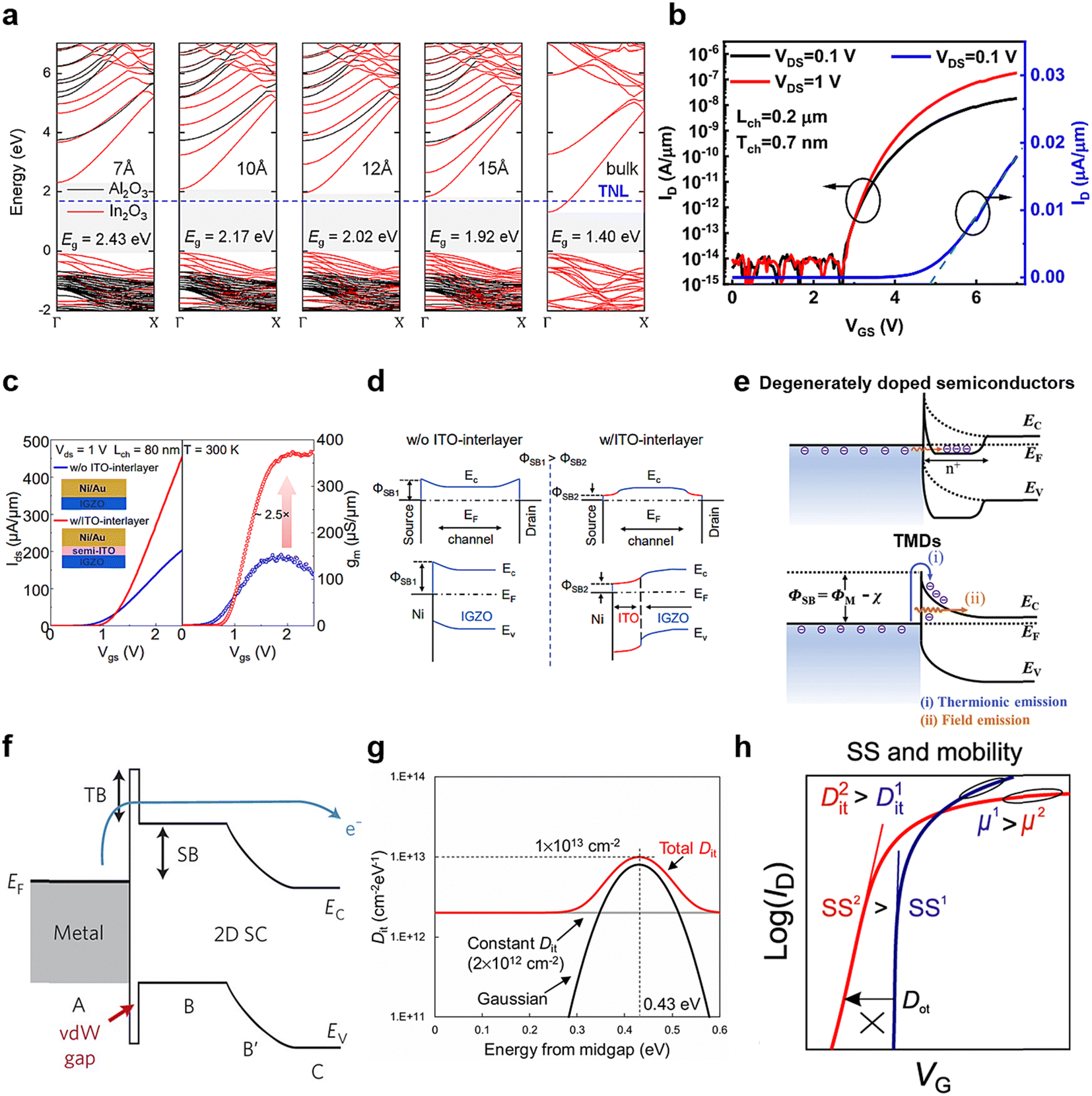 | ||
| Fig. 2 (a) DFT-calculated band structure at In2O3 film thicknesses of 0.7, 1.0, 1.2, and 1.5 nm and bulk along the Γ to X-direction, the red and black lines indicate the bands from In2O3 and Al2O3, respectively.38 (b) ID–VGS characteristics of In2O3 transistors with channel thickness of 0.7 nm.38 (c) IDS–VGS curves and extracted gm–VGS curves for a-IGZO TFTs with and without an ITO interlayer between M/S contact and (d) schematic band diagrams of SBH lowering with ITO interlayer.44 (e) Carrier injection characteristics in degenerately doped semiconductors and TMDs.53 (f) Band diagram of the metal–TMD interface with a van der Waals gap.55 (g) Dit distribution-extracted technology computer-aided design (TCAD) simulation at the MoS2–insulator interface.58 (h) Transfer characteristics as a function of Dit.59 | ||
Nevertheless, most OS FETs exhibit contact-limited behavior attributed to a notably high specific contact resistivity. Evidently, the diminishing contact area within nanoscale DRAM cells imposes a substantial constraint on the on-current, a phenomenon underscored in literature.43 In display backplane technologies where contact areas typically span a few μm2, the manageable nature of metal–OS contact resistance prevails even at levels of ∼104 Ω μm. However, within the intricate structure of DRAM cell transistors, the negative impact of contact resistance will be amplified, particularly in the context of 3D DRAM technology where contact areas may decrease to the ∼100 nm2 scale. Approaches to reduce contact resistance in OS FETs involve the insertion of suitable interlayers (ILs) or/and the formation of highly-doped n+ layers.44–46 Li et al. inserted ITO IL between IGZO and Ni contacts to achieve substantial enhancement of on-current (1207 μA μm−1) due to a reduction in contact resistance to 278 Ω μm (at 4.3 K) (Fig. 2c and d).44
Several reports have demonstrated TMD-based FETs in achieving on-currents surpassing 450 μA μm−1, due to their inherently excellent conductivity characteristics. These values align closely with the specifications outlined in the International Roadmap for Devices and Systems (IRDS) 2022.47–49 Consequently, TMDs can be utilized for DRAM cell transistors with exceptionally rapid write speeds or for peripheral transistors requiring specifications comparable to high-performance logic devices. Simulation-based studies on TMD FETs suggest that they have the potential to outperform silicon-based MOSFETs in terms of on-current, provided certain challenges are addressed.50,51 One such challenge is the high contact resistance; typical metal-TMD junctions exhibit contact resistance in the kiloohm range, which is several times higher than that of silicon–metal junctions. Although the metal-TMD Schottky barrier height is approximately 200 meV in the case of MoS2, a representative n-channel TMD material, this junction is expected to have a lower carrier injection rate than silicon–metal junctions due to the absence of an established degenerate doping technique (Fig. 2e).52,53 Moreover, there is a gap of approximately 0.3–0.5 nm at the metal–TMD interface, serving as an additional tunnelling barrier that impedes carrier injection (see Fig. 2f).54,55 This combination of low doping level and an interface gap contributes to the high contact resistance observed in TMD–metal junctions, prompting ongoing research efforts to address these challenges. Notably, Li et al. achieved a substantial reduction in contact resistance to 42 Ω μm by employing a semimetal as the contact for MoS2, resulting in an impressive on-current of 1400 μA μm−1.56 Their study highlights the potential for significantly enhancing the on-current characteristics of TMD FETs through effective mitigation of contact resistance.
When considering parameters related to channel conductivity, TMDs exhibit higher DOS, lower interface trap density (Dit), and lower mobility compared to silicon. Despite a theoretical mobility of 410 cm2 V−1 s−1, the experimentally measured mobility in TMDs is notably low, ranging from 20 to 50 cm2 V−1 s−1. This discrepancy is attributed to the immature growth technology of TMDs and interface defects with the gate insulator.55,57 While TMDs ideally lack dangling bonds, the reality presents a high Dit in the range of 1012–1013 cm−3 when interfaced with high-κ materials (refer to Fig. 2g).58 This leads to an increase in SS, a reduction in mobility, and, consequently, a decrease in on-current (as shown in Fig. 2h).59 TMDs show inferior characteristics in comparison to silicon, which boasts a mobility of approximately 125 cm2 V−1 s−1 and a Dit of 1010 cm−3. Therefore, advancing channel growth technology and developing techniques to minimize defects between the channel and gate insulator are crucial. In summary, TMDs exhibit conductivity that meets the on-current requirements outlined in IRDS 2022 for DRAM, despite facing challenges such as high contact resistance and low mobility in current TMD technology. There exists substantial potential for improvement through advancements in technology.
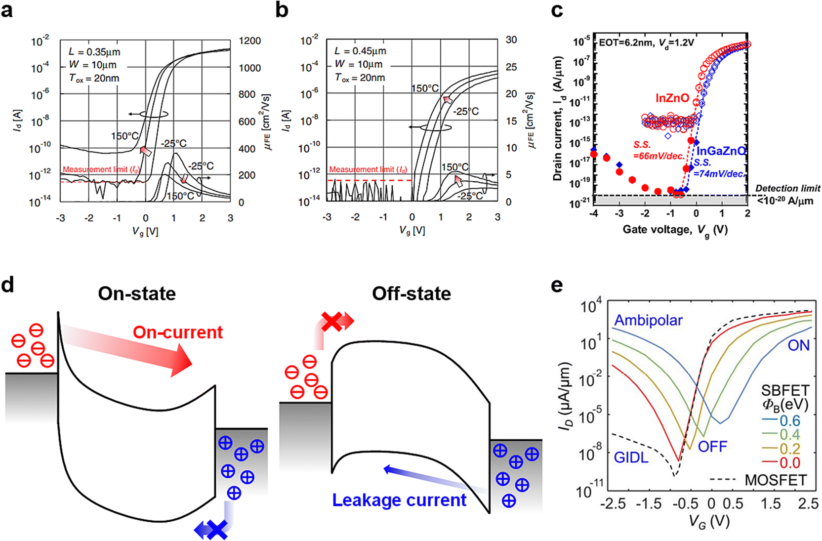 | ||
| Fig. 3 Temperature dependent transfer characteristics of (a) Si and (b) CAAC-IGZO FETs.64 The off-currents of the OS FETs were below the measurement limit regardless of the temperature. (c) Transfer characteristics of OS TFTs with ultralow off-current (measured by circuit voltage drop).60 (d) Band diagram illustrations of on and off states in TMD FETs. Leakage current occurs in the off state. (e) Transfer characteristics of TMD FETs with different SBH. Ambipolarity-induced leakage current is significantly higher than GIDL.65 | ||
In comparison to silicon and OSs, TMDs demonstrate higher off-current characteristics, primarily due to the inherent ambipolar behavior exhibited by TMDs. In the context of n-channel TMD FETs, the application of a negative gate voltage elevates the SBH for electrons, reducing their injection and aiding in turn-off. However, this configuration leads to a decrease in the Schottky barrier width for holes, increasing the tunnelling probability of holes and resulting in high off-current (refer to Fig. 3d). Ambipolar behavior-induced leakage is also observed in p-channel TMD FETs. In contrast, silicon-based FETs, which operate with PN junctions and are unipolar, and OS FETs, characterized by a larger bandgap and lower hole concentration, do not exhibit ambipolarity. As a result, they show lower off-current compared to TMD FETs.8 The investigation of leakage currents, such as GIDL, subthreshold leakage, and junction leakage, has been limited in TMD FETs due to the challenges posed by ambipolarity (as shown in Fig. 3e). Nevertheless, GIDL and junction leakage in TMD FETs are expected to be relatively low considering the larger bandgap of TMDs compared to silicon. Conversely, subthreshold leakage is anticipated to be high due to the elevated Dit.65,66 Consequently, research efforts aimed at mitigating ambipolarity should be given priority.
3. Issues to overcome
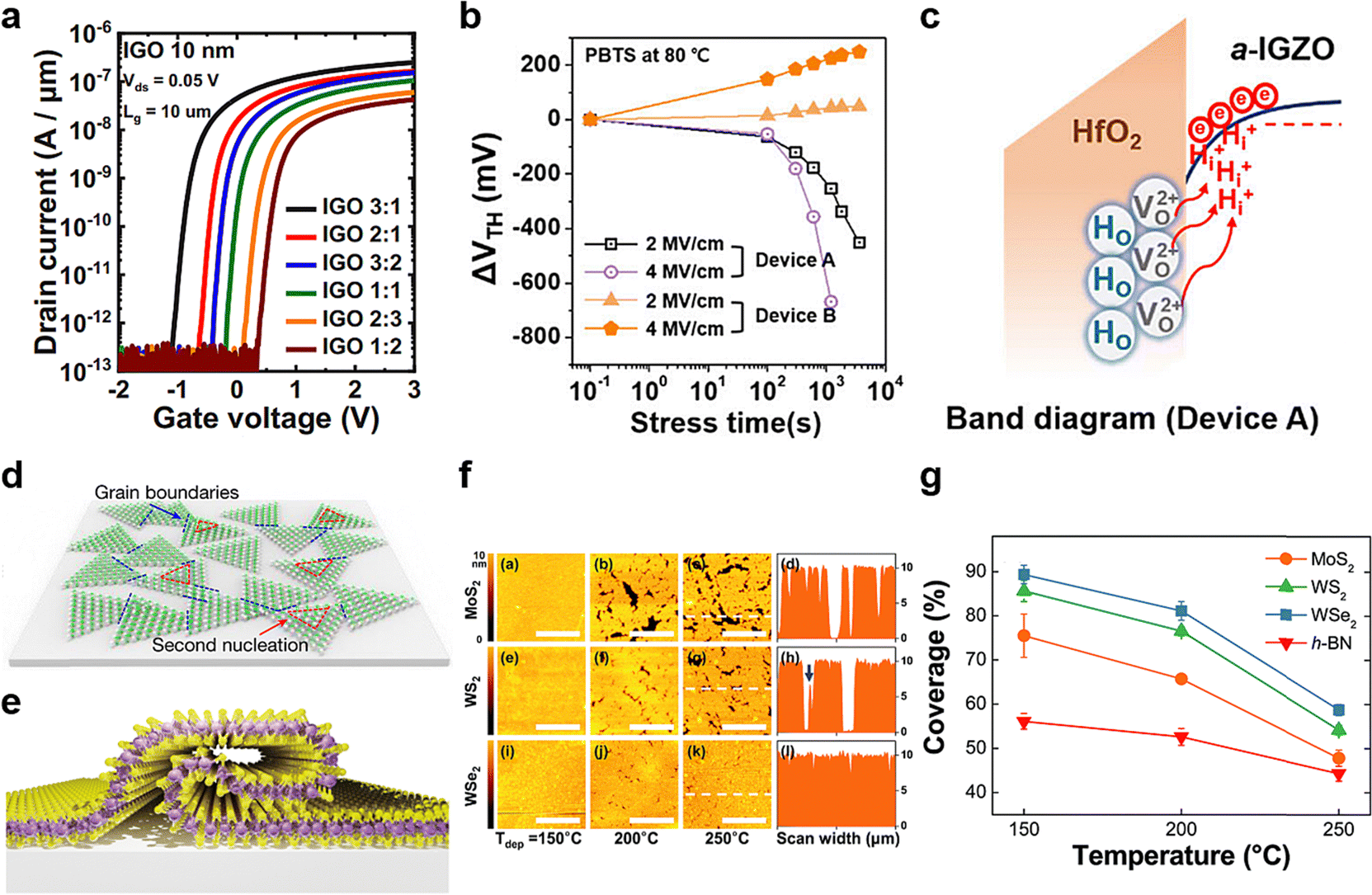 | ||
| Fig. 4 (a) Comparison of IGO FETs depending on the In–Ga composition ratio.27 (b) PBTS comparison of device A (single HfO2 layer as gate insulator) and device B (SiO2/HfO2 multilayer as a gate insulator including O2 annealing). (c) Possible mechanism of stability degradation for device A (singe HfO2 layer as gate insulator).41 (d) Grain boundaries and (e) wrinkles formed during TMD growth.68,69 (f) Atomic force microscopy (AFM) topography images and height profiles of Al2O3 grown on MoS2 and (g) surface coverage.70 | ||
D. Application to DRAM
As elucidated in the previous section, a discernible trend is emerging in the assessment of OS-based DRAM characteristics, driven by the excellent step-coverage capabilities of ALD processes and the ultra-low off-current exhibited by OSs. A recent contribution by Belmonte et al. exemplifies this trajectory, where the implementation of a 2T0C DRAM cell achieved an extraordinary diminutive off-current of <3 × 10⁻²¹ A μm−1 and a long retention time of >4.5 hours through meticulous process optimization of OS FETs.72 Furthermore, Chen et al. made noteworthy strides by introducing a 2T0C cell transistor based on a vertically stacked CAA FET structure, featuring a 4F2 feature size and endurance characteristics exceeding >1012 cycles due to the exceptionally low off-currents of the OS FETs.73 These findings underscore the potential of OS FET technology in next-generation DRAM, showing superior power efficiency and performance compared to traditional Si-based technologies. This paradigm shift is poised to exert a profound influence on the trajectory of future research and development endeavors in the 3D DRAM.E. Perspectives
While certain challenges remain, the potential applications of OS and TMD channels extend beyond DRAM. The application of OSs extends beyond volatile memory to include frequent proposals for next-generation memories such as FeFET.74,75 This is attributed to the OS's low off-current and the potential improvement in interface characteristics compared to silicon-based ferroelectrics. However, even in the application of components beyond DRAM, contact-limited behavior of OSs mentioned in part C and the need for improvement in hydrogen immunity continue to act as bottlenecks that require further enhancement. Despite the development of various memory devices using TMDs, their specific application in DRAM remains limited.76–78 Also discussed in Part C, significant efforts are required to utilize TMDs as channel materials in DRAM cell transistors. These efforts should primarily concentrate on reducing interface and bulk trap density while mitigating ambipolarity-induced leakage current to minimize off-current and enhance SS.F. Conclusion
We discussed the structures proposed for 3D DRAM architectures to date, the applicability of TMDs and OSs to 3D DRAM, and research on 3D DRAM with such materials, especially OSs. Samsung and Hynix proposed structures in which a horizontal capacitor is connected to a GAA FET and a double gate FET, respectively. Micron, on the other hand, presented a structure where a vertical capacitor is connected to a CAA FET. Ongoing research efforts aim to incorporate OSs and TMDs, next-generation semiconductor materials, into these 3D cell transistors. We explored the feasibility of applying OSs and TMDs in 3D DRAM through a comparative analysis of their properties. OSs are celebrated for their ultra-low off-current and low SS characteristics, as evidenced by recent achievements of OS-based DRAM. Nevertheless, there remains ample room for additional research, particularly in areas such as enhancing mobility, reducing electrical contact resistivity, and improving H-related thermal bias instabilities. TMDs exhibit outstanding conductivity characteristics, leading to a high on-current. However, ambipolarity-induced leakage current occurs in the off-state, resulting in elevated off-current characteristics. Therefore, further research is essential to address the leakage current associated with ambipolarity.Conflicts of interest
The authors declare no conflicts of interests.Acknowledgements
This research was supported by the National Research Foundation of Korea (NRF) (2022M3F3A2A01072215, 2021R1A2C2010026, and RS-2023-00235609). This work was also supported by the Institute of Information & communications Technology Planning & Evaluation (IITP) under the Artificial Intelligence Semiconductor Support Program to Nurture the Best Talents (IITP-2024-RS-2023-00253914) grant funded by the Korean government.References
- S. Sivaram, Presented in part at IEEE Symposium on VLSI Technology and Circuits (VLSI Technology and Circuits), Kyoto, Japan, June, 2023.
- A. Spessot and H. Oh, IEEE Trans. Electron Devices, 2020, 67(4), 1382–1393 CAS
.
- S.-K. Park, Presented in part at IEEE International Memory Workshop (IMW), Monterey, CA, USA, May, 2015.
- M. J. Kim, H. J. Park, S. Yoo, M. H. Cho and J. K. Jeong, IEEE Trans. Electron Devices, 2022, 69(5), 2409–2416 CAS
- U. Chand, Presented in part at IEEE Symposium on VLSI Technology and Circuits (VLSI Technology and Circuits), Honolulu, HI, USA, June, 2022.
- C. J. Dorow, Presented in part at IEEE International Electron Devices Meeting (IEDM), San Francisco, CA, USA, Dec., 2022.
- W. Lu, Presented in part at IEEE International Electron Devices Meeting (IEDM), San Francisco, CA, USA, Dec., 2022.
- T. Kim, C. H. Choi, J. S. Hur, D. Ha, B. J. Kuh, Y. Kim, M. H. Cho, S. Kim and J. K. Jeong, Adv. Mater., 2023, 35(43), 2204663 CrossRef CAS PubMed
- S.-K. Su, C.-P. Chuu, M.-Y. Li, C.-C. Cheng, H. S. P. Wong and L.-J. Li, Small Structures, 2021, 2(5), 2000103 CrossRef CAS
- J. Y. Kim, Presented in part at IEEE Symposium on VLSI Technology, Kyoto, Japan, June, 2003.
- T. Schloesser, Presented in part at IEEE International Electron Devices Meeting (IEDM), San Francisco, CA, USA, Dec., 2008.
- H. Chung, Presented in part at IEEE European Solid-State Device Research Conference (ESSDERC), Helsinki, Finland, Sept., 2011.
- T. Tran, Presented in part at IEEE International Electron Devices Meeting (IEDM), San Francisco, CA, USA, Dec., 2023.
-
J. Kim, K. Lee, B.-S. Kim, J. Kim, D. Woo, K. Lee, H. S. Hong and Y. Hwang, US Pat., 10,535,659, 2020 Search PubMed
-
H. Yoon and S. H. Kim, US Pat., 17/957,147, 2022 Search PubMed
-
D. V. N. Ramaswamy, US Pat., 11,011,529, 2021 Search PubMed
- J. W. Han, Presented in part at IEEE Symposium on VLSI Technology and Circuits (VLSI Technology and Circuits), Kyoto, Japan, June, 2023.
- D. Ha, Presented in part at IEEE Symposium on VLSI Technology and Circuits (VLSI Technology and Circuits), Honolulu, HI, USA, June, 2022.
- A. Belmonte, Presented in part at IEEE International Electron Devices Meeting (IEDM), San Francisco, CA, USA, Dec., 2020.
- D. Geng, K. Wang, L. Li, K. Myny, A. Nathan, J. Jang, Y. Kuo and M. Liu, Nat. Electron., 2023, 6, 963–972 CrossRef CAS
- H. Hosono, J. Non-Cryst. Solids, 2006, 352(9–20), 851–858 CrossRef CAS
- T. Hong, Y.-S. Kim, S.-H. Choi, J. H. Lim and J.-S. Park, Adv. Electron. Mater., 2023, 9(4), 2201208 CrossRef CAS
- A. Charnas, Z. Zhang, Z. Lin, D. Zheng, J. Zhang, M. Si and P. D. Ye, Adv. Mater., 2024, 36(9), 2304044 CrossRef CAS PubMed
- Ü. Özgür, Y. I. Alivov, C. Liu, A. Teke, M. A. Reshchikov, S. Doğan, V. Avrutin, S.-J. Cho and H. Morkoç, J. Appl. Phys., 2005, 98(4), 041301 CrossRef
- J. S. Hur, M. J. Kim, S. H. Yoon, H. Choi, C. K. Park, S. H. Lee, M. H. Cho, B. J. Kuh and J. K. Jeong, ACS Appl. Mater. Interfaces, 2022, 14(43), 48857–48867 CrossRef CAS PubMed
- D. Zheng, Presented in part at IEEE International Electron Devices Meeting (IEDM), San Francisco, CA, USA, Dec., 2022.
- K. Hikake, Presented in part at IEEE Symposium on VLSI Technology and Circuits (VLSI Technology and Circuits), Kyoto, Japan, June, 2023.
- G.-B. Kim, N. On, T. Kim, C. H. Choi, J. S. Hur, J. H. Lim and J. K. Jeong, Small Methods, 2023, 7(7), 2201522 CrossRef CAS PubMed
- B. J. Park, S. W. Chung, M. J. Kim, H. J. Lee, J. H. Bae, S. C. Kang and J. K. Jeong, IEEE Electron Device Lett., 2023, 44(11), 1857–1860 CAS
- K. S. Novoselov, A. K. Geim, S. V. Morozov, D. Jiang, Y. Zhang, S. V. Dubonos, I. V. Grigorieva and A. A. Firsov, Science, 2004, 306(5696), 666–669 CrossRef CAS PubMed
- A. K. Geim and I. V. Grigorieva, Nature, 2013, 499, 419–425 CrossRef CAS PubMed
- S. Manzeli, D. Ovchinnikov, D. Pasquier, O. V. Yazyev and A. Kis, Nat. Rev. Mater., 2017, 2, 17033 CrossRef CAS
- L. Liu, Y. Lu and J. Guo, IEEE Trans. Electron Devices, 2013, 60(12), 4133–4139 CAS
- H. J. Seul, M. J. Kim, H. J. Yang, M. H. Cho, M. H. Cho, W.-B. Song and J. K. Jeong, ACS Appl. Mater. Interfaces, 2020, 12(30), 33887–33898 CrossRef CAS PubMed
- M. H. Cho, C. H. Choi, H. J. Seul, H. C. Cho and J. K. Jeong, ACS Appl. Mater. Interfaces, 2021, 13(14), 16628–16640 CrossRef CAS PubMed
- H. J. Yang, H. J. Seul, M. J. Kim, Y. Kim, H. C. Cho, M. H. Cho, Y. H. Song, H. Yang and J. K. Jeong, ACS Appl. Mater. Interfaces, 2020, 12(47), 52937–52951 CrossRef CAS PubMed
- M. Si, Z. Lin, Z. Chen, X. Sun, H. Wang and P. D. Ye, Nat. Electron., 2022, 5, 164–170 CrossRef CAS
- M. Si, Y. Hu, Z. Lin, X. Sun, A. Charnas, D. Zheng, X. Lyu, H. Wang, K. Cho and P. D. Ye, Nano Lett., 2021, 21(1), 500–506 CrossRef CAS PubMed
- Z. Zhang, Presented in part at IEEE International Electron Devices Meeting (IEDM), San Francisco, CA, USA, Dec., 2022.
- C.-Y. Jeong, H.-J. Kim, J. I. Kim, J.-H. Lee and H.-I. Kwon, J. Vac. Sci. Technol., B, 2016, 34, 060601 CrossRef
- C. H. Choi, T. Kim, M. J. Kim, S. H. Yoon and J. K. Jeong, IEEE Trans. Electron Devices, 2023, 70(5), 2317–2323 CAS
- J. Li, Y. Guan, J. Li, Y. Zhang, Y. Zhang, M. Chan, X. Wang, L. Lu and S. Zhang, Nanotechnology, 2023, 34(26), 265202 CrossRef PubMed
- Z. Wu, J. Niu, C. Lu, Z. Bai, K. Chen, Z. Wu, W. Lu, M. Liu, F. Liao, D. Geng, N. Lu, G. Yang and L. Li, IEEE Electron Device Lett., 2024, 45(3), 408–411 Search PubMed
- Q. Li, Presented in part at IEEE International Electron Devices Meeting (IEDM), San Francisco, CA, USA, Dec., 2022.
- H. Tang, H. Dekkers, N. Rassoul, S. Sutar, S. Subhechha, V. Afanas’ev, J. V. Houdt, R. Delhougne, G. S. Kar and A. Belmonte, IEEE Trans. Electron Devices, 2024, 71(1), 567–573 CAS
- J. Kataoka, N. Saito, T. Ueda, T. Tezuka, T. Sawabe and K. Ikeda, Jpn. J. Appl. Phys., 2019, 58, SBBJ03 CrossRef CAS
- C.-S. Pang, T. Y. T. Hung, A. Khosravi, R. Addou, Q. Wang, M. J. Kim, R. M. Wallace and Z. Chen, Adv. Electron. Mater., 2020, 6(8), 1901304 CrossRef CAS
- P.-C. Shen, C. Su, Y. Lin, A.-S. Chou, C.-C. Cheng, J.-H. Park, M.-H. Chiu, A.-Y. Lu, H.-L. Tang, M. M. Tavakoli, G. Pitner, X. Ji, Z. Cai, N. Mao, J. Wang, V. Tung, J. Li, J. Bokor, A. Zettl, C.-I. Wu, T. Palacios, L.-J. Li and J. Kong, Nature, 2021, 593, 211–217 CrossRef CAS PubMed
- Y. Zhu, Y. Li, G. Arefe, R. A. Burke, C. Tan, Y. Hao, X. Liu, X. Liu, W. J. Yoo, M. Dubey, Q. Lin and J. C. Hone, Nano Lett., 2018, 18(6), 3807–3813 CrossRef CAS PubMed
- Z. Ahmed, Presented in part at IEEE International Electron Devices Meeting (IEDM), San Francisco, CA, USA, Dec., 2020.
- J. Park, H. Jung, W. Kwon, G. Choi, J. Chang and J. Jeon, ACS Appl. Electron. Mater., 2023, 5(4), 2239–2248 CrossRef CAS
- D. S. Schulman, A. J. Arnold and S. Das, Chem. Soc. Rev., 2018, 47, 3037–3058 RSC
- Y. Zheng, J. Gao, C. Han and W. Chen, Cell Rep., 2021, 2(1), 100298 CAS
- G. Kwon, Y.-H. Choi, H. Lee, H.-S. Kim, J. Jeong, K. Jeong, M. Baik, H. Kwon, J. Ahn, E. Lee and M.-H. Cho, Nat. Electron., 2022, 5, 241–247 CrossRef CAS
- A. Allain, J. Kang, K. Banerjee and A. Kis, Nat. Mater., 2015, 14, 1195–1205 CrossRef CAS PubMed
- W. Li, X. Gong, Z. Yu, L. Ma, W. Sun, S. Gao, C. Koroglu, W. Wang, L. Liu, T. Li, H. Ning, D. Fan, Y. Xu, X. Tu, T. Xu, L. Sun, W. Wang, J. Lu, Z. Ni, J. Li, X. Duan, P. Wang, Y. Nie, H. Qiu, Y. Shi, E. Pop, J. Wang and X. Wang, Nature, 2023, 613, 274–279 CrossRef CAS PubMed
- Z. Yu, Z.-Y. Ong, Y. Pan, Y. Cui, R. Xin, Y. Shi, B. Wang, Y. Wu, T. Chen, Y.-W. Zhang, G. Zhang and X. Wang, Adv. Mater., 2016, 28(3), 547–552 CrossRef CAS PubMed
- M. Takenaka, Presented in part at IEEE International Electron Devices Meeting (IEDM), San Francisco, CA, USA, Dec., 2016.
- Y. Y. Illarionov, T. Knobloch, M. Jech, M. Lanza, D. Akinwande, M. I. Vexler, T. Mueller, M. C. Lemme, G. Fiori, F. Schwierz and T. Grasser, Nat. Commun., 2020, 11, 3385 CrossRef CAS PubMed
- N. Saito, T. Sawabe, J. Kataoka, T. Ueda, T. Tezuka and K. Ikeda, Jpn. J. Appl. Phys., 2019, 58, SBBJ07 CrossRef CAS
- H. Kunitake, K. Ohshima, K. Tsuda, N. Matsumoto, T. Koshida, S. Ohshita, H. Sawai, Y. Yanagisawa, S. Saga, R. Arasawa, T. Seski, R. Honda, H. Baba, D. Shimada, H. Kimura, R. Tokumaru, T. Atsumi, K. Kato and S. Yamazaki, IEEE J. Electron Devices Soc., 2019, 7, 495–502 CAS
- Q. Hu, C. Gu, S. Zhu, Q. Li, A. Tong, J. Kang, R. Huang and Y. Wu, IEEE Electron Device Lett., 2023, 44(1), 60–63 CAS
- K. Kato, Y. Shionoiri, Y. Sekine, K. Furutani, T. Hatano, T. Aoki, M. Sasaki, H. Tomatsu, J. Koyama and S. Yamazaki, Jpn. J. Appl. Phys., 2012, 51, 021201 CrossRef
- S. Yamazaki, H. Suzawa, K. Inoue, K. Kato, T. Hirohashi, K. Okazaki and N. Kimizuka, Jpn. J. Appl. Phys., 2014, 53, 04ED18 CrossRef
- J. Kang, Presented in part at IEEE International Electron Devices Meeting (IEDM), San Francisco, CA, USA, Dec., 2017.
- J. Chang, presented in part at International Conference on Simulation of Semiconductor Processes and Devices (SISPAD), Glasgow, UK, Sept., 2013.
- Q. Wang, R. Shi, Y. Zhao, R. Huang, Z. Wang, A. Amini and C. Cheng, Nanoscale Adv., 2021, 3, 3430–3440 RSC
- S. H. Choi, S. J. Yun, Y. S. Won, C. S. Oh, S. M. Kim, K. K. Kim and Y. H. Lee, Nat. Commun., 2022, 13, 1484 CrossRef CAS PubMed
- K. S. Kim, D. Lee, C. S. Chang, S. Seo, Y. Hu, S. Cha, H. Kim, J. Shin, J.-H. Lee, S. Lee, J. S. Kim, K. H. Kim, J. M. Suh, Y. Meng, B.-I. Park, J.-H. Lee, H.-S. Park, H. S. Kum, M.-H. Jo, G. Y. Yeom, K. Cho, J.-H. Park, S.-H. Bae and J. Kim, Nature, 2023, 614, 88–94 CrossRef CAS PubMed
- T. Park, H. Kim, M. Leem, W. Ahn, S. Choi, J. Kim, J. Uh, K. Kwon, S.-J. Jeong, S. Park, Y. Kim and H. Kim, RSC Adv., 2017, 7, 884–889 RSC
- K. M. Price, K. E. Schauble, F. A. McGuire, D. B. Farmer and A. D. Franklin, ACS Appl. Mater. Interfaces, 2017, 9(27), 23072–23080 CrossRef CAS PubMed
- A. Belmonte, Presented in part at IEEE Symposium on VLSI Technology and Circuits (VLSI Technology and Circuits), Kyoto, Japan, June, 2023.
- C. Chen, Presented in part at IEEE International Electron Devices Meeting (IEDM), San Francisco, CA, USA, Dec., 2022.
- M. Zeng, Presented in part at IEEE International Electron Devices Meeting (IEDM), San Francisco, CA, USA, Dec., 2023.
- C.-K. Chen, presented in part at IEEE International Electron Devices Meeting (IEDM), San Francisco, CA, USA, Dec., 2022.
- K. A. Nirmal, W. Ren, A. C. Khot, D. Y. Kang, T. D. Dongale and T. G. Kim, Adv. Sci., 2023, 10(19), 2300433 CrossRef CAS PubMed
- N. B. Mullani, D. D. Kumbhar, D.-H. Lee, M. J. Kwon, S. Cho, N. Oh, E.-T. Kim, T. D. Dongale, S. Y. Nam and J. H. Park, Adv. Funct. Mater., 2023, 33(26), 2300343 CrossRef CAS
- L. Yin, R. Cheng, Y. Wen, C. Liu and J. He, Adv. Mater., 2021, 33(29), 2007081 CrossRef CAS PubMed
Footnote |
| † These authors contributed equally to the paper. |
| This journal is © The Royal Society of Chemistry 2024 |