
Selective activation of MoS2 grain boundaries for enhanced electrochemical activity†
Radha
Raman
 abcd,
Jeyavelan
Muthu
bde,
Zhi-Long
Yen
bcf,
Mohammad
Qorbani
gh,
Yu-Xiang
Chen
bcf,
Ding-Rui
Chen
bcf,
Mario
Hofmann
*d and
Ya-Ping
Hsieh
*b
abcd,
Jeyavelan
Muthu
bde,
Zhi-Long
Yen
bcf,
Mohammad
Qorbani
gh,
Yu-Xiang
Chen
bcf,
Ding-Rui
Chen
bcf,
Mario
Hofmann
*d and
Ya-Ping
Hsieh
*b
aDepartment of Physics, National Central University, Taoyuan 32001, Taiwan
bInstitute of Atomic and Molecular Sciences, Academia Sinica, Taipei 10617, Taiwan. E-mail: yphsieh@gate.sinica.edu.tw
cMolecular Science and Technology Program, Taiwan International Graduate Program, Academia Sinica, Taipei 10617, Taiwan
dDepartment of Physics, National Taiwan University, Taipei 10617, Taiwan
eNanoscience and Technology Program, Taiwan International Graduate Program, Academia Sinica, Taipei 115, Taiwan. E-mail: mario@phys.ntu.edu.tw
fInternational Graduate Program of Molecular Science and Technology, National Taiwan University, Taipei, 10617, Taiwan
gCenter for Condensed Matter Sciences, National Taiwan University, Taipei 10617, Taiwan
hCenter of Atomic Initiative for New Materials, National Taiwan University, Taipei 10617, Taiwan
First published on 4th March 2024
Abstract
Molybdenum disulfide (MoS2) has emerged as a promising material for catalysis and sustainable energy conversion. However, the inertness of its basal plane to electrochemical reactions poses challenges to the utilization of wafer-scale MoS2 in electrocatalysis. To overcome this limitation, we present a technique that enhances the catalytic activity of continuous MoS2 by preferentially activating its buried grain boundaries (GBs). Through mild UV irradiation, a significant enhancement in GB activity was observed that approaches the values for MoS2 edges, as confirmed by a site-selective photo-deposition technique and micro-electrochemical hydrogen evolution reaction (HER) measurements. Combined spectroscopic characterization and ab-initio simulation demonstrates substitutional oxygen functionalization at the grain boundaries to be the origin of this selective catalytic enhancement by an order of magnitude. Our approach not only improves the density of active sites in MoS2 catalytic processes but yields a new photocatalytic conversion process. By exploiting the difference in electronic structure between activated GBs and the basal plane, homo-compositional junctions were realized that improve the photocatalytic synthesis of hydrogen by 47% and achieve performances beyond the capabilities of other catalytic sites.
New conceptsThe exceptional characteristics of two-dimensional (2D) materials, particularly MoS2, make them highly suitable for photocatalysis. The primary challenge in harnessing the full potential of MoS2 lies in its low intrinsic catalytic activity. Traditional methods have attempted to alter the morphology of MoS2 by introducing defects or edges. Unfortunately, these approaches reduce the exciton separation efficiency and limit the photocatalytic efficiency. Our study introduces a novel approach that relies on activating the existing defects in MoS2, particularly the grain boundaries. Conventional grain boundaries show a turnover frequency 75 times lower than that of edge sites. We have developed a technique that significantly enhances their activity to levels comparable with MoS2 edges, as confirmed through detailed site-resolved photoreduction experiments and selective microelectrochemical measurements. Additionally, our research includes site-selective characterization using local electrochemical measurements of overpotential and Tafel slope, which yielded results analogous to photoreduction analysis, thus demonstrating the utility of this simpler method. This approach not only enhances the catalytic performance of MoS2 but also provides an exciting route toward tailoring 2D materials for future photocatalysts, with our findings showing a substantial increase in photocatalytic efficiency. |
Introduction
2D semiconductors have emerged as highly promising materials for photocatalytic applications.1–3 The reduced dimensionality and quantum confinement effects increase their light–matter interaction and enhance the lifetime of photogenerated electron–hole pairs, thus providing an efficient route for photocarrier generation. MoS2 has gained significant attention due to the suitability of its active sites for catalytic hydrogen evolution,4,5 positioning it as a highly promising material for sustainable, solar-powered energy conversion.Unfortunately, the active sites in MoS2 are mainly localized at the edges and its basal plane is two orders less efficient.6–8 To enhance the overall efficiency of MoS2, researchers have increased the edge concentration by enhancing the porosity of MoS29,10 but at the cost of increased process complexity and decreased efficiency of photo-excited carrier transport.11 To take advantage of the large relative concentration of basal plane sites compared to edges, significant ongoing research efforts are dedicated toward developing innovative strategies to activate the MoS2 basal plane. These strategies include surface modifications, defect engineering through functionalization,12 and hybridization with other materials.13–16 While the introduction of defects is a practical route towards higher catalytic activity, the increased defect density introduces non-radiative recombination pathways and affects the exciton separation leading to a decreased photocatalytic efficiency.17
We here enhance the electrochemical performance of MoS2 through activation of its grain boundaries. Grain boundaries are an important feature of 2D materials that occur due to parallel nucleation during chemical vapor deposition (CVD) growth or polycrystallinity of the bulk precursors for exfoliation.18 These extended one-dimensional structures are embedded within the basal plane but possess distinct electronic properties.19–22 Activation of grain boundaries in MoS2 could offer abundant active sites while not impeding charge separation thereby improving photocatalytic activity.
To date, however, grain boundaries have not received significant attention as photocatalytically active structures. High-resolution electrochemical microscopy by Lunardon et al. observed a limited activity of grain boundaries.23 Moreover, Takahashi et al. found that the activity was inhomogeneous along the grain boundaries.24 Finally, He et al. demonstrated that intrinsic grain boundaries are inferior in HER performance compared to morphology-controlled nanograin edges.25
In this study, a novel route for enhancing the catalytic performance of grain boundaries is presented. By utilizing a UV-assisted activation process, these features showed a selective enhancement in electrocatalytic properties, as revealed by photoreduction experiments and location-resolved electrochemical measurements. Spectroscopic characterization reveals changes to the composition as the origin of this behavior and its limitation to grain boundaries. This novel mechanism was exploited to produce lateral homojunction in MoS2 that enhances its photocatalytic HER performance beyond the activity of MoS2 edges, which had been considered the optimal morphology. Our study reveals the role of grain boundaries in catalytic processes and provides a promising route toward the development of efficient 2D materials-based photocatalytic systems.
Results and discussions
Light-driven photoreduction provides a powerful route to establish the spatial variation in 2D materials’ electrochemical activity.26,27 Illumination causes electrons to be photoexcited and acquire enough energy to reduce ions in a solution. This hypothesis is confirmed by the observation that no decoration from an aqueous HAuCl4 solution (1 mM) occurs on MoS2 under dark conditions (Fig. 1(a)). However, upon illumination, we observe a significant deposition of gold particles by atomic force microscopy at specific locations while other regions remain undecorated (Fig. 1(c)). The location of the photoreduction is determined by the heterogeneous reaction rate between 2D material and electrolyte and we find significant deposition at the edges of the MoS2 flake (Fig. 1(b)). This selective decoration agrees with previous reports that transition metal dichalcogenide (TMD) edges exhibit two-order higher reactivity than the basal plane.8,28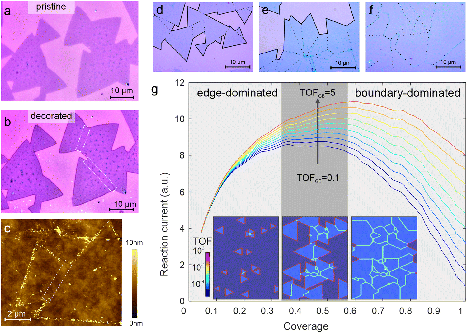 | ||
| Fig. 1 Visualization of catalytic active sites in pristine MoS2: (a) micrographs of MoS2 flakes exposed to HAuCl4 containing electrolyte under dark conditions, (b) micrograph of same area as (a) after illumination demonstrating predominant deposition on edges and limited deposition on grain boundaries (indicated by dashed boxes) and basal plane, (c) atomic force micrograph after illumination demonstrating the selective deposition of nanoparticles at the MoS2 flake edge, (d)–(f) optical micrographs of MoS2 at different coverage with indication of edges (solid lines) and grain boundaries (dotted lines) indicating increased grain boundary concentration, (g) simulation of total electrochemical HER activity at variable MoS2 coverage showing transition from edge-dominated to boundary-dominated activity, different traces correspond to different values of grain boundary activity (inset) representative spatial activity map at different grain morphologies. | ||
Upon closer inspection, it can be seen that many flakes do not consist of a single triangular crystal but are composed of several triangular regions (Fig. 1(a and b)). As identified previously, such arrangements represent joint polycrystalline structures that not only exhibit edges but also grain boundaries.29 Careful characterization of the deposition density suggests a ∼75-fold lower decoration density on grain boundaries compared to that of edges (see ESI† for more details). This quantification agrees with previous reports that found two orders of magnitude lower activity of grain boundaries compared to edges.8,25
Our results demonstrate the limitations of the electrochemical activity of 2D MoS2 films: as the grain density increases, the number of active edge sites increases and so does the electrochemical activity. However, upon reaching a critical density, merging of individual crystalline flakes occurs and their edges turn into grain boundaries, which exhibit a significantly lower turn-over-frequency. This behavior is captured in numerical simulations shown in Fig. 1(g). Grain growth from randomly distributed nucleation seeds was simulated and the total turn-over-frequency of the area was calculated. As expected, an initial increase in activity was observed when the edge concentration is increased. However, a transition to boundary-controlled activity can be seen at higher coverage that decreases the overall activity despite an increase in MoS2 coverage (see ESI† for more details).
Our simulations not only demonstrate the current limitations in 2D materials-based electrocatalysis but also provide a route to overcoming them: if the grain boundary activity could be increased, a significant enhancement in overall activity could be achieved.
To enhance the grain boundary activity, we utilized fast adsorption of UV-generated oxygen. For this purpose, the MoS2 sample was exposed to UV-generated ozone for 2 minutes (see method section for more details). Following this treatment, the experiment involving Au deposition was carried out in a dark environment, and no observable deposits were noted within a 60-second timeframe (Fig. 2(a)). Subsequently, the photoreduction experiments were conducted and we observed a significant increase in gold decoration (Fig. 2(b)). Compared to the un-activated condition, activation not only enhances the amount of deposition at the grain boundaries but also decorates all grain boundaries within the structure. This result demonstrates the potential of grain boundary activation to overcome the previously observed issue of inhomogeneous grain boundary activity.24
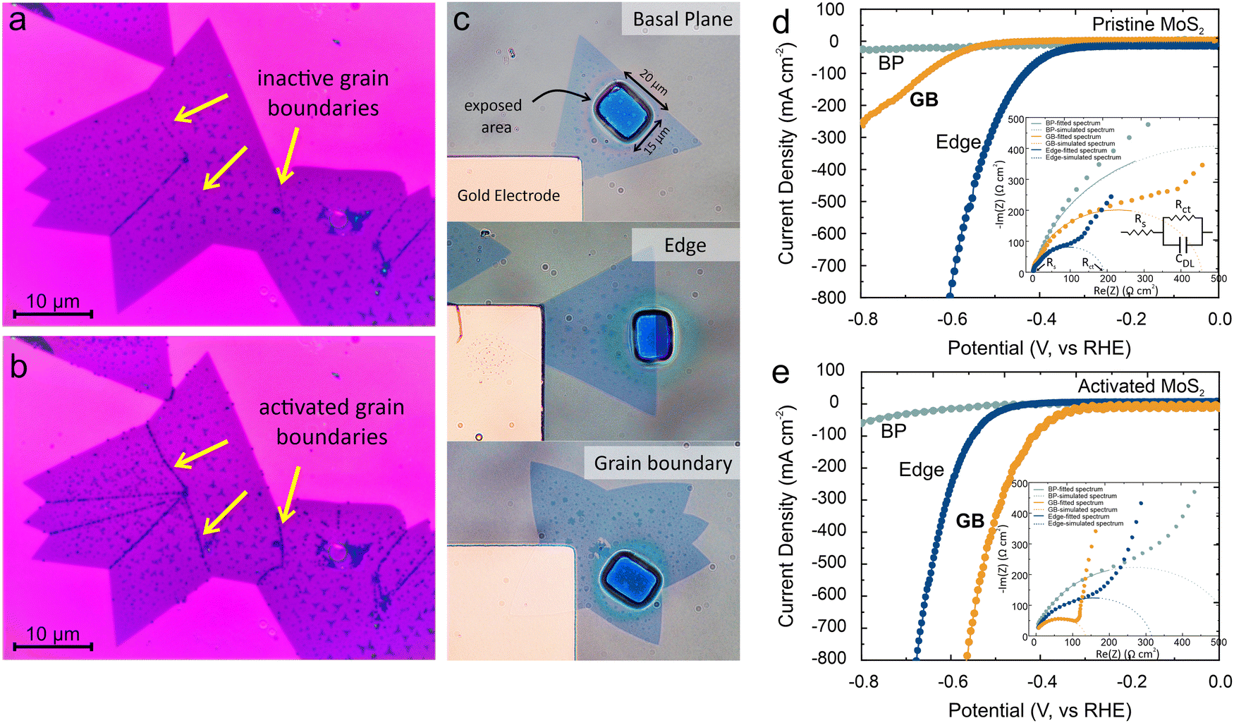 | ||
| Fig. 2 Impact of grain boundary activation on catalytic performance: (a) micrograph of photodecoration on MoS2 flake before activation, (the contrast in (a) is attributed to adlayers formed during the CVD process) (b) photodecoration after grain boundary activation showing enhanced deposition, (c) micrograph of the electrochemical microelectrode setup with selective exposure of MoS2 features (i.e. basal plane, edge and grain-boundary, respectively) (d) polarization curves of all three features without activation, (inset) EIS Nyquist plots of all 3 features, (e) polarization curve for all 3 features after activation, (inset) EIS Nyquist plots. All current and impedance values are normalized to the exposed electrode area. | ||
To quantify the observed enhancement of the grain boundary's catalytic activity, we conducted spatially selective electrochemical characterization of hydrogen evolution reaction (HER). For this purpose, we lithographically produced openings with dimensions of 20 μm × 15 μm, allowing us to target and analyze the catalytic activity of different regions on MoS2 (Fig. 2(c)). (more details on the electrochemical reactor and fabrication are in the methods section)
Linear sweep voltammetry measurements were conducted on samples that selectively exposed MoS2 edges, grain boundaries, or the basal plane as shown in Fig. 2(d). We observed distinct differences in the HER activities of those regions. The pristine MoS2 basal plane exhibited poor HER activity, attributed to its perfect crystal structure that results in a limited number of active sites, consistent with previous experimental findings.30 In contrast, the MoS2 edges displayed enhanced HER activities as evidenced by a ∼3-fold lowered overpotential and a ∼7-fold decreased Tafel slope (Fig. 2(d)) (see ESI† section S3 for corresponding Tafel plots). These results confirm the superior catalytic activity of the edges in as-grown MoS2. Notably, the as-grown MoS2 grain boundaries exhibit an overpotential that is comparable to the basal plane and a Tafel slope that is intermediate between the basal plane and edges. This observed trend is consistent with the photodeposition results, where enhanced deposition of Au was observed at the edges, followed by the grain boundaries, while minimal deposition occurred on the basal plane. A quantitative agreement between deposition density of Au clusters and electrochemical activity of each catalytic site was observed that follows previous report8 (see ESI† section S1 for more details)
Upon UV activation, MoS2 electrochemical activity shows significant changes (Fig. 2(e)): We find that the polarization curve for the basal-plane remains unchanged, which indicates that the short exposure and low reactivity of UV ozone are insufficient to generate active sites in the inert crystal. Surprisingly, the MoS2 edge shows an increased overpotential and Tafel slope which can be understood by the reported detrimental effect of oxygen adsorption on HER performance of MoS2 edges.31 This poisoning effect limits the performance of electrocatalysts under realistic conditions.32
Grain boundaries, on the other hand, do not exhibit such a deactivation and we extract a two-fold decrease in overpotential and a two-fold decrease in Tafel slope compared to the pristine values. These parameters rival the performance of pristine edges and validate our envisioned MoS2 catalytic enhancement. The observed enhancement of the reaction current indicates that thus-activated MoS2 can yield reaction efficiencies that are comparable to commercial Pt catalysts.6,33
The observed enhancement is confirmed by electrochemical impedance spectroscopy (EIS) measurements (inset Fig. 2(d) and (e)). The heterogeneous charge transfer resistance of boundaries is found to be decreased by 67% and reaches similar values to that of pristine edges.
To examine the activation mechanism that leads to the observed enhanced catalytic performance of grain boundaries we conduct Raman spectroscopy. Raman spectrum shows characteristic peaks corresponding to the A1g mode at ∼404 cm−1 and the E12g mode at ∼384 cm−1 as expected for MoS2 (Fig. 3(a)). The difference in these peak positions is Δω of ∼20 cm−1 and depends on the introduction of in-plane strain, brought about by changes in thickness,34,35 compositional changes,36,37 or charge transfer-induced stiffening of the bonds.38,39
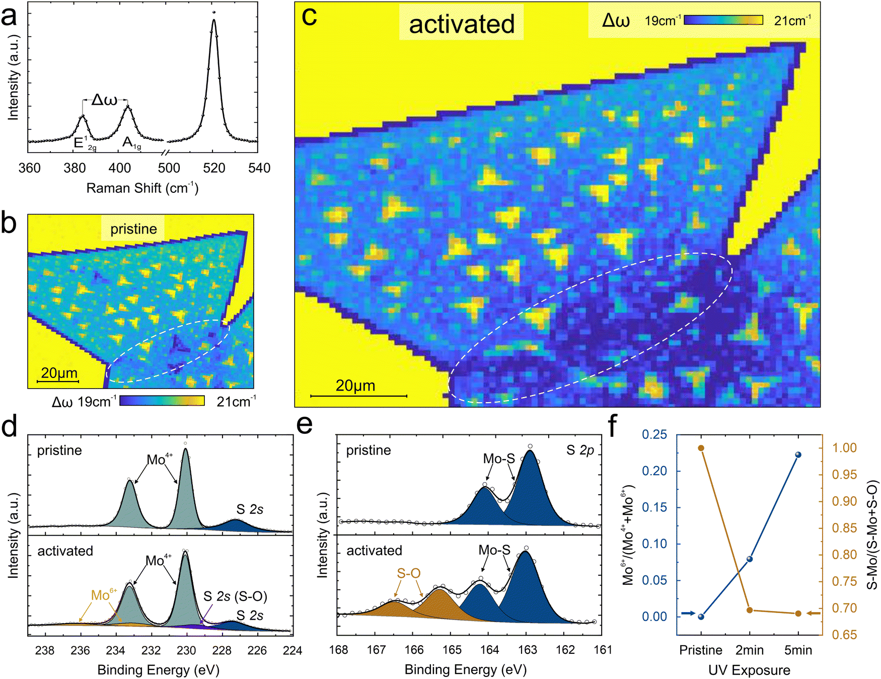 | ||
| Fig. 3 Spectroscopic characterization of UV-oxidized MoS2: (a) representative Raman spectrum of MoS2 illustrating the peak separation Δω between E12g and A1g modes of ∼20 cm−1. (b) and (c) Time evolution of the spatial distribution of Δω for pristine MoS2 and activated MoS2, showing a significant shift at GB region (c), (d) XPS spectra of Mo 3d revealing increased MoO3 content upon activation (e) S 2p region exhibiting changes over UV exposure time. (f) the relative amount of MoO3 and Mo-bonded S as a function of activation time. | ||
The spatially resolved Raman map demonstrates differences in Δω between the edge and basal plane that indicate the presence of dangling bonds.40 (Fig. 3(b)). Moreover, the occurrence of multilayers can be distinguished from the Raman maps. However, no difference between the basal plane and the expected grain boundary location is observed.
After a 2-minute UV treatment, a significant decrease in Δω at the grain boundary can be observed (Fig. 3(c)) and the value is comparable to the edge region. This behavior suggests that UV exposure modifies the grain boundaries and introduces compositional changes or doping. Finally, longer oxygen adsorption durations upshift the Δω of both grain boundary and edges. (see ESI† section S4 for more details)
X-ray photoelectron spectroscopy (XPS) was conducted to provide details about the modification that grain boundaries undergo during activation. High-resolution spectra of the Mo 3d region were acquired that exhibit characteristic peaks at binding energies of 230.08 and 233.23 eV, corresponding to the Mo4+ 3d5/2 and Mo4+ 3d3/2 spin–orbit split components, respectively. (Fig. 3(d)) Upon 2 minutes of UV treatment, the spectra reveal the emergence of distinctive doublets at higher binding energies, indicative of the presence of Mo6+ species associated with MoO3 formation. After 5 minutes of adsorption, the intensity of the Mo6+ doublet further increases, suggesting a significant conversion of the surface to MoO3. Concurrently, the S 2p region displays peak broadening, indicating a change in chemical order and the formation of MoS2−xOx (Fig. 3(e)). This behavior confirms the selective reaction of grain boundaries with UV at mild activation conditions.29,41 The reaction of UV-generated ozone initially produces covalently bonded sulfur and oxygen structures at the boundary and subsequent loss of S resulting in an oxygen-saturated vacancy18,42,43
To understand the impact of the observed oxidative GB functionalization on the catalytic performance of MoS2, we conduct simulations using density functional theory (DFT). The Gibbs free energy of hydrogen adsorption (ΔGH) was investigated due to its significance in establishing the HER efficiency.44 We calculated the ΔGH for three systems – the MoS2 basal plane, a MoS2 edge and three stable grain boundary types (Mo-4|8, S-8|8 and S-4|8) (Fig. 4(a)) (ESI† info for more details about calculation).45
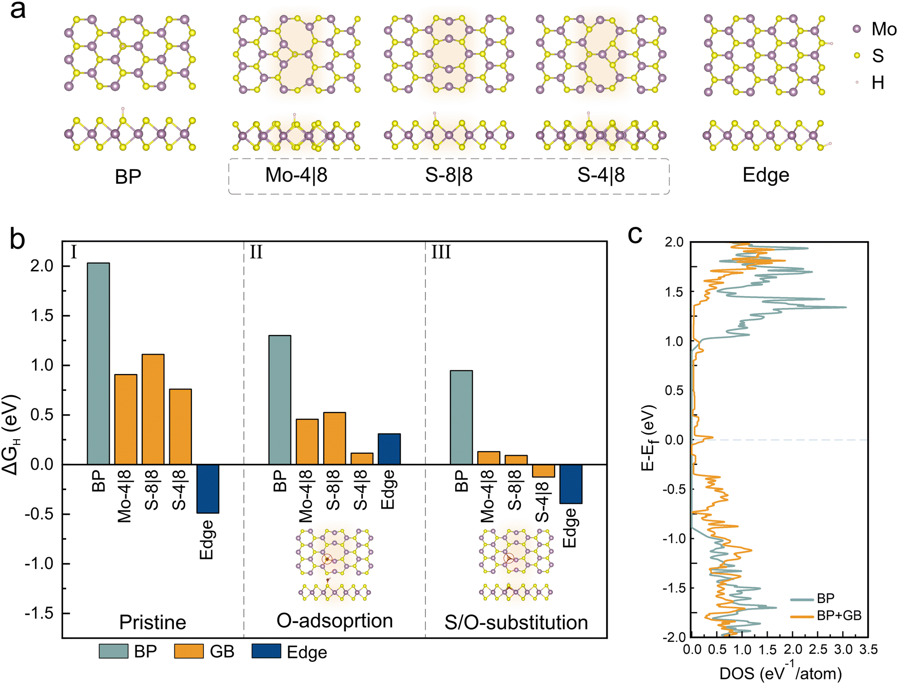 | ||
| Fig. 4 Gibbs free energy calculations for hydrogen adsorption: (a) depiction of hydrogen adsorption in configurations representing the basal plane, 3 different types of grain boundaries and MoS2 edge, (b) calculated Gibbs free energy ΔGH for hydrogen adsorption at various sites, examined under different conditions: pristine (section I), oxygen-adsorbed (section II) and oxygen-substituted (section III) (more details in the ESI†); the inset shows the oxygen adsorption and substitution site for the S-8|8 system (c) comparison of the density of states between pristine MoS2 and the system with an introduced grain boundary. | ||
The results of these simulations are shown in Fig. 4(b) and we observe a value of 2.03 eV for ΔGH of the basal plane which indicates a weak bonding of hydrogen that limits the adsorption efficiency and consequently lowers the HER.46 Conversely, the MoS2 edge exhibits a superior catalytic performance due to ΔGH being closer to zero. Regardless of type, all MoS2 grain boundaries are found to exhibit a lower HER efficiency than the MoS2 edge which agrees with our experimental findings.
Subsequently, oxygen was introduced in a chemisorbed configuration. For this purpose, oxygen was positioned close to a sulfur site and relaxed (details in the ESI,† Fig. S6, ESI†). We observe that this step increases the activity of all systems which is ascribed to charge transfer that enhances the adsorption of protons from the acidic electrolyte.47
Finally, to reproduce the electron spectroscopic results of activated GBs, oxygen was introduced substitutionally in sulfur vacancies on all three systems. We observe that this modification indeed lowers the ΔGH for GBs by up to 12 times compared to the pristine case. This effect is much larger for grain boundaries than for edges or the basal plane and can explain the observed selective activation of grain boundaries. This selectivity can be understood when comparing the density of states for MoS2 BP and GB system (Fig. 4(c)). A higher density of states close to the Fermi level indicates the potential of GBs for enhanced electrochemical interactions.48
One promising application of MoS2 is in the direct conversion of sunlight to green hydrogen.49 To identify the potential of our grain-boundary activation scheme for this purpose, we conduct photoluminescence (PL) spectroscopy. Upon oxygen adsorption, grain boundaries exhibit a decreased photoluminescence yield (Fig. 5(a)). This decrease in yield is found to be due to the enhanced concentration of trions at the grain boundary compared to the basal plane and indicates the accumulation of charge carriers (inset Fig. 5(a)).
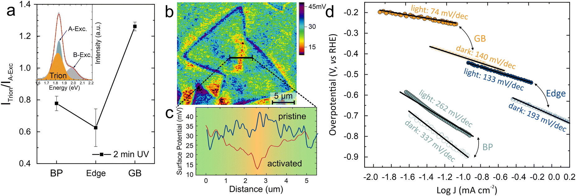 | ||
| Fig. 5 Photo-electrocatalytic performance of GB activated MoS2: (a) trion/exciton ratio at different sites of MoS2 flakes indicating GBs having high accumulation of charges, (inset) representative PL spectra of MoS2 with decomposition into exciton and trion peaks (b) KPFM surface potential map of activated MoS2 flake indicating a substantial potential dip at GB (c) corresponding cross-sectional plot for pristine and activated GB region (more details in ESI†), (d) photo-electrochemical performance of UV activated MoS2 indicating the improved contribution of GBs under light condition. | ||
This accumulation was characterized by Kelvin probe force microscopy (KPFM) which provides a map of the contact potential difference (CPD) (Fig. 5(b)). We observe that the pristine grain boundary does not exhibit a significant difference in CPD compared to the basal plane. After 2 minutes of oxygen adsorption, however, the surface potential map revealed a noteworthy potential dip at the grain boundaries, signifying a change in the electronic structure at these regions. Under light illumination, the photons are absorbed by the MoS2 and excited electron–hole pairs are separated under the build-in electric field at the grain boundary. (Fig. 5(c))
The observed selective control over the grain boundary potential represents a promising approach for producing lateral homojunction in the MoS2. Previous work has demonstrated the attractiveness of such structures for enhancing a 2D material's photocatalytic properties as it enhances exciton separation and carrier lifetime.50,51
To confirm the prospect of grain-boundary-based homojunction, we characterize the photo-electrocatalytic performance of different MoS2 features. For this purpose, the Tafel slope was extracted for grain-boundary activated MoS2 regions under dark conditions and white light illumination (more details are provided in the methods section). While the basal plane and edges exhibit a slight change in Tafel slope under illumination, the creation of a homojunction around the grain boundary leads to a notable 47% reduction in the Tafel slope (Fig. 5(d)). This performance is superior even to the photocatalytic efficiency of MoS2 edges and demonstrates the potential of our activation approach.
Conclusion
In conclusion, our study highlights the potential of grain-boundary activation to enhance the photocatalytic properties of MoS2. Through site-selective photodeposition and electrochemical measurements, the limited intrinsic activity of grain boundaries was established. A short exposure to mild oxidizing conditions resulted in the selective formation of oxygen-substituted sulfur vacancies at grain boundaries which increases their activity by several times as confirmed by ab-initio calculations. The resulting spatially varying charge distribution enables a novel lateral heterojunction that enhances the photocatalytic performance of MoS2 grain boundaries beyond the abilities of other active sites. Our results increase the understanding of catalysis in 2D materials and present a facile route for the design of high-performance photocatalysts.Experimental section
CVD Growth of MoS2
MoS2 flakes were synthesized using mediator mediator-assisted recipe as described previously.52 Briefly, the MoO3 precursor (50 nm) was pre-deposited on graphite using an e-beam evaporator.To initiate the growth process, a solution of NaCl + NaOH was spin-coated onto the SiO2/Si substrate and dried for 5 minutes at 90 °C. The SiO2/Si substrate was then placed facedown onto a holey graphite spacer on the MoO3/graphite structure to form a sandwich structure.
The growth process was conducted in a three-stage heating process, where the temperature was increased from room temperature to 700 °C in 20 minutes, and then from 700 °C to 900 °C in 10 minutes. The growth temperature was maintained at 900 °C for 10 minutes, and diluted hydrogen sulfide (99% diluted in Ar) continuously flowed into the reactor at atmospheric pressure during the growth period.
The growth temperature was then reduced to 830 °C in 20 minutes, and the H2S flow was turned off. The furnace was allowed to cool naturally to room temperature.
Optical microscopy observations
The bright field and the dark field image were collected via an optical microscope (Olympus, BX53), with a CCD camera attached to it.Au photodeposition
A 1.0 mM solution of HAuCl4 was prepared by dissolving the compound in DI water. The area of interest on a MoS2 substrate was focused using a microscope, and a 2 μL solution of Au containing 20% Methanol as a hole scavenger was deposited on it via a micropipette. The white light source of an optical microscope was utilized as an illumination source for the photodeposition of Au on MoS2 at an irradiation intensity of approximately 5 mW cm−2. The intensity of the illumination source was adjusted using magnifying lenses. Following the photodeposition experiment, the excess electrolyte was gently removed by blotting the surface with a clean tissue, leaving no residue. Finally, the sample was imaged using a camera for subsequent analysis.UV ozone treatment
To achieve controlled oxidation of MoS2, we employed a custom-built UV-O3 cleaner equipped with two UV lamps (185 & 254 nm), each operating at a specified power of 20 W.PL and Raman measurements
Raman and photoluminescence (PL) measurements were performed using a custom-built microscopic Raman and PL system equipped with a 532 nm laser (1.5 mW). Raman and PL mapping was conducted on a flake containing grain boundaries (GBs), and subsequently, data from the pixels corresponding to the edge, basal plane, and GBs were extracted using Matlab and analyzed.XPS measurement
X-ray photoelectron spectroscopy (XPS) measurements were conducted at room temperature using a PHI5000 Versa Probe apparatus equipped with an Al Kα X-ray source. The XPS peak was calibrated with C 1s (284.6 eV). Gaussian–Lorentzian line shapes was used for the fitting of the spectra. The binding energies of the recorded spectra were calibrated using the C 1s peak at 284.6 eV. CasaXPS software (version 2.3.20), with the Gaussian–Lorentzian GL(m) line shapes and an error of ± 0.05 eV, was used to fit the XPS signals of the S 2p (with the spin–orbit splitting of Δ = 1.20 eV), S 2s, and Mo 3d (with the spin–orbit splitting of Δ = 3.15 eV) orbitals with the relative sensitivity factors (RSFs) of 0.717, 0.426, and 3.54, respectively. So, given the peak area of the S 2p spectrum, we calculated the peak area of the S 2s orbital in the Mo 3d windows. Additionally, we adjusted the line shapes, i.e., m in the GL(m) function, by utilizing the “Test Peak Model” in the CasaXPS software. The x value in MoSx was calculated using the S–Mo and Mo4+ peak areas in S 2p and Mo 3d, respectively.KPFM measurement
KPFM measurements were conducted using a Bruker Dimension Icon atomic force microscope, operating under standard ambient conditions. KPFM enabled us to quantitatively map the distribution of contact potential difference (CPD) with nanometer-scale resolution, providing valuable insights into the local surface potential variations. For the measurements, a silicon cantilever tip coated with platinum–iridium (SCM-PIT, Bruker Co.) was employed in tapping mode.The KPFM setup used a dual-pass approach, where the first pass recorded the topography profile using tapping mode. In the second line scan, an alternating current (AC) voltage of 500 mV amplitude was applied to the AFM tip while maintaining an optimized lift height of 25![[thin space (1/6-em)]](https://www.rsc.org/images/entities/char_2009.gif) nm above the topographical baseline, facilitating the mapping of the surface potential.
nm above the topographical baseline, facilitating the mapping of the surface potential.
The measured CPD represents the contact potential difference between the sample and the tip and is expressed by the following equation:
| CPD = (ϕsample – ϕtip)/q |
Device fabrication for HER measurements
The photocatalytic activity of various MoS2 flakes was measured using a fabricated device. The fabrication process involved multiple lithography steps and masking to expose the area of interest. Firstly, the substrate with MoS2 flakes was spin-coated with photoresist at 1000 rpm for 10 s and 4000 rpm for 30 s, followed by baking at 90 °C for 90 s. Electrode patterns were then defined on different regions of the flakes, including the Edge, Basal plane, and GBs. Thermal evaporator is then used to deposit Cr/Au at a rate of 0.5 Å s−1. After the lift-off process, metallic electrodes were obtained to provide electrical connections between different parts of the flakes.To create a micro-reactor, another lithography step was performed, exposing windows of 15 μm × 20 μm on the target regions (Edge, Basal plane, and GBs), followed by development and cleaning. Finally, the devices were baked at 200 °C for 10 min to ensure no leakage under the protection layer.
HER Measurement
To test the micro-electrocatalysis and photocatalysis performance of MoS2 flakes, a three-electrode system was used in conjunction with a CHI660E electrochemical workstation. A platinum wire with a diameter of 0.2 mm was used as a counter electrode, while an Ag wire with a diameter of 0.2 mm coated with AgCl served as a quasi-reference electrode. The working electrode was an exposed area of 15 μm × 20 μm on each type of region, including Edge, Basal plane, and GBs. The hydrogen evolution reaction (HER) activity of each device was evaluated in 0.5 M H2SO4 electrolyte using linear sweep voltammetry at a scan rate of 5 mV s−1. A xenon lamp (Schott ACE I, A20500, 150 watts) was used as a light source for the photocatalytic measurements.All potential values were converted to reversible hydrogen electrode potentials using the relation E (vs. RHE) = E (vs. Ag/AgCl) + 0.197 V + V (quasi) + 0.0591, and the data were corrected by taking into account the potential drop on the materials and electrolyte. This comprehensive testing protocol allowed for a thorough evaluation of the photocatalytic performance of MoS2 flakes in different regions and under varying conditions, providing valuable insights for the development and optimization of advanced photocatalytic systems.
Electrochemical impedance spectroscopy (EIS) measurement
Electrochemical impedance spectra (EIS) were collected using the same experimental setup at a perturbation voltage amplitude of 50 mV, within the frequency range of 1 kHz to 1 MHz. To estimate the solution resistance (Rs) and charge transfer resistance (Rct), the Nyquist curve was fitted using an equivalent circuit.Computational details
First-principles calculations based on density functional theory (DFT) were conducted utilizing the QuantumATK software.53 Generalized gradient approximation (GGA) with the Perdew–Burke–Ernzerhof (PBE) functional was selected to account for exchange–correlation interactions. To accurately represent core electrons, we employed norm-conserving pseudopotentials obtained from the PseudoDojo library.The vacuum along c-axis was set to 20 Å above the MoS2 plane to avoid any periodic interaction. The in-plane separation between the longitudinal edges across the periodic boundary is set to be greater than the 20 Å to the avoid the any artificial effect arising from the edge–edge interaction.
For the geometry optimization and total energy calculation, we adopted the linear combination of atomic orbitals (LCAO) formalism with localized orbitals. A density-mesh cutoff of 75 Hartree was utilized to ensure precise results. Geometry optimizations were carried out using the QuantumATK-optimized Medium basis set.
We employed a Monkhorst–Pack (MP) grid with dimensions of 1 × 3 × 1 Γ-centered for all our simulations. Additionally, for computing the density of states (DOS), a 1 × 5 × 1 MP grid was selected.
To ensure convergence during structural relaxation, we set a criterion for the residual force on each atom at 0.02eV Å−1. Geometries were systematically relaxed to minimize the total energy of the system until a precision of 10−4 eV was achieved.
Author contributions
Radha Raman: conceptualization, methodology, validation, formal analysis, investigation, data curation, writing – original draft. Jeyavelan Muthu: methodology, validation. Zhi-Long Yen: investigation. Mohammad Qorbani: formal analysis. Yu-Xiang Chen: resources. Ding-Rui Chen: resources. Mario Hofmann: conceptualization, software, formal analysis, writing – review & editing. Ya-Ping Hsieh: writing – review & editing, supervision, project administration, funding acquisition.Associated content
More details on methods, extended characterization, and simulation are provided in the ESI.†Funding Sources
M. H. acknowledges funding through the National Science and Technology Council NSTC (110-2628-M-002 -005 and 110-2124-M-002 -018). Y. H. acknowledges funding through Academia Sinica (AS-GCS-112-M04) and National Science and Technology Council NSTC 112-2112-M-001-051.Conflicts of interest
There are no conflicts to declare.Acknowledgements
The authors extend their heartfelt gratitude to Jing-Jong Shyue (Research Fellow, Research Center for Applied Sciences Academia Sinica) for their generous provision of access to their advanced X-ray Photoelectron Spectroscopy (XPS) instrument. The authors would like to thank Taiwan Semiconductor Research Institute (TSRI), Taiwan for providing access to the QauntumATK.References
- A. B. Laursen, S. Kegnæs, S. Dahl and I. Chorkendorff, Energy Environ. Sci., 2012, 5, 5577–5591 RSC.
- D. Voiry, M. Salehi, R. Silva, T. Fujita, M. Chen, T. Asefa, V. B. Shenoy, G. Eda and M. Chhowalla, Nano Lett., 2013, 13, 6222–6227 CrossRef CAS PubMed.
- C. Wu, J. Zhang, X. Tong, P. Yu, J. Xu, J. Wu, Z. M. Wang, J. Lou and Y. Chueh, Small, 2019, 15, 1900578 CrossRef PubMed.
- Z. Liang, R. Shen, Y. H. Ng, P. Zhang, Q. Xiang and X. Li, J. Mater. Sci. Technol., 2020, 56, 89–121 CrossRef CAS.
- D. Merki and X. Hu, Energy Environ. Sci., 2011, 4, 3878–3888 RSC.
- T. F. Jaramillo, K. P. Jørgensen, J. Bonde, J. H. Nielsen, S. Horch and I. Chorkendorff, Science, 2007, 317, 100–102 CrossRef CAS PubMed.
- L. Jiang, Q. Zhou, J.-J. Li, Y.-X. Xia, H.-X. Li and Y.-J. Li, ACS Appl. Nano Mater., 2022, 5, 3521–3530 CrossRef CAS.
- G. Li, D. Zhang, Q. Qiao, Y. Yu, D. Peterson, A. Zafar, R. Kumar, S. Curtarolo, F. Hunte and S. Shannon, J. Am. Chem. Soc., 2016, 138, 16632–16638 CrossRef CAS PubMed.
- D. Ko, X. Jin, K.-d Seong, B. Yan, H. Chai, J. M. Kim, M. Hwang, J. Choi, W. Zhang and Y. Piao, Appl. Catal., B, 2019, 248, 357–365 CrossRef CAS.
- Z. Wu, B. Fang, Z. Wang, C. Wang, Z. Liu, F. Liu, W. Wang, A. Alfantazi, D. Wang and D. P. Wilkinson, ACS Catal., 2013, 3, 2101–2107 CrossRef CAS.
- D.-R. Chen, J. Muthu, X.-Y. Guo, H.-T. Chin, Y.-C. Lin, G. Haider, C.-C. Ting, M. Kalbáč, M. Hofmann and Y.-P. Hsieh, J. Mater. Chem. A, 2023, 11, 15802–15810 RSC.
- N. Wang, L. Cheng, Y. Liao and Q. Xiang, Small, 2023, 2300109 CrossRef CAS PubMed.
- Q. Liang, Q. Zhang, X. Zhao, M. Liu and A. T. Wee, ACS Nano, 2021, 15, 2165–2181 CrossRef CAS PubMed.
- G. Ye, Y. Gong, J. Lin, B. Li, Y. He, S. T. Pantelides, W. Zhou, R. Vajtai and P. M. Ajayan, Nano Lett., 2016, 16, 1097–1103 CrossRef CAS PubMed.
- X. Zhang, F. Zhou, S. Zhang, Y. Liang and R. Wang, Adv. Sci., 2019, 6, 1900090 CrossRef PubMed.
- H. Zhang, L. Yu, T. Chen, W. Zhou and X. W. Lou, Adv. Funct. Mater., 2018, 28, 1807086 CrossRef.
- L. Li and E. A. Carter, J. Am. Chem. Soc., 2019, 141, 10451–10461 CrossRef CAS PubMed.
- A. M. Van Der Zande, P. Y. Huang, D. A. Chenet, T. C. Berkelbach, Y. You, G.-H. Lee, T. F. Heinz, D. R. Reichman, D. A. Muller and J. C. Hone, Nat. Mater., 2013, 12, 554–561 CrossRef CAS PubMed.
- S. Chen, J. Gao, B. M. Srinivasan, G. Zhang, M. Yang, J. Chai, S. Wang, D. Chi and Y.-W. Zhang, ACS Appl. Mater. Interfaces, 2019, 11, 46090–46100 CrossRef CAS PubMed.
- J. Cheng, T. Jiang, Q. Ji, Y. Zhang, Z. Li, Y. Shan, Y. Zhang, X. Gong, W. Liu and S. Wu, Adv. Mater., 2015, 27, 4069–4074 CrossRef CAS PubMed.
- L. Karvonen, A. Säynätjoki, M. J. Huttunen, A. Autere, B. Amirsolaimani, S. Li, R. A. Norwood, N. Peyghambarian, H. Lipsanen and G. Eda, Nat. Commun., 2017, 8, 15714 CrossRef CAS PubMed.
- S. Park, M. S. Kim, H. Kim, J. Lee, G. H. Han, J. Jung and J. Kim, ACS Nano, 2015, 9, 11042–11048 CrossRef CAS PubMed.
- M. Lunardon, T. Kosmala, M. Ghorbani-Asl, A. V. Krasheninnikov, S. Kolekar, C. Durante, M. Batzill, S. Agnoli and G. Granozzi, ACS Energy Lett., 2023, 8, 972–980 CrossRef CAS PubMed.
- Y. Takahashi, Y. Kobayashi, Z. Wang, Y. Ito, M. Ota, H. Ida, A. Kumatani, K. Miyazawa, T. Fujita and H. Shiku, Angew. Chem., Int. Ed., 2020, 59, 3601–3608 CrossRef CAS PubMed.
- Y. He, P. Tang, Z. Hu, Q. He, C. Zhu, L. Wang, Q. Zeng, P. Golani, G. Gao and W. Fu, Nat. Commun., 2020, 11, 57 CrossRef CAS PubMed.
- T. Daeneke, B. Carey, A. Chrimes, J. Z. Ou, D. Lau, B. Gibson, M. Bhaskaran and K. Kalantar-Zadeh, J. Mater. Chem. C, 2015, 3, 4771–4778 RSC.
- I. Song, Y. Kim, B. H. Lee, M. Chae, S. Kim, C. Yoon, M.-K. Joo, J. Shin, S. M. Kim and C. Ko, Nanomaterials, 2022, 12, 3549 CrossRef CAS PubMed.
- M. Qorbani, A. Sabbah, Y.-R. Lai, S. Kholimatussadiah, S. Quadir, C.-Y. Huang, I. Shown, Y.-F. Huang, M. Hayashi and K.-H. Chen, Nat. Commun., 2022, 13, 1256 CrossRef CAS PubMed.
- Y. Rong, K. He, M. Pacios, A. W. Robertson, H. Bhaskaran and J. H. Warner, ACS Nano, 2015, 9, 3695–3703 CrossRef CAS PubMed.
- Y. Cao, ACS Nano, 2021, 15, 11014–11039 CrossRef CAS PubMed.
- L. Sharma, T. Botari, C. S. Tiwary and A. Halder, ACS Appl. Energy Mater., 2020, 3, 5333–5342 CrossRef CAS.
- C. S. Lim, S. M. Tan, Z. Sofer and M. Pumera, ACS Nano, 2015, 9, 8474–8483 CrossRef CAS PubMed.
- J. N. Hansen, H. Prats, K. K. Toudahl, N. Mørch Secher, K. Chan, J. Kibsgaard and I. Chorkendorff, ACS Energy Lett., 2021, 6, 1175–1180 CrossRef CAS PubMed.
- T.-X. Huang, X. Cong, S.-S. Wu, K.-Q. Lin, X. Yao, Y.-H. He, J.-B. Wu, Y.-F. Bao, S.-C. Huang and X. Wang, Nat. Commun., 2019, 10, 5544 CrossRef CAS PubMed.
- M. Velicky, A. Rodriguez, M. Bousa, A. V. Krayev, M. Vondracek, J. Honolka, M. Ahmadi, G. E. Donnelly, F. Huang and H. D. Abruna, J. Phys. Chem. Lett., 2020, 11, 6112–6118 CrossRef CAS PubMed.
- S. Gupta, A. Johnston and S. Khondaker, J. Appl. Phys., 2022, 131, 164303 CrossRef CAS.
- T. Y. Ko, A. Jeong, W. Kim, J. Lee, Y. Kim, J. E. Lee, G. H. Ryu, K. Park, D. Kim and Z. Lee, 2D Mater., 2016, 4, 014003 CrossRef.
- P.-C. Shen, Y. Lin, C. Su, C. McGahan, A.-Y. Lu, X. Ji, X. Wang, H. Wang, N. Mao and Y. Guo, Nat. Electron., 2022, 5, 28–36 CrossRef CAS.
- R. Rao, A. E. Islam, S. Singh, R. Berry, R. K. Kawakami, B. Maruyama and J. Katoch, Phys. Rev. B, 2019, 99, 195401 CrossRef CAS.
- W. L. Chow, X. Luo, S. Q. Quek and B. K. Tay, Adv. Electron. Mater., 2015, 1, 1400037 CrossRef.
- C. Jung, H. I. Yang and W. Choi, Nanoscale Res. Lett., 2019, 14, 1–8 CrossRef CAS PubMed.
- A. N. Enyashin, M. Bar-Sadan, L. Houben and G. Seifert, J. Phys. Chem. C, 2013, 117, 10842–10848 CrossRef CAS.
- M. H. Rahman, E. H. Chowdhury and S. Hong, Surf. Interfaces, 2021, 26, 101371 CrossRef CAS.
- B. Seo, G. Y. Jung, Y. J. Sa, H. Y. Jeong, J. Y. Cheon, J. H. Lee, H. Y. Kim, J. C. Kim, H. S. Shin and S. K. Kwak, ACS Nano, 2015, 9, 3728–3739 CrossRef CAS PubMed.
- S. Wang, B. Huang, Y. Dai and W. Wei, J. Phys. Chem. C, 2022, 126, 6215–6222 CrossRef CAS.
- K. S. Exner, Electrochem. Sci. Adv., 2022, 2, e2100101 CrossRef CAS.
- J. Pető, T. Ollár, P. Vancsó, Z. I. Popov, G. Z. Magda, G. Dobrik, C. Hwang, P. B. Sorokin and L. Tapasztó, Nat. Chem., 2018, 10, 1246–1251 CrossRef PubMed.
- Y. Ouyang, C. Ling, Q. Chen, Z. Wang, L. Shi and J. Wang, Chem. Mater., 2016, 28, 4390–4396 CrossRef CAS.
- J. Shi, D. Ma, G.-F. Han, Y. Zhang, Q. Ji, T. Gao, J. Sun, X. Song, C. Li and Y. Zhang, ACS Nano, 2014, 8, 10196–10204 CrossRef CAS PubMed.
- A. Castellanos-Gomez, R. Roldán, E. Cappelluti, M. Buscema, F. Guinea, H. S. Van Der Zant and G. A. Steele, Nano Lett., 2013, 13, 5361–5366 CrossRef CAS PubMed.
- F.-H. Hsiao, C.-C. Chung, C.-H. Chiang, W.-N. Feng, W.-Y. Tzeng, H.-M. Lin, C.-M. Tu, H.-L. Wu, Y.-H. Wang and W.-Y. Woon, ACS Nano, 2022, 16, 4298–4307 CrossRef CAS PubMed.
- Y.-S. Chen, S.-K. Chiu, D.-L. Tsai, C.-Y. Liu, H.-A. Ting, Y.-C. Yao, H. Son, G. Haider, M. Kalbáč and C.-C. Ting, npj 2D Mater. Appl., 2022, 6, 54 CrossRef CAS.
- S. Smidstrup, T. Markussen, P. Vancraeyveld, J. Wellendorff, J. Schneider, T. Gunst, B. Verstichel, D. Stradi, P. A. Khomyakov and U. G. Vej-Hansen, J. Phys.: Condens. Matter, 2019, 32, 015901 CrossRef PubMed.
Footnote |
| † Electronic supplementary information (ESI) available. See DOI: https://doi.org/10.1039/d4nh00005f |
| This journal is © The Royal Society of Chemistry 2024 |