
Physical reservoirs based on MoS2–HZO integrated ferroelectric field-effect transistors for reservoir computing systems†
Lingqi
Li‡
,
Heng
Xiang‡
,
Haofei
Zheng
,
Yu-Chieh
Chien
,
Ngoc Thanh
Duong
,
Jing
Gao
and
Kah-Wee
Ang
 *
*
Department of Electrical and Computer Engineering, National University of Singapore, 4 Engineering Drive 3, Singapore 117583. E-mail: eleakw@nus.edu.sg
First published on 11th March 2024
Abstract
Reservoir computing (RC), a variant of recurrent neural networks (RNNs), is well-known for its reduced energy consumption through exclusive focus on training the output weight and its superior performance in handling spatiotemporal information. Implementing these networks in hardware requires devices with superior fading memory behavior. Unlike filament-based two-terminal devices, those relying on ferroelectric switching demonstrate improved voltage reliability, while three-terminal transistors provide additional active control. HfO2-based ferroelectric materials such as Hf0.5Zr0.5O2 (HZO), have garnered attention for their scalability and seamless integration with CMOS technology. This study implements a RC hardware based on MoS2–HZO integrated device structure with enhanced spontaneous polarization field. By adjusting the oxygen vacancy concentration, the devices exhibit consistent responses to both identical and nonidentical voltages, making them suitable for diverse RC applications. The high accuracy of MNIST handwritten digits recognition highlights the rich reservoir states of the traditional RC architecture. Additionally, the impact of masks on RC implementation is assessed, showcasing the device's capability for spatiotemporal signal analysis. This development paves the way for implementing energy-efficient and high-performance computing solutions.
New conceptsThis manuscript systematically presents, for the first time, the optimization of device structure and thin-film deposition to realize an MoS2–HZO integrated FeFET designed for diverse real-life tasks within an RC system. Recognized for its energy-saving capabilities, RC stands out as one of the most efficient neuromorphic computing algorithms. However, given the inherent passive control in reservoirs based on two-terminal devices, actively managing a stable physical reservoir becomes imperative for the implementation of RC systems based on physical devices. The selection of HZO as the ferroelectric material proves advantageous due to its scalability and compatibility with CMOS processes. While HZO exhibits spontaneous depolarization, its impact on retention becomes significant only when the strength of this depolarization electric field surpasses the coercive field (EC). Through careful optimization of the device structure, the intrinsic depolarization electric field within HZO is enhanced, resulting in a volatile behavior. Additionally, the generation of reservoir states hinges on the nonlinear reversal of ferroelectric domains in the polycrystalline structure of HZO, which corresponds to the voltage intensity and pulse duration. Tuning the deposition process of HZO can influence its phase formation, subsequently affecting the flipping behavior of the ferroelectric domains. Therefore, selecting appropriate deposition conditions is crucial for the adaptability of the device to different systems. This proof-of-concept demonstration opens new possibilities for the application of FeFETs in energy-efficient machine learning. |
Introduction
Brain-inspired machine learning is widely considered a fundamental solution for energy-efficient information processing where artificial neural networks (ANNs) attract extensive scientific exploration due to their superior prediction outcomes.1,2 Among them, RNNs are particularly efficient for spatiotemporal computation as the neurons are recurrently connected, allowing for past information to be relayed.3,4 However, sophisticated training procedures with excessive cyclic connections are inevitable in conventional RNNs, leading to higher training power and costs.5 Reservoir computing (RC), a variant of RNNs, is considered one of the most aggressive and efficient machine learning paradigms owing to its economical energy consumption and its ability to handle time-series information.4Fig. 1(a) illustrates the schematic of a conventional RC system consisting of input, reservoir, and output layers. The input layer collects the signal, and the reservoir layer uses randomly connected nonlinear neuron nodes to process the signal in high-dimensional space. The output layer is the only part that needs to be trained which is directly connected to the reservoir states through weighted connections.6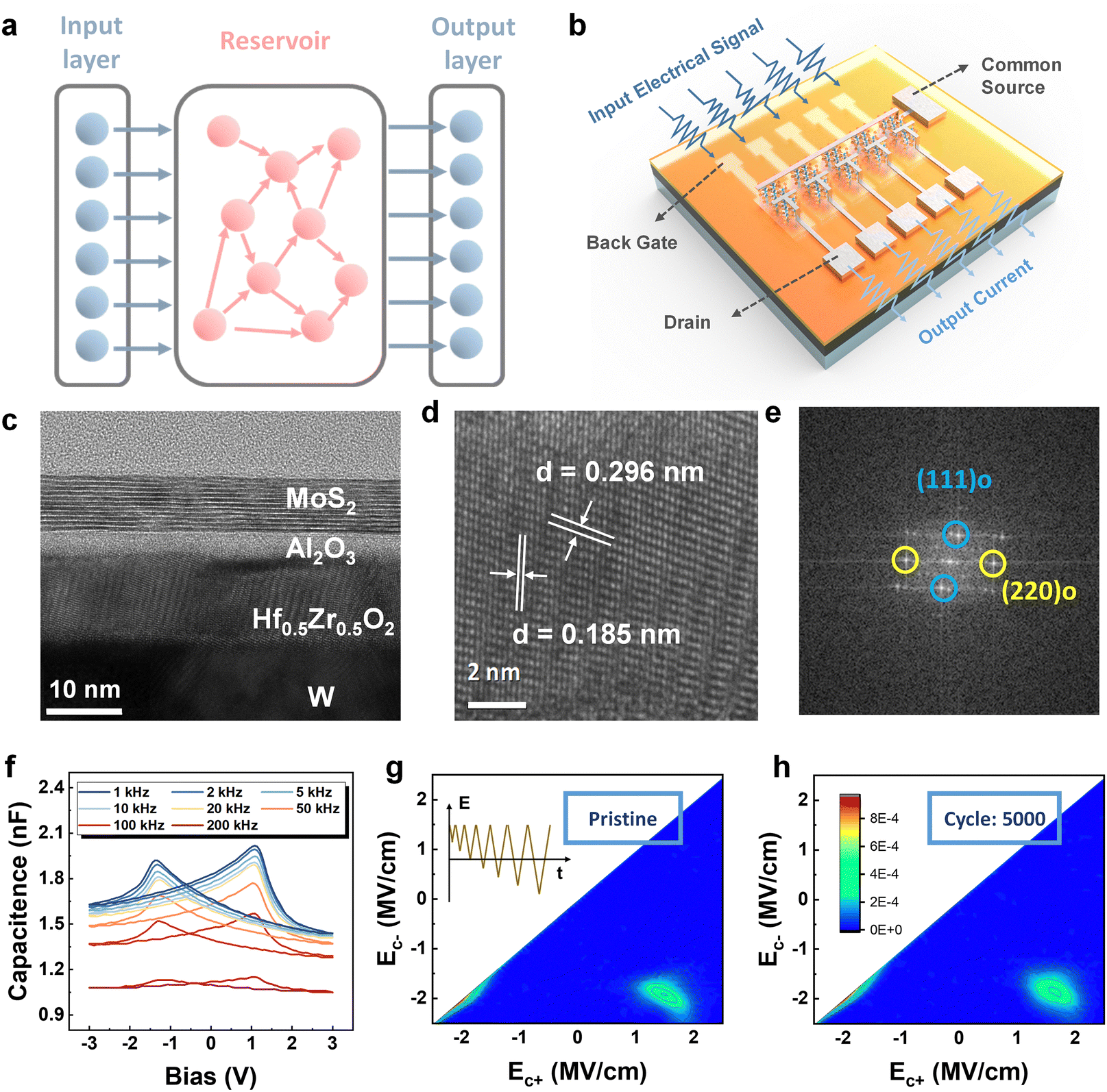 | ||
| Fig. 1 MoS2–HZO integration for reservoir computing. (a) The typical reservoir computing architecture and the correlations between input layer, reservoir, and output layers. (b) Schematic of a MoS2 HZO-based FeFET array with separated drain and gate, stimulated by electrical voltage inputs and current outputs. (c) MoS2/Al2O3/HZO/W heterostructure as shown in HRTEM cross-section image. The fast Fourier transform (FFT) analysis is carried out to indicate the HZO crystal structure, in which (d) the d-spacing of 2.96 and 1.85 Å correspond to (e) crystalline planes of (111) and (220) of the ferroelectric HZO phase, respectively. (f) The C–V characteristics of the MFM capacitor with a 10 nm HZO film are presented, ranging from 1 kHz to 200 kHz, revealing two characteristic peaks in the C–V hysteresis loop, indicative of its ferroelectric properties. Evolution of the Preisach switching density in (g) the pristine state, and (h) after 5000 cycles of external field in the HZO sample. The external field bipolar cycles used a voltage amplitude of 3 V with a frequency of 1 kHz. | ||
Physically implemented reservoirs require physical devices that are responsive to continuous pulse signals and exhibit a non-linear fading effect, which simplify computations to spatiotemporal node states.7,8 At present, memristors-based RC systems have been widely explored in various applications, such as pattern classification,9–13 spoken digit recognition,10,12,14–16 and chaotic time series prediction.7,17,18 Among these, most devices utilize ions to establish conductive channels within the dielectric for regulating resistance, yet this approach introduces variability and restricts their controllability. Compared to those based on filament formation, devices utilizing ferroelectric domain switching through voltage control, demonstrate superior voltage reliability, prolonged lifespan and accelerated operational speed. However, the destructive nature of the read/write operations and the passive characteristics of FeRAMs have limited their widespread adoption. In contrast, three-terminal ferroelectric field-effect transistors (FeFETs) offer a promising alternative. FeFETs exhibit fading memory by utilizing the polarization reversal induced by the applied gate voltage (VG) and the depolarization field when the gate voltage is removed (VG = 0 V). These ferroelectric-based three-terminal devices not only showcase active control capabilities but also exhibit reconfigurability.19,20
In this work, we utilize a two-dimensional (2D) MoS2 channel to provide excellent electrostatic control of the channel, which is integrated with an interfacial layer (Al2O3) to mitigate the random and uncontrollable interface trapping effects commonly observed in three-dimensional bulk channels.21,22 By utilizing the insufficient charge compensation-induced depolarization field between the HZO layer and the Al2O3 layer, our physical dynamic devices exhibit a remarkable non-linear fading memory characteristic. Notably, to make our devices suitable for diverse RC tasks, we fine-tune the ALD process by adjusting the O3 pulse time to modulate the oxygen vacancy concentration in HZO and influence the voltage response of the ferroelectric domain. By optimizing growth conditions, our physical RC achieves high accuracy (>95%) in Modified National Institute of Standards and Technology (MNIST) handwritten digit recognition within just 40 training epochs, highlighting the abundance of reservoir states and the device's effectiveness in handling fundamental neuromorphic tasks. Furthermore, we successfully apply the cyclic RC concept to accomplish waveform classification tasks, yielding high determination coefficients (R2) of up to 0.961 and low normalized root mean square errors (NRMSE) of 0.099. These findings underscore the potential of our proof-of-concept demonstration in reducing hardware complexity and enabling energy-efficient machine learning across a wide range of real-life time-series information processing applications.
Results and discussion
Fundamental ferroelectricity of the gate dielectric layer
An integrated array of FeFET devices based on 2D MoS2 was fabricated to demonstrate the RC concept, as schematically illustrated in Fig. 1(b). In this array, five devices with common source but separate gate and drain work together using electrical voltage inputs from the gate and current responses obtained from the source. The details of the device fabrication process can be found in the experimental section and the optical image is shown in Fig. S1 (ESI†). Fig. 1(c) shows the cross-sectional heterostructure of the proposed MoS2 HZO-based FeFETs by high-resolution transmission electron microscopy (HRTEM). Here, the gate dielectric is made of a 2![[thin space (1/6-em)]](https://www.rsc.org/images/entities/char_2009.gif) nm aluminium oxide (Al2O3) layer and a 10nm polycrystalline HZO layer while tungsten (W) is used as the gate electrode. The polar orthorhombic phase (o-phase) with (111), o-phase (220) yields a d-spacing of 2.96 and 1.85 Å, as identified in the zoomed-in TEM image (Fig. 1(d)), corresponding to the (111) and (220) planes of o-phase, respectively, as shown in the fast Fourier transform (FFT) diffraction pattern in Fig. 1(e). The consistency of these results with previous studies affirms the presence of ferroelectric phases in the HZO layer.23,24 Energy Dispersive X-ray spectroscopy (EDX) analysis is performed (Fig. S2, ESI†) to validate the chemical compositions of the MoS2–HZO integrated device.
nm aluminium oxide (Al2O3) layer and a 10nm polycrystalline HZO layer while tungsten (W) is used as the gate electrode. The polar orthorhombic phase (o-phase) with (111), o-phase (220) yields a d-spacing of 2.96 and 1.85 Å, as identified in the zoomed-in TEM image (Fig. 1(d)), corresponding to the (111) and (220) planes of o-phase, respectively, as shown in the fast Fourier transform (FFT) diffraction pattern in Fig. 1(e). The consistency of these results with previous studies affirms the presence of ferroelectric phases in the HZO layer.23,24 Energy Dispersive X-ray spectroscopy (EDX) analysis is performed (Fig. S2, ESI†) to validate the chemical compositions of the MoS2–HZO integrated device.
To examine the ferroelectric behavior, we fabricate metal–ferroelectric–metal (MFM) devices using the same HZO process conditions as our HZO-based MoS2 FeFETs. We conduct a comprehensive analysis of the capacitance–voltage (C–V) characteristics at various frequencies to examine the property of the 10-nm HZO layer. Fig. 1(f) illustrates the “butterfly” shaped C–V curves, with the two peaks of the curve corresponding to the coercive voltages (Ec) of the ferroelectric film. These observed characteristics are well-recognized indications of ferroelectric behavior.
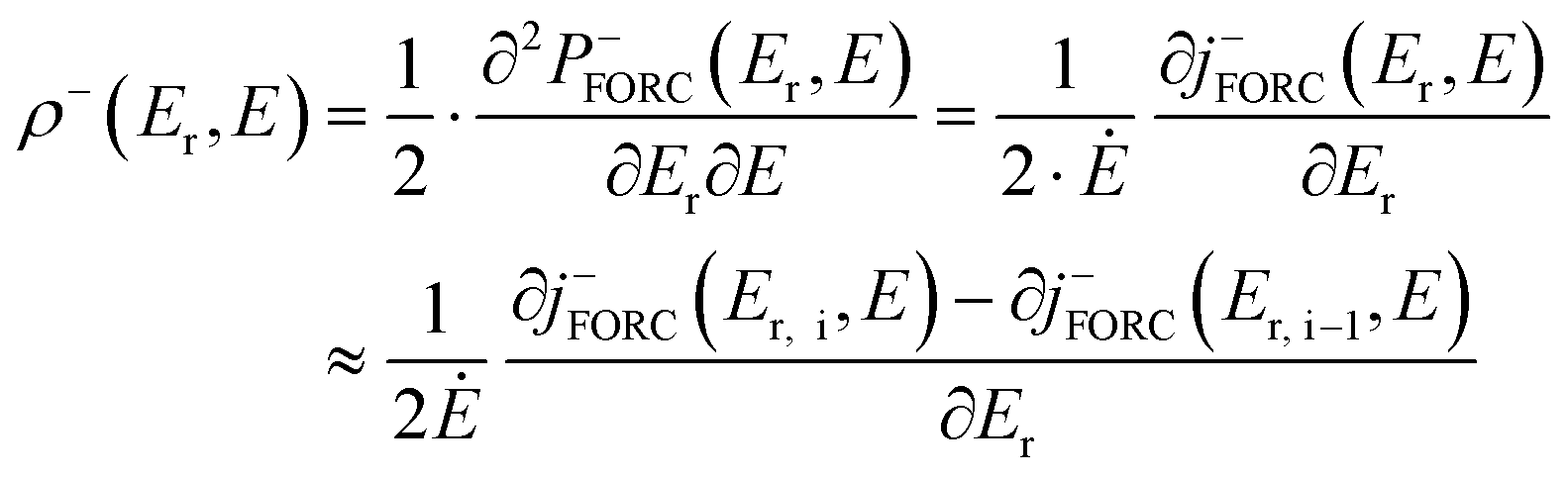
First-order reversal curve (FORC) is a robust experimental technique to analyze the switching field distributions.25,26Fig. 1(g) shows the built-in bias field and coercive field in terms of the Preisach switching density (ρ) during endurance tests. Fig. S3 (ESI†) illustrates the ρ measurement process, which initiates a positive saturated field and sweeps between the reversal field and positive saturation, irementally amplifying the magnitude of the reversal field (Er) until a negative saturation polarization is achieved. By sweeping the applied field, the polarization–electric field (P–E) curve and switching current density corresponding to each reversal field Er,i can be obtained. The switching density ρ−(Er,E) can be calculated using the following equation:25–27
 | (1) |
 | (2) |
000 times ferroelectric domain switching. In Fig. 1(h), the corresponding FORC contour plot is displayed for the sample after 5000 cycles. It can be observed that the distribution related to the built-in bias and coercive field remained largely unchanged, confirming the reliability of HZO.
Ferroelectric assisted nonlinear fading memory in FeFETs
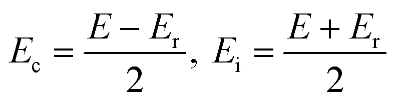
Non-linear fading memory is a crucial performance parameter for the physical implementation of RC devices, which can be deconstructed into the response process and fading memory process. In this work, we leverage the dynamics of ferroelectric domain switching to realize the response process. Initially, we focus on the MFM capacitor to observe the dynamic ferroelectric behavior. The ferroelectric switching dynamic of the 10 nm HZO layer was examined using a typical positive up negative down (PUND) scheme through the MFM capacitor.28 This scheme employs six triangular waveforms with a frequency (f) of 5 Hz to eliminate the paraelectric components. The charge difference between two consecutive opposite voltage pulses was calculated to assess the polarization reversal. The voltage sweeping range was set from 1.0 V to 3.0 V with a step of 0.2 V. The extracted polarization hysteresis loop in Fig. 2(a) highlights the distinct polarization responses to different voltages. | ||
| Fig. 2 Hybrid utilization of ferroelectric properties in MoS2 FET as the operational mechanism for reservoir computing. (a) Polarization hysteresis under varying external electric fields, illustrating the influence of the electric field on domain switching. (b) Switching kinetics depicted with NLS fitting, demonstrating the multidomain characteristics and the effects of voltage and pulse duration in the applied voltage pulse. (c) The energy band diagram of the MFIS stack related to the integration of ferroelectric response in the continuous pulse train. (d) The bi-directional ID–VG curve of MFIS-FeFET (red color) and MFMIS-FeFET (black color). The distinct memory window direction can be identified in these two different gate stacks. (e) The multi-pulsed I–V measurement was conducted in the ‘above coercive’ condition. The increasing transient I–V curves across different VG values reveal the presence of ferroelectric responses as a function of program voltage and pulse width for the devices. (f) The energy band diagram of the MFIS stack illustrates the impact of insufficient charge compensation-induced depolarization field. Current decay with time after a positive gate pulse with various programming times is shown in (g) MFIS-FeFET and (h) MFMIS-FeFET. Corresponding read-after-write results indicate a more significant depolarization field in MFIS-FeFET. (i) The power-law relaxation behavior reveals the ferroelectric depolarization in MFIS-FeFET, independent of the VP biases. The independent results confirm the existence of the depolarization field. | ||
Fig. 2(b) illustrates the time-dependent change of ΔP(t)/(2Pr) under different Vext values (from 1.08 V to 3.00 V), represented by symbols. Furthermore, the TEM image in Fig. 1(c) clearly indicates that the crystallized HZO film comprises multiple domains with distinct orientations. Therefore, the application of the nucleation-limited-switching (NLS) model is crucial to validate the observed domain switching behavior, as previously established in related studies.29,30 The solid lines in the figure depict the fitted results obtained using the NLS model. This model is described by the following formula:
 | (3) |
 | (4) |
t1 corresponds to the median logarithmic value of the distribution. One can observe that when the voltage is below the coercive voltage of the ferroelectric material, there will be a less frequent occurrence of domain switching in the minor loop. When the applied voltage is larger than the coercive voltage, the domain switching demonstrates non-linear behavior in terms of pulse width and voltage magnitude.
Furthermore, in Fig. 2(c), an energy diagram is presented to illustrate the electron accumulation behavior in an HZO-based FeFET. With a positive applied voltage, a multitude of dipoles switch, drawing more channel electrons and thereby enhancing the channel conductance, resulting in an increased current at the drain terminal. Considering that different voltage intensities or pulse widths would lead to the reversal of varying quantities of dipoles and distinct accumulations of charges in the channel, the FeFET device displays unique response characteristics when subjected to sequential input voltage pulses at the gate terminal.
Additionally, we harness the intrinsic depolarization electric field in HZO-FeFETs to facilitate the fading memory process. While HZO has demonstrated a stable polarization that can be reversed under the influence of an electric field, the scenario with FeFETs is generally more intricate. As FeFETs typically comprise a semiconductor layer, an interfacial layer, and a ferroelectric layer, insufficient charge compensation at the ferroelectric layer interface might result in a depolarization field. The introduction of such depolarizing field causes HZO to exhibit memory decay instead of long-term memory.
To confirm that the manifestation of fading memory in HZO is due to insufficient charge compensation between HZO and interfacial Al2O3, we fabricated metal-ferroelectric-insulator-semiconductor (MFIS)- and metal-ferroelectric-metal-insulator-semiconductor (MFMIS)-FeFETs using similar fabrication processes. Compared to the MFIS-FeFET, the MFMIS-FeFET employs a metal to compensate for the charge at the ferroelectric layer, thereby aiding HZO in reducing the depolarization field.23,31 We initially compared the transfer characteristics of the two structures. It is evident that the device in the MFMIS structure exhibited a counterclockwise hysteresis loop, while the device in the MFIS structure displayed a minor clockwise loop. The counter clockwise hysteresis is attributed to the polarization reversal of HZO under the influence of positive voltage, considered a characteristic behavior of FeFET,32 while the clockwise hysteresis can be attributed to the trapping dominant behavior. However, in the multipulse I–V measurements of the MFIS-FeFET, one can observe a positive ΔID when subjected to program voltage pulses with different time widths and voltage amplitudes. Note that, charge trapping induces a reduction in ΔID. Consequently, the observed positive increase in ΔID serves as compelling evidence of ferroelectric switching. When electrons are trapped within the gate dielectric, its concentration in the channel reduces, which resulted in a negative ΔID instead of a positive ΔID. Therefore, the positive window in the transfer curve of the MFIS-FeFET is attributed to the existence of a depolarization field that induces the weakened polarization reversal of the HZO. This effect is not sufficient to offset the charge trapping induced by DC measurements. The distinct transfer direction can be elucidated by the incomplete charge compensation in the MFIS-FeFET. This incomplete compensation results in the creation of a built-in potential opposite to the polarization direction (as shown in Fig. 2(f)), contributing significantly to a non-negligible depolarization field, consequently leading to retention loss.33,34
To comprehensively understand the effects induced by charge incomplete compensation, we further analyze the decrease in drain current after positive voltage programming. Fig. 2(g) and (h) show the variation of ΔID with respect to the delay time when the positive program voltage is applied in MFIS-FeFET and MFMIS-FeFET, respectively. It is apparent that the overall current change in the MFIS-FeFET is minor and rapidly decays, while the MFMIS-FeFET exhibits a significant albeit gradual decay. This phenomenon demonstrates the ability of the device to achieve fading memory behavior without the introduction of metal in the ferroelectric and interfacial layers. Furthermore, it has been reported that the depolarization induced retention loss can be well captured by the power-law equation35
 | (5) |
Effect of oxygen vacancy in enhancing adaptability
The modulation of ferroelectric polarization can adjust the conductance of the transistor channel, thereby generating abundant reservoir states. Therefore, to enhance the physical reservoir adaptability to various real-life tasks, it is crucial to optimize the HZO conditions for achieving moderate voltage and pulse durations to control the degree of polarization switching.Oxygen vacancy (VO) is an important parameter in the polarization switching kinetics of HZO which can be adjusted by the ozone pulse time during deposition. Fig. 3(a)–(c) showcase the ferroelectric domain switching behavior with variations in pulse widths and voltage amplitudes, clearly illustrating the significant influence of VO in HZO on field-dependent ferroelectric polarization switching dynamics. Fig. 3(d) demonstrates distinct switching behavior under the same voltage amplitude but varying pulse widths, extending to the response to an identical pulse train. Meanwhile, Fig. 3(e) presents diverse results under different amplitudes but a fixed pulse width of 10 μs, extending to the response to a non-identical pulse train. Both figures show a consistent trend, wherein larger ozone pulse times reflect an overall increase in switching times for polarization reversal. Shorter ozone pulse times result in a rapid ferroelectric response but also reach saturation quickly, while moderate ozone pulse times generate the most homogeneous ferroelectric response loop. This behavior is attributed to the influence of VO on phase generation in HZO.36,37
 | ||
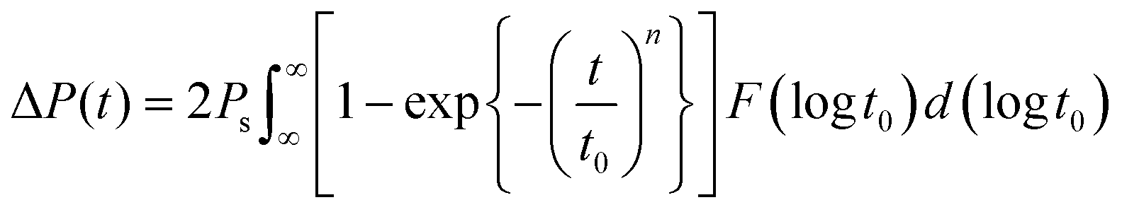
| Fig. 3 Ozone pulsing time effect on the HZO ferroelectricity. Contour maps of the ferroelectric polarization switching under various ozone pulse times (tO3) as a function of pulse voltage and pulse width: (a) tO3 = 0.1 s, (b) tO3 = 1.0 s, and (c) tO3 = 5.0 s. The switching kinetics show the impacts of voltage and duration of the applied voltage pulse. (d) Response to consecutive pulses under the same voltage of devices with different tO3 conditions. (e) Comparison of device responses to various voltages with a fixed pulse time under different tO3 conditions. (f) GIXRD spectra of HZO crystallized films were collected at an incident angle of 0.5° for devices with different ozone pulse time stacks in the 2θ range of 20°–50°. The peak centered at ∼30.4° is attributed to the mixed o (111) and t (011) planes. (g) The mixed peak position and portions, extracted from GIXRD spectra of the HZO films, vary as a function of tO3. (h) Polarization hysteresis loops of the capacitors with different tO3, alongside (i) the effect of tO3 on leakage current. The HZO condition is fixed at Tdep = 280 C and TRTA = 400 °C for the three ozone pulsing conditions. | ||
Grazing-incidence X-ray diffraction (GIXRD) measurements were conducted to analyze the various crystalline structures of the HZO layer and the relative ratios of crystalline phases within the films under different ozone pulse times, as illustrated in Fig. 3(f). The experiments were performed with an incident angle of 0.5° using Cu radiation, and the 2θ range spanned from 20° to 50°. The GIXRD patterns displayed the most prominent diffraction peaks at a 2θ value of approximately 30.4°, corresponding to the mixed reflections from the (111) planes of the o-phase or the (101) planes of the t-phase.24,38 Another distinct peak at a 2θ value of around 31.5° corresponded to the (111) planes of the m-phase. The peaks of the o (111)/t (011) and m (111) were considered as potentially involved peaks for peak splitting as the differentiation of o (111) and t (011) from GIXRD is difficult due to the overlap of the diffraction peaks. The peaks were integrated within a 2θ range of 27.5° to 33.5°. Fig. 3(g) depicted the diffraction results, and the ratio Ao-/t-phase/Ao-/t-+m-phase was calculated, with A representing the peak areal intensity fitted using Gaussian function. Moreover, a shift to lower 2θ values was generally correlated with a higher polar orthorhombic phase fraction and a reduced nonpolar tetragonal phase fraction.39 The results of the area ratio and the 2θ values of the mixed peak are shown in Fig. 3(g) for comparison. While tO3 = 0.1 s is associated with a high o-/t-phase ratio, the concentration in the mixed peak mostly comprised the t-phase. Conversely, tO3 = 5.0 s is linked to a high m-phase and a relatively high t-phase concentration compared with tO3 = 1.0 s. The observed tendency indicates that the increase in the oxygen content in the HZO film led to a higher m-phase fraction, whereas an excessive VO concentration is preferred for the t-phase stabilization. The o-phase is known to contribute to ferroelectricity, while the t-phase or m-phase does not. Additionally, when an electric field is applied to the HZO film, domains with an orthorhombic phase initially switches around pinned domains with the same polarization orientation as the direction of the applied field.40 These pinned domains served as seed domains, leading to initial switching. Consequently, the reduction in the o-phase and seed domains with increasing oxygen pulse time was suggested as the primary factor contributing to the overall increase in switching times for polarization reversal. However, the abundance of ozone vacancies, signalling insufficient polarization for effective switching, corresponds to the trend of easily saturated switching.
In Fig. 3(h), the HZO film deposited using tO3 = 1.0 s presents the highest Pr in the polarization-voltage hysteresis loops, which is attributed to the largest fraction of o-phase and less non-ferroelectric m-phase as indicated in the GIXRD results. Furthermore, the reduced defects, as suggested in Fig. 3(i), also contribute to the largest polarization. In addition, the film of tO3 = 1.0 s exhibits more than one order of magnitude lower in the leakage current than the film of tO3 = 0.1 s (Fig. 3(i)), but slightly decreased domain switching dynamic, making it suitable for subsequent device fabrication.
Demonstration of rich reservoir states in MNIST handwritten digits recognition
The achievement of a diverse range of reservoir states is a crucial factor in enhancing reservoir computing capability. In this study, we utilize the MNIST dataset to quantitatively evaluate the performance of the rich reservoir states generated by MoS2-based FeFET devices in signal processing tasks.To perform the MNIST task, a crucial requirement is that the devices must exhibit the ability to respond to a series of voltage pulses and demonstrate rich final states under different sequences, where the input pulses share the same amplitude. The key parameter for generating a sufficiently diverse reservoir state is long-term weight adjustment. Long-term potentiation (LTP) measurements are conducted to highlight the device's capability to produce a diverse reservoir state after a pulse train as shown in Fig. 4(b). Following each program pulse, a read voltage (Vread) of 0 V with VD = 0.5 V is applied to measure transient conductance. Specifically, when the channel current induced by the first pulse cannot fully relax to the initial state, the arrival of the second pulse results in a higher current response, indicating an accumulation effect. The observed fading memory properties, as discussed in Fig. 2(g), play a crucial role in the spatiotemporal dynamics of our HZO-based FeFETs. These properties lead to the generation of a non-linear accumulation value after each pulse in the train, ultimately producing a distinct final conductance state.
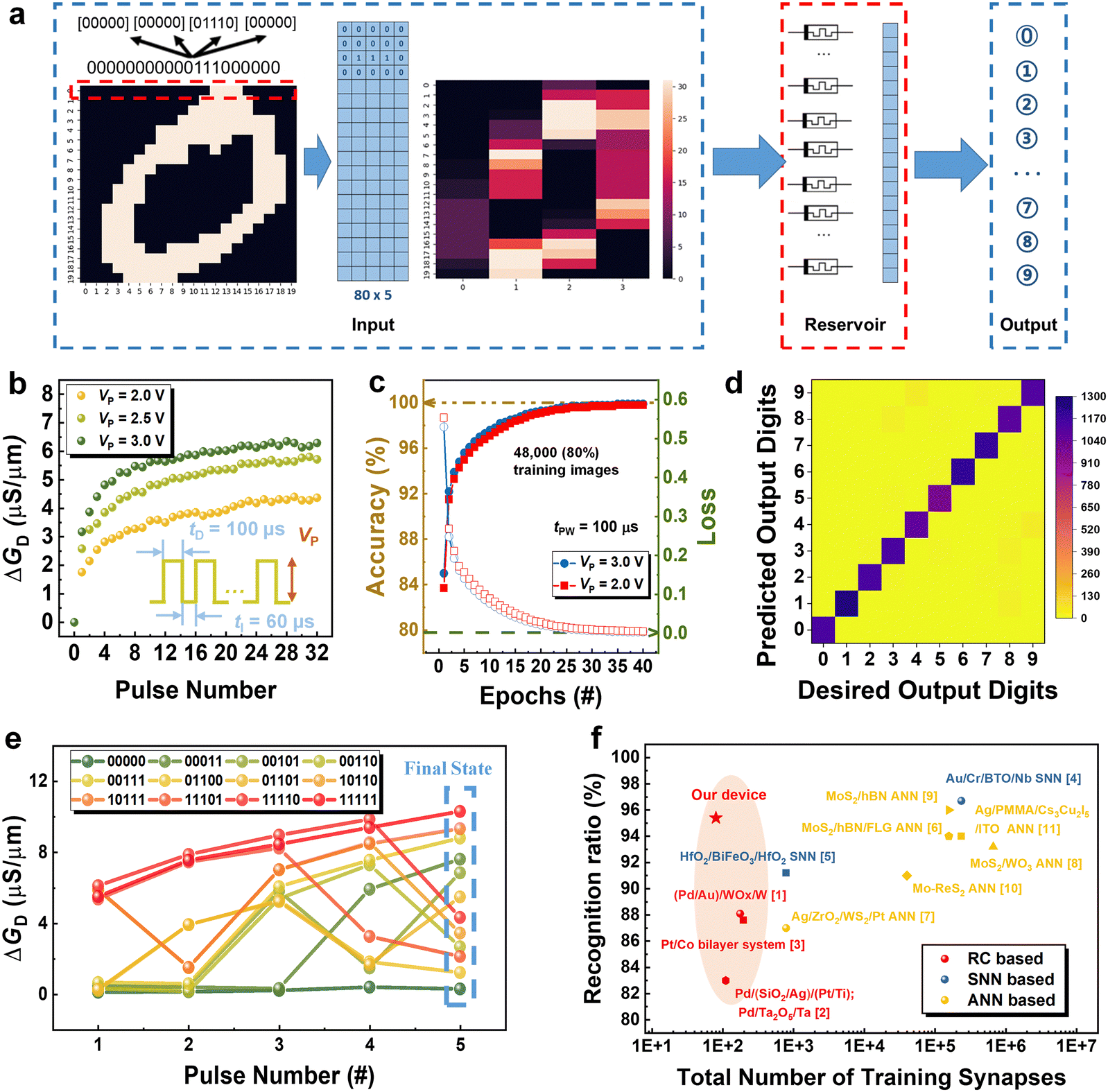 | ||
| Fig. 4 Physical reservoir computing system for MNIST database recognition task. (a) Process flow of MNIST classification, using the digit ‘0’ as an example. The original digit image was pre-processed to minimize the input count. Five temporal signals were grouped to represent five pixels, and each row (20 pixels) comprised 4 signal groups transferred into one device. (b) Modulation of conductance states was achieved using a positive sequential discrete VG pulse stream. All input pulse trains had a fixed tPW of 100 μs, with an identical programming biases (VP) of 2.0 V, 2.5 V and 3.0 V. Post-synaptic conductance was measured with VD set to 0.5 V. (c) Variation of accuracy (solid line) and loss (hollow line) depicted during the iterative training process. Accuracy reached 100% after 30 epochs, and the loss decreased to nearly 0. (d) A matching confusion matrix was recorded during the testing process with a total of 1200 images, showing recognition accuracy of up to 95.43%. (e) Conductance states modulated by 12 different VG pulse trains: (00000, 00011, 00101, 00110, 00111, 01100, 01101, 10110, 10111, 11101, 11110, 11111). (f) Benchmarking comparison with other neural network-based devices under the same MNIST classification tasks. | ||
Due to the inadequate responsiveness difference of the device to continuous pulses, we perform a pre-processing of the original images, as shown in Fig. 4(a). Taking a digit ‘0’ image as an example, we first binarize and crop the original 28 × 28 grayscale image to obtain a 20 × 20 image with 20 pixels per row. We then remove the unused border area and set the grayscale values below 80 to ‘0’ and those above 80 to ‘1’. Subsequently, each row is divided into smaller sections by combining five pixels into one which converts the 20 × 20 image into 20 × 4 matrix. Note that each pixel in the 20 × 4 matrix represents one conductance state. These conductance values are fed to reservoir and served as an individual reservoir node, which is linked to others in the same rows to form a high-dimensional input vector Xi for software training. The algorithm for training is a simple logistic regression with sigmoid function as follows:
 | (6) |
By using this method, we convert 60000 images in MNIST database to conductance matrix. Herein, the 32 different pulse streams contain 5 consecutive binary signals (e.g., 00011), where the pulse width and interval are 100 μs and 60 μs, respectively. Given a series of five continuous binary signals and only one final conductance value is considered, there are a total of 32 possible conductance states for the reservoir. The training information, comprising of 48000 digit images (80% of the database), are then fed into the readout layer to obtain the weight matrix (Wout). It is crucial to note that the structure facilitating communication between the reservoir and the output layer is a fully connected layer. After Wout is formed, the rest of dataset consisting of 12000 images are used to test the recognition accuracy.
In order to provide a clear illustration, we have selected 12 representative states to depict their responses to different temporal inputs as shown in Fig. 4(e). One can observe that each input signal has a unique output conductance such that the device can be used to separate different inputs. Fig. 4(c) demonstrates that the training accuracy reached 100%, and the loss decreased to 0 after 30 epochs using 48000 training images (80% of the dataset). It is important to note that the training loss and accuracy were determined by sparse categorical cross entropy and accuracy, respectively. Fig. 4(d) illustrates that the testing accuracy for 12000 images reached 95.43% using a pulse train with a pulse amplitude of 3 V and a pulse time of 100 μs.
Fig. 4(f) shows the benchmarking of MNIST classification task using not only RC but also other neural network-based devices based on 2D materials or ferroelectric materials.7,10,11,41–47 Our devices show rich reservoir states to deal with the task and superior performance with less training cost, which are attributed to the minimized network size.
Unveiling high-dimensional mapping capacity via waveform classification using cyclic RC
Fig. 5(a) shows the cyclic RC architecture. The variant of RC model was proposed to improve the high-dimensional mapping ability, which uses time multiplexing mask process to generate more reservoir states in the time domain. Here, the delay systems with rich dynamical properties show the benefits for processing time-dependent signals.14 First, the given input signals are pre-processed by multiplying them with a randomly generated mask, which is a one-dimensional vector consisting of only −1 and 1 element, resulting in a time-dependent input stream. Subsequently, the amplitude of the input matrix is linearly mapped to voltage range proportional to the endurance electric field of our transistor. And then the resulting voltage values are converted to a train of voltage pulses through a signal generation system. Note that, in this time-multiplexing process, the mask length (M), which represents the number of intervals in the delay loop, is determined by the total number of elements in the binary matrix. The number of masks (N) represents the number of reservoirs in parallel. The input voltage stream for each reservoir is then applied to our FeFET, recording M reservoir nodes that are sequentially connected in a delay loop with a fixed duration time, τ (set at 120 μs). Accordingly, the output reservoir states in the virtual nodes can be linearly combined (e.g., M = 2 and N = 2, which means each signal is time-multiplexed using two matrices, each with a length of 2, respectively.) and then served as input Xi to regress output Yi. SoftMax regression is used as an algorithm for readout function, as we explained at the last section (the details shown in Datasets and readout function model section). Notably, the output layer is fully connected with the reservoir layer in this task, ultimately yielding the output results.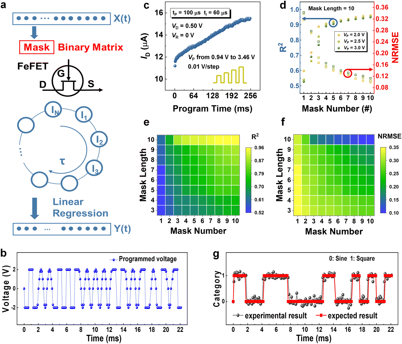 | ||
| Fig. 5 Waveform classification realized with dynamic RC system. (a) Schematic of the dynamic RC system demonstrated on integrated MoS2–HZO based FeFETs. Before a given input vector is transformed into the system, a binary mask containing ‘−1’ and ‘1’ elements were used to process the signal to increase the number of virtual nodes. The entire response under the mask occurs within a duration time τ. Linear regression model is used to get the weights (Wout) and the output vector is a linear combination of the virtual nodes. (b) The input sequence was a random combination of sine and square waveforms and transferred into the devices by discrete voltage. (c) The modulation of conductance states with the pulse train demonstrates the device's capability to respond to a series of non-identical amplitude pulse trains. Non-identical programming bias (VP) was introduced from 0.94 V to 3.46 V at 0.01 V per step. The fixed programming time (tP) of 100 μs was applied to all the input pulse trains, with an interval time (tI) of 60 μs. The read voltage (Vread) of 0 V with VD = 0.5 V was set to measure the post-synaptic conductance. (d) Variation of R2 and NRMSE as a function of the number of paralleled reservoirs under different programmed voltage. The contour maps show variation of (e) R2 and (f) NRMSE with respect to mask number and mask length. (g) The classification results of waveforms were obtained using 10 masks, each with a mask length set to 10. The desired output was a binary sequence consisting of ‘0’ and ‘1’, representing sine and square waveforms, respectively. | ||
When addressing temporal information, the utilization of a binary mask enhances cyclic RC capability through time multiplexing. Simultaneously, it elevates the demand for physical devices to generate varied responses to distinct input voltage amplitudes. A pulse train, encompassing non-identical pulse amplitudes, is applied to our device to assess its response. The pulse width is consistently set to 100 μs, and VD remains fixed at 0.5 V. The pulse amplitudes range from 0.94 to 3.46 V in increments of 0.1 V. The non-linear behavior depicted in Fig. 5(c) underscores the remarkable capability of our device in effectively handling pulse trains with varying amplitudes.
A benchmark waveform classification task is carried out to further evaluate the time-series signal performance of the FeFET-based RC system. Two parameters, R2 and NRMSE, are used to quantify the performance. An R2 value close to 1 indicates that the experimental results fit well with the expected results. NRMSE is used to measure the classification error, which is described as:14,48
 | (7) |
As exhibited in Fig. 5(b), the original input signal is a random combination of sine and square waves, and the purpose of the task is to use ‘0’ and ‘1’ to represent square and sine waves, respectively.
The optimal classification results are dependent on the number of parallel masks (N) and programmed voltage (VP) as elucidated in Fig. 5(d), with a fixed mask length (M) of 10. The programmed voltage is a constant derived from the multiplication of a binary matrix by a scaling factor, effectively augmenting the values within the matrix. Specifically, when VP is set to 2 V, the matrix elements assume the values of ‘−2’ and ‘2’. We aggregate masks in parallel as a unified entity to preprocess a consistent input signal with varying programmed voltages. It is noteworthy that each mask within the group is unique, yet those applied to different voltages remain consistent. Observations within the VP range of 2 V to 3 V unveil a notable trend: an increase in mask number corresponds to a simultaneous reduction in error rate R2 and an increase in NRMSE. Additionally, for specific N, a distinct pattern emerges wherein an elevation in VP results in a low R2 and a large NRMSE. This dependence is attributed to the system's fundamental capability in handling continuous signals. In other words, the overall change in Fe-FET conductance is constrained, and excessive VP can drive reservoir states to the upper limit, compromising further signal processing capabilities in subsequent durations.
Apart from the number of N and VP, M is a critical parameter. Here, the length of the mask matrix represents the number of virtual nodes, reflecting the state richness of the RC system determined by the binary combinations of the mask sequence. Consequently, we delve into the performance dependence of these two parameters, fixing VP at 2 V for comparison. The waveform classification task presents a notable challenge to the system when either a single mask is applied, or the length of each mask is only one. Expectedly, with the increase in values of N and M, we observe a significant improvement in R2, rising from the lowest value of 0.523 to a high accuracy value of 0.961 in Fig. 5(e). Simultaneously, NRMSE, depicted in Fig. 5(f), decreases to an exceptionally low value of 0.099. The optimal classification results, represented by the gray set points, for the three parameters mentioned above are illustrated in Fig. 5(g) with VP set to 2 V, M fixed at 10, and N at 10. The red set showcases the expected results, where ‘0’ and ‘1’ denote square and sine waves, respectively.
Conclusions
In conclusion, we have successfully demonstrated a high-performance MoS2–HZO integrated FeFET, highlighting its efficacy in processing intricate real-life time-series information. Our strategic modifications to the device structure induced insufficient charge compensation, thereby amplifying the depolarization electric field to achieve the volatile memory phenomenon. Further fine-tuning of the ferroelectric switching behavior is accomplished by adjusting the ozone pulse time during ALD deposition, allowing for the adaptability of different RC systems. The effectiveness of our proposed device is substantiated by its ability to maintain adequate reservoir states while ensuring energy efficiency, as validated through the MNIST handwritten recognition task. Moreover, our devices exhibit exceptional performance in waveform classification tasks based on a cyclic RC system, achieving an impressive R2 value of up to 0.961. This proof-of-concept demonstration not only manifests the potential of utilizing FeFETs in energy-efficient machine learning but also enables broader applications in artificial intelligence.Experimental
Ferroelectric metal-ferroelectric-metal (MFM) capacitors Preparation
A 30 nm W layer is deposited on the silicon oxide substrate by sputter. Then a ∼10 nm HZO layer is deposited using ALD with ozone pulsing time (tO3) of 1 s and deposition temperature (Tdep) of 280 °C. We select Hf and Zr metals sources using the Hf[N–(C2H5) CH3]4 and Zr[N–(C2H5) CH3]4 precursors with N2 carrier gas flow rate of 250 sccm. The Hf and Zr sources pulse time are 2.0 s and 1.6 s, respectively, with a fixed N2 purge time of 15 s. In addition, the ozone precursor was mixed with the N2 carrier gas with a constant flow rate of 100 sccm followed by the 30 s purge time. Ellipsometry is used to confirm the thickness of HZO layer, in which the growth rate is found to be ∼1 Å per cycle. To activate the ferroelectricity, a 60 s rapid thermal annealing process is conducted at 400 °C after sputtering a 30 nm of tungsten sacrificial layer.Finally, top W electrodes is deposited and an area of 100 × 100 μm2 are defined using the optical lithography. Subsequently, standard commercial tungsten etchant is used to do the wet etch.
Transistor fabrication
First, we sputtered a 30 nm W layer on the silicon oxide substrate and then defined the back gate pattern by laser writer and wet etch. Following, a HZO layer is deposited and activated using a process flow identical to the MFM process. The Al2O3 interfacial layer (IL) is deposited using atomic layer deposition (ALD) process at a low Tdep of 150 °C to mitigate the charge carrier interaction with the intrinsic defects in IL, thereby improving the interface quality. For MFIS-FeFETs, the W layer is removed using a standard commercial W etchant. Subsequently, 2 nm of Al2O3 is deposited. In contrast, for MFMIS-FeFETs, a 6 nm Al2O3 layer is deposited after patterning the W layer. Next, multilayer-MoS2 flakes are mechanically exfoliated and transferred using a designated transfer stage. Subsequently, the S/D contacts are defined by electron-beam lithography with a fixed LSD = 1 μm, Lch = 1 μm and Wch = 5 μm, followed by the lift-off process with 25 nm of Ni deposited using an electron beam evaporator. To minimize the bombardment damage on the MoS2 top surface, a low Ni deposition rate of 0.1 Å s−1 is selected. To further reduce the stray current, we use Ar/SF6 to isolate each device in the array by inductively coupled plasma (ICP) etching. The etching time is 10 second and N2 is used as the carrier gas. In the array, the S/D contacts are defined with a fixed LSD = 1 μm, Lch = 1 μm and Wch = 1 μm.Electrical characterization and parameter extraction
The electrical characterizations, including DC I–V, pulsed I–V, and PUND measurements, were done using a Keysight B1500A semiconductor analyzer under the dark ambient environment at room temperature. The polarization hysteresis loops are derived using a typical PUND scheme, involving six triangular waveforms with a frequency of 5 Hz, aimed at subtracting the paraelectric counterparts.Datasets and readout function model
The Mixed National Institute of Standards and Technology (MNIST) database was widely used for training and testing in machine learning research. The database contained 60000 training images and 10000 testing images (sized 28 × 28 pixels) representing digits written by high-school students and employees of the United States Census Bureau.
The training algorithm employed is a logistic regression (LR) known as Scikit-learn package which can be found in Python program. All root means square errors were calculated by sklearn. metrics () tool in the package.
Author contributions
L. L., H. X. and Y.-C. C. designed the experiments. L. L., H. X. and H. Z. performed the experiments. L. L., H. X., Y.-C. C., N. D. and J. G. conducted the device measurement. L. L. wrote the original manuscript. H. X. and K.-W. A. revised the manuscript. K.-W. A. supervised the work. All authors commented the manuscript.Conflicts of interest
There are no conflicts to declare.Acknowledgements
This research is supported by A*STAR Science and Engineering Research Council (A2083c0061), National Research Foundation, Singapore (NRF-CRP22-2019-0007, NRF-CRP24-2020-0002), Ministry of Education Tier-1 and Tier-2 Grant (MOE-T2EP50120-0016). Y.-C. C. acknowledges Applied Materials-NUS Advanced Corporate Laboratory Scholarship (A*STAR IAF-ICP I1801E0022).References
- Y. LeCun, Y. Bengio and G. Hinton, Nature, 2015, 521, 436–444 CrossRef CAS PubMed.
- X. Feng, S. Li, S. L. Wong, S. Tong, L. Chen, P. Zhang, L. Wang, X. Fong, D. Chi and K.-W. Ang, ACS Nano, 2021, 15, 1764–1774 CrossRef CAS PubMed.
- L. Guo, N. Li, F. Jia, Y. Lei and J. Lin, Neurocomputing, 2017, 240, 98–109 CrossRef.
- J. Zhu, Q. Jiang, Y. Shen, C. Qian, F. Xu and Q. Zhu, J. Mech. Sci. Technol., 2022, 36, 527–542 CrossRef.
- S. Hochreiter and J. Schmidhuber, Neural Comput., 1997, 9, 1735–1780 CrossRef CAS PubMed.
- W. Maass, T. Natschläger and H. Markram, Neural Comput., 2002, 14, 2531–2560 CrossRef PubMed.
- C. Du, F. Cai, M. A. Zidan, W. Ma, S. H. Lee and W. D. Lu, Nat. Commun., 2017, 8, 2204 CrossRef PubMed.
- Y. K. Chembo, Chaos, 2020, 30, 013111 CrossRef PubMed.
- L. Sun, Z. Wang, J. Jiang, Y. Kim, B. Joo, S. Zheng, S. Lee, W. J. Yu, B.-S. Kong and H. Yang, Sci. Adv., 2021, 7, eabg1455 CrossRef CAS PubMed.
- W. Jiang, L. Chen, K. Zhou, L. Li, Q. Fu, Y. Du and R. H. Liu, Appl. Phys. Lett., 2019, 115, 192403 CrossRef.
- R. Midya, Z. Wang, S. Asapu, X. Zhang, M. Rao, W. Song, Y. Zhuo, N. Upadhyay, Q. Xia and J. J. Yang, Adv. Intell. Syst., 2019, 1, 1900084 CrossRef.
- M. Pei, Y. Zhu, S. Liu, H. Cui, Y. Li, Y. Yan, Y. Li, C. Wan and Q. Wan, Adv. Mater., 2023, 35, 2305609 CrossRef CAS PubMed.
- Y. Yang, H. Cui, S. Ke, M. Pei, K. Shi, C. Wan and Q. Wan, Appl. Phys. Lett., 2023, 122, 043508 CrossRef CAS.
- Y. Zhong, J. Tang, X. Li, B. Gao, H. Qian and H. Wu, Nat. Commun., 2021, 12, 408 CrossRef CAS PubMed.
- J. Moon, W. Ma, J. H. Shin, F. Cai, C. Du, S. H. Lee and W. D. Lu, Nat. Electron., 2019, 2, 480–487 CrossRef.
- D. Verstraeten, B. Schrauwen and D. Stroobandt, in The 2006 IEEE International Joint Conference on Neural Network Proceedings, 2006, pp. 1050–1053.
- H. Jaeger, NIPS.
- J. Pathak, B. Hunt, M. Girvan, Z. Lu and E. Ott, Phys. Rev. Lett., 2018, 120, 024102 CrossRef CAS PubMed.
- S. Dutta, B. Grisafe, C. Frentzel, Z. Enciso, M. S. Jose, J. Smith, K. Ni, S. Joshi and S. Datta, IEEE Trans. Electron Devices, 2021, 68, 516–522 CAS.
- J. Muller, T. S. Boscke, U. Schroder, R. Hoffmann, T. Mikolajick and L. Frey, IEEE Electron Device Lett., 2012, 33, 185–187 Search PubMed.
- M. Si, C.-J. Su, C. Jiang, N. J. Conrad, H. Zhou, K. D. Maize, G. Qiu, C.-T. Wu, A. Shakouri, M. A. Alam and P. D. Ye, Nat. Nanotechnol., 2018, 13, 24–28 CrossRef CAS PubMed.
- Y.-C. Chien, H. Xiang, Y. Shi, N. T. Duong, S. Li and K.-W. Ang, Adv. Mater., 2023, 35, 2204949 CrossRef CAS PubMed.
- H. Xiang, Y.-C. Chien, L. Li, H. Zheng, S. Li, N. T. Duong, Y. Shi and K.-W. Ang, Adv. Funct. Mater., 2023, 33, 2304657 CrossRef CAS.
- S. S. Cheema, D. Kwon, N. Shanker, R. dos Reis, S.-L. Hsu, J. Xiao, H. Zhang, R. Wagner, A. Datar, M. R. McCarter, C. R. Serrao, A. K. Yadav, G. Karbasian, C.-H. Hsu, A. J. Tan, L.-C. Wang, V. Thakare, X. Zhang, A. Mehta, E. Karapetrova, R. V. Chopdekar, P. Shafer, E. Arenholz, C. Hu, R. Proksch, R. Ramesh, J. Ciston and S. Salahuddin, Nature, 2020, 580, 478–482 CrossRef CAS PubMed.
- T. Schenk, M. Hoffmann, J. Ocker, M. Pešić, T. Mikolajick and U. Schroeder, ACS Appl. Mater. Interfaces, 2015, 7, 20224–20233 CrossRef CAS PubMed.
- M. Pešić, F. P. G. Fengler, L. Larcher, A. Padovani, T. Schenk, E. D. Grimley, X. Sang, J. M. LeBeau, S. Slesazeck, U. Schroeder and T. Mikolajick, Adv. Funct. Mater., 2016, 26, 4601–4612 CrossRef.
- M. Hoffmann, T. Schenk, M. Pešić, U. Schroeder and T. Mikolajick, Appl. Phys. Lett., 2017, 111, 182902 CrossRef.
- S. Mueller, J. Müller, R. Hoffmann, E. Yurchuk, T. Schlösser, R. Boschke, J. Paul, M. Goldbach, T. Herrmann, A. Zaka, U. Schröder and T. Mikolajick, IEEE Trans. Electron Devices, 2013, 60, 4199–4205 CAS.
- N. Gong, X. Sun, H. Jiang, K. S. Chang-Liao, Q. Xia and T. P. Ma, Appl. Phys. Lett., 2018, 112, 262903 CrossRef.
- A. K. Tagantsev, I. Stolichnov, N. Setter, J. S. Cross and M. Tsukada, Phys. Rev. B, 2002, 66, 214109 CrossRef.
- C. Jiang, M. Si, R. Liang, J. Xu, P. D. Ye and M. A. Alam, IEEE J. Electron Devices Soc., 2018, 6, 189–194 CAS.
- M. Si, A. K. Saha, S. Gao, G. Qiu, J. Qin, Y. Duan, J. Jian, C. Niu, H. Wang, W. Wu, S. K. Gupta and P. D. Ye, Nat. Electron., 2019, 2, 580–586 CrossRef CAS.
- T. P. Ma and J.-P. Han, IEEE Electron Device Lett., 2002, 23, 386–388 CAS.
- C. T. Black, C. Farrell and T. J. Licata, Appl. Phys. Lett., 1997, 71, 2041–2043 CrossRef CAS.
- B. S. Kang, J.-G. Yoon, T. W. Noh, T. K. Song, S. Seo, Y. K. Lee and J. K. Lee, Appl. Phys. Lett., 2003, 82, 248–250 CrossRef CAS.
- T. Mittmann, M. Materano, S.-C. Chang, I. Karpov, T. Mikolajick and U. Schroeder, in 2020 IEEE International Electron Devices Meeting (IEDM), 2020, p. 18.4.1-18.4.4.
- Comparative studies on ferroelectric switching kinetics of sputtered Hf0.5Zr0.5O2 thin films with variations in film thickness and crystallinity|Journal of Applied Physics|AIP Publishing, https://pubs-aip-org.libproxy1.nus.edu.sg/aip/jap/article/128/7/074102/347554/Comparative-studies-on-ferroelectric-switching, (accessed November 12, 2023).
- J. Wan, X. Chen, L. Ji, Z. Tu, H. Wu and C. Liu, IEEE Trans. Electron Devices, 2022, 69, 1805–1810 CAS.
- M. Hyuk Park, H. Joon Kim, Y. Jin Kim, W. Lee, T. Moon and C. Seong Hwang, Appl. Phys. Lett., 2013, 102, 242905 CrossRef.
- A. Chouprik, S. Zakharchenko, M. Spiridonov, S. Zarubin, A. Chernikova, R. Kirtaev, P. Buragohain, A. Gruverman, A. Zenkevich and D. Negrov, ACS Appl. Mater. Interfaces, 2018, 10, 8818–8826 CrossRef CAS PubMed.
- S.-T. Yang, X.-Y. Li, T.-L. Yu, J. Wang, H. Fang, F. Nie, B. He, L. Zhao, W.-M. Lü, S.-S. Yan, A. Nogaret, G. Liu and L.-M. Zheng, Adv. Funct. Mater., 2022, 32, 2202366 CrossRef CAS.
- Z. Peng, F. Wu, L. Jiang, G. Cao, B. Jiang, G. Cheng, S. Ke, K.-C. Chang, L. Li and C. Ye, Adv. Funct. Mater., 2021, 31, 2107131 CrossRef CAS.
- J. Tang, C. He, J. Tang, K. Yue, Q. Zhang, Y. Liu, Q. Wang, S. Wang, N. Li, C. Shen, Y. Zhao, J. Liu, J. Yuan, Z. Wei, J. Li, K. Watanabe, T. Taniguchi, D. Shang, S. Wang, W. Yang, R. Yang, D. Shi and G. Zhang, Adv. Funct. Mater., 2021, 31, 2011083 CrossRef CAS.
- X. Yan, C. Qin, C. Lu, J. Zhao, R. Zhao, D. Ren, Z. Zhou, H. Wang, J. Wang, L. Zhang, X. Li, Y. Pei, G. Wang, Q. Zhao, K. Wang, Z. Xiao and H. Li, ACS Appl. Mater. Interfaces, 2019, 11, 48029–48038 CrossRef CAS PubMed.
- F. Zeng, Y. Guo, W. Hu, Y. Tan, X. Zhang, J. Feng and X. Tang, ACS Appl. Mater. Interfaces, 2020, 12, 23094–23101 CrossRef CAS PubMed.
- M. E. Pam, S. Li, T. Su, Y.-C. Chien, Y. Li, Y. S. Ang and K.-W. Ang, Adv. Mater., 2022, 34, 2202722 CrossRef CAS PubMed.
- X. Zhang, J. Wang, Y. Sui, F. Wei, J. Qi, Q. Meng, Y. He and D. Zhuang, ACS Appl. Nano Mater., 2020, 3, 11945–11954 CrossRef CAS.
- A. Rodan and P. Tino, IEEE Trans. Neural Netw., 2011, 22, 131–144 Search PubMed.
Footnotes |
| † Electronic supplementary information (ESI) available. See DOI: https://doi.org/10.1039/d3nh00524k |
| ‡ L. L. and H. X. contributed equally to this work. |
| This journal is © The Royal Society of Chemistry 2024 |