
Contact engineering for 2D Janus MoSSe/metal junctions†
Yu
Shu
a,
Ting
Li
a,
Naihua
Miao
b,
Jian
Gou
c,
Xiaochun
Huang
*d,
Zhou
Cui
a,
Rui
Xiong
a,
Cuilian
Wen
 a,
Jian
Zhou
b,
Baisheng
Sa
*a and
Zhimei
Sun
*b
a,
Jian
Zhou
b,
Baisheng
Sa
*a and
Zhimei
Sun
*b
aMultiscale Computational Materials Facility, College of Materials Science and Engineering, Fuzhou University, Fuzhou 350108, P. R. China. E-mail: bssa@fzu.edu.cn
bSchool of Materials Science and Engineering, Beihang University, Beijing 100191, P. R. China. E-mail: zmsun@buaa.edu.cn
cSchool of Physics, Zhejiang University, Hangzhou 310058, P. R. China
dDepartment of Physics, University of Hamburg, D-20355 Hamburg, Germany. E-mail: huangxiaochun0321@gmail.com
First published on 16th November 2023
Abstract
The flourish of two-dimensional (2D) materials provides a versatile platform for building high-performance electronic devices in the atomic thickness regime. However, the presence of the high Schottky barrier at the interface between the metal electrode and the 2D semiconductors, which dominates the injection and transport efficiency of carriers, always limits their practical applications. Herein, we show that the Schottky barrier can be controllably lifted in the heterostructure consisting of Janus MoSSe and 2D vdW metals by different means. Based on density functional theory calculations and machine learning modelings, we studied the electrical contact between semiconducting monolayer MoSSe and various metallic 2D materials, where a crossover from Schottky to Ohmic/quasi-Ohmic contact is realized. We demonstrated that the band alignment at the interface of the investigated metal-semiconductor junctions (MSJs) deviates from the ideal Schottky–Mott limit because of the Fermi-level pinning effects induced by the interface dipoles. Besides, the effect of the thickness and applied biaxial strain of MoSSe on the electronic structure of the junctions are explored and found to be powerful tuning knobs for electrical contact engineering. It is highlighted that using the sure-independence-screening-and-sparsifying-operator machine learning method, a general descriptor WM3/exp(Dint) was developed, which enables the prediction of the Schottky barrier height for different MoSSe-based MSJ. These results provide valuable theoretical guidance for realizing ideal Ohmic contacts in electronic devices based on the Janus MoSSe semiconductors.
New conceptsAs transistor dimensions continue to shrink, achieving efficient electrical contacts in semiconductor devices becomes increasingly important. Two-dimensional (2D) materials have atomic thickness and no dangling bonds on the surface, making them the core materials for next-generation electronic devices. Furthermore, the interface formed by the 2D metal and 2D semiconductor can effectively alleviate the Fermi-level pinning (FLP) effects. Therefore, it is necessary to conduct research on the characteristics of metal-semiconductor interfaces and precisely regulate the Schottky barrier to develop ideal metal-semiconductor junctions (MSJs). Herein, we achieved Ohmic contact and controllable Schottky barrier by selecting 2D metals with different work functions together with monolayer MoSSe, an important 2D Janus transition metal dichalcogenide. It is proved that the existence of interface dipole is the main reason for the FLP effects. Furthermore, we modulate the interface properties of 2D MSJs by varying the thickness and applied biaxial strain. Finally, we developed a universal descriptor capable of predicting the Schottky barrier heights of different 2D MSJs using the machine learning method. Our study provides a new strategy for the understanding and realization of ideal electrical contacts in 2D materials-based MSJs. |
1. Introduction
Transition metal dichalcogenide (TMD) monolayers with extraordinary electronic and optoelectronic properties have great potential for next-generation silicon-beyond devices.1–4 All TMD monolayers comprise three stacked atomic-layers with the stacking configurations of X–M–X, where M is a transition metal and X is a chalcogen.4 Janus TMDs is a special class of TMDs in which the uppermost and lowermost layers of the sandwich structure consist of different chalcogen elements with stacking configurations of X–M–Y, where X and Y indicate different dichalcogenide elements.5 The broken mirror symmetry in Janus TMDs generates an intrinsic dipole moment along the vertical direction, leading to novel physical properties, such as second-harmonic generation response, enhanced in-plane piezoelectric polarization, and great catalytic performance.6,7 Monolayer MoSSe is a typical Janus TMD material that has been experimentally synthesized since 2017.8 Theoretical studies have shown that monolayer MoSSe has a tunable direct-bandgap and a high carrier mobility, possessing a potential application in atomically-thin advanced electronic devices.5,9It is known that when the size of the devices is reduced to the atomic scale, the interfacial electronic structure between the two-dimensional (2D) semiconductor and the electrode materials becomes critical in realizing high-performance applications.10,11 In particular, the energy barrier of the metal-semiconductor junctions (MSJs), namely, the Schottky barrier, limits the carrier injection and the contact-resistance characteristics of the devices.12–14 In general, the Schottky barrier is induced by two main reasons: (1) the energy difference in the work functions between the semiconductor and the electrode materials and (2) the strong Fermi level pinning (FLP) effect at the interface of the junction.15–17 To overcome this issue, proper metals need to be screened out for electrode materials. In contrast to traditional 3D bulk metals, metallic 2D materials enable the fabrication of van der Waals (vdW)-type heterojunction devices, where the FLP effect can be significantly suppressed.18–21 Thereinto, 2D metallic TMDs and 2D transition metal carbides/nitrides (MXenes) show excellent mechanical stability and electrical conductivity, making them ideal electrodes for various electronic devices and electrochemical systems.4,22,23 With the emergence of new synthesis methods for MXenes, their surface functional groups now encompass a rich chemical diversity, evolving from the initial F, O, and OH to include Cl, Br, and I.24,25 These diverse functional groups offer tunable work functions and variable 2D lattices, making MXenes potential candidates for 2D electrodes.
In this work, using first-principles calculations, we studied the interfacial contacting properties of the devices built from monolayer MoSSe and various 2D metals MXenes (Nb2C and Nb3C2 including functional group of F, O, OH) and MX2 (M = V, Nb, Ta; X = S, Se). The calculated band structures of these devices show that transition from Schottky contact to Ohmic contact can be achieved by selecting 2D metals with different work functions. We demonstrated that the presence of interface dipoles results in the FLP effect, leading to a deviation of the band alignment from the prediction of the ideal Schottky–Mott limit. Besides, we unraveled that the band edge position of MoSSe is sensitive to both the layer number and the biaxial strain applied on the film; hence, adjustable Schottky barrier height (SBH) and Ohmic contact can be achieved. Furthermore, we constructed a general formula to describe the SBH of 2D metal–MoSSe contact based on the sure-independence-screening-and-sparsifying-operator (SISSO) machine learning method.
2. Computational details
Density functional theory (DFT) calculations were performed with the Vienna ab initio simulation package (VASP),26 utilizing the Projector-Augmented Wave (PAW)27 method and the ALKEMIE28 platform. The exchange–correlation function was described using the Perdew–Burk–Ernzerhof (PBE)29 pseudopotential and the generalized gradient approximation (GGA).30 To optimize the electronic properties, k-point meshes of 12 × 12 × 1 and 16 × 16 × 1 in the first Brillouin zone (BZ) were used for structure and electronic properties calculations, respectively. The relaxation of atom positions was continued until the maximum residual force per atom was less than 0.01 eV Å−1 and the energy difference was smaller than 10−6 eV. The plane-wave kinetic energy cut-off was 500 eV. A vacuum thickness of 20 Å was applied to prevent interactions along the z-direction between periodic images, and van der Waals correction was applied using the Grimme's DFT-D3 method.31,32 The dipole correction method was utilized to eliminate errors in electrostatic potential, total energy, and atomic force resulting from asymmetric arrangement under periodic boundary conditions. The SISSO33 machine learning method was employed to predict the SBH of metal–semiconductor contacts.3. Results and discussion
Fig. 1a depicts the geometrical structure of the MoSSe monolayer, which has a hexagonal structure similar to 2H-MoS2 monolayers with the space group P![[3 with combining macron]](https://www.rsc.org/images/entities/char_0033_0304.gif) m1.5 The MoSSe monolayer is formed by Mo layer sandwiched between S and Se layers, and the optimized lattice constant a is 3.25 Å. As shown in Fig. 1b, the monolayer MoSSe is a direct bandgap semiconductor (the bandgap is 1.49 eV). The calculated effective electrostatic potential in Fig. 1c demonstrated that there is a net electrostatic potential difference of ΔV = 0.74 eV between two sides of the Janus MoSSe monolayer, which leads to an intrinsic dipole pointing from Se to S (the calculated dipole moment is Dint = 0.23). These calculated results are in good agreement with previous works.34,35
m1.5 The MoSSe monolayer is formed by Mo layer sandwiched between S and Se layers, and the optimized lattice constant a is 3.25 Å. As shown in Fig. 1b, the monolayer MoSSe is a direct bandgap semiconductor (the bandgap is 1.49 eV). The calculated effective electrostatic potential in Fig. 1c demonstrated that there is a net electrostatic potential difference of ΔV = 0.74 eV between two sides of the Janus MoSSe monolayer, which leads to an intrinsic dipole pointing from Se to S (the calculated dipole moment is Dint = 0.23). These calculated results are in good agreement with previous works.34,35
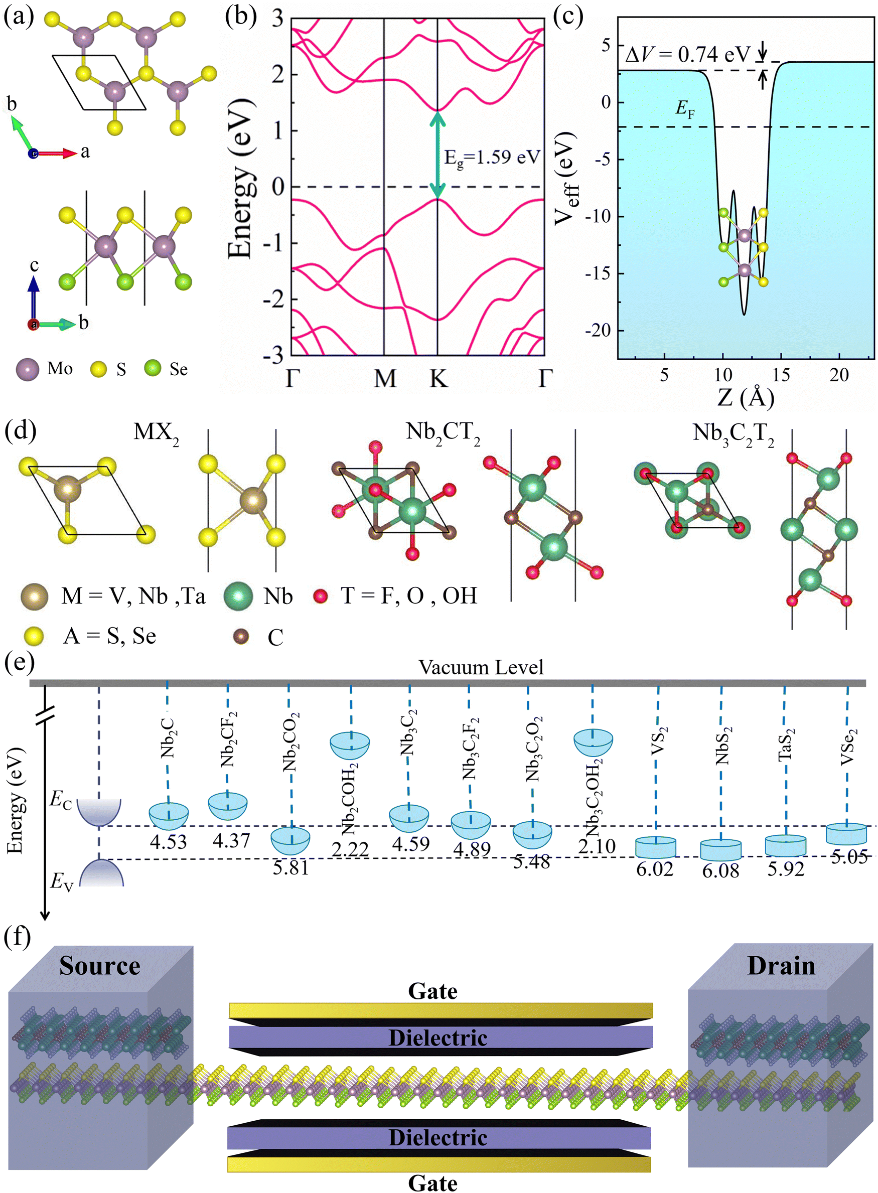 | ||
| Fig. 1 (a) Top and side views of the optimized structure, (b) band structure, and (c) effective electrostatic potential of the MoSSe monolayer. (d) Top and side views of 2D metals. (e) The band alignments between MoSSe and work functions of 2D metals, Ec and Ev represent the energy levels of CBM and VBM for MoSSe monolayer, respectively. (f) Schematic diagram of 2D metal–MoSSe FETs. | ||
Next, we investigated the contact characteristics of MSJs formed between MoSSe monolayer and various 2D metals, including metallic MXenes Nb2C, Nb3C2, Nb2CT2 (T = F, O, OH), Nb3C2T2 (T = F, O, OH), and metallic TMDs MX2 (M = V, Nb, Ta; X = S, Se). Fig. 1d shows the geometrical structures of the studied 2D metals. The band structures of all these 2D metals have many electronic states crossing the Fermi level, which are represented in Fig. S1 (ESI†), indicating their excellent conductivity and potential as metal electrodes. Fig. 1e shows the band edge alignments of MoSSe monolayer and the work functions of the studied 2D metals. To ensure a comprehensive study of metal–MoSSe contacts, we selected 2D metals with a wide range of work function values from 2.10 to 6.08 eV. Herein, the minimum (maximum) work functions of 2D metals are lower (larger) than the EC (EV) of MoSSe monolayer. Meanwhile, the work functions of the 2D metals can be continuously varied within the bandgap of MoSSe monolayer and thus can effectively study the interaction law of the metal–MoSSe contacts. The schematic diagram of MoSSe-based FET model is presented in Fig. 1f, where the 2D metal serves as the source and drain electrodes, and the MoSSe monolayer serves as the channel material of the device.
Among these 2D metals, the optimized lattice constants lie in the range from 3.11 to 3.35 Å, leading to less than 5% lattice mismatch (as listed in Table 1) relative to the MoSSe monolayer (3.25 Å). In the following, 2D metal–MoSSe contacts formed by placing 2D metals on the top of the Se and S sides of the MoSSe monolayer, where 2D metals contact with the Janus MoSSe monolayers on its Se and S sides, are named metal-SeMoS contacts and metal-SMoSe contacts, respectively. In addition, 2D metal–MoSSe contact represents both metal-SeMoS and metal-SMoSe cases. For each type of 2D MSJs, there are six different possible heterostructure stacking configurations, as shown in Fig. S2 (ESI†). We summarized the relative total energies of 2D metal–MoSSe contacts in Tables S1–S3 (ESI†). Furthermore, the 2D MSJs with stacking configuration with the lowest total energy are selected for the subsequent calculations. We defined the metal-semiconductor interlayer distance as the average distance between the Se or S atoms on top of MoSSe and the atoms at the bottom of the 2D metal.36 In most 2D metal–MoSSe contacts, the equilibrium interlayer distance ranges from 2.59 and 3.12 Å, which are typical vdW interactions.37 However, the Nb2C and Nb3C2 systems without and with –OH surface functional groups have smaller interlayer distances, indicating relatively strong interactions. Among them, the Nb2C and Nb3C2 systems with –OH surface functional groups have strong interactions due to hydrogen bonding. The bare Nb2C and Nb3C2 systems have a large number of dangling bonds on the surface, resulting in strong orbital coupling with the MoSSe layer. To further understand the binding strength of the MSJ interface, the binding energy (Eb) was calculated as38
 | (1) |
| 2D metal | ε (%) | W M (eV) | d (Å) | E b (meV Å−2) | Φ SBH (eV) | |||
|---|---|---|---|---|---|---|---|---|
| Se | S | Se | S | Se | S | |||
| Nb2C | 4.17 | 4.53 | 2.62 | 1.68 | −155.17 | −201.38 | — | — |
| Nb2CF2 | 1.56 | 4.37 | 2.82 | 2.59 | −29.07 | −28.41 | 0.77 (n) | 0.18 (n) |
| Nb2CO2 | 3.83 | 5.81 | 2.90 | 2.73 | −35.29 | −32.82 | 0.03 (p) | 0.41 (p) |
| Nb2COH2 | 1.56 | 2.22 | 3.09 | 3.09 | −56.21 | −69.37 | −0.10 (n) | −0.17 (n) |
| Nb3C2 | 2.77 | 4.59 | 2.61 | 1.68 | −161.56 | −212.77 | — | — |
| Nb3C2F2 | 4.50 | 4.89 | 2.85 | 2.64 | −30.27 | −29.64 | 0.50 (p) | 0.33 (n) |
| Nb3C2O2 | 3.18 | 5.48 | 2.82 | 2.83 | −35.79 | −37.29 | 0.05 (p) | 0.58 (p) |
| Nb3C2(OH)2 | 3.80 | 2.10 | 1.99 | 2.08 | −57.55 | −71.35 | −0.33 (n) | −0.28 (n) |
| VS2 | 2.20 | 6.02 | 3.12 | 2.93 | −30.22 | −29.37 | 0.06 (p) | 0.47 (p) |
| NbS2 | 3.08 | 6.08 | 3.01 | 2.86 | −32.39 | −30.13 | 0.08 (p) | 0.46 (p) |
| TaS2 | 2.77 | 5.92 | 3.02 | 2.95 | −31.07 | −29.16 | 0.11 (p) | 0.57 (p) |
| VSe2 | 3.38 | 5.46 | 3.11 | 3.01 | −30.85 | −30.10 | 0.50 (p) | 0.43 (n) |
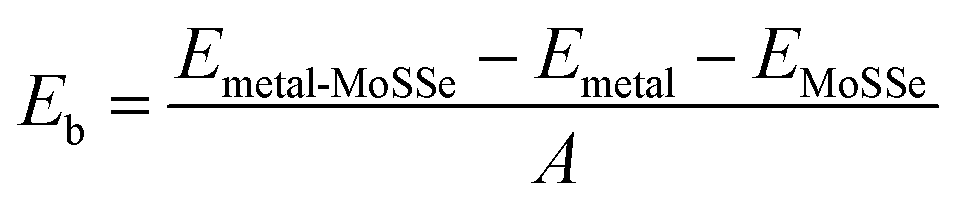
The contact properties of MSJs are mainly dominated by the SBH, which is defined as the energy difference between the Fermi level and the conduction band minimum (CBM) or valence band maximum (VBM) of the semiconductor in the MSJ.39,40
| Φn = EC − EF | (2) |
| Φp = EF − EV | (3) |
 | ||
| Fig. 2 Schematic diagram and the projected band structures of the corresponding metal–MoSSe with (a) Schottky contact, (b) Ohmic contact, (c) quasi-Ohmic contact. The red and gray spheres represent the contributions from MoSSe and metal layers, respectively. | ||
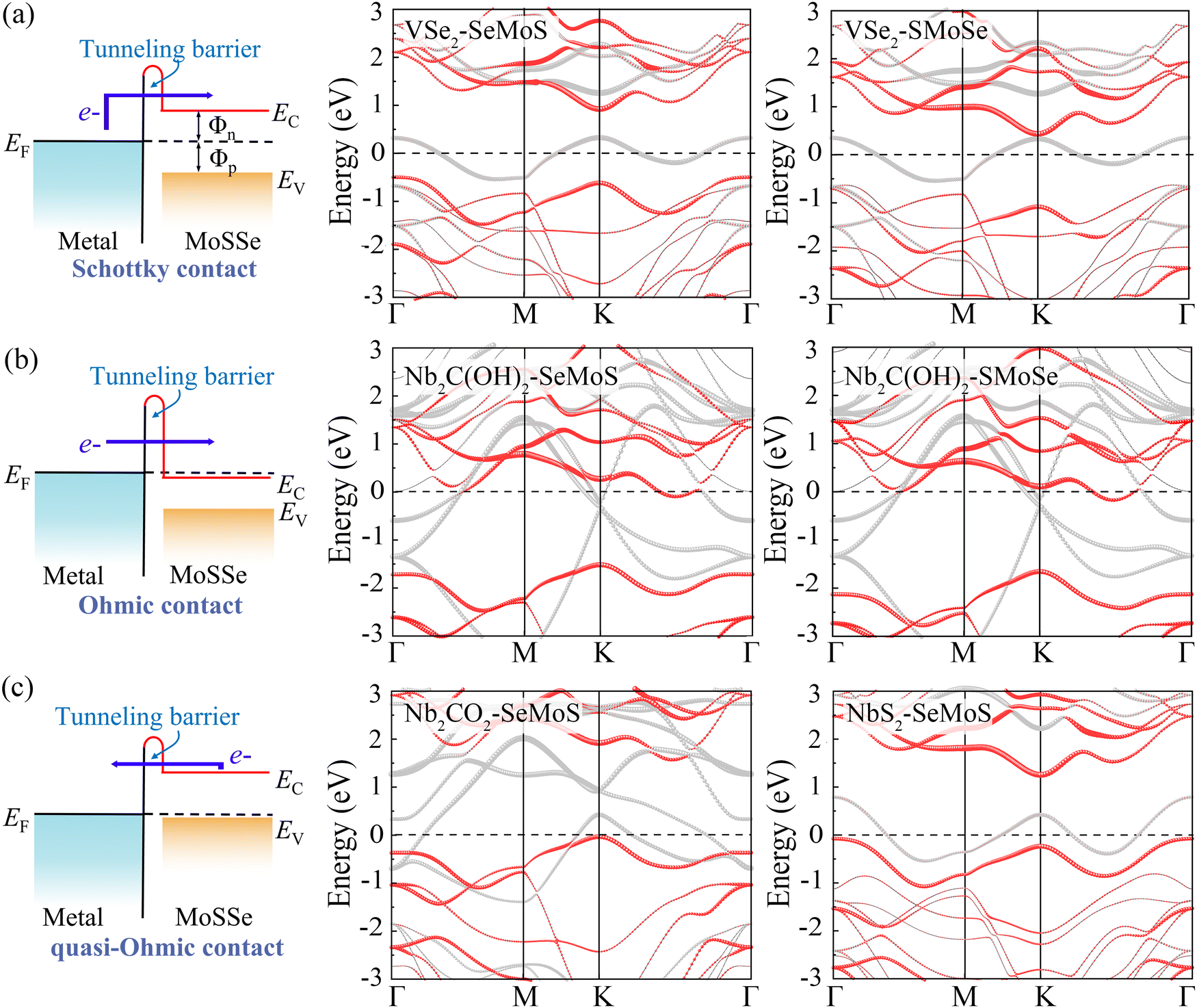
To further analyze the local chemical bonding environments, Fig. 3a depicts the 2D plots of electron localization function (ELF) for typical 2D metal–MoSSe contacts. The ELF is calculated on a 3D grid space using a single determinantal wavefunction derived from the calculated Kohn–Sham orbitals.41,42 The ELF value is a quantitative description of the electron density localization, ranging from 0 to 1, where 1 indicates perfect localization and 0.5 represents gas-like pair probability. The strength of a bond can be characterized by the bond point in the ELF, which corresponds to the saddle point with two negative eigenvalues and one positive eigenvalue.43 Herein, the interfacial bond points of 2D metal–MoSSe contacts can be simply reflected by the minimum value at the center of the ELF line profile curves, as shown in Fig. 3b and Fig. S4 (ESI†).44 Due to the similar characteristics displayed by the contacts of 2D metals with Se and S sides, we analyzed Nb2C-SeMoS and MX2–SeMoS as examples to evaluate the bond strength, as shown in Fig. 3a and b. The Nb2C-SeMoS contact exhibits the largest ELF bond point value of 0.18 for the Nb–Se bond, indicating strong orbital overlap and covalent-like interfacial interactions. In contrast, the values of the ELF bond points of X–Se (X = F, O, S, Se) in the other Nb2CT2–SeMoS contacts are lower, indicating weak atomic orbital overlap and interfacial interactions. Among the Nb2CT2–SeMoS contacts (T = F, O, OH), the H–Se bond point in the Nb2C(OH)2–SeMoS contact exhibits relatively larger value, which also corresponds to their relatively larger binding energy and smaller interlayer distance. The other 2D metal–MoSSe contacts exhibited similar results, as shown in Fig. S4 (ESI†).
 | ||
| Fig. 3 The ELF 2D line profiles and bond points of (a) X–Se bonds in 2D metal-SeMoS contacts and (b) X–S bonds in 2D metal-SMoSe contacts. The pentagrams represent the positions of the bond points. The plane averaged charge density differences for (c) Nb2C-SeMoS and (d) NbS2–SMoSe contacts. | ||
To further understand the electronic properties of MSJs, the plane-averaged charge density difference (Δρ) is calculated as
| Δρ = ρmetal–MoSSe − ρmetal − ρMoSSe | (4) |
The desired 2D MSJs can be achieved by tuning the SBH through the use of metals with different work functions. It is essential to comprehend the FLP effect to analyze the interface properties and the role of interface dipoles. The FLP factor S is calculated as follows.19,47
 | (5) |
![[thin space (1/6-em)]](https://www.rsc.org/images/entities/char_2009.gif) cosφ/εε0. Therefore, we can correct the SBH by ΔV. The larger ΔV indicates that the FLP effect is stronger, resulting in more deviation from the Schottky–Mott limit. Therefore, the modification of SBH by Φn minus ΔV can be achieved. Fig. 4c and d show that the FLP factors S of the metal-SeMoS and metal-SMoSe contacts are 0.45 and 0.31, respectively. Thus, the FLP ability of the Se side of MoSSe monolayer is weaker than that of the S side due to the larger ΔV in the S side observed in Fig. 4b. The corrected FLP factor S of metal-SeMoS and metal-SMoSe contacts can reach 0.99, almost reaching the Schottky–Mott limit. This phenomenon further verifies that the deviation from the Schottky–Mott limit of the FLP effect in 2D MSJs is mainly caused by the interface dipole, where the deviation strength is related to the magnitude of the interfacial dipoles. Therefore, it prospectively hinders the FLP effect by weakening the interlayer coupling between the 2D metal and MoSSe monolayer. As a result, the strength of the interfacial dipoles can be reduced, which leads to an ideal band alignment and a reduced SBH. Furthermore, it is noted that the strength of Dint is related to the electronegativity (which represents the ability of an element to attract electrons) of the terminal atoms on the contact interface.48 Since the electronegativity of the S element (2.58) is greater than that of the Se element (2.55), a larger Dint is exhibited when the S side of MoSSe monolayer is in contact with the 2D metals, resulting in a stronger FLP effect, further deviating from the ideal Schottky–Mott limit.
cosφ/εε0. Therefore, we can correct the SBH by ΔV. The larger ΔV indicates that the FLP effect is stronger, resulting in more deviation from the Schottky–Mott limit. Therefore, the modification of SBH by Φn minus ΔV can be achieved. Fig. 4c and d show that the FLP factors S of the metal-SeMoS and metal-SMoSe contacts are 0.45 and 0.31, respectively. Thus, the FLP ability of the Se side of MoSSe monolayer is weaker than that of the S side due to the larger ΔV in the S side observed in Fig. 4b. The corrected FLP factor S of metal-SeMoS and metal-SMoSe contacts can reach 0.99, almost reaching the Schottky–Mott limit. This phenomenon further verifies that the deviation from the Schottky–Mott limit of the FLP effect in 2D MSJs is mainly caused by the interface dipole, where the deviation strength is related to the magnitude of the interfacial dipoles. Therefore, it prospectively hinders the FLP effect by weakening the interlayer coupling between the 2D metal and MoSSe monolayer. As a result, the strength of the interfacial dipoles can be reduced, which leads to an ideal band alignment and a reduced SBH. Furthermore, it is noted that the strength of Dint is related to the electronegativity (which represents the ability of an element to attract electrons) of the terminal atoms on the contact interface.48 Since the electronegativity of the S element (2.58) is greater than that of the Se element (2.55), a larger Dint is exhibited when the S side of MoSSe monolayer is in contact with the 2D metals, resulting in a stronger FLP effect, further deviating from the ideal Schottky–Mott limit.
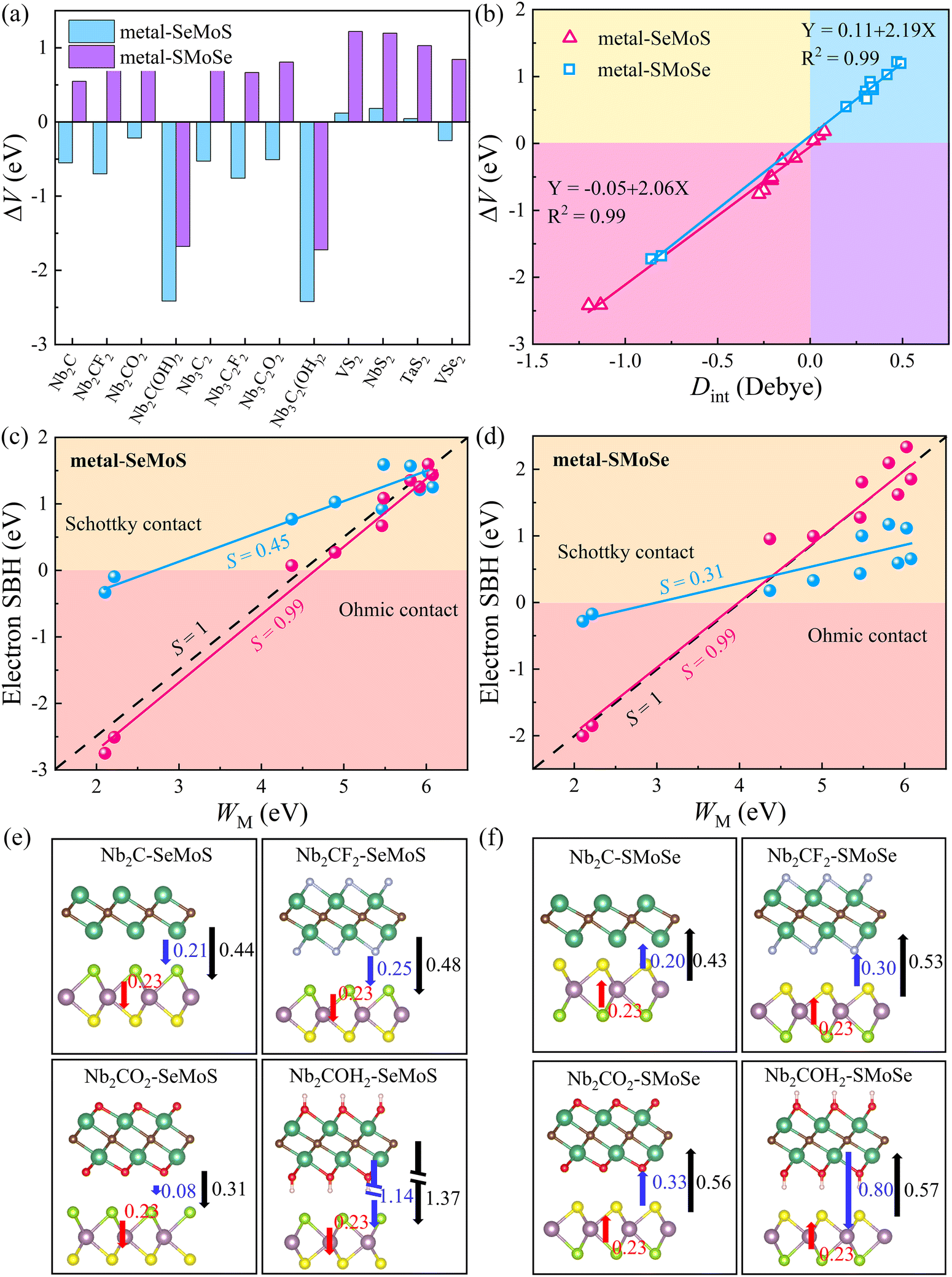 | ||
| Fig. 4 (a) The electronic potential difference (ΔV) in 2D metal–MoSSe contacts. (b) The change in ΔV with interface dipole (Dint) for 2D metal–MoSSe contacts. The variation in the electron SBH as a function of metal work functions (WM) for (c) metal-SeMoS (d) metal-SMoSe contacts. The azure and pink lines represent fitting results without and with ΔV correction, respectively. The black dotted line represents the Schottky–Mott limit S = 1. The Fermi level pinning factor S is defined as the value of the fitted slope. The dipole moment distributions in selected (e) 2D metal-SeMoS and (f) 2D metal-SMoSe contacts. The red, blue, and black arrows represent the intrinsic dipole, interface dipole, and total dipole, respectively. | ||
On the other hand, intrinsic dipoles are also presented in the MoSSe monolayer. Therefore, we further studied the role of the total dipole moment Dtot = D0 + Dint, where D0 is the intrinsic dipole. As shown in Fig. 4e, f and Fig. S6 (ESI†), when the 2D metal contacts MoSSe monolayer with the Se side, the interface dipoles and intrinsic dipoles of VS2, NbS2, and TaS2 are in opposite directions, resulting in a smaller Dtot. For the other metal–MoSSe contacts, the larger Dtot was generated due to the same orientation of the interface dipoles and intrinsic dipoles. In contrast, when the 2D metal contacts MoSSe monolayer with the S side, the interface dipoles and intrinsic dipoles of the low work function metals (Nb2C(OH)2 and Nb3C2(OH)2) are in opposite directions, resulting in a minor Dtot. In comparison, the other metals in contact with the Se sides lead to larger Dtot due to the same orientation of interface dipoles and intrinsic dipoles. The superposition effect of interface and intrinsic dipoles increases the ΔV, resulting in a stronger FLP effect deviating from the Schottky–Mott limit. On the other hand, ΔV is also linearly related to the total dipole moment Dtot for 2D metal–MoSSe contacts, as shown in Fig. S7 (ESI†).
Fig. 5a demonstrates that a p-type Schottky contact is formed more favorably when Nb3C2F2 with lower work function contacts the Se side. The work function of the Se side is greater than that of the Nb3C2F2 side after contact, leading to a negative ΔV in the Nb3C2F2–SeMoS contact. On the other hand, Fig. 5b shows that n-type Schottky contact formation is also favored when Nb3C2F2 contacts the S side; the work function of the S side is lower than that of the Nb3C2F2 side, resulting in a positive ΔV. Furthermore, due to the extremely low work function of Nb2C(OH)2 and (Nb3C2(OH)2), ΔV is consistently negative regardless of the contact with the Se or S side. Conversely, when high work function metals contact the Se or S sides, p-type contact formation is more favorable, and ΔV is always positive. In short, the metal-SeMoS and metal-SMoSe contacts typically generate oppositely-oriented interface dipoles. This phenomenon is also known as the pushback effect or pillow effect, which is caused by the redistribution of electrons by Pauli exchange repulsion.52 The effective electrostatic potential illustrated in Fig. 5a, b and Fig. S8, S9 (ESI†) determines the electrostatic potential difference ΔV and tunneling barrier (TB). Herein, a large TB formed at the MSJs can impede the carrier injection efficiency. We proposed the tunnel barrier height ΦTB and width wTB as two parameters to characterize TB, as listed in Table S4 (ESI†).
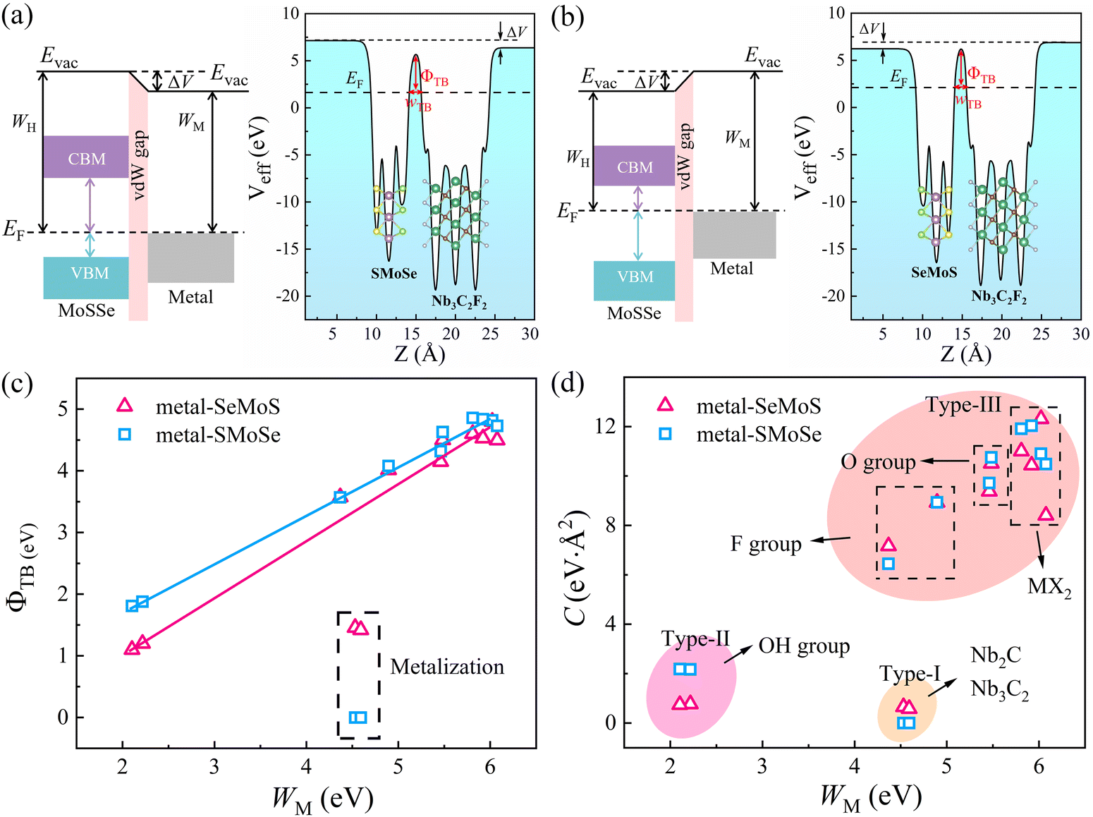 | ||
| Fig. 5 The energy level schematic diagram and effective electrostatic potential of (a) Nb3C2F2–SeMoS and (b) Nb3C2F2–SMoSe contacts. The variation of (c) tunnel barrier height ΦTB and (d) comprehensive factor C as a function of metal work functions for 2D metal–MoSSe contacts. | ||
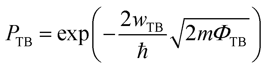
The efficiency of carrier injection can be evaluated by the tunneling probability PTB; the tunneling probability equal or close to 100% can promote the carrier injection efficiency. The tunneling probability PTB is defined as50
 | (6) |
To further investigate the role of interface dipoles in 2D MSJs, we calculated the electronic properties of 2D metal–MoSSe contacts with different MoSSe layer numbers and biaxial strains. As shown in Fig. 6a and b, the results revealed that the band gap of the semiconductor in the Nb3C2F2–SeMoS contact gradually decreases with increasing MoSSe layer numbers. Additionally, the valence band moves closer to the Fermi level, resulting in a quasi-Ohmic contact. In contrast, for the Nb3C2F2–SMoSe contact, the conduction band moves down and crosses the Fermi level, forming an Ohmic contact with increasing MoSSe layer numbers. Furthermore, it can be observed from Fig. 6c and d that as the number of MoSSe layers increases, the Φn and Φp values of the Nb3C2F2–MoSSe contacts also gradually decrease. Simultaneously, the interface dipoles gradually increase and the band gap of the semiconductor layer decreases, indicating that interlayer coupling between Nb3C2F2 and MoSSe is gradually enhanced with increasing MoSSe layer numbers. Tables S5 and S6 (ESI†) list the detailed results for electronic SBH Φn, hole SBH Φp, interface dipole Dint, total dipole Dtot, potential step ΔV, work function difference ΔW, and metal work functions WM for 2D MSJs with different MoSSe layer numbers.
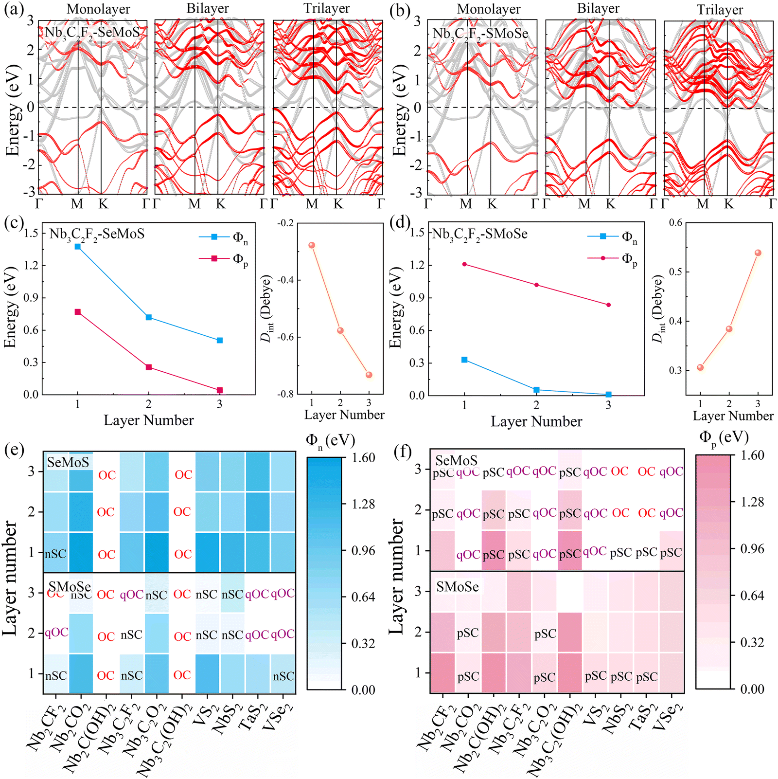 | ||
| Fig. 6 The projected band structures of (a) Nb3C2F2–SeMoS and (b) Nb3C2F2–SMoSe contacts with monolayer, bilayer, and trilayer MoSSe. Schottky barriers and interface dipole of (c) Nb3C2F2–SeMoS and (d) Nb3C2F2–SMoSe contacts as a function of MoSSe layer number. Schottky barrier heights (e) Φn and (f) Φp of 2D metal–MoSSe contacts with different MoSSe layer numbers. OC means Ohmic contact, qOC means quasi-Ohmic contact (Φn or Φp < 0.05 eV), nSC and pSC represent n-type and p-type Schottky contacts, respectively. | ||
Based on the Φn and Φp values obtained from the energy band diagrams, we plot heatmaps of Φn and Φp for 2D MSJs with different numbers of MoSSe layers in Fig. 6e and f, respectively. Negative Φn and Φp values are set to zero since the Ohmic contact is achieved when the SBHs become negative. It is noted that the Φn and Φp values of 2D metal–MoSSe both show a decreasing trend as the number of layers increases. Furthermore, the Φn and Φp values of 2D MSJs are strongly influenced by two important parameters: firstly, the 2D metal–MoSSe contact with Se and S sides leads to different SBHs. Secondly, the use of metals with different work functions leads to different SBHs. Interestingly, as the number of MoSSe layers increases, the Φn values of Nb2C(OH)2 and Nb3C2(OH)2 in contact with MoSSe are always 0, indicating the formation of Ohmic contacts. Additionally, the 2D metal-SeMoS contacts are more inclined to form p-type contacts. As the number of MoSSe layer number increases, significantly low Φp values are obtained to form p-type quasi-Ohmic contacts for Nb2CO2–SeMoS, Nb3CO2–SeMoS, VS2–SeMoS, and VSe2–SeMoS cases. Conversely, n-type Ohmic contacts are preferred for 2D metal-SMoSe contacts. Therefore, the variation in the number of semiconductor layers in MSJs can regulate the values of SBH. To further understand the influence of the strength of the interface dipole on the FLP, we studied the variation in the electronic SBH and the metal work function of 2D metal–MoSSe contacts. By fitting the slope, we obtained the value of the FLP factor S. As shown in Fig. S10 (ESI†), the increase in the number of semiconductor layers leads to a decrease in the FLP factor, indicating an enhanced FLP effect. The decrease in the FLP factor also corresponds to the enhancement of the interface dipole, as shown in Fig. S10c and d (ESI†).
To explore the strain engineering of electronic structure and the SBHs for 2D MSJs, we further investigated the 2D metal–MoSSe contacts under biaxial strains from −6% to 6%. By taking the TaS2–MoSSe contacts as examples, we found that the bandgap of the MoSSe layer changes gradually with increasing tensile or compressive strains, as shown in Fig. 7a and b. Herein, both the valence and conduction bands tend to gradually move closer to the Fermi level with increasing tensile strain for both TaS2–SeMoS and TaS2–SMoSe contacts. It is interesting to note that the valence band moves up through the Fermi level to form an Ohmic contact with 4% tensile strain for the TaS2–SeMoS contact. It is noted that the calculated Φn and Φp values are significantly affected by the variation of strain values, as shown in Fig. 7c and d. The TaS2–SeMoS contact transforms into p-type Ohmic contact at 6% tensile strain, while the TaS2–SMoSe contact transforms from p-type to n-type Schottky contact at compression strains greater than −2%. At the same time, regardless of whether TaS2 contacts the MoSSe monolayer with the Se or S sides, the strain free interface dipole is the smallest, indicating weak interlayer coupling between TaS2 and MoSSe at this point. The results show the possibility of Schottky to Ohmic contact transition under strain. Tables S7 and S8 (ESI†) list the detailed results for electronic SBH Φn, hole SBH Φp, interface dipole Dint, total dipole Dtot, potential step ΔV, work function difference ΔW, and metal work functions WM for 2D MSJs under different strains.
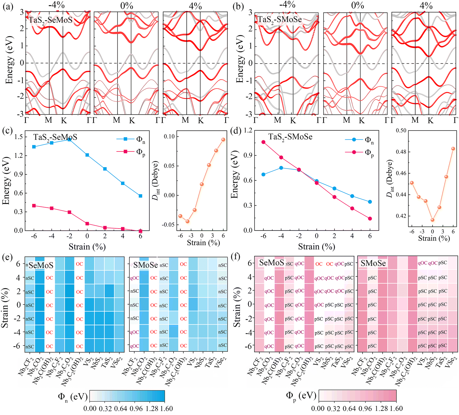 | ||
| Fig. 7 The projected band structures of (a) TaS2–SeMoS and (b) TaS2–SMoSe contacts with different in-plane biaxial strains. Schottky barriers and interface dipole of (c) TaS2–SeMoS and (d) TaS2–SMoSe as a function of biaxial strains. Schottky barrier heights (e) Φn and (f) Φp of 2D metal-SeMoS and metal-SMoSe contacts with different biaxial strains. OC means Ohmic contact, qOC means quasi-Ohmic contact (Φn or Φp < 0.05 eV), nSC and pSC represent n-type and p-type Schottky contacts, respectively. | ||
Fig. 7e and f present the Φn and Φp heatmaps of 2D metal–MoSSe contacts under different biaxial strains, respectively. Interestingly, the contact types of Nb2C(OH)2, Nb3C2(OH)2, Nb2CO2, and Nb3C2O2 contacts remain unchanged within the studied strain range, where the n-type Ohmic contact (–OH terminated) and p-type quasi-Ohmic contact (–O terminated) characteristics are always maintained. As the biaxial strain changes from −6% to 6%, the Φp value of the high work function metals (VS2, NbS2, TaS2) contact gradually decreases and approaches 0, forming a p-type quasi-ohmic contact. The opposite trend is observed for 2D metal-SMoSe contacts, which favors the formation of n-type Ohmic contact. Therefore, we proposed that the SBH can also be tuned by applying biaxial strains. The FLP strength under different biaxial strains is fitted from the relationship between SBH and metal work function in Fig. S11a and b (ESI†). For the metal-SeMoS contacts, the fitted FLP factor S obtained is hardly affected by the compressive strain. Applied −6% compression strain could only slightly increase the FLP factor S to 0.46 (from 0.45 without strain). With the increase in tensile strain, the FLP factor S gradually decreases. The FLP factor S of 0.26 at 6% indicates that the applied tensile strains lead to a stronger FLP effect. On the other hand, the 2D metal-SMoSe contact exhibits a similar phenomenon, the only difference is that the value of the FLP factor S is slightly decreased to 0.29 under −6% compressive strain (from 0.31 without strain). This phenomenon is primarily attributed to the variation of the interface dipole values under strains, as shown in Fig. S11c and d (ESI†). As the tensile strain increases, the interface dipoles are continuously enhanced, leading to a larger ΔV and deviation from the ideal Schottky–Mott limit restrictions. This deviation results in a stronger FLP effect, which is indicated by an increase in the FLP factor S. Conversely, under different compressive strains, the interface dipole values for most 2D metal–MoSSe contacts are relatively close, resulting in a limited change in the FLP factor S.
Despite extensive research into tuning the Schottky barrier, achieving optimal operational efficiency and device performance remains challenging. Therefore, we explored the factors that affect the SBH using modern machine learning models, specifically through the sure-independence-screening-sparsifying-operator (SISSO) method with first-principles calculation results as inputs.33 The SISSO method is a data analysis technique based on compressed sensing, which enables the identification of an optimal low-dimensional feature descriptor from a vast number of features.53 For material data, SISSO can construct a formula that describes a specific property of the material by incorporating several relevant characteristics or descriptors.54 The trained model can predict the desired property of new materials using their values of the descriptors. Tables S5–S8 (ESI†) list the 180 first-principles calculation results for the SISSO machine-learning study. Herein, we used the material property columns of interest, including Φn, Φp, Dint, Dtot, ΔV, ΔW, and WM as descriptors to train the SISSO model. Using selected primary feature classes (PFs), SISSO iteratively generates feature combinations by applying various mathematical operators, such as +, −, ×, /, exp, exp−, −1, 2, 3, and √. Finally, the features generated by SISSO are ranked according to the root mean square error (RMSE) to identify the optimal set of descriptors.55 This approach enables us to gain a deeper understanding of the complex factors that contribute to the SBH, which is critical for developing high-performance MSJs.
Since only the produced descriptors with high precision and low complexity are suitable for regulating SBH, Fig. 8a and b display the Pareto charts for six proposed formulas from SISSO that satisfy the criteria of both simplicity and accuracy. The detailed mathematical form and fitting error of the six formulas are shown in Table 2. It is noted that the increase in complexity cannot guarantee a decrease in the fitting error. Among them, the complexity of 4 is the best compromise between complexity and accuracy for both Φn and Φp. To clearly show the correlation, Fig. 8c and d depict the relationships of SBHs Φn and Φp with 0.01WM3/exp(Dint). The correlations between other mathematical formulas and Φn/Φp are also displayed in Fig. S12 (ESI†) for reference. It is observed that both Φn and Φp exhibit good linear relationships with 0.01WM3/exp(Dint). Thus, we can regulate the SBH by controlling the metal work function WM and metal-semiconductor interface dipole Dint. Specifically, a large WM and small Dint can result in an ideal n-type Ohmic contact and vice versa, and small WM and large Dint can produce a p-type Ohmic contact. Furthermore, adjusting WM and Dint can also achieve quasi-Ohmic contacts with small SBH values. Therefore, by exploring the nonlinear combinations of existing features, the descriptors of WM and Dint are proposed based on the SISSO to fast predict the target properties SBH in MSJs. As shown in Fig. S13 (ESI†), we further examined the SISSO method using supervised training data sampling (sequentially removing the data points with the smallest RMSE) to check the RMSE for different numbers of materials. The results show that the RMSE decreases sharply when the number of data points Nd ranges from 1 to 20. It is worth noting that when Nd falls within the range of 20 to 180, the trend of RMSE decline slows down. These findings suggest that the SISSO model can effectively identify the underlying physical laws even from small datasets in our study.
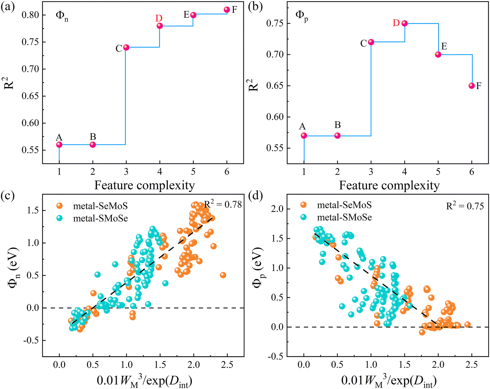 | ||
| Fig. 8 Pareto chart of R2 for (a) Φn and (b) Φpvs. complexity of the proposed mathematical formulas. The correlations of the calculated (c) Φn and (d) Φp values of metal–MoSSe contacts vs. predicted 0.01WM3/exp(Dint) formula from SISSO. The data here are all derived from the DFT calculation results in this work. | ||
| Point | Formulas | Complexity | R2 | |
|---|---|---|---|---|
| Φ n | Φ p | |||
| A | 0.29WM | 1 | 0.56 | 0.57 |
| B | 0.29WM | 2 | 0.56 | 0.57 |
| C | 0.05WM × (WM − ΔV) | 3 | 0.74 | 0.72 |
| D | 0.01WM3/exp(Dint) | 4 | 0.78 | 0.75 |
| E | 0.76(exp(cbrt(WM)) − exp(Dint)) | 5 | 0.80 | 0.70 |
| F | 0.32(abs((log(WM))3 − (exp(Dint))2)) | 6 | 0.81 | 0.65 |
4. Conclusion
In summary, we have systematically investigated the geometric structure, electronic properties, and contacting barrier of MSJs formed by the contact of a series of 2D metals with Janus MoSSe using first-principles calculations. The projected band results indicate that the transition from Schottky contact to Ohmic contact and tunable Schottky barrier can be achieved by selecting different 2D metals. For Nb2C–MoSSe and Nb3C2–MoSSe contacts, strong interactions at the interface lead to the metallization of the bands. In contrast, weak interactions at the interface were observed for Nb2CT, Nb3C2T2 (T = F, O, OH), and MX2 when in contact with the MoSSe monolayer. The FLP effect occurs due to the presence of interface dipoles at the MSJs interface, which deviates the band alignment from the prediction of the ideal Schottky–Mott limit. Furthermore, the values ΔV of 2D metal–MoSSe contacts are linearly related to the interface dipoles. Hence, weakening the interlayer coupling can effectively hinder the FLP effect. Additionally, the tunneling barriers of the 2D metal–MoSSe contacts depend on the interlayer coupling strength, and the ΦTB values also show a good linear relationship with the work functions of 2D metals. Notably, the band edge position of MoSSe is sensitive to both layer numbers and biaxial strains. The results show that increasing the layer number and applying biaxial strain will alter the SBH and lead to the formation of Ohmic contacts. At the same time, the change in the layer number and biaxial strain will also generate different values of interfacial dipoles, affecting the FLP strength. Interestingly, we used the SISSO machine learning algorithm to construct a formula to describe the SBH of the 2D MSJs and tune the SBH. Our research offers valuable insights into tuning the Schottky barriers in MSJs and may facilitate the development of highly efficient Ohmic contacts in future electronic devices.Author contributions
Shu Yu: investigation, formal analysis, writing – original draft. Ting Li: data curation, validation. Naihua Miao: visualization, formal analysis. Jian Gou: visualization, formal analysis. Xiaochun Huang: visualization, writing – review & editing. Rui Xiong: data curation, validation. Zhou Cui: data curation, validation. Cuilian Wen: formal analysis, writing – review & editing. Jian Zhou: formal analysis, writing – review & editing. Baisheng Sa: project administration, supervision, writing –review & editing. Zhimei Sun: supervision, formal analysis, writing – review & editing.Conflicts of interest
The authors declare that they have no conflict of interest.Acknowledgements
This work was supported by the National Key Research and Development Program of China (No. 2022YFB3807200), the National Natural Science Foundation of China (No. 21973012, 21905050, 52222101), the Natural Science Foundation of Fujian Province (No. 2021J06011, 2020J01351, 2020J01474, 2021H6011 and 2021J01590), and the ‘‘Qishan Scholar’’ Scientific Research Project of Fuzhou University.References
- H. Wang, H. Yuan, S. S. Hong, Y. Li and Y. Cui, Chem. Soc. Rev., 2015, 44, 2664–2680 RSC.
- Q. H. Wang, K. Kalantar-Zadeh, A. Kis, J. N. Coleman and M. S. Strano, Nat. Nanotechnol., 2012, 7, 699–712 CrossRef CAS.
- K. F. Mak and J. Shan, Nat. Photonics, 2016, 10, 216–226 CrossRef CAS.
- R. Yang, Y. Fan, Y. Zhang, L. Mei, R. Zhu, J. Qin, J. Hu, Z. Chen, Y. Hau Ng, D. Voiry, S. Li, Q. Lu, Q. Wang, J. C. Yu and Z. Zeng, Angew. Chem., Int. Ed., 2023, 62, e202218016 CrossRef CAS.
- R. P. Li, Y. C. Cheng and W. Huang, Small, 2018, 14, 1802091 CrossRef.
- W. J. Yin, B. Wen, Q. X. Ge, D. F. Zou, Y. Xu, M. W. Liu, X. L. Wei, M. Y. Chen and X. L. Fan, Prog. Natl. Sci.: Mater. Int., 2019, 29, 335–340 CrossRef CAS.
- C. X. Xia, W. Q. Xiong, J. Du, T. X. Wang, Y. T. Peng and J. B. Li, Phys. Rev. B, 2018, 98, 165424 CrossRef CAS.
- A.-Y. Lu, H. Zhu, J. Xiao, C.-P. Chuu, Y. Han, M.-H. Chiu, C.-C. Cheng, C.-W. Yang, K.-H. Wei and Y. Yang, Nat. Nanotechnol., 2017, 12, 744–749 CrossRef CAS.
- Y. Ding, G. F. Yang, Y. Gu, Y. Z. Yu, X. M. Zhang, X. Tang, N. Y. Lu, Y. K. Wang, Z. C. Dai, H. Q. Zhao and Y. H. Li, J. Phys. Chem. C, 2020, 124, 21197–21206 CrossRef CAS.
- H. L. Chen, W. N. Zhang, M. L. Li, G. He and X. F. Guo, Chem. Rev., 2020, 120, 2879–2949 CrossRef CAS.
- B. Jiang, Z. Y. Yang, X. Q. Liu, Y. Liu and L. Liao, Nano Today, 2019, 25, 122–134 CrossRef CAS.
- R. T. Tung, Appl. Phys. Rev., 2014, 1, 011304 Search PubMed.
- J. H. Kang, W. Liu, D. Sarkar, D. Jena and K. Banerjee, Phys. Rev. X, 2014, 4, 031005 CAS.
- J. L. Tao Shen, X. Liu, P. Cheng, J.-C. Ren, S. Li and W. Liu, Adv. Funct. Mater., 2022, 32, 2207018 CrossRef.
- X. C. Liu, M. S. Choi, E. Hwang, W. J. Yoo and J. Sun, Adv. Mater., 2022, 34, 2108425 CrossRef CAS.
- C. Gong, L. Colombo, R. M. Wallace and K. Cho, Nano Lett., 2014, 14, 1714–1720 CrossRef CAS PubMed.
- G. S. Kim, S. H. Kim, J. Park, K. H. Han, J. Kim and H. Y. Yu, ACS Nano, 2018, 12, 6292–6300 CrossRef CAS PubMed.
- P. C. Shen, C. Su, Y. X. Lin, A. S. Chou, C. C. Cheng, J. H. Park, M. H. Chiu, A. Y. Lu, H. L. Tang, M. M. Tavakoli, G. Pitner, X. Ji, Z. Y. Cai, N. N. Mao, J. T. Wang, V. C. Tung, J. Li, J. Bokor, A. Zettl, C. I. Wu, T. Palacios, L. J. Li and J. Kong, Nature, 2021, 593, 211–217 CrossRef CAS PubMed.
- Y. Liu, J. Guo, E. B. Zhu, L. Liao, S. J. Lee, M. N. Ding, I. Shakir, V. Gambin, Y. Huang and X. F. Duan, Nature, 2018, 557, 696–700 CrossRef CAS.
- Y. Y. Liu, P. Stradins and S. H. Wei, Sci. Adv., 2016, 2, e160006 Search PubMed.
- R.-S. Chen, G. Ding, Z. Feng, S.-R. Zhang, W.-A. Mo, S.-T. Han and Y. Zhou, Adv. Funct. Mater., 2022, 32, 2204288 CrossRef CAS.
- V. Kamysbayev, A. S. Filatov, H. C. Hu, X. Rui, F. Lagunas, D. Wang, R. F. Klie and D. V. Talapin, Science, 2020, 369, 979–983 CrossRef CAS PubMed.
- A. Iqbal, F. Shahzad, K. Hantanasirisakul, M. K. Kim, J. Kwon, J. Hong, H. Kim, D. Kim, Y. Gogotsi and C. M. Koo, Science, 2020, 369, 446–450 CrossRef CAS.
- A. VahidMohammadi, J. Rosen and Y. Gogotsi, Science, 2021, 372, eabf1581 CrossRef CAS PubMed.
- M. Li, X. Li, G. Qin, K. Luo, J. Lu, Y. Li, G. Liang, Z. Huang, J. Zhou, L. Hultman, P. Eklund, P. O. Å. Persson, S. Du, Z. Chai, C. Zhi and Q. Huang, ACS Nano, 2021, 15, 1077–1085 CrossRef CAS.
- J. Hafner, J. Comput. Chem., 2008, 29, 2044–2078 CrossRef CAS PubMed.
- J. P. Perdew and Y. Wang, Phys. Rev. B: Condens. Matter Mater. Phys., 1992, 45, 13244–13249 CrossRef PubMed.
- G. J. Wang, L. Y. Peng, K. Q. Li, L. G. Zhu, J. Zhou, N. H. Miao and Z. M. Sun, Comput. Mater. Sci., 2021, 186, 110064 CrossRef CAS.
- K. Parlinski, Z. Q. Li and Y. Kawazoe, Phys. Rev. Lett., 1997, 78, 4063–4066 CrossRef CAS.
- J. P. Perdew, K. Burke and Y. Wang, Phys. Rev. B: Condens. Matter Mater. Phys., 1996, 54, 16533 CrossRef CAS PubMed.
- S. Grimme, J. Antony, S. Ehrlich and H. Krieg, J. Chem. Phys., 2010, 132, 154104 CrossRef.
- S. Grimme, S. Ehrlich and L. Goerigk, J. Comput. Chem., 2011, 32, 1456–1465 CrossRef CAS PubMed.
- R. Ouyang, S. Curtarolo, E. Ahmetcik, M. Scheffler and L. M. Ghiringhelli, Phys. Rev. Mater., 2018, 2, 083802 CrossRef CAS.
- S. D. Tao, B. Xu, J. Shi, S. Y. Zhong, X. L. Leio, G. Liu and M. S. Wu, J. Phys. Chem. C, 2019, 123, 9059–9065 CrossRef CAS.
- F. P. Li, W. Wei, P. Zhao, B. B. Huang and Y. Dai, J. Phys. Chem. Lett., 2017, 8, 5959–5965 CrossRef CAS PubMed.
- Y. Shu, Y. Liu, Z. Cui, R. Xiong, Y. Zhang, C. Xu, J. Zheng, C. Wen, B. Wu and B. Sa, Adv. Electron. Mater., 2023, 9, 2201056 CrossRef CAS.
- J. H. Chen, X. J. He, B. S. Sa, J. Zhou, C. Xu, C. L. Wen and Z. M. Sun, Nanoscale, 2019, 11, 6431–6444 RSC.
- X. H. Yang, B. S. Sa, P. Lin, C. Xu, Q. Zhu, H. B. Zhan and Z. M. Sun, J. Phys. Chem. C, 2020, 124, 23699–23706 CrossRef CAS.
- J. Wang, X. Y. Zhou, M. J. Yang, D. Cao, X. S. Chen and H. B. Shu, J. Mater. Chem. C, 2020, 8, 7350–7357 RSC.
- Q. Peng, C. Si, J. Zhou and Z. M. Sun, Appl. Surf. Sci., 2019, 480, 199–204 CrossRef CAS.
- B. Silvi and A. Savin, Nature, 1994, 371, 683–686 CrossRef CAS.
- A. D. Becke and K. E. Edgecombe, J. Chem. Phys., 1990, 92, 5397–5403 CrossRef CAS.
- B. Sa, J. Zhou, Z. Sun, J. Tominaga and R. Ahuja, Phys. Rev. Lett., 2012, 109, 096802 CrossRef.
- B. Sa, N. Miao, Z. Sun and B. Wu, RSC Adv., 2015, 5, 1690–1696 RSC.
- R. Xiong, R. Hu, Y. G. Zhang, X. H. Yang, P. Lin, C. L. Wen, B. Sa and Z. M. Sun, Phys. Chem. Chem. Phys., 2021, 23, 20163–20173 RSC.
- X. Zhang, L. Feng, S. Zhong, Y. Ye, H. Pan, P. Liu, X. Zheng, H. Li, M. Qu and X. Wang, Sci. China: Mater., 2023, 66, 811–818 CAS.
- Q. Q. Wang, L. M. Cao, S. J. Liang, W. K. Wu, G. Z. Wang, C. H. Lee, W. L. Ong, H. Y. Yang, L. K. Ang, S. Y. A. Yang and Y. S. Ang, npj 2D Mater. Appl., 2021, 5, 71 CrossRef CAS.
- J. Li, W. Q. Liu, W. H. Zhou, J. L. Yang, H. Z. Qu, Y. Hu and S. L. Zhang, Phys. Rev. Appl., 2022, 17, 054009 CrossRef.
- J. Li, W. H. Zhou, L. L. Xu, J. L. Yang, H. Z. Qu, T. T. Guo, B. Xu, S. L. Zhang and H. B. Zeng, Mater. Today Phys., 2022, 26, 100749 CrossRef CAS.
- T. Shen, J. C. Ren, X. Y. Liu, S. Li and W. Liu, J. Am. Chem. Soc., 2019, 141, 3110–3115 CrossRef CAS PubMed.
- M. Bruening, R. Cohen, J. F. Guillemoles, T. Moav, J. Libman, A. Shanzer and D. Cahen, J. Am. Chem. Soc., 1997, 119, 5720–5728 CrossRef CAS.
- M. Farmanbar and G. Brocks, Phys. Rev. B, 2016, 93, 085304 CrossRef.
- G. Cao, R. Ouyang, L. M. Ghiringhelli, M. Scheffler, H. Liu, C. Carbogno and Z. Zhang, Phys. Rev. Mater., 2020, 4, 034204 CrossRef CAS.
- B. Weng, Z. Song, R. Zhu, Q. Yan, Q. Sun, C. G. Grice, Y. Yan and W.-J. Yin, Nat. Commun., 2020, 11, 3513 CrossRef CAS PubMed.
- S. H. V. Oh, W. Hwang, K. Kim, J. H. Lee and A. Soon, Adv. Sci., 2022, 9, 2104569 CrossRef CAS PubMed.
Footnote |
| † Electronic supplementary information (ESI) available. See DOI: https://doi.org/10.1039/d3nh00450c |
| This journal is © The Royal Society of Chemistry 2024 |