
Multistate switching of scanning tunnelling microscopy machined polyoxovanadate–dysprosium–phthalocyanine nanopatterns on graphite†
Marco
Moors
 ,
Irina
Werner
,
Jens
Bauer
,
Jonas
Lorenz
and
Kirill Yu.
Monakhov
*
,
Irina
Werner
,
Jens
Bauer
,
Jonas
Lorenz
and
Kirill Yu.
Monakhov
*
Leibniz Institute of Surface Engineering (IOM), Permoserstraße 15, Leipzig 04318, Germany. E-mail: kirill.monakhov@iom-leipzig.de
First published on 12th December 2023
Abstract
We demonstrate the first formation of stable, multistate switchable monolayers of polyoxometalates (POMs), which can be electronically triggered to higher charged states with increased conductance in the current–voltage profile at room temperature. These responsive two-dimensional monolayers are based on a fully oxidised dodecavanadate cage (POV12) equipped with Dy(III)-doped phthalocyanine (Pc) macrocycles adopting the face-on orientation on highly oriented pyrolytic graphite (HOPG). The layers can be lithographically processed by the tip of a scanning tunnelling microscope (STM) to machine patterns with diameters ranging from 30 to 150 nm2.
New conceptsThis work demonstrates a fundamentally important departure from STM measurements of single polyoxovanadate molecules to micro-spectroscopic experiments with their 2D layers. The use of STM tip nanomachining has made it possible to create various hole and interconnect structures with adjustable feature sizes in the formed monolayers on graphite. The layers exhibit a redox-controlled multistate switching with staircase conductance transitions. The XPS measurements indicate an intralayer electron communication between polyoxovanadate building blocks, which is likely driven by their counter cations. The obtained results open up exciting opportunities for the future simulation and ultimate implementation of such POM-based hybrid organic–inorganic compounds as potential molecular memristors in energy-efficient in-memory computing technologies. |
The growing demand for smaller and more powerful computing devices has led in recent years to tremendous developments in Complementary Metal Oxide Semiconductor (CMOS) technology. However, the emerging opportunities in computer technology have also enabled to create artificial intelligence (AI) algorithms that consume a large amount of energy. It is expected that devices based on nanomaterials with memory resistive (memristive) properties will improve the energy budget of future information and communication devices.1
In addition to circuit design based on the electrical engineering of technical solid-state material systems to overcome the physical limitations of classical silicon-based micro- and nanoelectronics, approaches to fabricating circuits from molecular switches with dimensions of only a few nanometers have also been extensively explored.2–4 The key advantage of using such low-dimensional compounds with discrete energy levels for circuit design is in reducing contact resistance to achieve faster operation cycles and/or lower power consumption compared to traditional semiconductor materials.5 On the other hand, the ability of chemically designed zero-dimensional single molecules to self-assemble can help reduce some of the costly and energy-consuming steps of lithography in industrial production. Their successful integration (along with other types of nanomaterials such as nanowires,6 nanofilms,7 nanofibers,8 and nanoparticles9) as active switching layers into high-capacity electronic memory devices is of great economic and environmental importance.
Highly stoichiometric molecular metal oxides such as polyoxometalates (POMs) have emerged as a promising chemical class for use in charge-based10–12 and resistive memories.13–15 The development of POMs16,17 as potential molecular memristors, i.e. extremely small data memory elements that can change their logic state information by the potential-induced change in their resistive properties,18,19 should have a positive impact on conventional computing as well as neuromorphic applications.20,21 However, the immobilisation of POMs on various surfaces22 and the revolutionary implementation of POM electronics in technical devices requires solving urgent problems of POM charge stabilisation on surfaces, multistate capacitance switching at room temperature (r.t.), spatially controlled positioning and nano-structuring of POMs, their crosstalk and electrical contacting, and, finally, efficient integration into existing production lines.
Herein, we demonstrate the fundamentally significant transition to the multistate switching of vanadium-containing POM-based layers at room temperature and low potentials. We also succeeded in a remarkable non-destructive modification of these layers into circuit-like nanopatterns by using a scanning tunneling microscopy (STM) based nanolithography approach. An industrially applied version of the latter may be of value in minimising the many different resource- and energy-intensive steps involved in the scalable fabrication of memory cells with multi-level switching POM layers on CMOS compatible surfaces.
Our previous studies have shown successful immobilisation and multistate resistive switching of vanadium-containing POMs as intact single molecules on metal surfaces,23–25 but their stabilisation in the form of stable layer systems has remained a challenge up to now, especially on non-metallic materials like oxides26 or graphite.27 As bulk framework of technologically extremely interesting graphene layers, this is a rather important issue. Graphene-based materials are highly relevant, e.g., to develop advanced supercapacitors,28 photocatalysts,29 or solar cells,30 and they are the basis for new spin logic and memory devices.31 For technological significance, laminar self-assembly of molecular layers on such weakly binding surface systems is necessary due to the extreme difficulty of contacting single molecules.
However, it has been shown that self-assembly of POM layers on graphite surfaces can be complicated by the anionic nature of the POM, which leads to strong intermolecular interactions and promotes three-dimensional (3D) agglomeration instead of closed and ordered two-dimensional (2D) layer structures.27 The most promising approach to solving this problem is the functionalisation of the POM switching-active core with aromatic macrocycles like phthalocyanine (H2Pc). Such a covalent POM ligation will increase the strength of the POM bonding with the graphite surface due to numerous π–π interactions, while simultaneously providing POM charge stabilisation.32
Therefore, we prepared a sub-1 nm molecular layer system based on recently synthesised, DyPc-augmented dodecavanadate cage compounds.33,34 The POMs were immobilised, patterned, and switched by STM on a highly oriented pyrolytic graphite (HOPG) surface. The tubular [HV12O12Cl]4− POM (hereafter referred to as POV12), ligated covalently by DyPc moieties (Fig. 1), exhibits redox-controlled conductance changes at r.t. and at slightly higher operating voltages than the Lindqvist-type POM with a diamagnetic {V6O19} core (POV6). The latter is capable of storing 2 bits of information for its 4 electrically generated logic states on gold.31 The different switching potential of the V(3d) centres in these compounds is due to a significantly larger electronic bandgap of PcDy-POV12 (2.4–2.6 eV) than that of POV6 (1.0–1.2 eV),24,35 which makes them useful components for the development of more complex molecular logic devices. The additional magnetic properties of PcDy-POV12 may also be exploited in that context.36
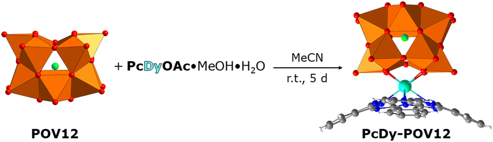 | ||
| Fig. 1 Synthesis of the POM compound (nBu4N)3[HV12O32Cl(DyPc)] (PcDy-POV12) for the fabrication of STM-processed monolayers on HOPG. (nBu4N)4[HV12O32Cl] (POV12) and PcDyOAc·MeOH·H2O were used as starting compounds. Colour code: VO5 polyhedra = orange, O = red, Cl = green, C = dark grey, N = blue, H = white, Dy = aqua. Counter cations and H atoms at the POV12 cage are not shown. | ||
The formation of self-assembled monolayers (SAMs) of PcDy-POV12, depicted in Fig. 2a–c, was performed by immersing of freshly stripped HOPG crystals into a highly diluted (10−6–10−5 mol L−1) acetonitrile (HPLC grade) solution for 2 h. The intact immobilisation of the compound and the formation of 2D layers were confirmed by X-ray photoelectron spectroscopy (XPS) and STM measurements, respectively. Remarkably, the XPS data indicate a rather large amount of 50% partially reduced V(IV) atoms in the 2D layer (Fig. S1, ESI†), which is not observed in pure powder measurements (Fig. S2, ESI†). This high amount of reduced vanadium species can hardly be explained by a simple charge transfer from the non-metallic substrate, which will not allow covalent bonding, but is probably due to a counter cation-mediated charge transfer between POMs within the monolayer. Such a phenomenon has already been reported and theoretically supported for the crystalline phase and highly concentrated solutions of the PcDy-POV12 compound.34 Suggested was hereby a counter cation mediated electron hopping from a Pc moiety of one PcDy-POV12 anion to the POV12 moiety of another PcDy-POV12 anion. Indeed, to specifically determine the POV12 redox states and the physical mechanisms that occur in the PcDy-POV12 layer, it is necessary to carry out additional, time-consuming theoretical studies, which will be published elsewhere. It is noteworthy that such complex electronic interactions of POM anions with their counter cations and the resulting effects on the redox-controlled electron transport characteristics of the POM get more and more attention37 of the experimental38,39 and theoretical40,41 POM communities.
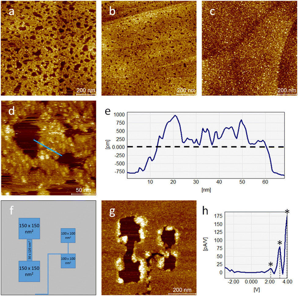 | ||
| Fig. 2 STM images (UB = 2 V; IT = 10 pA) of PcDy-POV12 layers deposited on HOPG by dip-coating the sample into differently concentrated acetonitrile solutions: 1 × 10⁻⁶ mol L−1 (a), 5 × 10⁻⁶ mol L−1 (b), and 1 × 10⁻⁵ mol L−1 (c). (d): high resolution image of (a) and corresponding height profile (e). The baseline at 0 nm represents the top of the molecular monolayer. (f) and (g) show nano-structuring in form of a POV12 circuity formed by the STM tip; (h): dI/dV curve measured on single point in (c) displays three conduction steps due to single electron transfers. The elevated edges of the generated nanostructures in (g) are due to excavated material from the writing process. | ||
STM measurements show that at the lowest investigated concentration the SAMs still exhibit many holes in the film (Fig. 2a), which decrease in size and number with increasing concentration (Fig. 2b) until the film becomes completely closed (Fig. 2c). The film thickness of about 0.75 nm points out the formation of a monolayer (Fig. 2d and e). Although, the presence of additional particles of the same height on top of this main layer indicates the beginning of the growth of the second layer even before the closure of the first. Larger agglomerations are not found over the entire surface. Thus, it can be concluded that strong π–π interactions of the Pc ligands with the graphite surface successfully dominate over intermolecular interactions. Another indicator of this is the rather high stability of STM measurements at larger tip-sample distances. Only at the edges of the holes in the film under these conditions a slight displacement of the material caused by the tip was detected. Subsequent scanning electron microscopy (SEM) measurements (Fig. S4, ESI†) confirmed the long-range morphology of the film growth and, thus, excluded a purely electronic origin of the structures observed by STM.
The measured lateral diameter of the individual particles in the layer is approx. 7 nm (Fig. S3, ESI†), but the extended size of the electronic cloud of a negatively charged complex immobilised on a conducting substrate is a known phenomenon.23,35,42 This confirms the hypothesis that POV12 is an inorganic axial ligand for the DyPc moiety oriented to the HOPG surface. Surface scanning under moderate conditions (UB = +2 V; IT = 10 pA) shows a rather stable adsorption behaviour of the molecular layer, but even a slight decrease of the tip-to-sample-distance by lowering the bias voltage to +1 V results in a reproducible surface removal of the particles already by the first scan. Technically, this can be used to control the structuring of coated surfaces at the nanoscale. As illustrated in Fig. 2f and g, the formation of complex hole structures and interconnections can be realised using the STM tip. Larger structures such as several 100 nm2 sized pads can also be formed as interconnects only a few nm wide. It can be stated that the resulting π–π bonds between the molecules and the surface are strong enough to ensure the ordered formation of a molecular monolayer, but also weak enough to ensure easy modification of the layer by soft electrical or mechanical treatment.
It is known from our previous studies of POV6 as single molecules on gold surfaces that the oxidation states of vanadium centres can be easily modified by an external potential.35I–U measurements of the PcDy-POV12 layer show instead three conductance steps at approx. 2.1, 3.2, and 4.0 V (Fig. 2h). Compared to POV6 (0.6, 1.1, 1.5 and 1.9 V),35 these steps occur at higher potentials, which can be explained by the much larger bandgap of PcDy-POV12. The bandgap difference of approx. 1.5 V corresponds perfectly to the potential difference between the first molecular conductance steps of both species, which are affected by their LUMO. Although this has not yet been clarified by theoretical calculations, each conductance step likely represents a single electron transfer from the STM tip into the unoccupied states of a molecular vanadium centre. Further reduction steps at higher potentials than 4 V may be feasible but cannot be experimentally investigated due to the strong molecular interaction with the STM tip at very high bias voltages. Hereby, the surface layer gets reproducibly damaged, probably due to increased Joule heating, resulting in craters at the corresponding tip position.
Importantly, for the first time, it was possible to demonstrate the multistate switching behaviour within an extended 2D polyoxovanadate layer, rather than just of an isolated immobilised molecule, which is an important step towards technically relevant devices.
To obtain a better understanding of the adsorption and switching characteristics of PcDy-POV12, comparative studies of the bis-ligated derivative (PcDy)2-POV12 and the starting complex PcDyOAc were performed. As can be seen in Fig. 3 both compounds also form closed films without significant defects after the deposition of a 10−5 mol L−1 concentrated acetonitrile solution on HOPG. Like the mono-ligated derivative, (PcDy)2-POV12 exhibits polyoxovanadate-specific switching behaviour (Fig. 3c). While the first observed redox step at a potential of 2.1 V is identical to the monoligated POV12, the second and third steps show slight variations of 2.9 and 3.4 V (compared to 3.2 and 4.0 V, respectively). This indicates that the caping of the PcDy-POV12 cage by an additional macrocyclic DyPc ligand likely does not affect the energy of the lowest unoccupied molecular orbital (LUMO) but lowers the energies of the higher lying unoccupied molecular orbitals. Probably due to intramolecular mixing of the electronic states of the Pc ligands sandwiching the POV12 cage, single particles of the layer appear like unstructured “blobs” in the STM images. However, one can assume a configuration with Pc at the interface between POV12 and the surface and the resulting Pc termination due to extensive π–π interactions. This assumption is supported by the significantly reduced (electronic) particle size of only approx. 5 nm (Fig. S3, ESI†) compared to the monoligated derivative, pointing to a greater distance between the STM tip and the electron rich POV12 cage. These results are in line with the adsorption characteristics of PcDyOAc without POV12 on HOPG. Individual particles in the formed molecular layer exhibit a rather similar size in STM measurements. This confirms that the imaging of (PcDy)2-POV12 is strongly influenced by the electronic structure of the (terminating) Pc ligand. For PcDyOAc without POV12, also sub-molecular resolution could be achieved, showing the characteristic four-lobe structure of Pc43 with an electronic elevation in the centre caused by the Dy atom (Fig. 3f). As expected, the PcDyOAc complex does not exhibit any of the redox-controlled switching characteristics of POV6 and POV12 polyoxovanadates.
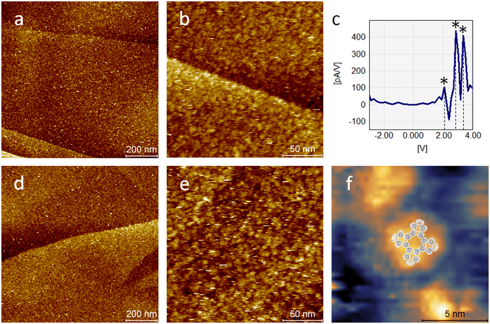 | ||
| Fig. 3 STM images (UB = 2 V; IT = 10 pA) of a (PcDy)2-POV12 layer (a) and (b) with corresponding dI/dV curve (c) measured on a single point in (b) and of a PcDyOAc layer (d) and (e). High resolution imaging of a single PcDyOAc molecule (f) exhibits Pc characteristic fourfold symmetry indicated by the overlay of a calculated metal Pc LUMO structure.43 | ||
In conclusion, this work demonstrates the controlled deposition, nano-structuring, and multielectron charging of V(3d)-based POM layers containing magnetic DyPc functionalities on the non-metallic HOPG surface. The fundamental multistate switching characteristics of single polyoxovanadate anions at r.t. are preserved in their molecular layers. Functionalisation with phthalocyanine ligands ensures sufficiently strong immobilisation of the studied compounds through magnetically doped macrocycles in the form of closed thin films on graphite due to π–π interactions. By adjusting the STM parameters, a reproducible local removal of molecules at the nanoscale was afforded. Compared to the previously studied low-potential POV6 switches (<2 V), POV12 anions can be viewed as their high-potential-switching counterpart (>2 V). Our results lay an important groundwork for the future development of the electronic interplay between both types of molecular switches (POV6 and POV12). In the next step, we will transfer these fundamental observations at the nanoscale to the macroscopic I–V behaviour of technical POM layers. We expect that this might be the key to the realisation of Boolean logic prototype devices and be the next groundbreaking step towards a molecular processor based on integrated POM circuits on CMOS-compatible material systems.
Author contributions
M. M.: STM/STS investigation, data curation, validation, writing and editing – original draft; I. W.: synthesis and characterisation; J. B.: XPS investigation; J. L.: SEM investigation; K. Y. M.: project supervision, conceptualisation, editing – original draft.Conflicts of interest
There are no conflicts to declare.Acknowledgements
The authors acknowledge the support from the Leibniz Association through the Leibniz Collaborative Excellence funding program (project iMolKit) and from the Deutsche Forschungsgemeinschaft (project number 432224404).References
- M.-K. Song, J.-H. Kang, X. Zhang, W. Ji, A. Ascoli, I. Messaris, A. S. Demirkol, B. Dong, S. Aggarwal, W. Wan, S.-M. Hong, S. G. Cardwell, I. Boybat, J. Seo, J.-S. Lee, M. Lanza, H. Yeon, M. Onen, J. Li, B. Yildiz, J. A. del Alamo, S. Kim, S. Choi, G. Milano, C. Ricciardi, L. Alff, Y. Chai, Z. Wang, H. Bhaskaran, M. C. Hersam, D. Strukov, H.-S. P. Wong, I. Valov, B. Gao, H. Wu, R. Tetzlaff, A. Sebastian, W. Lu, L. Chua, J. J. Yang and J. Kim, ACS Nano, 2023, 17, 11994 CrossRef CAS PubMed.
- J. L. Zhang, J. Q. Zhong, J. D. Lin, W. P. Hu, K. Wu, G. Q. Xu, A. T. S. Wee and W. Chen, Chem. Soc. Rev., 2015, 44, 2998 RSC.
- S. Gao, X. Yi, J. Shang, G. Liu and R.-W. Li, Chem. Soc. Rev., 2019, 48, 1531 RSC.
- Y. Li, Q. Qian, X. Zhu, Y. Li, M. Zhang, J. Li, C. Ma, H. Li, J. Lu and Q. Zhang, InfoMat, 2020, 2, 995 CrossRef CAS.
- L. Zhang, K. Xu and F. Wei, J. Mater. Sci., 2023, 58, 2087 CrossRef CAS.
- V. Fra, M. Beccaria, G. Milano, S. Guastella, S. Bianco, S. Porro, M. Laurenti, S. Stassi and C. Ricciardi, Nanotechnology, 2020, 31, 374001 CrossRef CAS PubMed.
- Y. H. Wang, Z. Q. He, X. B. Lai, B. Y. Liu, Y. B. Chen, L. W. Zhang and F. P. Wang, J. Alloys Compd., 2021, 873, 159809 CrossRef CAS.
- J. R. D. Retamal, C. H. Ho, K. T. Tsai, J. J. Ke and J. H. He, IEEE Trans. Electron Devices, 2019, 66, 938 CAS.
- C. Zhang, P.-L. Yu, Y. Li and J.-C. Li, Org. Electron., 2020, 77, 105528 CrossRef CAS.
- O. Badami, T. Sadi, F. Adamu-Lema, P. Lapham, D. Mu, D. Nagy, V. Georgiev, J. Ding and A. Asenov, IEEE Trans. Nanotechnol., 2020, 19, 704 CAS.
- C. Busche, L. Vilá-Nadal, J. Yan, H. N. Miras, D.-L. Long, V. P. Georgiev, A. Asenov, R. H. Pedersen, N. Gadegaard, M. M. Mirza, D. J. Paul, J. M. Poblet and L. Cronin, Nature, 2014, 515, 545 CrossRef CAS PubMed.
- L. Vilá-Nadal, S. G. Mitchell, S. Markov, C. Busche, V. P. Georgiev, A. Asenov and L. Cronin, Chem. – Eur. J., 2013, 19, 16502 CrossRef PubMed.
- X. Chen, Y. Zhou, V. A. L. Roy and S. T. Han, Adv. Mater., 2018, 30, 1703950 CrossRef.
- K. Y. Monakhov, M. Moors and P. Kögerler, Perspectives for Polyoxometalates in Single-Molecule Electronics and Spintronics, in Advances in Inorganic Chemistry, ed. R. van Eldik and L. Cronin, Academic Press, Amsterdam, 2017, p. 251 Search PubMed.
- C. Huez, D. Guérin, S. Lenfant, F. Volatron, M. Calame, M. L. Perrin, A. Proust and D. Vuillaume, Nanoscale, 2022, 14, 13790 RSC.
- M. T. Pope and U. Kortz, Polyoxometalates, in Encyclopedia of Inorganic and Bioinorganic Chemistry, John Wiley & Sons, Ltd., 2012, pp. 1–14 Search PubMed.
- M. Stuckart and K. Y. Monakhov, Vanadium: Polyoxometalate Chemistry, in Encyclopedia of Inorganic and Bioinorganic Chemistry, John Wiley & Sons, Ltd., 2018, pp. 1–19 Search PubMed.
- R. Waser and M. Aono, Nat. Mater., 2007, 6, 833 CrossRef CAS PubMed.
- M. J. Marinella and A. A. Talin, Nature, 2021, 597, 36 CrossRef CAS PubMed.
- G. Zhang, J. Qin, Y. Zhang, G. Gong, Z.-Y. Xiong, X. Ma, Z. Lv, Y. Zhou and S.-T. Han, Adv. Funct. Mater., 2023, 33, 2302929 CrossRef CAS.
- Z. Wang, H. Wu, G. W. Burr, C. S. Hwang, K. L. Wang, Q. Xia and J. J. Yang, Nat. Rev. Mater., 2020, 5, 179 Search PubMed.
- A. S. Cherevan, S. P. Nandan, I. Roger, R. Liu, C. Streb and D. Eder, Adv. Sci., 2020, 7, 1903511 CrossRef CAS PubMed.
- M. Glöβ, R. Pütt, M. Moors, E. Kentzinger, S. Karthäuser and K. Y. Monakhov, Adv. Mater. Interfaces, 2022, 9, 2200461 CrossRef.
- F. Yang, M. Moors, D. A. Hoang, S. Schmitz, M. Rohdenburg, H. Knorke, A. Charvat, X.-B. Wang, K. Y. Monakhov and J. Warneke, ACS Appl. Nano Mater., 2022, 5, 14216 CrossRef CAS.
- K. Y. Monakhov, M. Moors, E. Vogelsberg, J. Lorenz, J. Warneke and F. Yang, IEEE International Interconnect Technology Conference (IITC) and IEEE Materials for Advanced Metallization Conference (MAM)(IITC/MAM), 2023, 1–3.
- M. Laurans, K. Trinh, K. D. Francesca, G. Izzet, S. Alves, E. Derat, V. Humblot, O. Pluchery, D. Vuillaume, S. Lenfant, F. Volatron and A. Proust, ACS Appl. Mater. Interfaces, 2020, 12, 48109 CrossRef CAS PubMed.
- M. Glöβ, R. Pütt, M. Moors, E. Kentzinger, W. Pyckhout-Hintzen and K. Y. Monakhov, Nanoscale, 2019, 11, 4267 RSC.
- C. Liu, Z. Yu, D. Neff, A. Zhamu and B. Z. Jang, Nano Lett., 2010, 10, 4863 CrossRef CAS PubMed.
- C. Bie, H. Yu, B. Cheng, W. Ho, J. Fan and J. Yu, Adv. Mater., 2021, 33, 2003521 CrossRef CAS PubMed.
- T. Mahmoudi, Y. Wang and Y.-B. Hahn, Nano Energy, 2018, 47, 51 CrossRef CAS.
- P. Ghising, C. Biswas and Y. H. Lee, Adv. Mater., 2023, 35, 2209137 CrossRef CAS PubMed.
- M. Moors, J. Warneke, X. López, C. de Graaf, B. Abel and K. Y. Monakhov, Acc. Chem. Res., 2021, 54, 3377 CrossRef CAS PubMed.
- K. Okaya, T. Kobayashi, Y. Koyama, Y. Hayashi and K. Isobe, Eur. J. Inorg. Chem., 2009, 5156 CrossRef CAS.
- I. Werner, J. Griebel, A. Masip-Sánchez, X. López, K. Załęski, P. Kozłowski, A. Kahnt, M. Boerner, Z. Warneke, J. Warneke and K. Y. Monakhov, Inorg. Chem., 2023, 62, 3761 CrossRef CAS PubMed.
- O. Linnenberg, M. Moors, A. Notario-Estévez, X. López, C. de Graaf, S. Peter, C. Baeumer, R. Waser and K. Y. Monakhov, J. Am. Chem. Soc., 2018, 140, 16635 CrossRef CAS PubMed.
- E. Coronado, Nat. Rev. Mater., 2020, 5, 87 CrossRef.
- K. Y. Monakhov, Comments Inorg. Chem., 2022, 1–10, DOI:10.1080/02603594.2022.2157409.
- C. Huez, S. Renaudineau, F. Volatron, A. Proust and D. Vuillaume, Nanoscale, 2023, 15, 10634 RSC.
- E. Vogelsberg, M. Moors, A. S. Sorokina, D. A. Ryndyk, S. Schmitz, J. S. Freitag, A. V. Subbotina, T. Heine, B. Abel and K. Y. Monakhov, Chem. Mater., 2023, 35, 5447 CrossRef CAS.
- P. Lapham, L. Vilà-Nadal, L. Cronin and V. P. Georgiev, J. Phys. Chem. C, 2021, 125, 3599 CrossRef CAS PubMed.
- A. S. Sorokina, D. A. Ryndyk, K. Y. Monakhov and T. Heine, Phys. Chem. Chem. Phys., 2022, 24, 26848 RSC.
- M. S. Alam, V. Dremov, P. Müller, A. V. Postnikov, S. S. Mal, F. Hussain and U. Kortz, Inorg. Chem., 2006, 45, 2866 CrossRef CAS PubMed.
- M. Moors, A. Krupski, S. Degen, M. Kralj, C. Becker and K. Wandelt, Appl. Surf. Sci., 2008, 254, 4251 CrossRef CAS.
Footnote |
| † Electronic supplementary information (ESI) available: XPS data of a PcDy-POV12 powder sample and a PcDy-POV12 monolayer on HOPG. STM cross section measurements of PcDy-POV12, (PcDy)2-POV12 and PcDyOAc single molecules on HOPG. See DOI: https://doi.org/10.1039/d3nh00345k |
| This journal is © The Royal Society of Chemistry 2024 |