
van der Waals 2D transition metal dichalcogenide/organic hybridized heterostructures: recent breakthroughs and emerging prospects of the device
Sk Md
Obaidulla
 *ad,
Antonio
Supina
ab,
Sherif
Kamal
a,
Yahya
Khan
c and
Marko
Kralj
a
*ad,
Antonio
Supina
ab,
Sherif
Kamal
a,
Yahya
Khan
c and
Marko
Kralj
a
aCenter of Excellence for Advanced Materials and Sensing Devices, Institute of Physics, Bijenička Cesta 46, HR-10000 Zagreb, Croatia. E-mail: obaidulla20@gmail.com
bChair of Physics, Montanuniversität Leoben, Franz Josef Strasse 18, 8700 Leoben, Austria
cDepartment of Physics, Karakoram International university (KIU), Gilgit 15100, Pakistan
dDepartment of Condensed Matter and Materials Physics, S. N. Bose National Centre for Basic Sciences, Sector III, Block JD, Salt Lake, Kolkata 700106, India
First published on 30th October 2023
Abstract
The near-atomic thickness and organic molecular systems, including organic semiconductors and polymer-enabled hybrid heterostructures, of two-dimensional transition metal dichalcogenides (2D-TMDs) can modulate their optoelectronic and transport properties outstandingly. In this review, the current understanding and mechanism of the most recent and significant breakthrough of novel interlayer exciton emission and its modulation by harnessing the band energy alignment between TMDs and organic semiconductors in a TMD/organic (TMDO) hybrid heterostructure are demonstrated. The review encompasses up-to-date device demonstrations, including field-effect transistors, detectors, phototransistors, and photo-switchable superlattices. An exploration of distinct traits in 2D-TMDs and organic semiconductors delves into the applications of TMDO hybrid heterostructures. This review provides insights into the synthesis of 2D-TMDs and organic layers, covering fabrication techniques and challenges. Band bending and charge transfer via band energy alignment are explored from both structural and molecular orbital perspectives. The progress in emission modulation, including charge transfer, energy transfer, doping, defect healing, and phase engineering, is presented. The recent advancements in 2D-TMDO-based optoelectronic synaptic devices, including various 2D-TMDs and organic materials for neuromorphic applications are discussed. The section assesses their compatibility for synaptic devices, revisits the operating principles, and highlights the recent device demonstrations. Existing challenges and potential solutions are discussed. Finally, the review concludes by outlining the current challenges that span from synthesis intricacies to device applications, and by offering an outlook on the evolving field of emerging TMDO heterostructures.
 Sk Md Obaidulla | Sk Md Obaidulla is a Postdoctoral Scientist in the Surfaces, Interfaces & 2D Materials research group at the Institute of Physics, Croatia led by Dr Sc. Marko Kralj. He earned his PhD from the Indian Institute of Technology Guwahati in 2017 under the supervision of Prof. P K Giri. Currently, he specializes in 2D magnetic materials and transport properties at S N Bose National Centre for Basic Sciences (SNBNCBS), India. He has extensive experience on device fabrication and 2D TMD material–based optoelectronic properties. His research focuses on synthesizing novel 2D magnetic materials and fabricating field-effect devices for optoelectronic and spintronic applications. |
 Antonio Supina | Antonio Supina is a PhD student in the research group of Dr Aleksandar Matković in the Chair of Physics, Department Physics, Mechanics and Electrical Engineering, Montanuniversität Leoben. His research interests lie in the domain of 2D materials, with focus on the CVD synthesis of 2D TMDs as well as their characterization using SPM and optical microscopy. During his PhD, he worked on different syntheses of various novel 2D materials as well as on advanced automatic characterization and processing methods using machine and deep learning. |
 Sherif Kamal | Sherif Kamal is a PhD candidate in the research group of Dr Marko Kralj of the Institute of Physics in Zagreb. He researches 2D materials with the focus on epitaxial growth of atomically thick borophenes, CVD synthesis of 2D TMDs and their characterization using low-energy electron diffraction (LEED) and photoemission spectroscopic techniques such as XPS and ARPES. |
 Yahya Khan | Yahya Khan received his PhD from the College of Information Science and Electronic Engineering (ISEE), Zhejiang University, Hangzhou, China. Currently, he is working at the Department of Physics, Karakoram International University (KIU), Gilgit, Pakistan. His research focuses on the synthesis of 2D magnetic materials and their application in spintronic devices. |
 Marko Kralj | Marko Kralj is a Senior Researcher and group leader of the Surfaces, Interfaces & 2D Materials research group at the Institute of Physics. He also leads the research unit Graphene and 2D Materials within the scientific Center of Excellence for Advanced Materials and Sensing Devices. He received his PhD degree in 2003 from the University of Zagreb in Croatia. His current research focuses on the synthesis, atomic-scale characterization, and applications of various novel 2D materials. |
1. Introduction
Two-dimensional (2D) layered transition metal dichalcogenides (TMDs) have opened up new avenues due to the emergence of structural, optical, and electronic variations that allow the creation of hybrid heterostructure systems with a wide variety of optoelectronic properties. The heterostructure system comprises van der Waals (vdW) layered transition metal dichalcogenides and an organic semiconductor. Therefore, there are various ways to design semiconductor devices and achieve various band offset barriers. The vdW heterostructures are formed by vertically stacking different layers of compounds on top of each other. The very weak interlayer interactions provide complete freedom in selecting materials to form hetero stacks. This leads to separate material layers, resulting in “ideally” clean interfaces. In other words, there will be no interdiffusion of atoms at the interface, given that the transfer is conducted at room temperature.1 Therefore, tailoring the properties of the materials in hybrid heterostructure systems via interlayer interaction either with organic semiconducting materials or by doping opens a new path for material and device engineering. Furthermore, incorporating organic semiconductors with 2D-TMDs will enable the inexpensive scaling up of fundamental research in optical and electronic applications to an industrial level.1.1. Crystal structure and bonding in TMDs
Layered TMDs have the basic formula of MX2, where M can be a transition metal (Mo, Cr, W, V, Ni, Mn, Fe, Sc, Nb, Ta, Ti, or Sn), and X represents a chalcogen (S, Se, or Te). There are more than 50 different layered TMD compounds (see Fig. 1).2 These materials have covalent bonds within their layers and weak van der Waals forces holding the layers together, making them easy to split apart. Each layer consists of three atomic planes: one with metal atoms arranged in a hexagonal pattern, sandwiched between two planes of chalcogen atoms. Sometimes, the metal ion arrangement is distorted, causing non-planar layers, as in ReS2, for example.3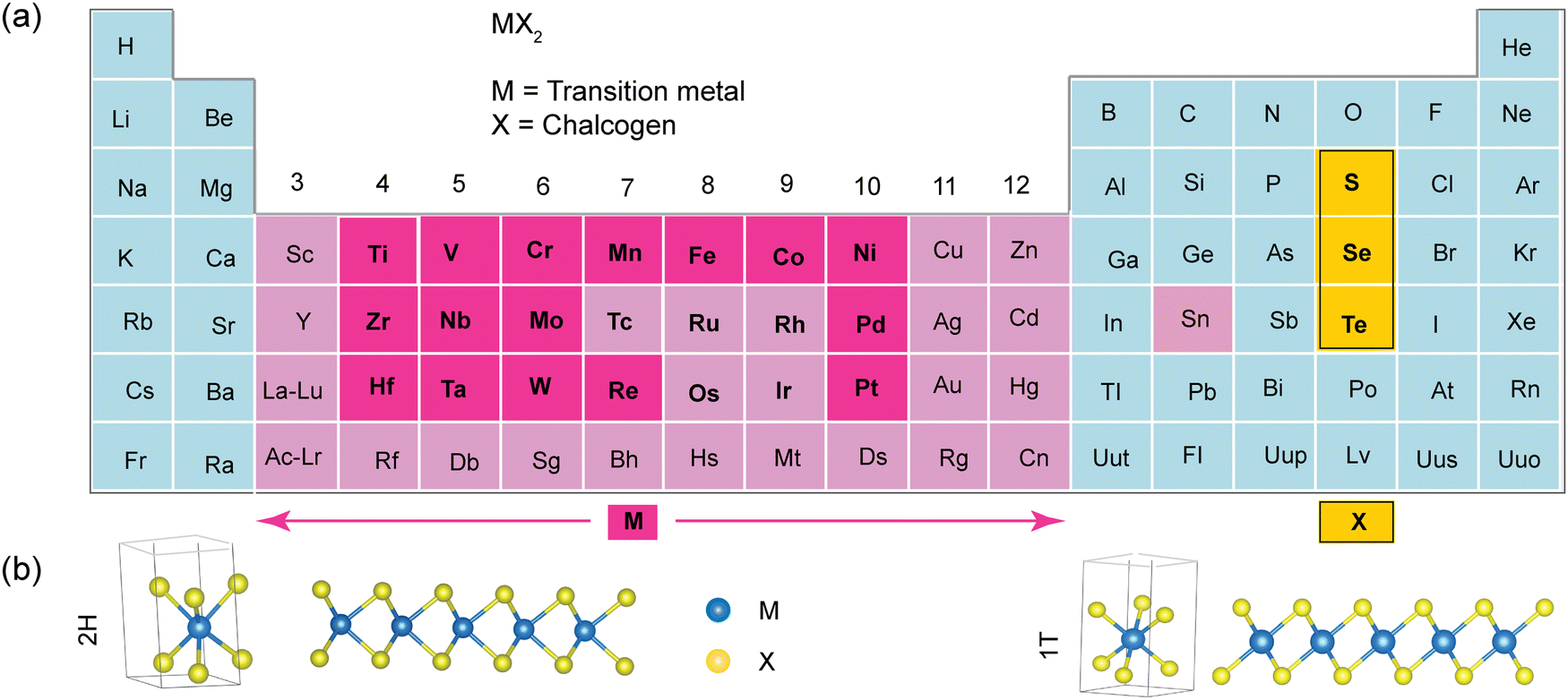 | ||
| Fig. 1 (a) A library of more than 50 distinct layered 2D TMD layered compounds. These compounds involve the transition metal (M) and the three chalcogens: sulfur (S), selenium (Se), and tellurium (Te), which are prominently featured in the periodic table. (b) Top and side views of the schematic of monolayer MX2 (MoS2) with hexagonal (1H) and tetragonal (1T) symmetries. | ||
Transition metal atoms contribute four electrons to bond with chalcogen atoms, resulting in oxidation states of +4 for M and −2 for X. Chalcogen atoms’ lone-pair electrons stabilize the layer surfaces, preventing reactions with the environment. The distance between M–M bonds varies depending on the metal and chalcogen size. An MX2 monolayer can exist in three phases: 1T, 2H, and 3R, representing different layer counts and symmetries (Fig. 1b). The numbers of X–M–X (S–Mo–S) units represents the number of layers in the unit cell and the letters indicate symmetry (T: trigonal; H: hexagonal; and R: rhombohedral).4
1.2. Diversity of TMDS
The MX2 family exhibits diverse electronic properties, ranging from insulators such as HfS2 to semiconductors such as MoS2 and WS2 and even metals/semimetals such as VSe2, PdSe2, TiSe2, NbS2, CrS2, and TaS2.5–9 However, this review places an emphasis on TMD semiconductors with bandgaps around 1–2 eV, with a particular importance on MoS2, WS2, MoSe2, and WSe2. MoS2 has three structural phases: 1T (metallic), 2H (semiconducting), and 3R (semiconducting). External stimuli or chemical treatments can induce structural phase transitions, making MoS2 a versatile material for different applications. For instance, when immersed in n-butyl lithium, MoS2 has the capability to transition from its semiconducting 2H phase to the metallic 1T phase.2Recently, the investigation of heterojunctions involving atomically thin 2D materials, specifically transition metal dichalcogenides and organic molecules, has emerged as a rapidly expanding field of scientific and technological exploration. The primary objective behind studying these TMDO heterojunctions is to comprehend and harness the distinctive characteristics of their constituent materials, as well as the novel properties that arise from their synergistic combination. When envisioning the attributes of interfaces between dissimilar materials including TMDO heterojunctions, the initial approach often involves simplifying the system into a band energy level diagram. In a TMDO heterojunction, the relevant energy levels encompass the highest occupied molecular orbital (HOMO) and the lowest unoccupied molecular orbital (LUMO) relative to the TMD material valence band maximum (VBM) and conduction band minimum (CBM), respectively. By examining this alignment of energy levels, one can anticipate the flow of charges in both ground and excited states. The substantial hybridization of p- and d-orbitals in the TMDO system near the Fermi energy profoundly influences band alignment and charge transfer at the interfaces, thereby enabling the fine-tuning of the electronic structure and photoluminescence (PL) characteristics of TMDs.10,11 Consequently, this methodology is frequently employed to identify the potential combinations of TMDO materials suitable for applications such as photovoltaic cells, photodetectors, diodes, and various electronic and optical devices.
However, the model of energy level alignment does not fully encompass many of the pertinent details associated with the TMDO heterojunction. For instance, the proximity of a molecule to the TMD material can induce shifts in the energies of bands and orbitals via the electrostatic and hybridization effects. Moreover, apart from the primary HOMO and LUMO, other molecular orbitals have the potential to contribute to the photophysical dynamics observed in the TMDO heterojunction. Additionally, in the heterojunction, electrons and holes may not exist as free carriers but instead primarily manifest as bound electron–hole pairs, resulting in a range of distinct physical phenomena. The simplistic energy-level alignment approach also fails to account for details pertaining to magnetism or the molecular spin states, molecular orientation, thin-film morphology, and chirality. These extra molecular characteristics provide significant opportunities for further modulation of the properties of TMDO heterojunctions.12 As a result, the combination of transition metal dichalcogenides and organic semiconductors in heterostructures provides a versatile platform for the exploration of novel optical and electronic properties in multifunctional devices. This is due to the occurrence of unique physics at the interfaces of TMDO. Furthermore, various TMDO heterostructures showcase improved optical and electrical performance when compared to individual TMD layers or organic entities.13,14 From an application perspective, both 2D-TMDs and organic semiconductors are in high demand for the development of next-generation flexible and wearable electronics, chemical/biological sensors, detectors, displays, and related technologies. The combination of the efficient light absorption capabilities of organics with the high carrier mobility of inorganics holds the potential to enable cost-effective and efficient optoelectronic devices. Unfortunately, the optoelectronic properties of TMDO heterojunctions and TMDs doped with organic molecules have not yet been fully exploited and the underlying physics is still not well understood. Studying heterojunctions and the effects of doping can play a crucial role in determining the function of hybrid systems. Thus, incorporating 2D-TMDs with organic semiconductors would lead to a plethora of opportunities to modulate the optoelectronic properties and different unusual physical and chemical properties that have not been realized before. In addition, the atomic-scale control of organic molecular arrangements on recently reported TMDO interfaces has been found not well controlled. This limitation is noteworthy since the optoelectronic characteristics of organic molecular crystals depend significantly on their aggregation and molecular configurations.14,15 This review provides an overview of the ultrathin and well-controlled molecular arrangements on the interface through various synthesis techniques and explores how the molecular aggregations would affect the light–matter interactions in the hybrid heterostructure system. Typically, very thin organic molecular layers with a thickness less than 5 nm have a clean interface and high excitonic densities, accompanied by high binding energies. These distinctive properties enable them to effectively interact with excitonic states in TMD materials. As a result, TMDO heterostructures hold great potential as viable candidates for the development of optical devices including photodetectors and light-emitting devices.16
In addition to that, organic molecules have compatible features with TMDs. The technologies based on many novel applications are challenging because of demands such as large-area coverage, optical transparency, flexibility, and easy processing. Here, combining organic semiconductors with TMDs can fulfill the desired requirements, as organic semiconductors can be deposited by simple fabrication at low temperatures on almost any substrate. Furthermore, this offers a vast array of functions, from memory switching, wide range absorption (visible to far-infrared), light emission, to chemical/biological light-sensors, and photodetectors. Organic molecules have large charge carrier effective masses, and low dielectric polarizability compared to traditional inorganic semiconductors. Therefore, TMDO materials would be established with improved or unusual novel physical as well as optoelectronic properties. TMDs sometimes show intrinsic volatile-chalcogen (S, Se, and Te) vacancies; however, by doping the TMDO heterostructure, the vacancy sites can be reduced, and the optoelectronic properties can be remarkably modulated. It can be noted that despite the vdW interaction, the vdW interfaces are extremely complex and poorly defined in cases when they are buried by the over layers, making it hard to quantify the active junction sites and the physical properties such as those in field-effect transistors (FETs). To resolve this issue, we can use atomically thin TMDs to make TMDO heterostructures, which eliminate all unwanted vdW junctions. Organic layers alone often show amorphous grains in the active channel, and as a result, the transport properties are always realized from hopping and not from band transport.17
1.3. Types of organic compounds incorporated with TMDs and their requirements
Combining organic layers with 2D TMDs is an area of active research with various applications including electronic devices, detectors, and sensors. The choice of organic layer depends on the specific application and the desired properties. Here are some examples of organic molecules that can be combined with 2D TMDs and their requirements: (i) organic semiconductors: organic semiconductors can be combined with semiconducting 2D TMDs to create heterostructures. The choice of organic semiconductors should match the electronic properties and band energy alignment (type-I/II/III) of the TMD. For example, interlayer exciton (ILX) emission, a type-II band energy alignment with the p–n junction, is necessary, where the organic semiconductor could be p-type and the TMD be n-type (vice versa). Similarly, this p–n junction and ILX emission concept is also applicable for other TMD/organic semiconductors.13,18,19 Again, for lasing, giant PL emission enhancement type I is needed.14,20 Moreover, these heterostructures find application in electronic and optoelectronic devices including field-effect transistors (FETs) and photodetectors. (ii) Organic ligands: organic ligands are commonly used to functionalize the surface of 2D TMDs. These ligands can be small molecules or polymers with functional groups (e.g., amines, thiols, and carboxylic acids) that can chemically bind to the TMD surface.21,22 Organic ligands can improve the dispersibility of TMDs in solvents, enhance stability, and provide specific chemical functionalities for targeted applications. (iii) Polymer matrices: polymers with good solubility and compatibility with TMDs are often used to form 2D layered structures. These polymers should have functional groups that can interact with TMDs via non-covalent interactions or covalent bonding. Polymer-TMD composites are used in flexible electronics, coatings, and membranes, where the polymer matrix can provide mechanical support and enhance material properties. (iv) Organic dyes: organic dyes can be used for PL studies when combined with TMDs. The absorption and emission properties of the organic molecules should complement the TMD's properties. This combination is used in PL spectroscopy and imaging to study the electronic and optical properties of TMDs.23 (v) Conjugated polymers: conjugated polymers can be combined with TMDs to create hybrid materials with unique electronic properties. The polymer should be chosen to match the TMD's electronic band alignment whether type I, type II, or type III. These hybrids find use in photovoltaics, light-emitting transistors, and other organic electronics.24–28 In all the cases, the choice of organic molecules should consider their compatibility with the 2D TMD surface, the intended application, and the desired chemical and physical properties of the resulting composite material. Surface functionalization techniques such as chemical modification or physical adsorption are often employed to achieve the desired interactions between organic molecules and 2D TMDs.1.4. Importance of band alignment in determining device performance
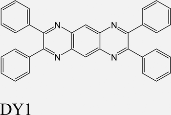
The band alignment (Type-I/II/III) between transition metal dichalcogenides (TMDs) and organic materials at heterojunctions is of paramount importance for determining the performance of various electronic and optoelectronic devices. The impact of band alignment on device performance in TMD/organic hybrid systems can be summarized as follows: (i) efficient charge transport, (ii) reduced energy barriers, (iii) enhanced photoemission, (iv) tunable emission, (v) enhanced sensing performance, and (vi) quantum confinement effects. For example, a resonance energy transfer (RET) from a red-emitting monolayer WS2 (1L-WS2) to a layer of NIR-emitting organic dye molecule–based type-I heterostructure.29 It is found that the total PL yield of the heterostructures is up to a factor of eight higher than the PL yield of pristine 1L-WS2. A strong decrease in the PL of the dye is observed on 2L-WS2 when it gives the type II heterostructure. A PTCDA/MoS2 type I heterostructure results in enhanced PL emission.20 Again, the PL emission spectra of the DY1/MoS2 type I heterostructure reveal the quenching of DY1 emission and the enhancement of MoS2 emission. This observation points to a robust electronic interaction between these two materials.30 In type II, in particular p–n junction, TMDO heterostructures, generally the PL emission peak quenches for individual layers; however, recently an extra ILX emission peak from the NIR to IR range has been observed. Due to their spatially indirect nature, interlayer excitons possess long-lifetimes, attributed to the reduced overlap between electron and hole wavefunctions,31,32 extended spatial coherence of the excitons,33 quantum emitter,34 and high-temperature exciton condensate.35,36 Most recently, Thompson et al., has unveiled, in both theoretical models and experimental observations, distinct features of the entire intra- and interlayer exciton landscape in the PL spectra. In particular, Notably, they have identified a significant transfer of intensity from the intralayer TMD exciton to a series of energetically lower interlayer excitons with decreasing temperature.19 Nevertheless, it is worth noting that type III alignment has not been reported thus far, and its occurrences in 2D/2D heterostructures are relatively scarce. An artificial neural network simulation, utilizing electronic synaptic arrays and trained on handwritten digit datasets, showcased an impressive recognition accuracy of 91.3%.37 However, the organic layer could fill the gap in near future. Therefore, the careful engineering of band alignment between TMDs and organic materials is fundamental for optimizing the performance of hybrid electronic and optoelectronic devices. It facilitates efficient charge transport, reduces energy barriers, enhances light emission, and allows for the tailoring of energy levels to meet the specific needs of diverse applications, ultimately leading to improved device functionality and efficiency.This review overviews the most recent advent in two-dimensional transition metal dichalcogenide/organic-enabled interlayer exciton emission and emission modulation covering a range of 2D-TMD materials and organic layers and how the band energy alignment affects it. We discuss the suitability of 2D-TMDO material properties for synaptic devices. Their operational principles are thoroughly examined, and this is followed by the presentation of up-to-date device applications, encompassing field-effect transistors, detectors, and phototransistors. In this review, we initially present the remarkable characteristics exhibited by different TMDs and organic semiconductors (molecules and polymers), and we explore the emerging applications enabled by TMDO hybrid heterostructures in Section 1. In Section 2, we highlight some physical and chemical synthesis routes and fabrication processes using various experimental techniques for 2D-TMDs and organic layers, either individually or for hybrid heterostructures. We also outline the challenges and propose ways to improve the experimental techniques for TMDO hybrid heterostructure fabrication. In Section 3, we provide the band energy alignment schemes of various TMDs with respect to a library of organic molecules and polymers. We also discuss the various types of band alignment, namely, type I, type II, and type III. We discuss the band bending and charge transfer processes in the TMDO heterojunction system from the perspective of band structure and molecular orbital theory. In Section 4, we provide well-comprehensive discussions about the most recent breakthrough in the novel room-temperature interlayer exciton emission and its modulation in the TMDO hybrid heterojunction. Unlike the typical TMD-TMD heterostructure, the TMDO system is usually far from lattice matching. In this section, we highlight the up-to-date research progress in the modulation of emission signals in TMDO constituents from the perspective of photoinduced charge transfer, energy transfer, doping, defect healing, and phase engineering. In the main context, we include a table summarizing molecular structures with the HOMO/LUMO level, type of band alignment, and advancement of emission response of diverse TMDO hybrid heterostructures. In addition, we also discuss the emission modulation in the hybrid structure beyond the band energy alignment. Next, in Section 5, we overview the recent progress in 2D-TMDO material–based optoelectronic synaptic devices for neuromorphic applications, covering an array of 2D-TMDs and organic materials, which are investigated for them. The 2D-TMD and organic material property compatibility for the synaptic devices is discussed, and their operating principles are revisited, followed by the current device demonstrations. We also present, in detail, the advancement of the performances of field-effect transistors—a key component of integrated electronic circuits, anti-ambipolar transistors, phototransistors, and a contemporary breakthrough—photo-switchable superlattices. We summarize the up-to-date research on improved FET performances including organic doping, phase engineering, and hybrid heterostructures in a table within the main context. In section 6, we highlight one of the real-life applications—the photodetectors based on TMDO hybrid heterostructures. In addition, we pinpoint the present challenges and possible solutions for TMDO detectors. Finally, in Sections 7 and 8, we conclude this review by outlining the current challenges from synthesis to device applications and outlooks on this topic of emerging TMDO heterostructures.
Recently, a review article has been published on the recent advances in 2D organic–inorganic heterostructures. It focuses on the integration of 2D organic materials with 2D inorganic materials, emphasizing the combination of organic and inorganic layers, synthesis techniques, and the importance and range of device applications including FETs, photodetectors, solar cells, and neuromorphic computing devices. We include this information in the review article with proper citation.38
2. Fabrication of TMDO heterostructures
The morphology and molecular orientation within TMDO heterojunctions are influenced by the specific fabrication techniques employed. Typically, the fabrication process involves initially creating a film of TMD material, followed by the deposition of the organic layer on top (or vice versa, such as in the case of self-assembled monolayers—SAMs).39,40 The choice of the preparation method for the 2D-TMD material is generally made based on the intended application and the characteristics of the substrate. Thin-film fabrication methods for TMDO hybrid materials can be broadly classified into two categories: solution-phase and gas-phase film deposition. Solution-phase techniques include drop casting, spin coating, blade coating, and printing. In this context, several common approaches for fabricating TMDs and organic layers are briefly discussed.2.1. Mechanical transfer (top-down method)
Top-down methods, commonly known as exfoliation techniques, are utilized to isolate single or a few layers of transition metal dichalcogenides (TMDs) from bulk crystals (see Fig. 2a). These methods encompass mechanical exfoliation conducted under ambient conditions or in an inert atmosphere, and chemical or electrochemical exfoliation performed in a liquid phase. By stacking mechanically exfoliated monolayer flakes, various TMDO heterostructure (transition metal dichalcogenide/organic) materials can be synthesized. The procedure commences with the exfoliation of TMD flakes onto an ultra-soft viscoelastic polydimethylsiloxane (PDMS) stamp via mechanical exfoliation aided by high-quality Nitto tape. Subsequently, the PDMS stamp, with the flakes facing away from the glass slide, is affixed to a desired glass substrate, and optical microscopy is employed to align the flakes with the target substrate. Via controlled manipulation using a manipulator, the flakes are gently brought into contact, after which the glass slide is gradually elevated, resulting in the separation of the TMD flakes from the PDMS stamp and their specific positioning on the substrate.41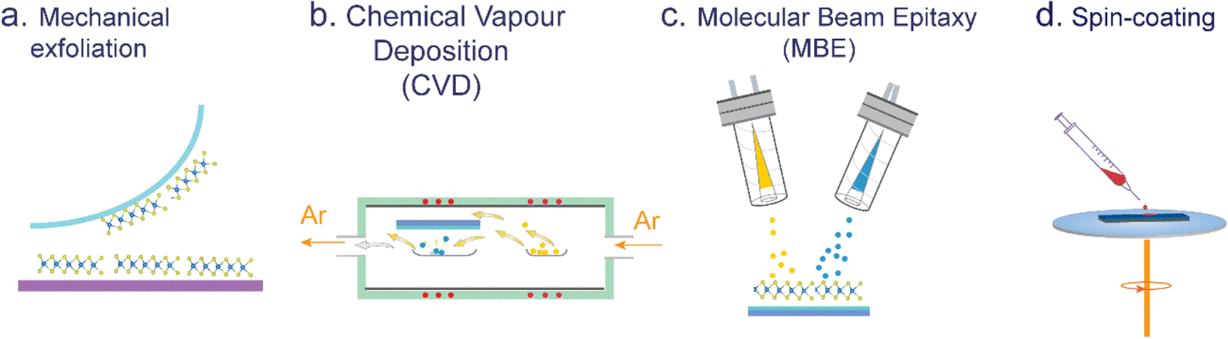 | ||
| Fig. 2 Commonly used techniques for TMDO synthesis: (a) exfoliation, (b) chemical vapor deposition (CVD), (c) molecular beam epitaxy (MBE), and (d) spin-coating. | ||
Moreover, mechanical exfoliation has demonstrated its effectiveness in producing high-quality monolayers of transition metal dichalcogenides (TMDs). Although extensively employed in fundamental research and fabrication, this method is primarily utilized for concept testing in a limited number of heterostructure-based devices. It is accompanied by certain limitations such as small flake sizes, variations in layer thicknesses, and low production throughput. Consequently, there is a growing demand for scalable approaches that enable precise control over the lateral size and thickness of TMD layers, ensuring excellent reproducibility for practical applications. Chemical vapor deposition (CVD) growth methods are commonly employed to generate large-area TMD crystals, effectively addressing the scalability requirements for practical implementation.
2.2. CVD (bottom-up method)
Since the exfoliation method tends to yield relatively small flakes, direct growth methods are employed in certain applications that require large-area 2D films. Therefore, utilizing bottom-up techniques enables the direct synthesis of TMD layers onto a desired substrate, provided that the substrate possesses a high melting temperature, such as SiO2, sapphire, or mica.42 Presently, the chemical vapor deposition (CVD) technique stands as a widely employed method for synthesizing 2D TMDs (see Fig. 2b). Later developments enabled the synthesis of micro- and millimeter-sized single-crystal TMD domains. Similarly, CVD is among the most popular means of preparing TMDs with controlled stoichiometry, layer number, grain boundaries, and domain size. The CVD method can be categorized into two distinct ways—the ‘single-vapor zone’ method, also known as the sulfurization method, and the ‘double vapor zone’ method. The ‘single vapor deposition’ method involves the initial deposition of transition metal precursors onto the substrates. Subsequently, through the introduction of controlled heat treatment within an environment of sulfur vapor, these active precursors undergo a series of controlled chemical reactions, resulting in the formation of TMD layers. This approach is commonly employed to synthesize TMD layers with precise control over their composition and morphology. In the ‘double-vapor zone’ method, an inert gas is utilized to transport both the vapor states of transition metal precursors and chalcogens (sulfur or selenium or tellurium) in the tube. This gas flow facilitates deposition onto the target substrate, under controlled thermal treatment. This process, occurring within the realm of physics, enables controllable reactions and transformations, ultimately leading to the synthesis of desired materials with specific compositions and properties. In the ‘double vapor zone’ method, both transition metal precursors such as molybdenum oxide and tungsten oxide and chalcogen precursors such as sulfur, selenium or tellurium in their vapor states are carried by the inert gas flowing in the tube onto the target substrate under thermal treatment. Volatile precursors such as MoO3 and S are co-evaporated and then reacted to form the desired TMD deposits (e.g., MoS2) on the surface of specific targeted substrates. In a particular investigation, Kang et al. achieved the successful fabrication of single-layered films of MoS2 and WS2 on 4-inch silicon oxide wafers. To achieve this, they utilized Mo(CO)6 and W(CO)6 as transition metal precursors, while (C2H5)2S was selected as the sulfur precursor.43 A detailed description of typical CVD precursors and growth conditions utilized for TMDs is given in topical review articles.42,44 In addition, several variations of the CVD method have been demonstrated. In summary, the CVD process has emerged as a highly effective and preferred technique for the large-scale synthesis of high-quality monolayers and multi-layers of various 2D TMDs. This method has proven in achieving precise control over the growth of TMD structures, enabling the production of extensive areas of TMD films with exceptional quality. In theory, the powder-based CVD growth of MoS2 involves a sequence of thermal and chemical processes, which can be represented using the following chemical reaction equations:45| 2MoO3 + xS → 2MoO3−x + SO2 | (1) |
| 2MoO3−x + (7 − x)S → 2MoO2 + (3 − x)SO2 | (2) |
| 2MoO3 + 7S → 2MoS2 + 3SO2 | (3) |
2.3. MBE: a novel approach to high-temperature TMD synthesis
Subliming molecular precursors using a molecular beam epitaxy (MBE) or an organic molecular vapor deposition (MVD) method (see Fig. 2c) onto a substrate offers the possibility of generating ultraclean interfaces, and the thickness of the active layer can be monitored exactly, e.g., by using a quartz crystal microbalance.48–53 Several growth parameters can be fine-tuned to engineer the layer growth (e.g., substrate type, deposition time and sublimation temperature), offering the possibility to precisely control the film morphology.54,55 MBE was successfully applied to grow a variety of TMDs; however, the main disadvantage of this technique is that it is relatively expensive, slow, and requires rather cumbersome equipment for maintaining ultra-high vacuum. However, the MVD method allows for the evaporation of a majority of organic molecules without requiring ultra-high vacuum conditions, as these molecules generally do not decompose before reaching their sublimation temperature. The ultraclean and highly controllable interfaces grown via sublimation are well suited for investigating various underlying physical processes concerning interfaces.13,14Further, MBE is a versatile method that simplifies precursor development for 2D materials, particularly complex 2D ferromagnetic materials like FGT.56 It uses physical vapor deposition (PVD), and refractory metals such as Mo, W, Cr, Fe, and Co are vaporized.46,57 However, magnetic metals can cause scattered evaporation beams. An alternative is using high-temperature (above 850 °C) effusion cells, but it increases thermal load and contamination risks. MBE plays a crucial role in the synthesis of CrTe2 and CrxTey 2D-ferromagnetic materials since many of these compositions naturally adopt a quasi-2D structure, primarily because of significant self-intercalation of Cr.58 It is also ideal for creating heterostructures with other 2D materials, essential for spintronic devices. The ultrahigh vacuum environment for MBE allows monitoring growth in situ using various surface characterization techniques, setting it apart from other methods like CVD. It is also attractive that MBE, being a UHV technique, allows for the in situ monitoring of the growth of 2D materials by a number of surface sensitive characterization techniques such as electron diffraction, low-energy electron diffraction (LEED), reflection high-energy electron diffraction (RHEED), scanning tunneling microscopy (STM), X-ray photoelectron spectroscopy (XPS), and angle-resolved photoemission spectroscopy (ARPES), which cannot be applied when any other growth methodology (e.g., CVD) is used.
2.4. Spin-coating
Spin-coating is a widely adopted method to form homogeneous films extending over large areas onto TMDs supported on a substrate.59–63 The spin-coating process involves depositing a solution containing the desired molecules onto the center of a rotating substrate, which supports the TMDs (see Fig. 2d). Through a carefully optimized rotational speed, the solution is uniformly spread across the entire surface. Generally, a low boiling point solvent is employed, in some cases followed by an annealing step to eliminate the remaining solvent residues. In contrast to drop-casting and dip-coating techniques, spin-coating offers the advantage of producing uniform films whose thickness can be precisely adjusted by optimizing parameters such as the molecular concentration of the solution, the boiling point of the solvent, and the rotational speed.64 Nevertheless, being a kinetically driven process, spin-coating does not give a high quality of structural order at the molecular level.2.5. Drop-casting
Drop-casting is considered perhaps one of the most straightforward techniques for producing a 2D TMDO interface, and it has found application in several works. Generally, a drop of solution is applied onto the TMD crystal that has been exfoliated or CVD-synthesized on a selected substrate. Subsequently, the solvent is allowed to evaporate slowly.65,66 For this approach, volatile solvents are often employed, and mild thermal annealing is sometimes used to facilitate solvent evaporation. The resulting films from drop-casting are usually non-uniform due to the influence of largely uncontrollable surface-dewetting and solvent evaporation dynamics, which lead to material accumulation at the droplet edges. However, the interface between a drop cast film and a TMD is not necessarily disordered, as the nanoscale molecular arrangement depends on the molecule and TMD involved. For instance, the drop-casting of long alkanes on 2D TMD layer results in highly ordered epitaxial films.40 Unfortunately, not every molecule, but some small molecules, displays an adequately high solubility in common solvents (e.g., toluene, acetone, hexane, and 2-propanal). For example, perylene, pentacene, and metal phthalocyanine molecules are not soluble in common solvents. Hence, most small molecules are substituted by many groups to be soluble in the usually available solvents.2.6. Dip-coating
Dip-coating serves as another widely employed and extremely practical method to fabricate TMDO interfaces.21,65–69 TMDs supported on a substrate are immersed into a solution, where molecules interact with the TMD surface and impart the desired functionality. Specifically, dip-coating is typically associated with a scenario in which the substrate is immersed into the solution and quickly removed, but soaking refers to the situations in which the substrate remains immersed for some time. In both cases, low–boiling point solvents and gentle annealing are frequently used to achieve solvent-free molecular films. In contrast to the drop-casted molecular film, dip-coated layers are generally very thin, as often only molecules in direct contact with the sample surface become attached to it, while others remain in the solution. Therefore, dip-coating creates molecular monolayers, or even sub-monolayers. Interestingly, it is sometimes found that keeping the TMD immersed in a solution, and mixed with alkane or thiol for a longer time results in a considerable effect on its electronic properties. This phenomenon can be explained by considering that more molecules have time to interact with the ultra-flat TMD surface and impart their functionality.2.7. Langmuir–Blodgett deposition method
The Langmuir–Blodgett (LB) technique is one of the important and widely employed methods for the fabrication of ultra-thin ordered 2D molecular structures.70–73 Because the orientation, packing, and long-range structure of each individual layer can be finely adjusted with meticulous precision, it becomes possible to manipulate the thickness and uniformity of the films at the molecular scale. As an example, Ponomarenko et al. employed the LB technique to fabricate an oligothiophene derivative (D2-Und-4 T-Hex).73 The formation mechanism of a uniform 2D monolayer on the air–water interface involves closely self-assembled molecules via intra-molecular π–π stacking interactions. To deposit a single layer via the LB method, the substrate must be placed at an air–water interface prior to cleaning and spreading the material, so that it only needs to be ‘pulled’ through the interface once. Before placing an SiO2 substrate, it must be cleaned with acetone and isopropyl alcohol for a few minutes, dried with N2, and then subjected to oxygen plasma for several minutes. This process endows the substrate with the hydrophilic nature needed to form MoS2, which is also hydrophilic.74,75 In general, amphiphilic molecules, which contain both hydrophilic and hydrophobic groups, are necessary as soluble materials to form TMDO hybrid materials. Chemical inertness to both organic materials and subphase water plays a crucial role, as it prevents the solvent from reacting with them. Before depositing the films, substrates must undergo hydrophobic or hydrophilic treatments, depending on the desired type of LB films’ preparation requirement. These characteristics could pose challenges to the progress of LB film technology in the optoelectronics field. Nevertheless, the LB technique remains an excellent approach for fabricating macroscopic MoS2 devices, offering the advantage of enabling deposition across an entire wafer when required.752.8. Inkjet printing
Various methods have been employed to deposit solution-processed TMDO hybrids onto desired substrates. Among these techniques, inkjet printing holds particular significance from both technological and industrial standpoints due to its capability to achieve low-cost production of large-area films. In all printing processes, including inkjet, screen, and roll-to-roll printing, the ink formulation plays a key pivotal role that fundamentally controls the physical properties of the deposited films. Molecules and polymers are commonly incorporated in TMD dispersion to make functional inks with the desired rheological properties, which have been used to fabricate rudimentary memory elements and photodetectors. Consequently, they present an opportunity to incorporate additional functionalities into CMOS (complementary metal-oxide-semiconductor) technology, following the more-than-Moore approach.76–782.9. Other important parameters, and the effect of temperature, pressure, gas flow rate, substrate interface property, and organic moiety
Substrate interface property. (i) Effect on surface structure: substrate properties, such as lattice mismatch and surface energy, can influence the nucleation, growth orientation, and stacking of TMD layers on the substrate. Epitaxial growth on specific substrates can result in ordered surface structures.90 (ii) Effect on chemical composition: the interaction between TMDs and substrates can impact surface chemistry, potentially leading to surface reconstruction or modification.
Precursor delivery. Precursor delivery methods including gas-phase precursors or liquid-phase precursors in solutions can influence the growth mechanisms and surface kinetics, affecting the surface structures and layer stacking. The choice of precursor molecules and their delivery rates can directly impact the chemical composition of TMDs. Thus, controlling precursor delivery is critical for stoichiometric control.
3. Energy band alignment TMDO
3.1. Band energy formation in TMDO hybrid heterostructures
In the realm of two-dimensional materials, a substantial number of 2D TMD layered compounds are present (see Fig. 1).2 A library of molecules and key TMDs, with MoS2 band energies as reference, are depicted in Fig. 3. In bulk, 2D-TMDs exhibit an indirect bandgap with many-body interactions that facilitate the features of their optoelectronic properties. However, many 2D-TMDs have a direct bandgap in the form of a monolayer, exhibiting a noticeable photoluminescence emission (see Fig. 5b and c).119,120 Furthermore, much underlying physics can be found by considering the band-alignment, strain effects, doping levels, and manipulation of the surrounding active layer (or dielectric environment). These considerations provide ample scope for implementing heterostructure engineering based on TMD layers. The hybridization of d-orbitals of the transition metal atom (dz2, dx2−y2, dxy) and the p orbitals of the chalcogen atom (px, py) in TMDs gives rise to the formation of the conduction band minimum, CBM (dz2; px, py), and valence band maxima, VBM (dx2−y2; px, py), respectively (see Fig. 5a).93 These bands, CBM and VBM, play a significant role in band bending and charge transfer occurring across the heterointerface to the highest occupied molecular orbital (HOMO) level and lowest unoccupied molecular orbital (LUMO) level of the organic molecule within the TMDO heterostructure. Subsequently, the modulated light emission directly influences the 2D-TMD-based optoelectronic devices. It is interesting to note that the weak TMDO interactions enable the organic molecules to self-assemble according to the vdW weak intermolecular interactions. The vdW interactions between the TMD material and the deposited organic layer result in the molecular packing behavior within the first few overlayers. Importantly, thanks to their ultrahigh surface sensitivity, the optical and electrical characteristics of TMDs can be modified by a physisorbed ad-layer, without the need for strong chemical bonds.13,14 A collection of molecules and some essential 2D-TMDs with their band energies are illustrated in the schematic in Fig. 3, where the relevant band energies of MoS2 are taken as a reference. However, further theoretical investigations of these materials are essential to identify promising atomic heterostructures suited for specific device applications, depending on the field of usage.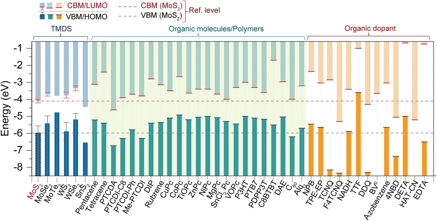 | ||
| Fig. 3 Band energy diagram of a few key TMDs, organic molecules, and polymers (abbreviations are mentioned in Table 1). The horizontal red (CBM) and black dotted line (VBM) refer to the MoS2 energy levels.1,13,14,16,25,39,48,59,67,93–118 | ||
3.2. Type of band alignments in TMDO hybrid structures and their impact on properties
Typically, in semiconductor heterostructures, the band alignment can vary based on the disparity in energy between the conduction and valence band extrema within the constituent layers (schematic representation in Fig. 3). The classification of heterojunctions into three distinct types, namely, type I (symmetric/normal gap), type II (staggered gap), or type III (broken gap), is determined by the relative positions of the CBM or LUMO, and the VBM or HOMO within the constituent layers of transition metal dichalcogenide/organic heterostructures. Fig. 4 visually presents the schematic representation of these different heterojunction types—type I, type II, and type III based on the band energy positions. These heterojunction types are distinguished based on the alignment of band energies, offering a range of opportunities for harnessing diverse functionalities within modern electronic and optoelectronic devices.121 In the context of heterostructures, the lowest-energy states for electrons and holes exist in the same layer in case of a type-I heterostructure. Conversely, for a type-II heterostructure, these lowest-lying states are segregated into distinct layers. This distinction in the spatial arrangement of electron and hole states in different heterostructure types carries important implications for their electronic and optical properties. Moreover, the band energy offsets of TMDO may result in a reduction of lower the CBM of one layer, potentially positioning it below the HOMO of the other layer (a similar effect may occur when considering the VBM of one layer and the LUMO of the other layer). This energy alignment leads to the formation of a type-III heterostructure.122,123 Under type-I TMDO band alignment, photogenerated electrons and holes effectively undergo transfer from the active material characterized by a larger bandgap to the smaller bandgap. This process results in the spatial confinement of charge carriers in the layer with the lower bandgap and consequently enhances the carrier population, which may strongly influence the light emission properties of 2D-TMD.122 Type-I band alignments find extensive applications in optical devices, including light-emitting diodes (LEDs).16,94 Currently, investigations on type-I TMDO heterostructures and their associated optoelectronic properties are somewhat limited. To achieve efficient charge transfer, it is essential to create a staggered (type-II) energy level alignment at the TMDO interface, where sufficiently large energy offsets exist between the frontier molecular orbital levels and the valence and conduction band edges of the TMD semiconductor. These pronounced energy offsets are crucial in promoting effective dissociation of excitons in TMDO systems (see Fig. 4).16,124 It is useful for unipolar electronic device applications and photocatalysis. In other words, type-II staggered band alignment allows for the spatial separation of electrons and holes in the heterojunction in favor of various optoelectronic applications. In type-II heterojunctions, the structure confines electrons and holes into energy bands of different layers, hence leading to the implementation of a high-mobility transistor.121,125,126 Within a type-II heterostructure, electrons accumulate in the layer with the lower CBM, whereas the holes accumulate in the layer with higher VBM. Nonetheless, energy transfer can still occur between the larger bandgap material to the smaller band gap material.122 Recent experimental studies have reported significant energy transfer phenomena in type-II heterojunctions based on TMDs.127,128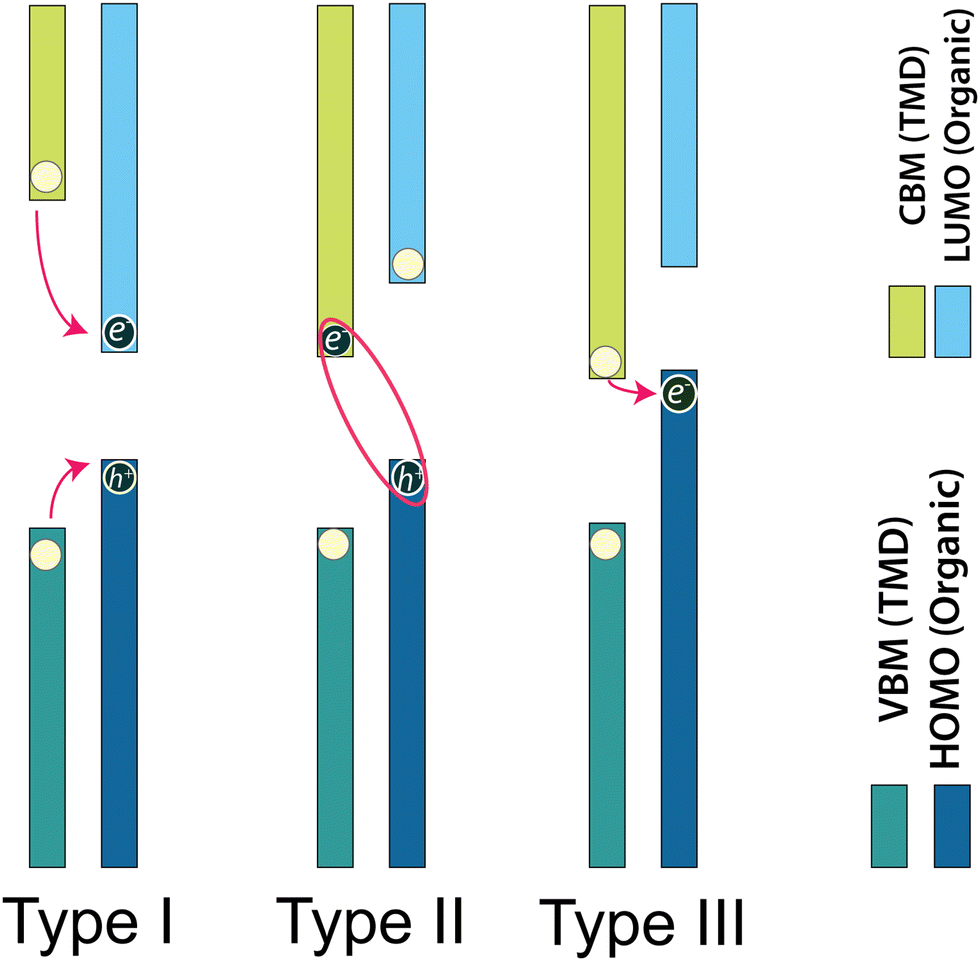 | ||
| Fig. 4 Illustration showing the generalization of band alignment: type-I (normal), type-II (staggered gap), and type-III (broken gap) semiconducting heterostructures. The band colors green and blue (lower panel) represent the VBM of TMDs and the HOMO of organic materials, respectively, while light green and sky-blue (upper panel) represent the CBM of TMDs and the LUMO of organic materials or vice versa, respectively. | ||
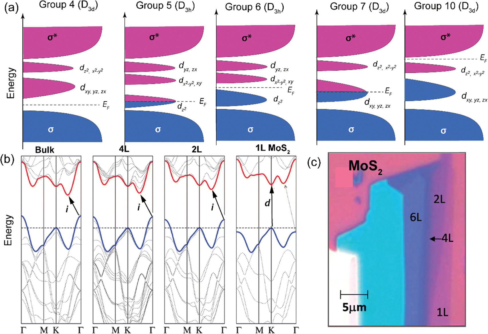 | ||
| Fig. 5 (a) d-Orbital filling and electronic character of various TMDs. Schematic illustration showing the progressive filling of d orbitals that are located within the bandgap of bonding (σ) and anti-bonding states (σ*) in TMDs. The filled and unfilled states are shaded with dark and light blue, respectively. (b) Calculated band structures of bulk to 1L MoS2. The bold black arrows indicate the lowest energy transitions. (c) Microscopic image of MoS2 flakes displaying different contrast corresponding to MoS2 flakes of diverse thicknesses. (b) and (c) Reproduced from ref. 120 with permission from American Chemical Society, copyright 2010. | ||
Type-III heterojunctions are also very useful for precisely tailoring the transition energy from the conduction band to the valence band. This is particularly crucial in tunneling FET, infrared lasers, and photodetectors.129 The stronger charge transfer in type-III heterostructures enhances the magnetic proximity effect and the coulombic interaction between the molecular layer and the TMD to enhance the valley splitting. This implies more opportunities to find large valley splittings in type-III vdW heterostructures.121,130
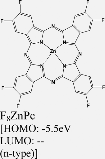
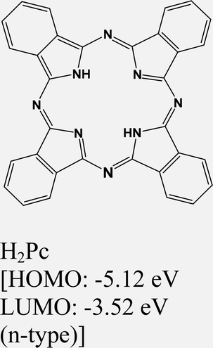
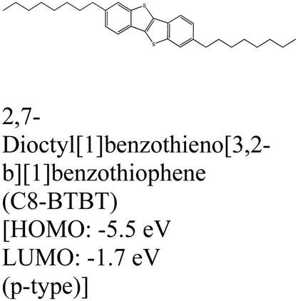
| Organic molecule/polymer (energy level; type) | TMD | Device processing & type of band alignment | Optical properties (PL) (emission, λmax) | Ref. |
|---|---|---|---|---|
| VD = vacuum deposition, UHV = ultra-high vacuum, CVD = chemical vapor deposition, MBE = molecular beam epitaxy, PVT = physical vapor transport, DP = dip-coatinga For TMDO band energy alignment, see the schematic in Fig. 3. | ||||
|
MoS2a | VD & type-II | Quenched (λmax = 710 nm) | Homan et al., 2017131 |
| N. A. Shen et al., 2017,132 | ||||
| Dong et al., 2017133 | ||||
| Ren et al., 2017,134 | ||||
| Jariwala et al., 201697 | ||||
| Black et al., 2023135 | ||||
| MoSe2 | VD & type-II | Enhanced (λmax = 788 nm) | L. Zhang et al. 2018,16 | |
| HfS2 | TD & type-II | — | K. Jung et al., 2020121 | |
| PtSe2 | UHV | — | Lin et al., 2017136 | |
|
WS2 | VD & type-II | Enhanced (λmax ≈ 740 nm) | Zhu et al., 201818 |
| WSe2 | TD & type-II | Quenched (λmax ≈ 760 nm), ILX emission ∼1.71 eV | L. Ye et al., 2021137 | |
| Thompson et al., 202319 | ||||
|
MoS2 | VD & Type II | Enhanced (λmax = 689 nm) | Obaidulla et al., 201914 Wang et al., 2018138 |
| Habib et al. 2018139 | ||||
| Rijal et al., 2020140 | ||||
| Rijal et al., 2023141 | ||||
| MoSe2 | TD & Type II | Quenched (λmax = 689 nm) | S. Park et al. 202120 | |
| J. Gu et al., 2018128 | ||||
| WS2 | VD & Type II | Quenched (λmax = 689 nm) | Z. Ye et al., 2014142 | |
| Liu et al., 201798 | ||||
|
MoS2 | PVT & type-II | Enhanced (λmax ≈ 700 nm) | H. Zhao et al., 2019100 |
|
MoS2 | VD & Type II | Quenched (λmax = 710 nm) | Obaidulla et al., 201914 |
|
MoS2 | OMVD | — | Mrkyvkova et al., 2019143 |
| MoS2 | VD & Type II | Quenched (λmax = 710 nm) | Yahya et al., 2020101 | |
|
MoS2 | PVT & type II | Quenched (λmax = 550 nm) | E. H. Cho et al., 2015144 |
| Fucai Liu et al., 20151 | ||||
| X. He et al., 201748 | ||||
|
MoS2 | VD & type II | Quenched (λmax = 550 nm) | Park et al., 201752 |
|
MoS2 | VD & type II | Quenched (λmax = 550 nm) | Kong et al., 202213 |
|
MoS2 | VD & type II | Quenched (λmax = 550 nm); ILX (≈805 nm) | Kong et al., 202213 |
| M. C. Schwinn et al., 2022145 | ||||
| Wang et al., 2023146 | ||||
|
MoS2 | Drop casting, vapor deposition & type II | Enhanced (λmax = 670 nm) | G. Ghimire et al., 2018147 |
| S Vélez et al., 2015102 | ||||
| S. H. Amsterdam et al., 201951 | ||||
|
MoS2 | Immersing | — | Y. Yang et al., 2020,69 |
|
MoS2 | Immersing | — | Kafle et al., 2016148 |
| Y. Yang et al., 202069 | ||||
| Y. Huang et al., 2018105 | ||||
|
MoS2 | Immersing | Enhanced (λmax = 660 nm) | Choi et al., 2016106 |
| MoSe2 | Immersing | Enhanced (λmax = 790 nm) | ||
| WSe2 | Immersing | Quenched (λmax = 750 nm) | ||
|
MoS2 | Immersing | Enhanced (λmax = 660 nm) | Choi et al., 2016106 |
| MoSe2 | Immersing | Quenched (λmax = 790 nm) | ||
| WSe2 | Immersing | Quenched (λmax = 750 nm) | ||
|
ReS2 | VD | -- | P. V. Acuna et al. 2021149 |
|
MoS2 | — | C. J. Benjamin et al., Nanoscale, 2018150 | |
|
MoS2 | VD & type II | N. S. Mutz et al., 2020124 | |
|
MoS2 | MBE | — | D. He et al., 2015109 |
|
MoTe2 | VD & Type I | — | H. G. Shin et al., 2020111 |
|
MoS2 | VD & Type II | — | H. G. Shin et al., 2020111 |
|
MoS2 | Spin coating | — | Y. Zhang et al., 2015151 |
|
MoS2 | Spin coating & type II | Quenching | Shastry et al., 201625 |
| Liu et al., 2019152 | ||||
|
MoS2 | Spin coating & type II | — | M. Sun et al., 2019108 |
| Bijleveld et al., 2009153 | ||||
|
WS2, WSe2 and MoSe2 | Spin coating & type II | Enhanced & 1.55 eV | M. Tebyetekerwa et al., 2020112 |
|
WSe2 | Spin-coating & type II | — | H. Qiu et al., 201959 |
|
MoS2 | VD | Osada et al., 2016154 | |
| MoSe2 | VD | Quenched (1.65 ev) | ||
| WS2 | C. Zhao et al., 2021155 | |||
| WSe2 | ||||
|
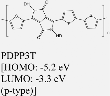
MoS2 | VD & Type-I | Enhanced | Kwon et al., Adv. Sci. 2022,30 |
| Fluorinated fullerene (C60F48) (p-type) | WSe2 | VD | — | Z. Song et al., 201750,156 |
| ATTO 725 (p-type) | (1L/2L) WS2 | Spin-coated | Eenhanced | Morales et al., 2023,29 |
| Type-I | ||||
| Type-II | Quenched | |||
4. Strong optical response in TMDO
4.1. Novel phenomena in TMDO hybrid heterostructures
The commonly accepted mode of formation of the interlayer exciton is through the intralayer transfer process. Even though TMD layers in a TMD heterostructure often show moiré patterns because of the relative rotation between layers with similar lattice constants, layers in a TMDO heterostructure usually have lattice constants that are vastly different. For instance, the lattice constants of PTCDA (a = 3.78 Å, b = 19.30 Å, and c = 10.77 Å) are larger in comparison to the lattice constants of MoS2 (a = b = 3.19 Å, and c = 17.65 Å).14 Importantly, it has also been reported that due to their static dipole moment, the ILX emission energy is tunable by means of out-of-plane electric field,161,162 thus, establishing a signature of ILX emission that distinguishes it from other intralayer or defect-related states.157 The optical properties of the TMDO hetero interface are predominantly influenced by the coulombic bound state of an electron and a hole, which are confined within separate layers. This emergence of complex and fascinating excitonic systems is due to the interplay between the geometrical arrangement, layer charge-polarization, and valley physics intrinsic to monolayer TMDs.14
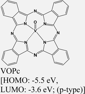
In a recent study, Y. Kong and collaborators have made an important observation of a new PL emission peak occurring at a near-infrared wavelength of approximately 805 nm. This emission peak is attributed to the presence of interlayer charge transfer excitons, so-called interlayer excitons in type-II VOPc/MoS2 (p–n junction) TMDO heterostructures (Fig. 6a), which is crucially dependent on the interface mid-gap states.13 A new room temperature–stable ILX formation mode via direct interlayer photo excitation in TMDO is discussed for the first time. This ILX emission in MoS2/VOPc is further confirmed by the Hersam group.163 They employed femtosecond transient absorption measurements (TA) to explore the mechanism of photoinduced charge transfer and the generation of interlayer excitons in MoS2/VOPc-based type-II heterojunctions. Upon excitation of 514 nm laser light at the VOPc/MoS2 heterojunction, electrons in both VOPc and MoS2 undergo simultaneous transitions to their respective conduction bands. VOPc is an extremely narrow bandgap p-type semiconductor,164 while MoS2 is an n-type semiconductor.165Fig. 6a shows the comparison of the individual emission peak at ∼665 nm and 880 nm of VOPc. The band energy level of the CBM of MoS2 is located below the LUMO level of VOPc (Fig. 6c). Thus, the electrons transfer from the LUMO level of VOPc to the CBM level of MoS2 to reduce their energy and accumulate there in large numbers, effectively reducing the PL of MoS2 in the heterostructure. Moreover, the analysis of the density of states (DOS) reveals the presence of multiple mid-gap states, distinct from defect-related states. These mid-gap states are observed far from the Fermi level, yet they appear near the LUMO level of VOPc and are in proximity to the CBM of MoS2, as depicted in Fig. 6c. The pre-occupied, photo-induced charge carriers can relax to these metastable, empty mid-gap states. In addition, the inrush electron could also transfer from the CBM of MoS2 to the mid-gap states because their energy levels are energetically very close to each other. As a result, net electrons accumulate near the valence band maxima of MoS2 in the heterostructure, as do net holes in the interface mid-gap states of VOPc. They form an interlayer electron–hole pair, i.e., ILX. As a result, a new sharp-transition (emission) peak with an energy of ∼1.54 eV (805 nm) in the NIR region appears.13 This type of observation is reported for the first time in TMDO.
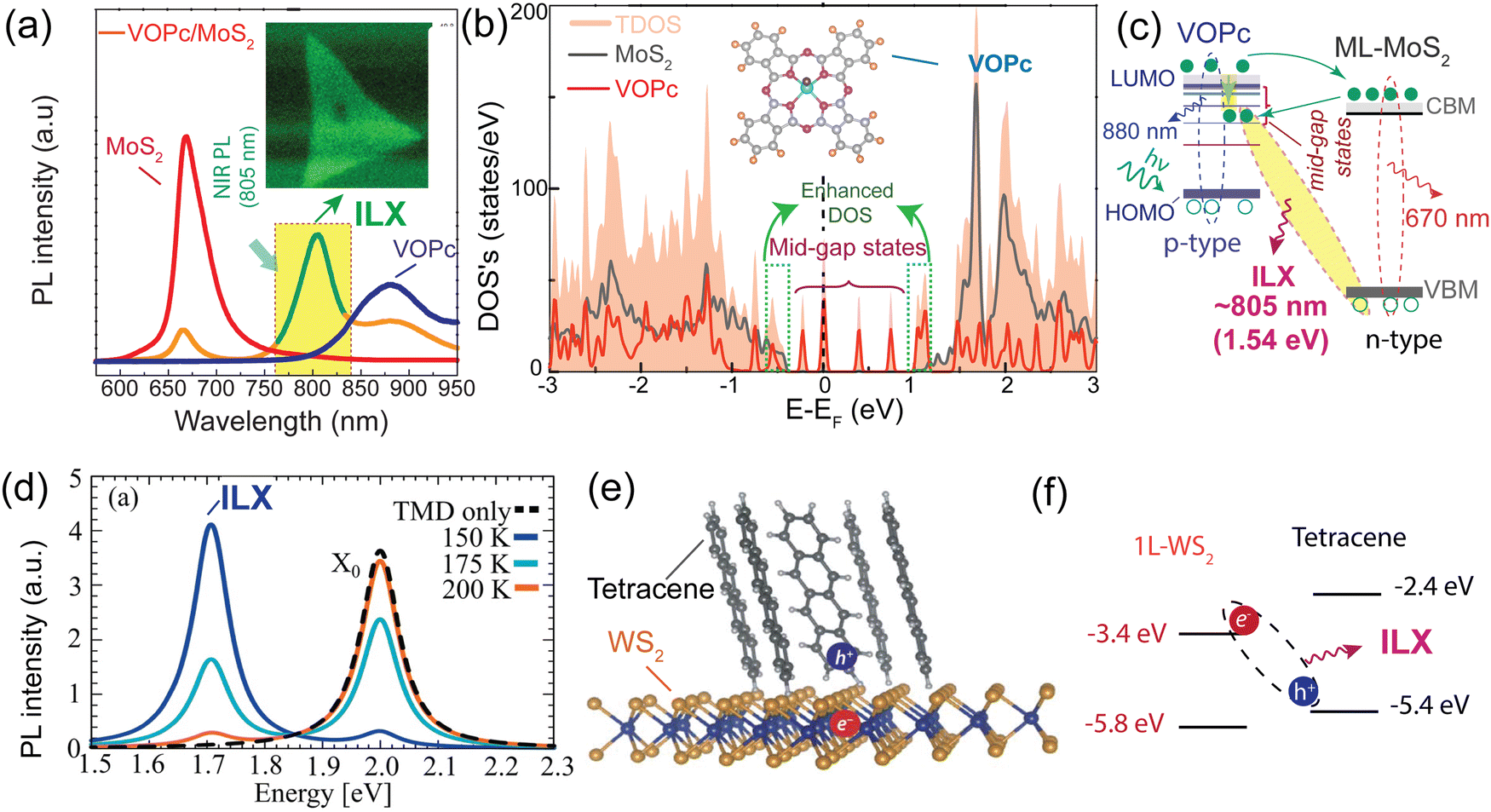 | ||
| Fig. 6 (a) PL emission spectra of the VOPc/MoS2 heterostructure system. A striking feature is a NIR PL appearing around 805 nm (∼1.54 eV) shown in the yellow-shaded box and inset PL mapping. (b) Total density of state (TDOS) of VOPc/MoS2 heterostructures. (c) Schematic representation of the energy band alignment of VOPc/MoS2 (shaded area indicates the possible ILX formation). (d) PL spectra of 1L-WS2, Tc thin film, and a 1L-WS2/Tc. The new emission band at 1.7 eV signifies the formation of ILX. (e) Schematic of the formation of CT excitons and (f) type-II electronic band alignment of the 1L-WS2/Tc heterostructure. (a)–(c) Reproduced from ref. 13 with permission from Royal Society of Chemistry, copyright 2022 and (d) reproduced from ref. 19 with permission from Royal Society of Chemistry, copyright 2023. (e) and (f) Reproduced from ref. 18 with permission from AAAS, copyright 2018. | ||
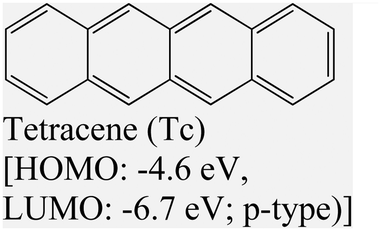
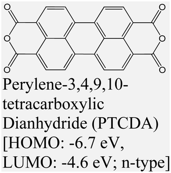
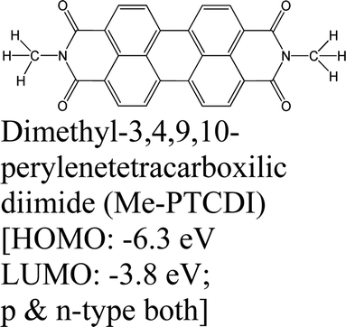
In molecular physics, charge-transfer (CT) excitons emerge as a result of an electron and a hole occupying neighboring molecules. These excitons are most commonly observed in organic and molecular crystals, where they exhibit a static electric dipole moment.166 The lifetime of a charge transfer exciton at the TMDO heterointerface has been found to be extremely short131,167,168 However, due to the insufficient screening of the interfacial coulombic potential, the spatially separated electron–hole pairs do not exhibit as free quasi particles but rather form bound states with energies in the range of hundreds of MeV.10 This phenomenon gives rise to the formation of charge-transfer (CT) excitons, which exhibit similarities to interlayer excitons. The exact nature of the CT states that emerge at the interfaces of TMDO materials in TMD incorporated-molecular semiconductors remains unresolved. In recent research, detailed investigations were conducted to study the formation and transport of charge-transfer (CT) excitons in a type-II heterojunction involving 1L-WS2 and tetracene (Tc) molecules.18 The PL spectrum shows a notable resonance at 2 eV, primarily from the bright intralayer KK exciton at higher temperatures (>200 K), as depicted in Fig. 6(d). Upon decreasing the temperature, a secondary peak at approximately 1.71 eV becomes evident, aligning with the anticipated position of the intralayer exciton (ILX).19 At lower temperatures, there is a greater occupancy of the energetically lower ILX states, resulting in a more pronounced ILX resonance within the PL spectra. Consequently, the temperature serves as an externally adjustable parameter for tuning the relative visibility of ILXs. The CBM of the 1L-WS2 is at −3.4 eV, which is lower than the lowest unoccupied molecular orbital (LUMO) level of Tc molecules at −2.4 eV. This energy arrangement facilitates electron transfer from tetracene (Tc) to WS2. However, the VBM of WS2 is located at −5.8 eV, which is lower than the highest occupied molecular orbital (HOMO) level of Tc at −5.4 eV, enabling hole transfer from WS2 to Tc. (Fig. 6f). The emission band detected at 1.7 eV is attributed to the presence of interlayer charge-transfer (CT) excitons. Further explanation is given that the quasi-flatness of the molecular dispersion means that ILXs are spread over a larger area of momentum space, reflecting its real space localisation. Furthermore, since the Brillouin zones of WS2 and Tc layers are considerably different, they assume that all ILXs are bright as no momentum transfer is required. In this TMD/organic heterostructure, electrons are localized on the 1L-WS2 layer, while holes are localized (or could carriers be almost immobile with heavy effective mass) on the Tc film.19,169 The distinct energy band alignment between the two materials gives rise to the formation of these interlayer CT excitons. The investigation reveals further that the photoexcitation energy below the Tc bandgap at 2.1 eV exclusively excites WS2 while suppressing the background emission from Tc at an energy similar to those of the CT excitons. The broad emission observed from the interlayer CT excitons indicates a distribution in the CT exciton energy levels. The charge-transfer (CT) excitons demonstrate significantly longer photoluminescence (PL) lifetimes compared to the singlet exciton of Tc (∼100 ps) or the A exciton of WS2 (∼500 ps) (Fig. 6d). To further confirm this, photoluminescence excitation measurements were conducted, verifying that the excitation of the A exciton in WS2 results in CT exciton emission.18 These findings present a promising pathway for manipulating the optoelectronic characteristics of van der Waals heterojunctions comprising 2D TMD materials and organic semiconductors. Further harnessing the structural deformability inherent in a two-dimensional molecular crystal is a way to introduce a periodic nanoscale potential, which has the capability to confine ILXs.141 The periodic modulation of molecular orbital energies serves as highly efficient trapping sites for IXs. Notably, when ILXs are generated within the PTCDI/MoS2 system, a swift spatial concentration of electrons within the organic layer near the interface can be observed, underscoring the remarkable efficacy of these interfacial ILX trapping mechanisms.
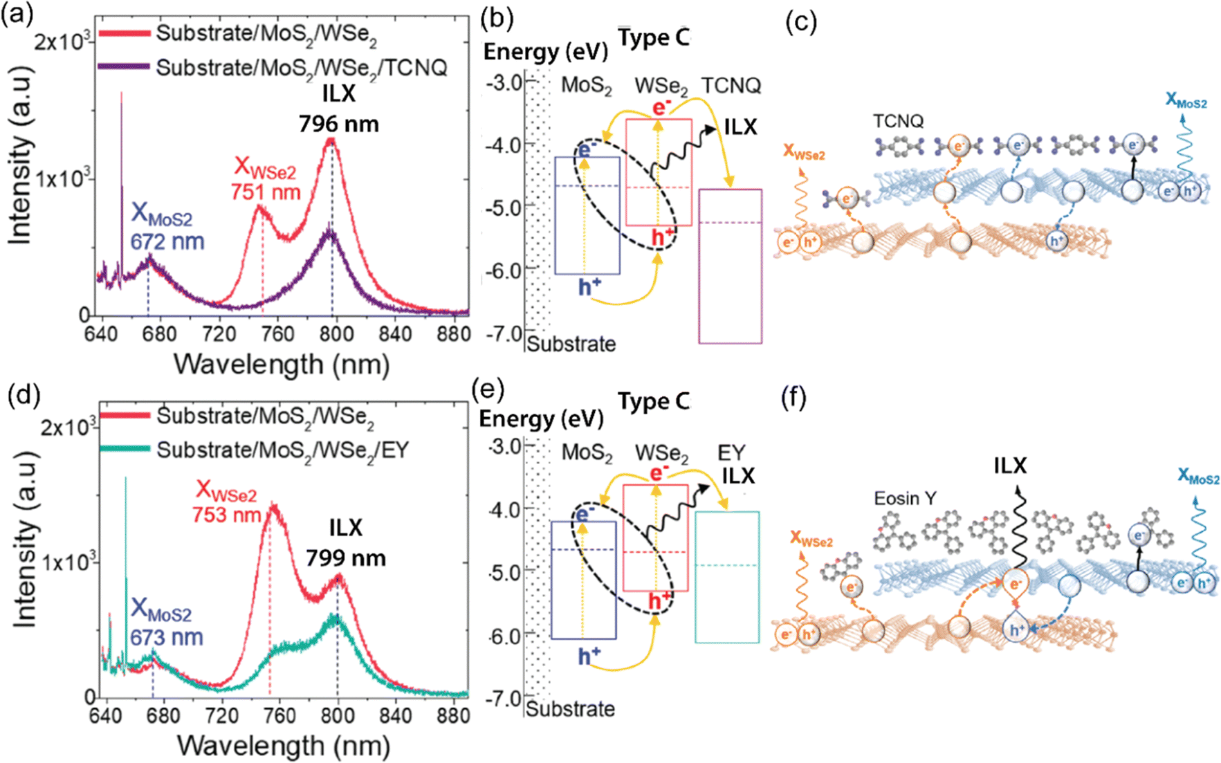 | ||
| Fig. 7 (a) PL spectra of MoS2/WSe2 (red) and MoS2/WSe2/TCNQ (purple). Peak positions of MoS2 exciton (blue), WSe2 exciton (red), and ILX (black) of MoS2/WSe2 are marked with vertical dotted lines. While XWSe2 emission is quenched completely, interlayer excitons are reduced moderately by the TCNQ layer. (b) Energy level diagram of MoS2/WSe2/TCNQ, which forms a discontinuous type-I/type-II alignment (Type-C). (c) WSe2/MoS2/TCNQ heterointerface, photoinduced electron transfer from MoS2 to TCNQ (dotted line) resulting in the quenching of ILXs PL emission. Doping-induced charge transfer may also occur, as illustrated by the black solid line. (d) PL spectra of MoS2/WSe2 (red) and WSe2/MoS2/EY (green). ILX PL emission is decreased slightly with the EY layer. (e) Band energy alignment diagram. (f) WSe2/MoS2/EY hybrid structure; photoinduced charge transfer to EY is suppressed, and interlayer excitons generate a strong PL signature even with p-doping (solid line). (a)–(f) Reproduced from ref. 170 with permission from American Chemical Society, copyright 2020. | ||
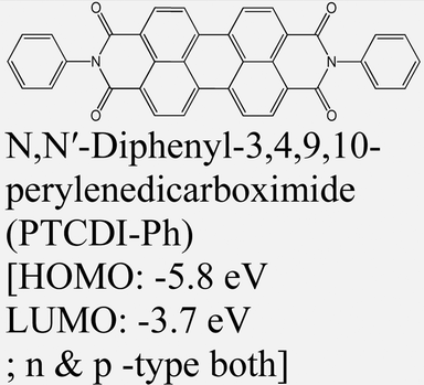
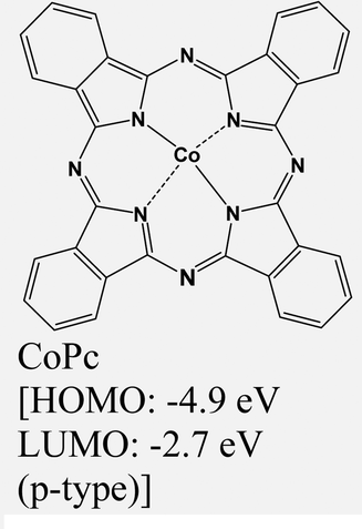
Hybrid TMDO heterostructures comprising MoS2/B3PyPB/WSe2 or MoS2/EY/WSe2 demonstrate distinct and unique optoelectronic properties in comparison to MoS2/WSe2. The nature of the organic molecules significantly influences these optoelectronic characteristics.175 Additionally, investigations have revealed that the introduction of large energy gap organic molecules such as 1,3-bis(3,5-dipyridin-3-ylphenyl)-benzene or B3PyPB reduce the dielectric constant heterostructures. The organic layer also increases the distance between electron and hole charges in ILX. Consequently, the incorporation of organic layers results in a notable blueshift in the interlayer exciton (ILX) emission. Apart from the dielectric screening, the band alignment with the organic layer plays a significant role in altering the interlayer emission substantially. The inclusion of EY creates an energy state situated between MoS2 and WSe2, inducing a transition from tunneling to band-assisted transport. Consequently, the ILX emission experiences an even higher-energy blue shift. Additionally, the use of electron- or hole trapping layers, such as TCNQ or CoPc, respectively, can lead to the complete suppression of the interlayer emission.175 Therefore, chemical modification of TMDs provides a versatile and effective approach toward reconfigurable, high-performance optoelectronic and excitonic devices using 2D heterostructured TMDs with modulated properties. These results provide critical insights into interlayer excitons at the TMD/TMD heterointerfaces and open up an adaptable approach for selectively tailoring them for optoelectronic applications. With the vast library of organic dyes, this approach could become a powerful platform to understand and regulate excitons in 2D materials. For example, photochromic molecules such as di-arylethenes can be used to switch the energy levels in response to external photoirradiation.59 Thus, both interlayer and intralayer exciton behaviors could be controlled dynamically and remotely.
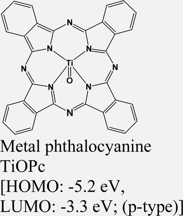
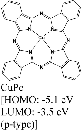
 . Here, Δρ(x, y, z) represents the charge density difference of the adsorption complex concerning the noninteracting individual units, i.e., Δρ(x, y, z) = ρOrg/TMD − ρOrg − ρTMD.176,177 In experimental investigations, photoelectron spectroscopy techniques (including photoemission and inverse photoemission) and scanning tunneling spectroscopy are employed to ascertain the energy positions of the frontier states and core levels within the organic and TMD layers. By analyzing the shifts in core or frontier levels in the energy diagram, one can calculate the alterations in the local electrostatic potential and probe the valuable insights into the type of doping and the degree of charge transfer occurring in the system. To comprehend the impact of adsorbing organic layers on the electronic and interfacial characteristics of TMDs, the plane-averaged charge density difference (CDD) is analyzed for the TMDO heterostructures.176 To quantitatively analyze the charge transfer, the line density of the CDD along the z-axis (normal to the TMD surface), denoted as Δρ(z) is typically studied. In recent theoretical calculations involving 2D-TMD (MoS2, MoSe2, WS2, WSe2) and organic (Pentacene, PTCDA) heterostructures, diverse amounts of transferred charge have been observed, ranging from 0.0018 × 10⁻³e to 0.0109 × 10⁻³e. To quantify the charge transfer, one can typically study the line density of CDD along the z-axis (normal to the surface of TMD) (Δρ(z)). In recent theoretical calculations involving 2D-TMD (MoS2, MoSe2, WS2, and WSe2) and organic (Pentacene, PTCDA) heterostructures, diverse amounts of transferred charges have been observed, ranging from 0.0018 × 10⁻³e to 0.0109 × 10⁻³e.176 Again, the charge transfer analysis reported that there is a net amount of 0.059 electrons per CuPc molecule and 0.052 electrons per TiOPc molecule transferred to the respective monovacancy in MoS2 surfaces.104 Further, density functional theory (DFT) studies reveal that pentacene adsorbed on 1T-type monolayer MoS2 has a large degree of charge transfer ranging from 0.44 to 0.87 e per molecule, which, in turn, changes the Fermi energy level of MoS2 by up to 1 eV.132,178 The degree of charge transfer per molecule relies on the precise molecular adsorption geometry and the diverse phases of the substrate.132 Furthermore, the hybridization of 2D MoSe2 with pentacene in type-I band alignments enables efficient and layer-dependent exciton pumping across the TMDO interfaces. Interestingly, the efficiency of interfacial exciton pumping surpasses that of the photoexcitation process in MoSe2/pentacene by more than 86 times, despite the pentacene layer exhibiting much lower optical absorption compared to MoSe2.16Fig. 8c depicts the electronic band alignment between pentacene and MoSe2,93,179 where the MoSe2/pentacene forms a type-I heterojunction. In particular, the HOMO of pentacene lies below the VBM of 1L MoSe2 and the LUMO of pentacene resides above the CBM of 1L MoSe2. As illustrated in Fig. 7c, when carriers are photoexcited, they transfer from pentacene to MoSe2 due to the significant built-in potential and subsequently recombine radiatively. This process leads to an increase in the PL intensity in the MoSe2 layer and a reduction in the PL intensity in the pentacene layer, as shown in Fig. 8a. This substantial enhancement in pumping efficiency can be attributed to the elevated quantum yield in pentacene and the ultrafast energy transfer occurring within the TMDO interface. Additionally, the precise dielectric environment engineering provided by the organic counterparts significantly alters the binding of charged excitons in monolayer MoSe2. Further, a strong PL enhancement and quenching behaviors were also reported in the PDI/MoS2 heterostructures (here, PDI refers to perylene derivatives PTCDA or PTCDI-Ph) (Fig. 8d).14 There are several key reasons provided for this enhancement of the PL signal in the PTCDA/MoS2 heterostructure: first, an increased carrier transition probability because of the enhancement of the DOS (due to significant hybridization of C-pz and Mo-dz2 orbitals). Second, the PTCDA/MoS2 heterostructure exhibits an increased exciton/trion ratio, and it effectively suppresses nonradiative emission.14,139 Further, resonance energy transfer (RET) from a red-emitting WS2 monolayer (1L-WS2) to a layer of near-infrared (NIR)emitting organic dye molecule-based type I heterostructures is demonstrated.29 It is found that the total PL yield of the heterostructures is up to a factor of eight higher than the PL yield of pristine 1L-WS2. They have explained that the efficient RET alone is necessary but not sufficient for the desired PL enhancement. Additionally, a key requirement is maintaining the high PL yield of the dye when in direct contact with 1L-WS2. This necessitates a type-I energy level alignment at the heterointerface. Photoelectron yield spectroscopy confirms this alignment. Although some level positions are uncertain, it is clear that the energy level alignment does not drive exciton dissociation or charge transfer between the dye and 1L-WS2, thereby preserving a high PL yield in the hybrid structure. Again, a strong decrease in the PL of the dye is observed on 2L-WS2 when it gives type II heterostructures. The significant PL quenching can be elucidated through the energy level alignment occurring at the interfaces of the 2L-WS2/Atto hybrid system. The VBM of 2L-WS2 shifts upward, creating a type-II alignment with the dye's HOMO at ≈5.4 eV. This alignment allows hole transfer from the dye's HOMO to the TMD's valence band, leading to exciton dissociation and reduced PL yield. S Park et al. recently reported on PTCDA/MoS2 type-I heterostructures with enhanced PL emission.20 Initial expectations pointed towards a staggered type-II energy level alignment and excited state interfacial charge transfer. However, through inverse and direct angle resolved photoelectron spectroscopy, they discovered a straddling type-I level alignment between PTCDA and ML-MoS2 on insulating sapphire. PTCDA exhibited a wider energy gap. Further analysis through PL and sub-picosecond transient absorption revealed sub-picosecond resonance energy transfer, involving electron–hole pair (exciton) transfer from PTCDA to ML-MoS2. This transfer significantly enhanced the PL yield from ML-MoS2 in the heterostructure, consequently modulating the overall photoresponse. Again, the PL emission spectra of the DY1/MoS2 heterostructure showed quenching of the DY1 emission but enhancement of the MoS2 emission, indicating a strong electronic interaction between these two materials. The MoS2 flakes coated with DY1 via evaporation displayed a 1.7-fold increase in PL emission compared to the untreated MoS2 flakes. Minimal changes in the light-induced contact potential difference (CPD) at the DY1/MoS2 interface eliminated the possibility of an interlayer charge transfer process, confirming the formation of a type-I heterojunction.30 Again, it is found that while the excited-state electron transfer rate from TMDs (MoS2 and WSe2) to fullerenes (C60) is relatively insensitive due to the band offset (more details discussed earlier), the electron transfer (ET) rate from TMDs to PTCDA is reduced by an order of magnitude when the band offset is quite large.140 For the perylene crystal, the sensitivity of the electron transfer rate on the band offset is elucidated by the 1D nature of the electronic wave function, which limits the availability of states with the appropriate energy to accept the electron.140 Recent research has demonstrated that using organic superacids like TFSI for MoS2 surface passivation significantly reduces defect-induced nonradiative recombination, resulting in a near-unity PL efficiency.180 Moreover, employing a p-doping procedure, HBr efficiently suppresses trap-state emissions and amplifies the emission of neutral excitons and trions in defective monolayers of MoSe2. This results in a remarkable 30-fold increase in the overall PL intensity at room temperature.181 These defective states can also align with the orbital states of functionalized molecules, influencing carrier properties in TMD materials. Most recently, Liu's group has recently introduced a novel method involving pre-melting and re-solidification of chalcogen powders (S and Se). This technique ensures a consistent supply of chalcogens, facilitating the high quality and uniform growth of monolayer TMDs. After annealing the chalcogen powder in an inert environment, the precursor's surface area decreases significantly, which is beneficial for the subsequent growth of 2D TMDs. This method has been successfully extended to the growth of other high-quality 2D TMDs, including MoS2, WSe2, and MoSe2, demonstrating its versatility and effectiveness.182,183
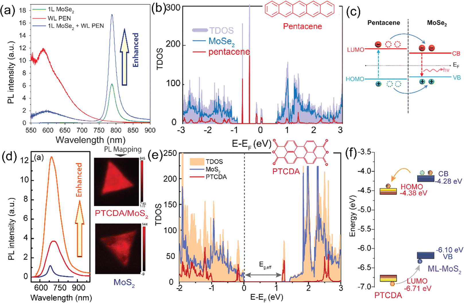 | ||
| Fig. 8 (a) PL emission spectra of 1L MoSe2 and WL-PEN type-I heterostructure. (b) Calculated density of states of the MoSe2/pentacene heterostructure. (c) Type-I band energy alignment of a MoSe2/pentacene heterostructure. (d) PL spectra and PL maps of the PTCDA/MoS2 type-II hybrid structure (orange), PTCDA (red), and MoS2 monolayer (blue). (e) DFT study of PTCDA/MoS2 heterostructures: TDOS and PDOS of the PTCDA/MoS2 heterostructure, PTCDA and MoS2. (f) Type-II band alignment for PTCDA/MoS2 schematically showing the photoexcited carriers’ transfer within the hybrid heterostructure interface. (a) and (c) Reproduced from ref. 16 with permission from Wiley-VCH, copyright 2018. (b) Reproduced from ref. 176 with permission from Wiley-VCH, Copyright 2020. (d)–(f) Reproduced from ref. 14 with permission from Wiley-VCH, copyright 2019. | ||
The Fourier plane images of the emission intensity reveal a horizontal alignment of the excited state dipoles for both MoSe2 and PTCDA. As a result of efficient energy transfer across the interface, the emission intensity of the donor (PTCDA) decreases, while that of the acceptor (MoSe2) increases. Moreover, the energy transfer is accompanied by a shortened fluorescence decay time of the donor, considering a new channel for nonradiative recombination from the donor's perspective. When a 10-nm-thick spacer (Al2O3) was introduced and a new heterostructure of PTCDA/Al2O3/MoSe2 formed, the energy transfer process was blocked; thus, no discernible change in lifetime was observed in the new heterostructure. The exciton lifetime of MoSe2 is considerably shorter than that of PTCDA. However, due to Förster resonance energy transfer (FRET), the excited state of MoSe2 continues to be populated, leading to a prolongation of the effective PL lifetime of MoSe2 in the heterostructure. PL excitation experiments have revealed that the emission intensity of MoSe2 reaches its maximum at the absorption peak of PTCDA in the heterostructure, providing direct evidence of efficient energy transfer from PTCDA to MoSe2.128
Finally, recently, the energy transfer on a prototypical heterostructure consisting of tetracene (Tc) and a monolayer WSe2 was studied using ultrafast spectroscopy.137 Upon photoexcitation in type-II WSe2/Tc heterostructure, an ultrafast (∼3.4 ps) singlet exciton energy transfer from tetracene to WSe2 occurs, followed by a 16.5 ps hole transfer from WSe2 to tetracene, resulting in long-lived (∼565 ps) charge separation. Notably, this charge separation takes place prior to the slow singlet fission (SF) process (>20 ps) in tetracene. However, this study presents various challenges and emphasizes the need for deliberate design to enhance singlet fission in 2D optoelectronic devices.
4.2. Doping
It is well known that defective states in TMDs, which are formed within the bandgap near to the VBM or near to the CBM, can play a significant role for carrier mobilities and quasiparticles such as excitons and trions.186–188 Furthermore, these types of states are often associated with dangling bonds, which may serve as active sites for the chemical or physical adsorption of different species.189–192 In particular, the interplay between the localized defective states and organic molecular orbitals may result in new optical excitations and modulation of electron–hole recombination processes.193–195 A recent study has showed that the passivation of the MoS2 surface with organic superacids greatly suppressed the defect-mediated nonradiative recombination and led to near-unity photoluminescence.180 In addition, resonance of these defective states with the orbital states of functionalized molecules or atoms was found to enable the rectification of carrier content and polarity in the host TMD materials. However, the combined impact of doping molecules and sulfur vacancies on the charge transfer and electronic properties of monolayer MoS2 remains largely unexplored. The interactions between molecules and semiconducting 2D materials have been studied before. For example, the control of charge carriers and PL emission by hybrid 2D-TMDs sheets such as MoS239,40 and WS266,196 with chemical functional groups was investigated. Many prototype devices, demonstrating the robust molecule-MoS2 interaction, were engineered to realize highly effective gas sensors and detectors. Physisorbed or chemisorbed molecular groups were shown to lead to efficient layer-by-layer exfoliation and significant modification of the surface properties of MoS2 layers.197 In addition, because of the atomically thin nature, the accumulated or depleted charges transferred between the molecules and MoS2 were demonstrated to result in a remarkably high sheet charge density.21,197 Therefore, a proper chemical functionalization treatment of TMDs by an organic layer results in modulated photoluminescence198–201 and enhanced TMDO constituent stability.181 The most commonly used molecular non-covalent p-dopants are tetracyanoquinodimethane (TCNQ) and tetracyanoethylene (TCNE).202,203 These materials are strong electron acceptors with a solid-state electron affinity of 5.2 eV, and the planarity of 2,3,5,6-tetrafluoro-7,7,8,8-tetracyanoquinodimethane (F4TCNQ) enables efficient blending with many hosts.Moreover, doping is attained by exposing the crucial TMD surface to solutions containing a pentamethylrhodocene dimer as the reductant n-dopant and “Magic Blue” [N(C6H4-p-Br)3]SbCl6 as the oxidant (p-dopant).204 The current–voltage characteristics of FETs reveal that irrespective of their initial transport behavior all key TMDs can serve as p- or n-channel devices upon appropriate doping. In Fig. 9a, the arrangement of dopant molecules at TMDO interfaces under low coverage conditions is shown, where the molecules lie flat on the surface. Various donor and acceptor molecules are depicted, and their respective energy levels (HOMO/LUMO) are indicated with respect to MoS2 (Fig. 3). The optoelectronic properties of 2D TMDs (MoS2, MoSe2, and WSe2) were modulated by incorporating two metal-centered phthalocyanine (MPc) molecules, namely NiPc and MgPc.106 The investigation further demonstrates the selective and reversible engineering of PL emission by facilitating energetically favorable electron transfer from photoexcited TMDs to MPcs.
 | ||
| Fig. 9 (a) Band alignment of MoS2, MoSe2, WS2, and WSe2 along with effective ionization energy (IE) of the n-dopant and electron affinity (EA) of the p-dopant. (b) and (c) PL emission of MoS2 after n- and p-doping treatment. (d) Band alignment of MoS2, MoSe2, and WSe2 along with reduction potentials of NiPc and MgPc and (e), (f) corresponding PL spectra. (g) Schematic of functionalization scheme 2H to 1T phases. (h) HRTEM image of an atomically thin-phase boundary (indicated by the arrows) between the 1T and 2H phases in 1L MoS2. (i) PL spectra obtained from 1L MoS2 (2H phase), from the metallic 1T phase and from the functionalized 1T phase. A strong PL peak at ∼1.8 eV is observed for the 2H phase, consistent with single-layer 2H MoS2, whereas PL is quenched after conversion to the metallic 1T phase. Inset: A typical CVD-grown flake of 1L MoS2. (j) Modulation of photoluminescence peak intensity with the increasing amount of functionalization. (b) and (c) Reproduced from ref. 204 with permission from Wiley-VCH, copyright 2018. (d)–(f) Reproduced from ref. 106 with permission from American Chemical Society, Copyright 2015. (g), (i) and (j) Reproduced from ref. 199 with permission from Springer Nature, Copyright 2014. (h) Reproduced from ref. 276 with permission from Nature Publishing Group, copyright 2014. | ||
4.3. Defect repairing
In general, commercially available 2D-TMDs may contain defects in their lattice structure, including atom vacancies within the basal and/or edge planes, as well as substitutional defects. Specifically, the presence of chalcogenides (S, Se, and Te) in TMDs contributes to their low sublimation temperature (<200 °C), resulting in their volatility and the occurrence of defects. These chalcogen vacancies create energy band levels within the gap states, which function as charge scatterers and traps. As a result, this phenomenon leads to the quenching of PL, decreased mobility, and enhanced hysteresis properties in TMDs.186,205,206 Significantly, TMDs obtained through mechanical exfoliation generally exhibit a lower density of inherent defects than the sheets produced via chemical vapor deposition (CVD), chemical, or liquid-phase exfoliation methods. The presence of a high density of defects in the latter limits their optoelectronic applications.89 To address this, the concept of ‘defect healing’ or ‘repairing’ becomes crucial in order to enhance the electronic performance of TMDs, making them suitable for large-area fabrication and practical industrial applications. In 2D-TMDs, the surface is often considered inert and challenging to functionalize covalently due to dangling-bond free surface. However, chalcogen (S, Se, and Te) vacancy sites possess reactive dangling bonds that can serve as anchoring sites for specific molecular species.6,207 As a result, a promising defect repairing strategy involves exploring molecular functionalization at these defect sites. This approach offers potential for enhancing the optical and electronic properties of defective 2D-TMDs.As an example of a defect healing approach, thiol (-SH) molecules were applied to functionalize sulfur vacancies in TMDs, supported on substrates or in solutions. In this functionalization process, the sulfur S atom in the thiol group (-SH) forms a covalent bond with a sulfur vacancy site, effectively repairing the defect while simultaneously functionalizing the TMD. In another research work, Nguyen et al. employed thiol (R–S–H) chemistry to functionalize the surface of MoS2, which resulted in the passivation of defects, hence modulating the electronic properties.208 The functionalization of MoS2 with thiols induced alterations in its chemical properties, offering potential applications in the design of efficient sensors and catalysts. Two categories of thiols were investigated: (i) thiols with aromatic rings possessing distinct electron-withdrawing capabilities, such as p-mercaptophenol and thiophenol and (ii) alkyl thiols with varying chain lengths, including 1-propanethiol, 1-nonanethiol, and 1-dodecanethiol.209 Thiol functionalization has demonstrated the capability to enhance the electronic properties of MoS2 devices by repairing intrinsic defects or controlled vacancies introduced via ion irradiation. Additionally, annealing processes were found to cleave the S–C bonds, releasing the thiol-grafted molecule and restoring the integrity of the MoS2 lattice. The incorporation of thiol-based dopant groups not only facilitated defect healing but also introduced simultaneous doping effects. Thus, grafting the functional groups may result in the passivation of defects and reduction of the charge scattering sites. Thiol functionalization strategies have recently demonstrated that they effectively advance the optoelectronic performance of TMDs such as WSe2.210 This effective approach has proven successful not only for transition metal disulfides but also for TMDs with Se and Te terminations.
Defects in TMDs fall into two main categories: chalcogen vacancies and transition metal vacancies. Chalcogen vacancies, where chalcogen atoms (typically S/Se/Te) are missing from the crystal lattice, are more common. These defects can be unintentionally generated by adjusting growth parameters such as temperature, gas flow, precursor ratios, and substrate. Temperature variations and thermal annealing can also induce structural changes in chalcogen atomic defects within 2D TMDs. Understanding this evolution is crucial to prevent surface/interface degradation and holds significance for future device applications. For instance, annealing monolayer MoTe2 at moderate temperatures leads to the formation of Te vacancies and pinholes, with their extent increasing as the temperature rises. Further, in TMDs, chalcogen vacancies (S, Se, and Te) can be effectively filled with isoelectronic oxygen atoms and chloride ions.68,211,212 Specifically, laser irradiation in air has been reported to greatly enhance the optoelectronic properties of defective WSe2. This process facilitates the binding of oxygen atoms at Se vacancies.212 For instance, laser irradiation can generate Te vacancies in MoTe2, leading to a phase transformation from 2H to 1T.213 Additionally, plasma treatment, whether with oxygen plasma or argon plasma, proves effective in creating chalcogen atomic defects in 2D TMDs.214 Tailoring chalcogen atomic defects to manipulate properties and enhance device performance can be achieved by adjusting synthesis parameters to introduce stoichiometry deviations during crystal growth and by applying post-growth treatments to selectively create these defects. For instance, Pranjal Kumar Gogoi demonstrated oxygen passivation in MoS2, altering exciton and trionic properties.215 It is also highlighted that the possibility of substitutional oxygen atoms is more prevalent in the crystal structure of TMDs. Therefore, nanoscale characterization techniques were utilized to investigate the defect origins in MoSe2 and WS2. These oxygen substitutional atoms can serve as anchoring sites for further functionalization, similar to what has been previously discussed for SAMs on the top surface of TMDs.64
The defect healing approach for chalcogens other than sulfur (S), such as selenium (Se) and tellurium (Te), is indeed a valuable aspect of this research field. An air-stable p-doping of WSe2 has been successfully demonstrated through the chemisorption of NO2 at 150 °C. This innovative process led to a remarkable reduction in contact resistance with the Pd metal by five orders of magnitude, resulting in a degenerate doping concentration of 1.6 × 1019 cm−3. Their work provides a promising pathway for achieving air-stable p-doping in WSe2, with broad potential applications.68 In an exciting development, researchers reported the creation of an optically switchable multilevel FET by interfacing WSe2 with a bicomponent donor–acceptor-acceptor (DAE) blend. This blend consisted of two DAE molecules with specific energy levels engineered to trap either electrons or holes in WSe2. The resulting device demonstrated the ability to modulate both electron and hole transport simultaneously through remote light stimuli. This approach holds promise for the development of optically switchable ambipolar FETs and is applicable to various 2D materials.216 Moreover, a novel method has been introduced to rectify Te vacancies within defective MoTe2 by filling them with reactive oxygen via a low-pressure annealing process. This technique resulted in significant improvements in FET characteristics, including greatly enhanced current density control and a record-high hole mobility of 77 cm2 V−1 s−1.217 A one-step synthesis method was reported for producing atomically homogeneous Fe-doped VSe2. This material exhibited enhanced catalytic activity, particularly in the hydrogen evolution reaction, making it promising for various catalytic applications.218 Defect-induced magnetism was observed in single-layer PdSe2, primarily attributed to Se vacancies that create in-gap defect states. This discovery transforms PdSe2 into a 2D magnet and highlights the common occurrence of defects, especially Se vacancies, during exfoliation. The findings position PdSe2 as an ideal platform for the study of defect-induced phenomena and offer insights for experimental control of defect patterns.219
4.4. Phase engineering with covalent functionalization
Chemical modifications such as increasing their solubility in common solvents offer additional opportunities to modulate the properties of 2D TMDs. Although theoretical studies on the functionalization of TMDO have shown promising progress, the experimental covalent functionalization still poses challenges.199,209,220–223 In past, functionalization has been generally achieved via reductive alkylation by introducing a halide reagent to n-doped carbon nanotubes and graphene.224–226 In recent studies, a novel approach to functionalize 2D TMDs involves ligands interacting with unsaturated metal atoms located at the edges or defects on the basal plane. This method opens up a promising avenue for enhancing the properties of these materials.199 Further, the chemical exfoliation can result in defective sheets, and hence, some of the functionalizing molecules may also bind to defect sites. The organohalide solution-functionalization reactions of the chemically exfoliated 2D monolayer were highly efficient because of the functional group of TMD (e.g., MoS2, WS2, and MoSe2). However, the functionalization reactions are usually considered efficient if the ratio of the functional group per 2D TMD surface area is greater than 25%, which is confirmed from the XPS study.209 In a recent study, covalent functionalization of the basal plane of TMDs has attracted significant attention. As discussed in the preceding section, the strategies employed for defect functionalization also led to the establishment of covalent bonds. This versatility opens up new possibilities for tailoring the properties of TMDs via covalent modifications. In this regard, there are diverse approaches that facilitate covalent bonding without necessarily requiring the presence of defects.The key distinction between the two approaches lies in their impact on binding molecules to the surface. In the defect healing process, the number of molecules that can bind is limited by the presence of defects. Conversely, in the direct covalent grafting scheme to the TMDs’ basal plane, a larger quantity of molecules can be immobilized. It is further noted that due to the strong inertness of TMDs, aggressive chemical reactions were required to achieve significant covalent functionalization. The covalent functionalization of semiconducting TMDs has primarily been observed in chemically exfoliated compounds obtained through Li intercalation in solutions. This process results in electron transfer from Li atoms, leading to negatively charged mono- and few-layered TMD flakes. A versatile, general and simple method has been successfully employed for the covalent functionalization of 2D TMD nanosheets, including MoS2, WS2, and MoSe2, without the need for defect engineering. Instead, the functionalization reaction involves electron transfer between the electron-rich metallic 1T phase and an organohalide reactant, leading to the covalent attachment of functional groups (such as 2-iodoacetamide or iodomethane) to the chalcogen atoms of the TMD, as illustrated in Fig. 9g and h.199 The covalent attachment of functional groups to the TMD nanosheets results in significant alterations in their optoelectronic properties. Notably, the metallic 1T phase is transformed into a semiconducting state, leading to pronounced and tunable photoluminescence as well as gate modulation effects in field-effect transistors, as depicted in Fig. 9i and j. Voiry and coworkers reported the formation of C–S bonds on the basal plane of exfoliated MoS2 through a reduction negative charge using an organohalide reactant. The chemically exfoliated sheets, which were initially negatively charged, underwent the reaction leading to the creation of C–S bonds. This process resulted in a functionalization degree of approximately 20%, determined as the ratio of functional groups to MoS2 units.199,227–229 A similar methodology applied to 2D materials, diazonium salt chemistry, was utilized to covalently functionalize the chemically exfoliated TMDs in solutions. Recently, a chemical approach involving aryldiazonium was adopted to achieve surface functionalization of MoS2.230
4.5. Beyond band energy alignment in TMDO: unveiling the influence of molecular orbital interactions, molecular orientation, and thickness variation
When two distinct materials come into contact to form a heterojunction, their electronic states do not remain unchanged or static. Even in 2D vdW interfaces, where the bonding is weak, interactions between orbitals can lead to alterations in the alignment of band energy levels.12 These perturbations involve specific effects on the orbitals, such as hybridization, as well as more general effects related to charge transfer and electrostatic interactions. In this context, hybridization refers to the emergence of new or mixed electronic states in the hybrid TMDO system, where the electron density originates from both the organic molecule and the TMD material. If this hybridization leads to an apparent alteration in the distribution of electron density, it gives rise to ground-state charge transfer, effectively facilitating an electron transfer from one component to the other. Furthermore, the presence of dipoles and charges within molecules can induce changes in the electronic structure of the TMD material, analogous to the effect of a gate voltage in a FET transistor. As a result, the Fermi level of the TMD material may be shifted either upwards or downwards.12 Typically, widely used organic semiconductors including planar phthalocyanine molecules, acenes, and perylene derivatives possess neutral charges and exhibit negligible or small net dipole moments. In such instances, the dynamics of charge carriers is primarily influenced by hybridization and ground-state charge transfer phenomena. As an example, in PTCDA/MoS2 heterojunctions, the process of hybridization combines the S-pz and Mo-dz2 orbitals near the CBM (Conduction Band Minimum) with the conjugated C-pz orbitals (as depicted in Fig. 6b).139 This hybridization process leads to a reduction in the bandgap of MoS2 effectively and an enhancement in the density of states (DOS) near the band edges. This effect further causes a significant increase in the intensity of the PL signal, accompanied by a redshift. Furthermore, a charge transfer phenomenon occurs, which is due to the rearrangement of electron density within the hybrid orbitals. The contrasting optoelectronic behaviors of PTCDA and other non-planar perylene derivatives such as PTCDI-Ph become more apparent when compared. The planar geometry of PTCDA facilitates a higher overlap of molecular π-orbitals with the out-of-plane orbitals in the MoS2 conduction band, leading to more pronounced effects in hybridization and charge transfer. In contrast, PTCDI-Ph's bent structure reduces this overlap, resulting in a less significant impact on the electronic properties of MoS2.14 Consequently, there is a decrease in the net charge transfer between PTCDI-Ph and MoS2, and the surface binding energy obtained from density functional theory (DFT) is 30% lower for PTCDI-Ph as compared to PTCDA.14,139 In another example of the FePc/MoS2 heterostructure, angle-resolved photoelectron spectroscopy (ARPES) has revealed the hybridization between FePc and MoS2 in the vicinity of the K point.231Further, the orientation of organic molecules, film morphology, and thickness are crucial; however, they are often neglected factors in TMDO heterojunctions (see Fig. 10a).12,14,53,232 It is widely acknowledged that interactions between molecules and substrates have a substantial impact on the adsorption of individual molecules onto solid surfaces, playing a pivotal role in directing the orientation of these molecules.233 Recently, Wang et al. have demonstrated the crystallographic structures of diverse 2D atomic crystals via the strategic utilization of an oleamide molecule as a probe, harnessing orientation-dependent interactions with the substrate.234 The process of oleamide assembly onto 2D atomic crystals comprises two simple steps: initially, applying a diluted oleamide solution in chloroform onto the 2D materials via spin-coating, followed by annealing the samples at a moderate temperature. Following this process, dense nanoribbons were observed on various hexagonal 2D atomic crystals, including mechanically exfoliated MoS2, WSe2, ReS2 and other 2D materials (Fig. 10b–d). The strikingly different orientations of oleamide nanoribbons on various 2D atomic crystals, each possessing distinct crystallographic structures, strongly indicate that the alignment of these nanoribbons is probably influenced by the atomic arrangements of the underlying substrates.
 | ||
| Fig. 10 Self-assembly of oleamide on different 2D atomic crystals. (a) Schematic of the oleamide self-assembly on 2D atomic crystals along specific orientations. Hydrogen bonds are indicated with blue dashed lines. (b)–(d) Images of oleamide nanoribbons on MoS2, WSe2 and ReS2 respectively. (a)–(d) Reproduced from ref. 234 with permission from Nature Publishing group, copyright 2017. | ||
These nanoribbons exhibited alignment along three high-symmetry directions with rotations of approximately 120 degrees and covered a substantial area. This investigative approach has led to an intriguing revelation: the periodic atomic arrangement in 2D materials directs oleamide molecules to self-assemble into quasi-one-dimensional nanoribbons, exhibiting distinct alignments that serve as precise indicators of the underlying lattice orientations. Using oleamide molecules as probes, they have achieved the successful identification of crystallographic orientations for approximately 12 distinct 2D materials, all the while preserving their intrinsic properties without degradation.234 As a result, vdW materials offer a distinctive platform for fine-tuning these properties, allowing the growth of high-quality organic phases that may not be observed on other substrates.235 The orientation of a molecule on a surface plays a crucial role in controlling its interactions with the surface. For example, the significance of orientation has been demonstrated in studies involving H2Pc and CuPc films on MoS2. The two phthalocyanine molecules H2Pc and CuPc exhibit different orientations on MoS2. CuPc lies in a π-face-on configuration, whereas H2Pc adopts an approximately edge-on orientation on MoS2.12,51,232,236 The variation in molecular orientation has significantly impacts on the recombination times upon photoexcitation. In the CuPc/MoS2 interface, excitons more readily dissociate, leading to the formation of long-lived free carriers. Several other large π-conjugated molecules such as pentacene and perylenes have been shown face-on orientation to 2D TMD materials.143 The face-on orientation of large π-conjugated molecules such as pentacene and perylenes on 2D TMD materials contrasts with the edge-on orientations observed on conventional surfaces such as SiO2 and sapphire. This orientation/alignment frequently differs from the edge-on orientations observed on more conventional surfaces such as SiO2 and sapphire.232,237 This distinct molecular orientation has led to the emergence of van der Waals materials, particularly hexagonal boron nitride (hBN), as favorable substrates for facilitating the epitaxial growth of functional organic molecules.12
The thickness of 2D TMDs is a crucial factor influencing the band energy level alignment, charge transfer phenomena, and prominence of energy transfer observed at TMDO interfaces.18,131,238 It is demonstrated that the thickness dependence in WS2/Tc heterojunctions results in distinct changes when transitioning from monolayer (1L) to bilayer (2L) WS2. Specifically, with the increase in WS2 thickness, the valence band minimum rises, leading to the blocks of hole transfer to the tetracene layer.18 With the increase in WS2 layer numbers, the interface undergoes a transition from Type-II to Type-I, leading to energy transfer during selective tetracene excitation. In the case of a type-I 1L-WS2/tetracene junction, excitonic energy transfer takes place. To understand this process, dynamics in type I heterostructures constructed with 2L-WS2 and tetracene was examined. In type I heterostructures, the hole transfer from WS2 is inhibited, allowing only excitonic energy transfer.18 The group further observed a correlation between the thickness and the energy transfer speed, with the transfer time increasing from 44 ± 5 ps for 2L-WS2/Tc to 84.8 ± 4.4 ps for 7L-WS2/Tc heterostructures. Even when the energy level alignment remains favorable for charge transfer, variations in the thickness of transition metal dichalcogenides (TMDs) can still impact the photophysics of heterojunctions. The photophysics of heterojunctions can still be influenced by variations in the thickness of TMD, even when the energy level alignment for charge transfer remains favorable. Kafle et al. also addressed the thickness dependence of the TMD layer with phthalocyanine molecules, using MoS2/ZnPc interfaces.53
It is worth to mention that up until now, remarkable progress has been achieved with the study on 2D magnetic TMDs such as CrSe2, CrTe2, FeSe2, FeTe2 and VeTe2,239–242 and novel magnetic properties at the hybrid TMDO interface in the 2D limit remain virtually unexplored for diverse optoelectronic applications. Magnetic molecules, for example, TbPc2 with 2D TMD could give novel properties in the future with diverse applications. In this regard, MOKE techniques could characterize the ultra-thin magnetic layers with thicknesses in the sub-nanometer range.243
5. Advancement in field-effect device applications
5.1. Field-effect transistors (FETs)
Over the last decade, the distinctive electronic, chemical, and physical properties of two-dimensional transition metal dichalcogenides have attracted significant attention. Although in 2D family, pristine graphene has ultrahigh mobility around 104 cm2 V−1 s−1,244–246 zero bandgap and poor switching characteristics, which make it difficult to be used as a channel material. Even though pristine graphene belongs to the 2D family and has extremely high mobility, its zero bandgap and poor switching properties make it challenging to use as a channel material. Therefore, due to their advantageous optoelectronic characteristics and large band gaps of 1–3 eV,247,248 TMDs have gained new research interests, revealing them as a distinct class of materials with distinctive technological potential.247,248 As vdW heterostructures advance technologically from their humble beginnings, more research groups have access to more advanced tools and materials. In particular, the vdW assembly protocols need to be scaled up for any industrial application.249 Consequently, the study of optoelectronic devices incorporating the synergistic properties of TMDs and molecules has emerged as a prominently researched area in present times.In this section, we will further discuss on the device architecture and novel properties of TMDO heterostructure-based FETs (Table 2). This investigation highlights the vast potential of hybrid heterostructures in creating novel devices with distinctive functionalities. In both cases, these devices exploit the semiconducting properties of specific organic molecules, while the TMDO interface plays a pivotal role in determining the device performance. As we will highlight, the controllable manipulation of energy bands at the TMDO heterointerface is beneficial to the devices. This modification is achievable through the application of an electric field controlled by a gate terminal.
| Hetero junction: TMDO (type-I, II, III) | Mobility [in cm2 V−1 s−1] | I on/off ratio | V GS (in V) | Contact electrodes | Fabrication method TMDO | Ref. |
|---|---|---|---|---|---|---|
| MoS2/TiOPc (type-II) | — | >107 | −50 to 50 | Ag/Au | CVD/MBE | Park et al., 201752 |
| MoS2/rubrene (type-II) | μ e = 1.45 × 10⁻² | 4 × 10³ | −30 to 30 | Al/Cr/Au | Exfoliated/(PVT) | Park et al., 2018250 |
| μ h = 1.64 × 10⁻² | ||||||
| μ e = 0.36 | 103 | −30 to 30 | CVD/PVT | He et al., 201748 | ||
| μ h = 1.27 | ||||||
| μ e = 1–10 | 103 | 0 to 30 | Cr/Au | Exfoliated flakes/PVT | Liu et al., 20151 | |
| μ h = 0.1 | ||||||
| 2L-MoS2/pentacene (type-II) | μ e = 1.7 | 103 | −80 to 60 | Au | Exfoliated/TVD | Deep et al., 201697 |
| μ h = 0.004 | ||||||
| μ e = 0.01 | 106 | 50 | Au | CVD/TVD | Ren et al., 2017134 | |
| μ h = 0.14 | ||||||
| MoS2/tetracene (type-II) | μ e = 2.92 × 10⁻⁵ | — | −80 to 80 | Au/Ti | CVD/VD | Park et al., 2018251 |
| μ h = 2.48 × 10⁻⁵ | ||||||
| MoS2/P3HT (type-II) | μ h = 7.50 × 10⁻¹ | — | 0 to −20 | ITO | Exfoliated/drop casted | Surya et al., 2017252 |
| MoS2/C8-BTBT (type-II) | — | 105 | 20 to −40 | Au | Exfoliated/MBE | He et al., 2015109 |
| MoS2/VOPc (type-II) | μ e ∼ 47 | ∼105 | −15 to 80 | Au | Exfoliated/VD | Andleeb et al., 2023253 |
| MoS2/CuPc (type-II) | — | 104 | −30 to 30 | Ti/Au | PDMS dry transfer/TVD | S. Vélez et al., 2015102 |
| MoS2/CuPc (type-II) | μ e = 1.67 | 106 | −40 to 40 | Ti | Exfoliated/TVD | J. Pak et al., 2015,254 |
| 1L MoS2/CuPc (type-I) | — | 102 | −60 to 60 | Cr/Au | CVD/drop cast | Ganesh et al., 2018147 |
| MoS2/perylenediimide; (type-II) | μ e = 1 | 102 | 0 to 2 | Ti/Au | Exfoliated/drop casting | Aday J. Molina-Mendoza et al., 201665 |
| MoS2/tetraphenyl porphyrin (type-II) | μ e = 3 × 10⁻³ | 103 | 0 to 2 | Ti/Au | Exfoliated/drop casting | Aday J. Molina-Mendoza et al., 201665 |
| MoS2/ZnPc (type II) | μ e = 5.4 × 10⁻³ | 105 | −10 to 40 | Cr/Au | CVD/solution immersion | Y. Huang et al., 2018105 |
| MoS2/Alq3 NPs (−) | — | — | — | — | Drop-casting | G. Ghimire et al., 2017255 |
| MX2:dopant (n/p dopant) | Mobility [cm2 V−1 s−1] | I on/off ratio | V GS (V) | Contact and doping | Fabrication method | Ref. |
|---|---|---|---|---|---|---|
| MoS2:F4-TCNQ (p-dopant) | — | 107 | −50 to 20 | Cr/Au | Exfoliated/CVD | J. Wang et al., 2018114 |
| −20 to 50 | ||||||
| MoS2:benzyl viologen (BV) (n-dopant) | μ e = 24.7 | 105 | −2 to 2 | Ni/Au | Exfoliated/solution immersion | D. Kiriya et al., 2014,117 |
| MoS2:butanethiol | μ e = 8.0 | 4 × 10⁷ | −80 to 80 | Au | Exfoliated/vapor treatment | S. Bertolazzi et al., 2017,206 |
| PdSe2:F4TCNQ (p-dopant) | μ h = 12 | 102 | −35 to 35 | Ti/Au | Exfoliated/drop cast | W. L. Chow et al., 2017256 |
| MoS2:TTF (n-dopant) | — | — | — | Soaking | S. Dey et al., 2013257 | |
| MoS2:p-toluene sulfonic acid (PTSA) (n-dopant) | μ e = 61.4 | — | −45 to 25 | Cr/Au | Soaking | S. Andleeb ewt al., 2015258 |
| MoS2:polyethyleneimine (PEI) (n-dopant) | μ h = 12.3 | ∼104 | — | Ti/Au | Soaking | Y. Du et al., 2013259 |
| MoS2:MEA (n-dopant) | — | 103 | −40 to 40 | Ti/Au | Soaking | D. M. Sim et al., 2015260 |
| MoS2:PPh3 (n-dopant) | μ e = 229 | 106 | −50 to 50 | Ti/Au | Spin-coating | K. Heo et al., 2018261 |
| MoS2:OTS (p-dopant) | μ h = 4.8 | 103 | −40 to 0 | Ti/Au | Exfoliated/soaked | D. Kang et al., 2015262 |
| MoS2:APTES (n-dopant) | μ e = 142.2 | |||||
| WSe2:OTS (p-dopant) | μ h = 168.9 | 103 | 10 to −30 | Pt/Au | Exfoliated/soaked | D. Kang et al., 2015262 |
| WSe2:APTES (n-dopant) | μ h = 8.98 | |||||
| 1L WS2:F4TCNQ (p-dopant) | μ e = 9.5 | — | −30 to 35 | Ni/Au | Exfoliated/drop cast | N. Peimyoo et al., 201466 |
| MoS2:2-mercaptoethylamine (n-dopant) | — | 103 | −40 to 40 | Ti/Au | Exfoliated/soaked | D. M. Sim et al., 2015260 |
| MoS2:1H,1H,2H,2H-perfluorodecanethiol (p-dopant) | — | — | ||||
| MoS2:hexadecanethiol (HS(CH2)n1CH3) (n-dopant) | μ e = 35.2 | 104 | −40 to 40 | Ti | Exfoliated/dip coating | K. Cho et al., 2015190 |
| MoS2:(2-Fc-DMBI)2 (n-dopant) | ||||||
| MoS2:2-Fc-DMBI-H (n-dopant) | — | 103 | −50 to 200 | Ti/Au | CVD/dip coating | A. Tarasov et al., 2015263 |
| MoS2:oleylamine (n-dopant) | μ e = 25 | 2.9 × 100 | −10 to 10 | Au | Exfoliated/dip coating | C. J. Lockhart de la Rosa et al., 2016264 |
| MoS2:OTS (p-dopant) | μ e = 3.47 ± 0.36 | 103 | −60 to 60 | Al | Exfoliated/dip coating | Y. Li et al., 201340 |
| MoS2:APTMS (n-dopant) | μ e = 1.82 ± 0.45 | 104 | ||||
| MoS2:FOTS (n-type) | μ e = 0.087 | 100 | −40 to 40 | Ti/Au | CVD/vapor | S. Najmaei et al., 201422 |
| MoS2:amine (–NH2), | μ e = 3.61 ± 0.37 | 104 | ||||
| MoS2:methyl (–CH3), | μ e = 2.31 ± 0.30 | 102 | ||||
| MoS2:fluoro (–CF3), | μ e = 2.17 ± 0.40 | 104 | ||||
| and MoS2:thiol (–SH) | μ e = 13.0 | 106 | ||||
| WS2:N2 (p-dopant) | μ e = 0.53 | 102 | −20 to 20 | Ti/Au | Magnetron sputtering/vapor exposed | B. Tang et al., 2018265 |
| MoS2:O2 (n-dopant) | μ e = 6.5 | 105 | Cr/Au | Exfoliated/vapor exposed | Long Qi et al., 2016266 | |
| WSe2:Cs2CO3 | μ e = 3.9–27 | ∼107 | Ti/Au | Exfoliated/evaporated | Lei et al., 2017267 | |
| MoS2:4ATP (n-dopant) | — | 105 | Ti/Au | Exfoliated/dip coating | Im et al., 2021268 | |
| MoS2:4NTP (p-doant) |
5.2. Unipolar FET
In order to solve this drawback, a new strategy to tune the MoS2 FETs’ electrical behavior via TMDO heterostructure fabrication is proposed. Precise doping of 2D-TMD semiconductors can provide a robust approach to manipulate their electrical and optical properties, yielding significant improvements in device performance. Utilizing organic molecular material F4TCNQ with strong electron-withdrawing ability is employed, whose LUMO is located at around ELUMO = −5.3 eV.271,272 Charge transfer TMDO system is formed by organic vacuum deposition of F4TCNQ onto the surface of MoS2, at which the electron transfer takes place from the MoS2 layer to F4TCNQ. Fig. 11(c) shows the transfer curves of linear region at Vds = 2 V, for FETs with/without F4TCNQ's coating. FETs of the bare MoS2 layer show onset voltages around Von = −30 V, while after depositing F4TCNQ, a positive threshold voltage shift of the transfer curves takes place, and the positions of Von are more densely distributed within the range from −10 to 0 V. This should be attributed to the charge transfer occurring at the TMDO interfaces, during which the mobile electrons distributed in the MoS2 layer are captured by the deposited F4TCNQ molecules and become highly localized.186,273 The formation of the TMDO interfaces does not induce any degradation of FET mobility.274 Hence, with the depletion of residual electrons from sulfur vacancies, the onset voltages (Von) of MoS2 FETs are modulated from minus dozens of volts to around zero, together with more ideal subthreshold slope (SS) values and with no degradation of the field-effect mobility. In a recent study, Wang et al. reported on the effective functionalization, explored how the axial ligands have impact on the electronic properties of MoS2. The back-gate, top-contact FETs with monolayer MoS2 as a channel material were fabricated, as portrayed in Fig. 11(d).69 After the formation of self-assembled metal phthalocyanine (MPcs), a large shift of the transfer curve (Ids–Vg) to the positive direction is observed (Fig. 11e and f). This observed evidence can be attributed to the formation of p–n junctions.150,254 By further coordinating the FR Pys, shifts in two opposite directions are observed: for 3,5-FP and 3-FP, the Ids–Vgs curves shift to positive voltages while for 2-FP and 4-AP, the curves shift to the negative direction.69 For MoS2/ZnPc, ligand functionalization enables the modulation of the carrier density  where Cox is the capacitance per unit area, εox is the dielectric constant, ΔVth is the change of threshold voltage, and tox is the thickness of SiO2. In MoS2, the modulation ranges from −3.0 × 1012 cm−2 in 3-FP to 1.8 × 1012 cm−2 in 4-AP, while for MoS2/CoPc, the modulation ranges from −3.5 × 1012 cm−2 in 3-FP to 5.32 × 1011 cm−2 in 4-AP, with respect to the reference case of MoS2/MPc. The magnitude of the changes is surprisingly high, being comparable to MoS2 doping with ZnPc and CoPc, which amounts to 1.8 × 10¹² and 2.1 × 1012 cm−2, respectively. Considering that the major charge carriers in MoS2 are electrons, it is concluded that 3,5-FP and 3-FP decrease the electron density in MoS2/MPc, inducing p-doping, whereas 2-FP and 4-AP increase the electron density, inducing n-doping.69
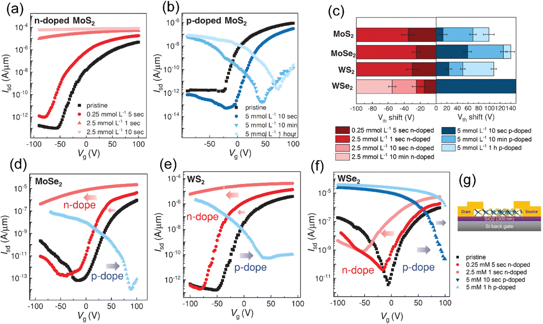 | ||
| Fig. 11 (a) Transfer characteristics (ISDvs. VG) of a pristine MoS2 FET before treatment and after consecutive n-doping with RhCp*Cp with three different concentrations/exposure times. (b) ISDvs. VG of a pristine MoS2 FET and after p-doping with MB for increasing exposure times. (c)–(e) ISDvs. VG of the remaining three MX2 FETs (MoSe2, WS2, and WSe2) before and after doping with n- and p-dopants. Treating the transistor with n-dopants shifts the threshold voltage (Vth) to more negative values, indicating n-doping (arrow). (f) Effects of different n- and p-dopants on Vth. (g) Schematic of monolayer MX2 transistor (M = Mo, W; X = S, Se). (a)–(g) Reproduced from ref. 204 with permission from Wiley-VCH, copyright 2018. | ||
The implementation of ion beam irradiation has been recognized as an potential method to engineer chemically active defects in 2D TMD materials.206 In this context, Bertolazzi et al. employed the argon-ion bombardment method to create sulfur vacancies in monolayer MoS2.206 However, a deep understanding of the effects of generated defects on the functional characteristics of MoS2 is still needed. A systematic investigation of the correlation between critical electronic device parameters and the density of sulfur vacancies is reported through the fabrication and characterization of a 1L MoS2 FET that has been exposed to a variable fluence of low-energy argon ions. Exposing both pristine and ion-irradiated FETs to vapors of butanethiol—a short linear thiolated molecule can further improve or restore their electrical properties.190,206,208,275 This solvent-free chemical treatment, investigated strictly in an inert atmosphere, eliminates secondary healing effects generated by oxygen or oxygen-containing molecules. The outcome provides valuable insights for designing optoelectronic devices based on MoS2 with a controlled density of sulfur vacancies. Furthermore, these results pave the way for introducing specific molecular functionalities using effective thiol chemistry approaches.
Another alternative method has been reported for the substitution of p-type doping in 1L to few-layer WS2 by introducing highly reactive nitrogen atoms.265 It is demonstrated that the introduction of nitrogen atoms in atomically thin WS2 induces minimal lattice distortion owing to its low kinetic energy. The separation of the A1g and 1E2g Raman peaks remains the same as that for the pristine sample, which indicates that no obvious lattice distortion was induced during the doping process. However, a noticeable peak broadening in the 1E2g phonon is found from the N-WS2 sample, which is attributed to symmetry weakening of the 1E2g phonon mode caused by the nitrogen-induced strain in WS2. The transfer characteristics of WS2 FETs clearly exhibit an n-channel-to-p-channel conversion with nitrogen incorporation. Tang et al. further explored the defect formation energy and the origin of p-type conduction by first-principles calculations.198 In nitrogen-doped WS2, defect state emerges near the Fermi level, resulting in a shallow acceptor level located above the valence band maximum. By employing this doping strategy, it becomes possible to achieve substitutional p-type doping in intrinsically n-type TMDs. The process allows for the precise control of dopants, presenting an avenue for creating complementary metal-oxide-semiconductor FETs and optoelectronic devices on 2D TMDs. This approach overcomes one of the main limitations of TMDs, namely, their n-type unipolar conduction.265 Kappera et al. introduced a novel phase engineering approach to achieve low-resistance contacts and enhance the performance of FETs based on ultrathin MoS2.276 They have further established a methodology to fabricate metallic 1T phase patterns on ultrathin semiconducting MoS2 nanosheets and used them as electrodes. The low contact resistances of 200–300 Ω μm at zero gate bias are attributed to the atomically sharp interface between the phases and the similarity in work function of the 1T phase and the conduction band energy relative to the vacuum level of the 2H phase (approximately 4.2 eV) (Fig. 12h–i). Both top-gated and bottom-gated devices employing 1T phase electrodes exhibit superior performance when compared to devices with direct metal contacts to the semiconducting 2H phase. The measured properties in air indicate mobility values of approximately ∼50 cm2 V−1 s−1, subthreshold swing (SS) values of 90–100 mV decade−1, and current on/off ratios of >107.276 Additionally, the performance of devices with 1T electrodes is remarkably reproducible and remains independent of the type of contact metal pads used.
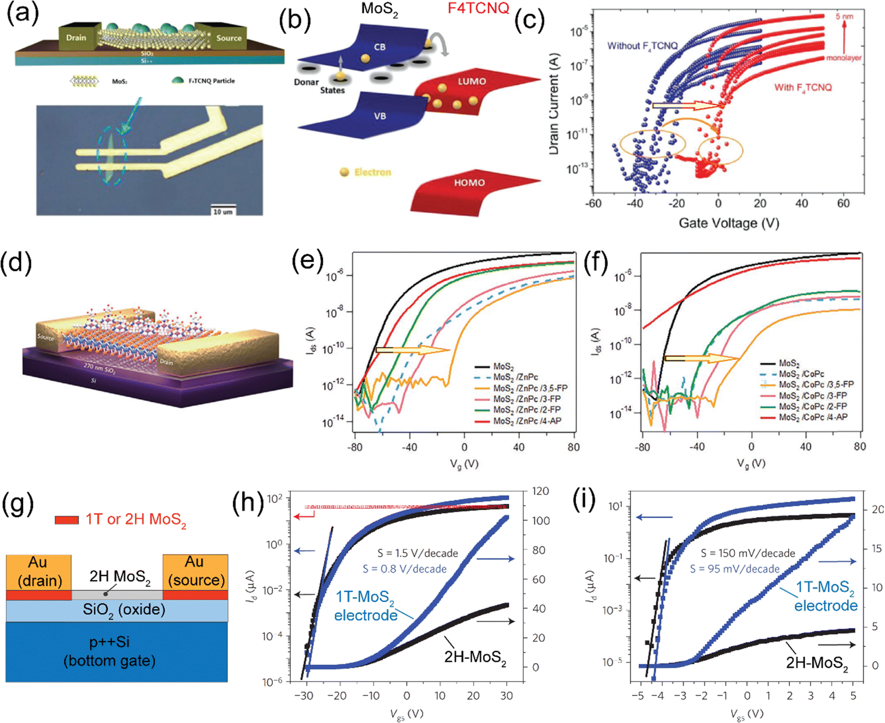 | ||
| Fig. 12 (a) Schematic of the MoS2 FET with F4TCNQ-coated nanoparticles. (b) Energy band diagram at the vdW interface between MoS2 and F4TCNQ. (c) IDSvs. VGS of MoS2 FETs with and without F4TCNQ. (d) Device schematic of MoS2 functionalized with MPc/fPy. (e) Comparison of transfer curves of MoS2/ZnPc heterojunction coordinated with ligands. Comparison of IDSvs. VGS of MoS2/CoPc heterojunction coordinated with ligands. (f) Comparison of transfer curves of MoS2/CoPc heterojunction coordinated with ligands. (g) Schematic of 1T phase electrodes and Au electrode on the 2H phase. (h) and (i) Transfer characteristics with 1T and 2H contacts, respectively. (a)–(c) Reproduced from ref. 114 with permission from Wiley-VCH, copyright 2018. (d)–(f) Reproduced from ref. 69 with permission from Wiley-VCH, copyright 2020. (h)–(i) Reproduced from ref. 276 with permission from Nature Publishing Group, copyright 2014. | ||
5.3. Anti-ambipolar FET
An atomically thin TMD partially screened electric fields when applied perpendicularly to the monolayer, leading to the development of ‘gate-tunable’ TMDO p/n heterojunction diodes for potential use in high-speed communications circuits, for example, pentacene/MoS2 and CuPc/MoS2.97,102 Furthermore, applied voltages can be employed to control extended defects like grain boundaries in monolayer TMDs.As a result, this leads to the production of gate-tunable memristor devices, showing great promise as fundamental building blocks for ‘non-volatile’ computer memory and neuromorphic (brain-like) circuit architectures.277 Due to the atomically thin nature of MoS2, the junction displays gate-tunability with an asymmetric anti-ambipolar transfer characteristic.133 Through the utilization of spatial photocurrent mapping and surface potential profiles, along with finite element simulations, it has been confirmed that there is band bending occurring in both the lateral and vertical directions in type-II band alignment. The type-II alignment induces a built-in potential, resulting in the rectification of IDS–VDS (output) characteristics at different VG values. In the pentacene/MoS2 heterojunction, VDS represents the bias applied to the pentacene electrode (electrode 3 in Fig. 13a), where VDS > 0 corresponds to the forward bias, while the MoS2 electrode is grounded. The heterojunction exhibits a transition from nearly insulating behavior at extreme VGS values (VGS = 60 V and VGS = −80 V) to highly rectifying output characteristics at intermediate values. The transfer plots depicted in Fig. 13c provide additional evidence of the gate-tunability of the current through the p–n heterojunction. Notably, the transfer curve of the heterojunction (green) exhibits an anti-ambipolar response, which is also observed in inorganic p–n junctions.278–280 In contrast to earlier devices featuring symmetric transfer characteristics, the pentacene/MoS2 heterojunction demonstrates asymmetric transfer characteristics with different transconductances on either side of the IDS peak. The observed asymmetry in the anti-ambipolar transfer characteristic presents promising opportunities in emerging circuit applications. It has the potential to be effectively utilized for simultaneous phase and amplitude shift keying in wireless telecommunication technologies.97,281 Velez and their group presented experimental findings on a CuPc/MoS2 hybrid p–n junction, revealing its gate-modulate diode characteristics and photovoltaic effects.102 In Fig. 13f, the transfer curves of the CuPc/MoS2 device are displayed at different Vds values. The transfer curve exhibits a characteristic shape that remains consistent for all Vds values, demonstrating an asymmetry originating from the small subthreshold swing.269 The p–n junction devices based on monolayer MoS2 yield similar curves. Remarkably, efficient gate control over the heterostructure is consistently achieved. This capability is directly associated with the use of thin MoS2 flakes, whether monolayers or bilayers, which facilitates the extension of the electric field from the gate into the CuPc layer.
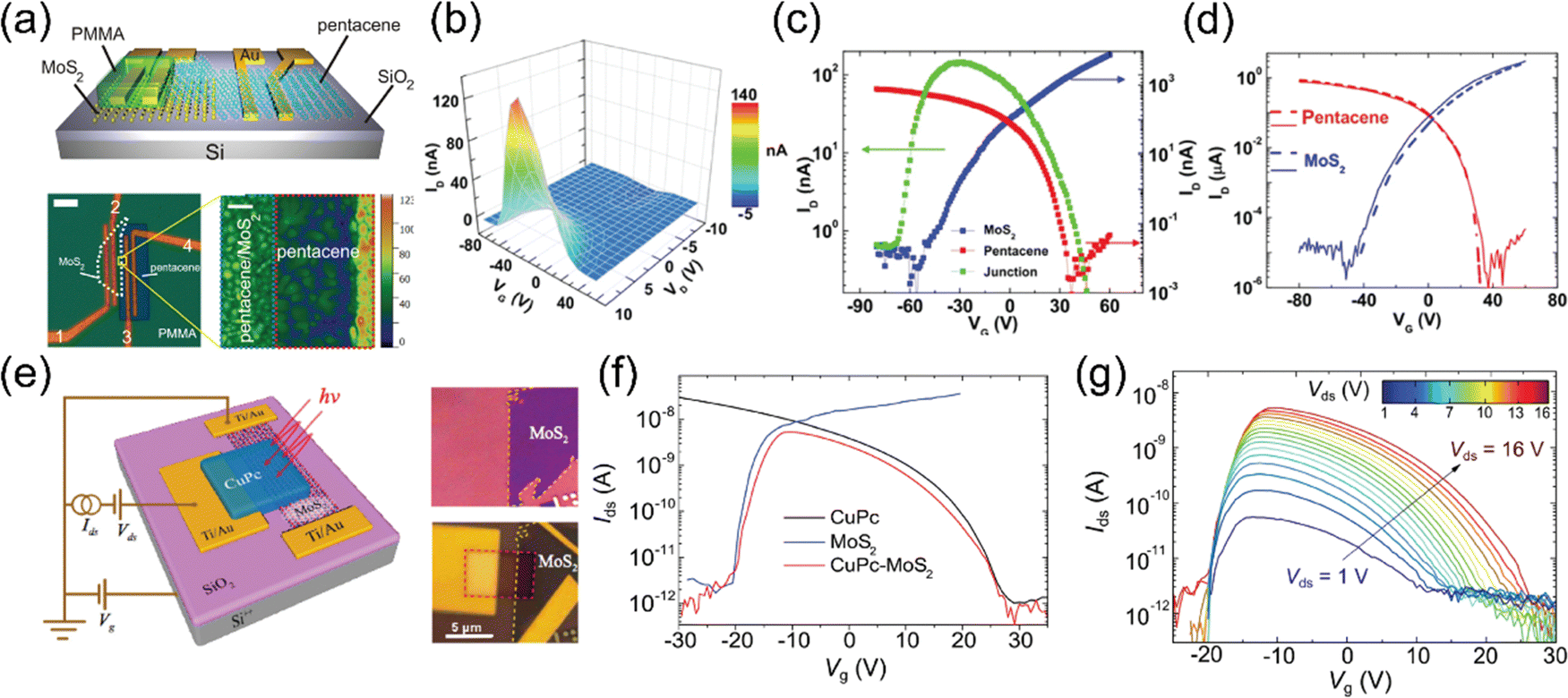 | ||
| Fig. 13 (a) Schematic of the pentacene/MoS2 p–n heterojunction, and optical and AFM micrographs of a representative device. Electrical properties of the pentacene/MoS2 anti-ambipolar p–n heterojunctions. (b) Gate-dependent IDS–VDS output characteristics of a representative device. (c) IDSvs. VGS of the pentacene (VDS = 10 V) and MoS2 (VDS = 1 V) FETs as well as the junction (VDS = 10 V). The junction transfer curve shows an asymmetric anti-ambipolar characteristic. (d) Simulated (dashed lines) and experimental (solid lines) transfer characteristics of pentacene and MoS2 FETs. (e) p/n junction CuPc/MoS2 device. (f) Transfer curves (Idsvs. Vg) measured in CuPc/MoS2 FET at Vds = 16 V, in the MoS2 bilayer of the same device at Vds = 5 V and in a CuPc transistor produced on the same wafer at Vds = 16 V. (g) Idsvs. Vg of the CuPc/MoS2 device measured at different Vds. (a)–(d) Reproduced from ref. 97 with permission from American Chemical Society, copyright 2022. (e)–(g) Reproduced from ref. 102 with permission from Royal Society of Chemistry, copyright 2015. | ||
5.4. Phototransistors
The operation of a phototransistor relies on the photogating effect, where a gate bias is applied to modulate current. This modulation process resembles that of a conventional FET structure. However, phototransistors differ in their ability to effectively detect electrical signals resulting from alterations in source-drain current or shifts in the transfer curve due to gate bias changes when exposed to light.105,250,282 Evaluating the performance of phototransistors in light sensing applications involves considering several crucial parameters. These parameters encompass photoresponsivity (R), photosensitivity (P), detectivity (D), and external quantum efficiency (EQE), each playing pivotal roles in assessing their effectiveness. For a more in-depth examination of these parameters and their significance, several articles can be referred.283,284 In particular, photoresponsivity (R) stands out as a key metric for gauging phototransistor performance, and its determination relies on the analysis of transfer characteristics. The formula for calculating R is provided by eqn (4):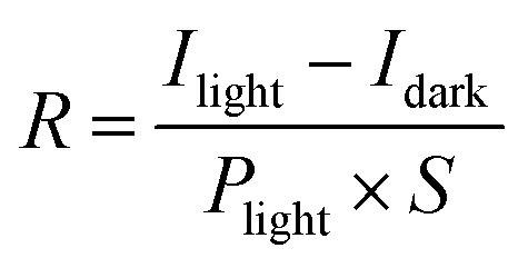 | (4) |
 | (5) |
 | (6) |
The visible range of the direct bandgap offers effective light absorption and luminescence capabilities, which allow a MoS2-like TMD gap semiconductor to be used as a channel material for phototransistors. However, in atomically thin semiconductors, the total photocarrier generation efficacy is limited by the level of optical absorption. When organic semiconductor is combined with layered TMD semiconductor, the monolayer TMD typically led to a higher optical absorption than any TMD heterostructures.17,23,144 TMD-based phototransistors can suffer from persistent photoconductance, failing to turn off when the light is removed due to charge trapping at the substrate/TMD interface and inherent trap states in thin materials. To address this, molecular systems forming type II alignments with TMDs have been employed. These systems quickly dissociate photoexcited charges through the built-in potential at the type II interface, enabling a swift photoresponse.254,267,285
TMDO hybrids outperform pristine TMDs by promoting spontaneous charge transfer across layers, enhancing electrical currents. Additionally, carefully chosen organic systems can absorb a broad spectrum of light, enabling TMDO phototransistors to operate over a wide range of wavelengths. The combination of 2D-TMDs with organic semiconducting crystals in heterostructures offers exciting possibilities for the fabrication of diverse hybrid devices such as phototransistors.282,285,286 It has been recently reported that thiol-based modification enhances electrical and optical performance in multilayer MoS2. Two types of thiol-terminated organic molecules, namely, 4-amino thiophenol (4ATP) and 4-nitro thiophenol (4NTP) are used for electron-donating and electron-withdrawing effects, respectively.268 These molecules chemically bond with MoS2, with 4ATP boosting the current and carrier concentration and 4NTP reducing the film conductance. In Fig. 14b, the 4ATP-MoS2 transistor exhibits a higher drain current (IDS) than that of the pristine case, and the threshold voltage (VTH) shifts negatively from −19.6 V to −49.9 V after 24 hours. Further, Fig. 14c shows time-resolved photoswitching IDS curves for pristine and 4ATP-MoS2 transistors (VGS = 0 V). The photoswitching characteristics are suitable, with increased Iph due to enhanced I0 after functionalization. Additionally, they modulate MoS2 transistor photoresponsiveness, with 4ATP enhancing photoresponsivity (≈669 A W−1) and 4NTP improving photoswitching.268 Thiol-based functionalization effectively tailors multilayer MoS2 electrical and optical properties. Besides functionalization, CuPc molecules boosted the MoS2 performance in CuPc/MoS2 hybrid structures, increasing the photoresponsivity and photodetectivity tenfold. The hybrid achieved an EQE of 12%, over twice that of pristine MoS2, demonstrating superior performance in the visible spectrum. Molecular systems enhance the quantum efficiency and speed up photoresponse in TMD phototransistors.254
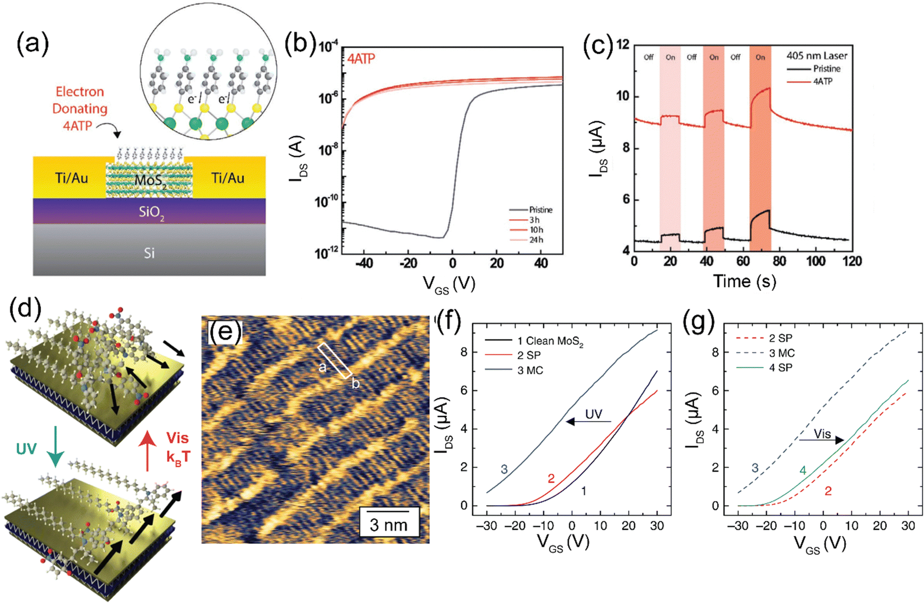 | ||
| Fig. 14 Phototransistor: (a) device structure (inset: details of electron transfer at the interface). (b) Transfer curves. (c) Time-resolved photoswitching IDS curves. Photo-switchable superlattice: (d) schematic representation of the molecular dipoles (black arrows) are randomly oriented before irradiation, yet well aligned after UV irradiation. (e) STM images of the merocyanine (MC) assembly on MoS2. (f) IDSvs. VGS curve: trace 1 (black) for clean MoS2, trace 2 (red) for MoS2 covered by the SP layer, trace 3 (blue) for MoS2/MC after UV irradiation over the whole flake. (g) Trace 4 (green) for the pristine MoS2/SP trace can be recovered upon irradiation of the whole surface with green light. (a)–(c) Reproduced from ref. 268 with permission from Wiley-VCH, copyright 2021. (d)–(g) Reproduced from ref. 62 with permission from Nature Publishing Group, copyright 2018. | ||
A recent investigation has demonstrated the development of highly sensitive light detection phototransistors based on a fully ordered organic SAM incorporated into hybrid organic–inorganic van der Waals (vdW) heterojunctions.287 Incorporating a SAM as the bottom layer offers many advantages: (i) the SAM allows precise control over the long-range ordered molecular film, achieving a single molecular thickness,288 effectively minimizing charge scattering and recombination as compared to multilayer organic films;289 (ii) the processing method involving adsorption from a solution is straightforward;22 and (iii) BTBT-SAM enables efficient two-dimensional lateral π–π interactions for effective charge transfer.288 The heterojunctions, formed by monolayer MoS2 onto organic BTBT SAM, are studied by Raman and PL spectroscopy along with Kelvin probe force microscopy. Remarkably, this heterojunction transistor displays an exceptional photoresponsivity reaching 475 A W−1 and an enhanced external quantum efficiency of 1.45 × 10⁵%. Additionally, it exhibits an exceedingly low dark photocurrent in the pA range.287 It is further demonstrated that the hybridization of SAMs with TMD materials holds great promise for creating a wide range of optoelectronic devices with distinctive properties. Phototransistors offer numerous design possibilities for stacking and integrating 2D TMD atomic-molecular layers by manipulating the SAM structures. This novel heterostructure shows exciting potential for advanced optoelectronic devices.
5.5. Photo-switchable superlattices
Molecular switches facilitate the development of multifunctional devices, wherein an electrical output can be influenced by external stimuli. However, proving the operational mechanism of these devices often poses challenges, as the molecular switching events are indirectly confirmed through electrical characterization without direct real-space molecular-scale visualization. In a recent study, Gobbi and co-workers62 demonstrated multi-responsive devices that rely on the collective switching action of photochromic molecules self-assembled on the surface of TMDs. They unveiled the mechanism by introducing a method to optically modulate the electrical properties of versatile hybrid devices, utilizing photochromic SP and MoS2 superlattices. They achieved this by creating supramolecular assemblies of photochromic spyropyrans (SP) on the surfaces of monolayer MoS2, enabling the investigation of light-induced changes in physicochemical properties on a macroscopic scale (see Fig. 14e). After inducing SP/merocyanine (MC) isomerization with UV light, they observed a significant reduction in the work function of the underlying materials. Conversely, exposure to visible light triggered MC/SP isomerization, nearly fully restoring the work function of the material. This demonstrated their ability to exercise optical control over the local charge carrier density in high-performance transistors through a comprehensive study that integrated sub-nanometer-resolved STM investigation and characterization of mesoscopic devices (as shown in Fig. 14e). Their STM imaging findings aligned well with the results obtained from molecular dynamics simulations and density functional theory calculations. They successfully showcased the ability to adjust the threshold voltage in MoS2 transistors by exposing them to UV-visible light at the heterojunctions between inorganic surfaces and 2D supramolecular networks (as depicted in Fig. 14f and g).62 This work's notable achievement lies in the direct visualization of structural changes at the molecular level accompanying photoisomerization. By precisely manipulating the electrical characteristics of 2D vdW material devices through ultra-high spatial resolution molecular switching, they have created opportunities for tailored adjustments in the electrical output of organic–inorganic heterojunction devices, offering promising prospects for multifunctional sensors and optoelectronic applications.A similar level of control over switching events and molecular assembly has been previously demonstrated in dynamic molecular crystals. These dynamic molecular crystals refer to self-assembled crystalline structures, usually three-dimensional, where macroscopic structural changes originate from collective molecular events.290–292 However, bulk dynamic molecular crystals are generally poor electrical conductors and unsuitable for macroscopic device operation. This limitation arises due to the chemical structure of molecular switches, which is not optimized for efficient charge transport. In this regard, by adopting this approach, it becomes feasible to incorporate a functional supramolecular assembly, representing the quasi 2D limit of molecular dynamic crystals, into high-performance devices capable of exhibiting switchable electric outputs.
Moreover, future optical, electrical, and quantum information applications revolve around newly emerging quantum phenomena in electronically coupled two-dimensional heterostructures. Such processes could be controlled by tailoring the electronic band gaps in coupled heterostructures, which is of great research interest. vdW heterostructures made of atomically thin materials of TMDs have emerged as another promising platform for studying correlated electronic phenomena with highly tunable parameters.293 These layered materials can be assembled into non-covalently bonded heterostructures without the lattice matching results electronic interaction is maximization. Such a superposition of the TMD layer often gives rise to an interference effect known as the moiré pattern.294,295 Such regions in the moiré pattern appear dark in the STM images due to the reduced density of states near the Fermi level. This pattern defines a superlattice, which has a periodicity larger than that of either of the individual lattices. This in-plane superlattice induces local variations in the heterostructure's electronic structures, leading to the formation of minibands.296,297 This effectively enhances the effective mass of the charge carriers and makes correlation effects more prominent in such vdW heterostructures.298 In this regard, 2D TMD represents an ideal platform to study the interplay between the molecular assembly on surfaces and electrical transport in devices. On the exposed surface of 2DMs, well-defined molecular groups can be arranged at predetermined spatial locations with atomic precision by tailoring of molecular architectures.62
5.6. A recent advent: multifunctional synaptic FET
Biological synapses are integral components of the nervous system, serving as essential elements for computing and memory functions in the human brain. In artificial neuromorphic systems, synaptic devices play a pivotal role as fundamental building blocks for constructing neuromorphic networks (see schematic Fig. 15a–c). Therefore, the advancement of novel artificial synapses holds paramount importance in the field of neuromorphic computing.300,301 In a nervous network, the synaptic weight defined as the connection strength between presynaptic neuron and postsynaptic neuron can be modulated by action potentials, which have been well discussed in a recent review.302–304 Synaptic plasticity, a fundamental neurobiological phenomenon, is crucial for memory and learning processes in the brain, enabling the implementation of intricate brain functions. It encompasses two key components: short-term plasticity (STP) and long-term plasticity (LTP). These mechanisms play vital roles in shaping the efficiency and adaptability of neural circuits.305 STP stored in the hippocampus is characterized by a temporal change in synaptic connections, which rapidly decays to its original state after the removal of an external spike. STP is essential for efficient information processing in neural circuits.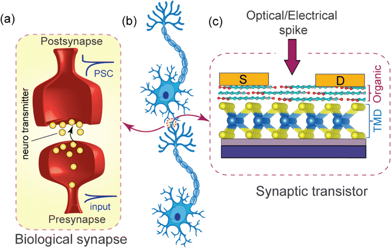 | ||
| Fig. 15 TMDO hybrid heterojunctions constituting a multifunctional artificial synaptic transistor. (a) Biological synaptic diagram: electrical or optical spikes serve as a presynaptic input spike and a source–drain channel current as stimulated postsynaptic current. (b) Simplified illustration of a biological synapse. (c) TMDO hybrid heterojunction constituting a multifunctional artificial synaptic transistor. | ||
When a potential pulse is applied to the presynaptic membrane, it triggers the release of neurotransmitters, resulting in a change in the postsynaptic current. Excitatory postsynaptic current (EPSC) occurs when excitatory neurotransmitters are released and results in the strengthening of the synaptic weight. However, inhibitory postsynaptic current (IPSC) occurs when prohibiting neurotransmitters are released, and results in the weakening of synaptic weight. Paired-pulse facilitation (PPF) is one of the typical STP behaviors, which describes the fact that an enhanced postsynaptic response is obtained by the consecutively applied pair of presynaptic spikes. In contrast, LTP represents a longstanding transformation in synaptic connections, playing a crucial role in memory and learning processes. Through repetitive rehearsal, STP can be converted into LTP.306,307 Further, simulating synaptic short-term plasticity (STP) and long-term potentiation (LTP) behaviors using unique artificial devices, like inhibitory post-synaptic current (IPSC), excitatory post-synaptic current (EPSC), paired-pulse depression (PPD), paired pulse facilitation (PPF), and spiking-rate-dependent plasticity (SRDP), holds great promise. These devices play a crucial role in advancing the development of neuromorphic computation, enabling the study and implementation of complex synaptic responses and facilitating memory and learning processes akin to those observed in biological systems. In addition, LTP in synaptic devices provides a physiological substrate for learning and memory, whereas STP supports a variety of computations. It is worth noting that organic bioelectronics have gained intense interest in neural applications due to their low-cost processing, availability of a virtually infinite number of molecules with multifunctional optoelectronic properties, tenability and mechanical flexibility. Furthermore, because of their unique internal and interfacial structures, and electrical and optical properties,308,309 2D-TMDs such as MoS2 and WSe2 have been reported as potential candidates for complex neuromorphic applications. Recently, Wang and coworkers have demonstrated the first multifunctional artificial neural synapse transistor fully based on 2D-TMDs and organic layers, that is, MoS2/PTCDA hybrid heterostructures with neuromorphic functions of STP and LTP including IPSC, EPSC, PPD, PPF, and SRDP, which can mimic some crucial behaviors of biological neurons.310
By carefully designing the energy band structure, the system achieves both robust electrical and optical modulation modes. The gate-tunable band alignment of such a type-II heterojunction allows the carriers to be both electrically and optically injected into MoS2, separated and captured at the heterojunction interface and gradually released to simulate the basic functions of biological synapses. They have reported the synaptic inhibition and excitation simultaneously by efficient modulation of the gate voltage in a single device. It exhibits a threshold voltage (Vth) drift window of 6 V in a static direct-current transfer curve. Notably, it exhibits a minimum inhibition of 3% and a maximum facilitation ratio of 500% by increasing the number of gate electrical pulses. Additionally, the device's response to varying frequency voltage signals demonstrates dynamic filtering capabilities, making it an efficient means for information transmission within an artificial neural network during electrical modulation. In the realm of optical modulation, this device demonstrates remarkable flexibility in tuning short-term potentiation (STP) and long-term potentiation (LTP). The long-term synaptic weight change (ΔW/W) achieved in this mode is notably improved, reaching up to 60, surpassing the results reported in other works. In the optical modulation mode, a very good flexible tunability of STP and LTP is reported and the long-term synaptic weight change (ΔW/W) is greatly improved, reaching up to 60, compared to the results reported in other works.310–313 Moreover, upon comparing the optimal performance parameters of MoS2/PTCDA devices, they exhibit remarkable superiority when compared to other artificial synaptic devices based on 2D materials, whether they are organic or inorganic in nature.122,271,313–327 The acceptable power consumption of 10 pJ is 90 times smaller than the conventional CMOS and close to the human brain.316,328 Therefore, the multifunctional artificial synaptic transistor based on the TMDO hybrid heterojunction is a promising candidate for constructing a neuromorphic system. It paves a whole new and efficient path for building neuromorphic system hardware elements.
They observed synaptic behavior by applying a presynaptic Vcg voltage pulse while maintaining Vbg constant (Fig. 16a and 2b). Prior to the Vcg pulse, Ids of the MoS2/PTCDA synaptic transistor remained stable over time, corresponding to stage I. During the 25 ms Vcg pulse, Ids underwent modulation via electrostatic doping. Depending on the pulse (positive or negative), Ids was either suppressed (Fig. 16a) or enhanced (Fig. 16b), corresponding to stages II and IV, respectively. Importantly, after the pulse cessation, Ids did not return monotonically to the reference level. Instead, following a relatively positive (negative) Vcg voltage pulse, it settled at a lower (higher) level relative to the reference, resembling postsynaptic current behavior with a slow relaxation phenomenon. This corresponds to stages III and V, manifesting as synaptic IPSC and EPSC behaviors, respectively. As shown in Fig. 16c, the positive Vcg pulses (−12 V, 25 ms) applied at Δt = 25 ms lead to a further suppression of the postsynaptic current magnitude, resulting in A2 < A1, as indicated in the gray portion. Conversely, Fig. 16d shows that negative Vcg pulses (−20 V, 25 ms) enhance the postsynaptic current magnitude (A2 > A1), corresponding to synaptic PPD and PPF behaviors, respectively. Further, the synaptic transistors based on MoS2/PTCDA hybrid heterojunctions can also operate in the optical modulation mode due to the strong light absorption (served as input gate signal) capability of both MoS2 and PTCDA. A characteristic EPSC response is observed when the MoS2/PTCDA transistor is subjected to a pair of laser pulses. The laser pulses have a pulse width of 400 ms with an interval of 100 ms, and Vds is set at 0.1 V (the green area represents laser pulse irradiation). This results in a higher excitation current amplitude (A2 > A1), as shown in Fig. 16e. The inset depicts the phenomenon that the optically modulated PPF ratio (A2/A1) decreases as a function of Δt. It shows a decrease in the PPF ratio with increasing Δt, eventually stabilizing around 100%. The maximum value of the PPF ratio is achieved at the minimum time interval Δt of 25 ms, reaching a value of 147%. The artificial synaptic behavior induced by the transfer and exchange of internal charge carriers in the heterojunction under electrical and optical modulation indicating a stronger synaptic plasticity (STP and LTP) is promising. The observed phenomenon exhibits striking similarity to the process of neurotransmitter release observed in biological synapses.
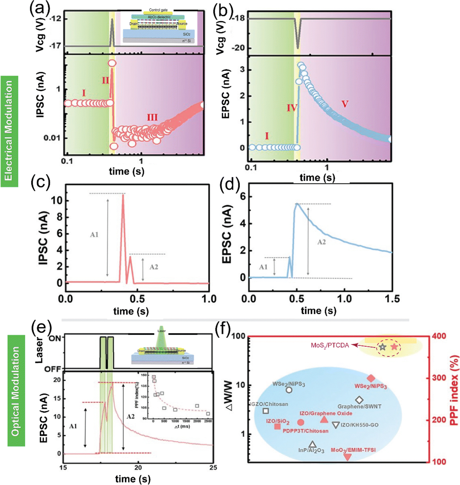 | ||
| Fig. 16 Artificial inhibitory and excitatory synaptic behaviors based on the MoS2/PTCDA hybrid heterojunction in the electrical modulation mode. (a) IDS of the MoS2/PTCDA synaptic transistor exhibits time-dependent behavior (bottom panel) in response to a relatively positive Vcg pulse (top panel). The response can be classified into three distinct stages (I, II, and III). (b) Upon the application of a relatively negative Vcg pulse, a series of EPSC behaviors can be divided by distinct stages labeled as I, IV, and V. (c) IPSC behavior when stimulated by a pair of relatively positive Vcg pulses, with pulse intervals of 25 ms. (d) EPSC behavior when subjected to a pair of Vcg pulses, with a pulse interval of 25 ms. This phenomenon enables an optical transition from STP to LTP, facilitating the long-term modulation of synaptic weight in the device. (e) EPSC of the MoS2/PTCDA transistor is triggered by a pair of laser pulses. Pulse width = 400 ms, interval = 100 ms, and Vds = 0.1 V; the green area represents the irradiation of the laser pulses. The inset shows the PPF index A2/A1 (black hollow square) as a function of laser pulse. (f) Statistical comparison of the synaptic weight changes and PPF ratio with other reported works. (a)–(f) Reproduced from ref. 138 with permission from Wiley-VCH, copyright 2018. | ||
In neuroscience and computer science, synaptic weight represents the strength or amplitude of the connection between two nodes, elucidating the extent to the stimulation effect of a specific neuron on other neurons within biological systems.329 Changes in synaptic weight are recognized as synaptic plasticity;330,331 however, the underlying mechanism responsible for long-term alterations remains uncertain. The long-term synaptic weight change is defined as ΔW/W = (I − I0)/I0, where I and I0 are the steady-state base postsynaptic currents before and after laser pulses, respectively. With the increase in the number of laser pulses, synaptic weight changes can be effectively increased, and long-term synaptic weight changes are able to further strengthen via varying Vbg, which is consistent with the transition from STP to LTP. In other words, enhancing the synaptic connections is consistent with the long-term memory effects of the biological nervous system. Remarkably, a significant long-term synaptic weight change of up to 60 has been achieved.138Fig. 16f exhibits the statistics and comparison of synaptic weight changes and PPF ratios with various heterostructures. Additionally, comparing the optimal performance parameters of novel MoS2/PTCDA heterostructure devices reported superiority to that of the other 2D-based artificial synaptic devices. Therefore, it is possible to fabricate new, novel, and promising synapse element-based TMDO hybrid heterostructure transistors. Again, TMDO-based devices with superior and flexible versatility are used as artificial neural network chip units, which is of great significance for constructing artificial neural network systems. Further, the device has a robust dual electrical and optical modulation mode of operation, making it highly desirable for neural network applications, thereby overcoming challenges related to implementing these functionalities within a single device. In summary, based on the powerful dual mode of operation, the system operation of synaptic STP and LTP in the device could be achieved. Therefore, TMDO demonstrates that it has tremendous potential for application in neuromorphic computation.
6. Photodetector
For photodetection, the layered 2D-TMD-based photodetectors have been demonstrated with very high responsivity and fast photoresponse.332–334 Beyond the structures of MoS2 FET alone, it is reported that through stacking of other materials, MoS2-based heterostructures can exhibit a higher photoresponsivity.23,254,335,336 The development of TMDO heterostructures is required to lower the recombination rate of carriers and to reduce the metal–semiconductor contact resistance, which should lead to an improved performance of TMD-based electronic and optoelectronic devices such as photodetectors. The challenging issue for MoS2 devices exists due to their persistent photoconductance (PPC),333 which has been debatably ascribed to the minority carrier trapping by surface absorbents, inherent trap states in MoS2, and the neighboring dielectrics.337,338 Although such minority carrier trapping can improve the gain mechanism in detectors by lengthening the apparent carrier lifetime, a dramatic sacrifice in the response speed occurs in devices since the PPC effect often lasts from minutes to hours. Attempts to improve the response dynamics, e.g., using surface passivation and field-effect methods that modulate the density of trap states and their occupation, however, often leads to the loss of sensitivity due to the adverse suppression of trap-induced gain mechanisms.105In present, the ultrafast photoresponse dynamics was achieved in monolayer MoS2 detectors by the surface assembly of ZnPc organic molecules.105 It is found that the assembly of ZnPc molecules tends to compensate the intrinsic electron doping in MoS2 by withdrawing electrons from MoS2. Such charge transfer contributes to a spontaneous reverse separation of electron–hole pairs under light illumination, driving holes to ZnPc molecules. This is found to favorably suppress the rather slow minority carrier trapping to the inherent trap states in MoS2 and the substrates, providing an accelerated response speed (<8 ms) compared to that of bare MoS2 (20–40 s). The fast photoresponse dynamics here is further demonstrated to endure tailorable engineering of the device responsivity (0.92–7.84 and further to 880 A W−1) when using external gate modulation via Al2O3 passivation, manifesting the special promise of vdW-coupled molecules on 2D TMDs for high-performance photodetection.
The field-effect transfer curves for the same MoS2 device before and after varied ZnPc treatments (10, 40 min) were first measured, as shown in Fig. 17a–d. The measurements were conducted both in the darkness and under illumination (3.64 mW cm−2) using a Vds value of 1.6 V. As displayed in Fig. 17b, the measured transfer curves for all devices manifest the n-type conduction with electrons as the majority carriers. Increasing the ZnPc treatment leads to a decrease in the source–drain current (Ids) and a positive shift of the threshold voltage (Vth), which are consistent with the electron compensation effect of ZnPc molecules to MoS2. After 40 min of ZnPc treatment, one witnesses the emergence of bipolar characteristics (p-type at Vg < 20 V, n-type at Vg > 5 V) in MoS2 under dark conditions. However, under light illumination, the samples again display n-type conduction with considerably negatively shifted threshold voltages of less than −15 V. This phenomenon suggests the intense n-type photodoping effect in MoS2 by the preferential trapping of photogenerated holes compared to electrons.262,333,338Fig. 17c shows the dark and photo current–voltage characteristics for both the bare and ZnPc-treated MoS2 devices. A transition of current–voltage characteristic from nonlinear to linear behavior is found when the devices are switched from darkness to illumination. Such a change is related to the reduced Schottky barrier heights (SBHs) at the contacts by the significantly increased electron concentration in MoS2 due to the pronounced photodoping.21,105,339
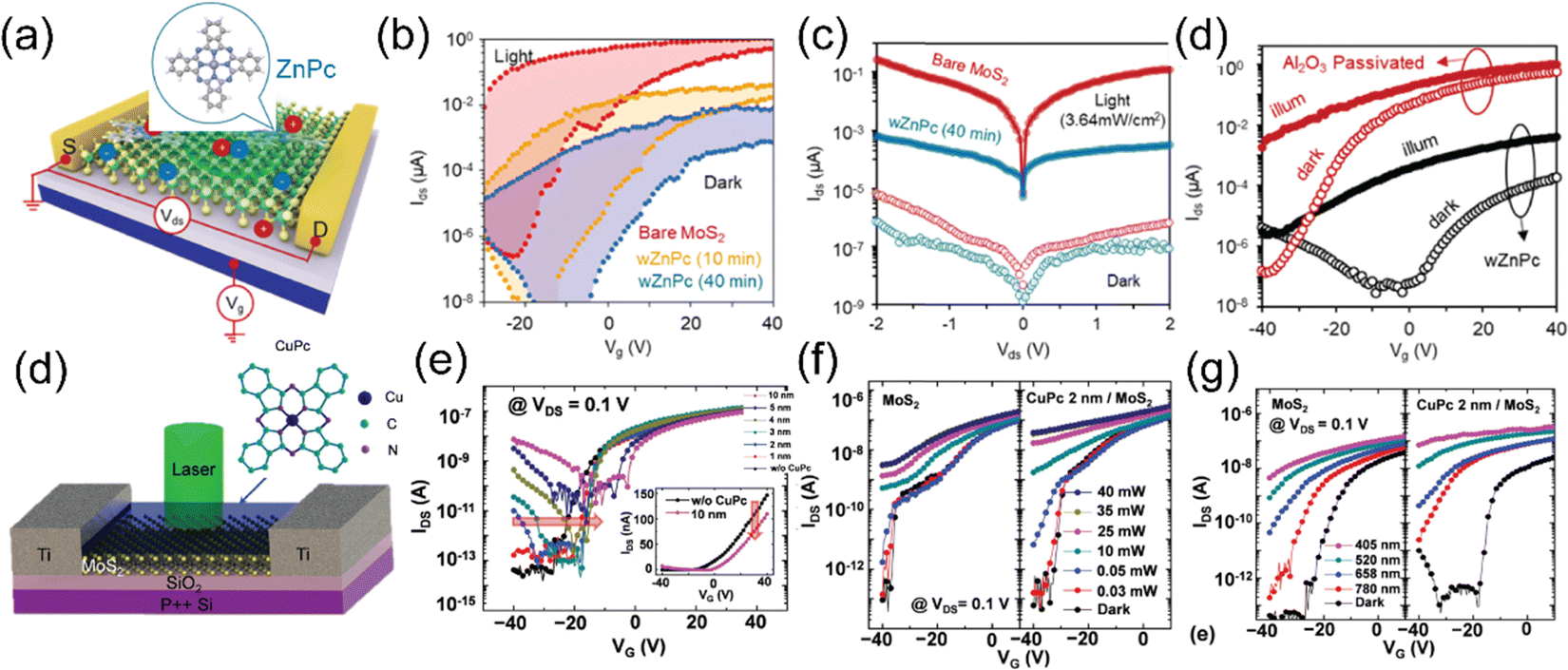 | ||
| Fig. 17 (a) Schematic of a FET device with a flat-lying ZnPc molecule on 1L MoS2. (b) IDS–VG characteristics for a MoS2 device after varied ZnPc treatments in the darkness and under illumination (532 nm, 3.64 mW cm−2). (c) Dark and photo current–voltage characteristics for both the bare and ZnPc-treated MoS2 devices. (d) Transfer curves and transient photoresponse characteristic of the device before and after Al2O3 passivation. (e) Schematic of the CuPc/MoS2 device illuminated by a laser. The molecular structures of the CuPc are also indicated. (f) IDS–VG curves on the semilogarithmic scale of the MoS2 devices without (labeled with “w/o CuPc”) and with CuPc layers of various thicknesses (1, 2, 3, 4, 5, and 10 nm) measured at a fixed VDS = 0.1 V. The inset is a linear plot of IDS–VG curves for a pristine MoS2 device without a CuPc layer and a 10 nm-thick CuPc/MoS2 hybrid device. Arrows indicate shifts in threshold voltages and currents. (g) Photocurrent of pristine MoS2 and CuPc/MoS2 photodetectors measured at VG = −40 V and VDS = 0.1 V as a function of the laser intensity. (h) IDS–VG curves of pristine MoS2 and CuPc/MoS2 photodetectors measured in the darkness and under illumination conditions at different wavelengths and a fixed laser power (40 mW) (adapted from ref. 187). (a)–(d) Reproduced from ref. 105 with permission from American Chemical Society, copyright 2018. (d)–(g) Reproduced from ref. 254 with permission from Royal Society of Chemistry, copyright 2015. | ||
Furthermore, an additional study demonstrates favorable photo-responsive characteristics of MoS2 FET by incorporating a p-type organic copper phthalocyanine (CuPc) layer on the MoS2 surface (see Fig. 17e–h).254 Specifically, the CuPc/MoS2 hybrid devices demonstrated superior photodetection capabilities when compared to pristine MoS2 FETs, owing to enhanced electron–hole pair separation at the interface. The stacking of CuPc layers on MoS2 FETs allows for the control of the threshold voltage through a charge transfer phenomenon occurring at the interface. Fig. 17f shows the photoresponsive data of both the pristine MoS2 FET and CuPc/MoS2 FETs measured at VGS = −40 V, while VDS = 0.1 V is constant under two different conditions: in the darkness and under laser illumination. The experiment involved illuminating the devices with light of different wavelengths (405, 520, 658, and 780 nm) while maintaining a constant power of 40 mW. The results indicated that the photoinduced current exhibited an increment as the incident light's wavelength decreased. This observation suggests that incident light with energies higher than the band gap of CuPc and MoS2 facilitates a more efficient generation of electron–hole pairs within the material. Moreover, by optimizing the CuPc thickness to approximately 2 nm on the MoS2 surface, the photodetector demonstrated superior performance. It exhibited a photoresponsivity of approximately 1.98 A W−1, a detectivity of around 6.11 × 10¹⁰ Jones, and an external quantum efficiency of about 12.57%. This study proposes that the vertical hybrid structure, fabricating 2D-TMDs like MoS2 with organic materials, holds great promise for the development of efficient photodetecting devices and optoelectronic circuits.254
It is essential to mention that while graphene has been investigated for phototransistors in photosensitive devices, it exhibits limitations in photoresponsivity (∼6 mA W−1) owing to its low light absorption coefficient and fast photoinduced carrier recombination rate.340 On the contrary, photodetectors utilizing MoS2 have demonstrated outstanding photo-response characteristics.254 For instance, devices incorporating single- and multilayer MoS2 films have shown photoresponsivities reaching 880 A W−1 and approximately 0.1 A W−1, respectively.163,334 Due to their relatively large light capture cross-sections, organic semiconductors combined with 2D-TMD materials show great potential in enhancing the performance of photodetection and photovoltaic performances.
7. Challenges and future perspectives
By giving increasing importance to TMDO hybrid heterostructures both in fundamental science and for promising applications, these hybrid materials will advance rapidly and have transformative impacts in the area of materials science. While recently there has been notable progress in the fabrication, transport properties, and applications of optoelectronic devices, there remains a need for further improvements in their performance to make them suitable for real-life applications. There are many opportunities in TMDO systems; however several limitations and related challenges remain unaddressed.i. From the viewpoint of synthesis and fabrication: the stability of monolayer 2D TMD films is comparatively lower than that of their bulk counterparts, and the selection of available 2D-TMD crystals is somewhat limited. To address this, organic molecules, which offer a wide range of possibilities, fill the gap. Furthermore, organic molecular arrangements on TMDs could become well controlled on the atomic scale to build atomically thin TMDO interfaces with controlled molecular configurations. This opens up avenues to investigate the impact of molecular aggregations on light–matter interactions within the hybrid heterostructure system. The successful realization of high-performance organic electronics heavily relies on the use of high-quality organic semiconductors on TMD substrates with minimal disorder. However, achieving such high quality is challenging due to the absence of an epitaxial relation and the presence of disorder, making the growth of defect-free organic crystals with few grain boundaries on conventional insulating substrates particularly difficult. Large-area integration of 2D-TMD materials with organic materials of other dimensionality is likely to have a sizable impact on semiconductor technology. Although reliable heterostructures have been demonstrated from micrometer-scale mechanically exfoliated samples, efforts to synthesize TMD materials reproducibly on the wafer scale are still in their infancy. An atomically thin (1ML) TMD is highly sensitive, therefore transferring it from one substrate to another post synthesis is prone to contamination, strain effects, ripples and voids. However, intensive research on TMDOs is just at the beginning stage. Difficulties in producing scaled-up TMDO heterostructures hamper their development: the mechanical exfoliation and transfer methods are inefficient and not suitable for actual production. More work on in situ growth is urgently needed in a single experimental setup. For the growth of TMDO heterostructures, new approaches must be developed to enable the rational and scalable integration of 2D-TMDs with organic semiconductors.
ii. From the viewpoint of hybrid heterostructure formation—limitation and issues: at the TMDO interface, novel properties with an amazing variety of physical and chemical phenomena can be realized by the elegant design of vertically stacked heterostructures. This interfacial engineering of van der Waals–coupled 2D-TMD layered materials has been rapidly expanding since the van der Waals–coupled layers can virtually be achieved by stacking any kind of 2D materials (which are virtually infinite) together, without any need for epitaxial relation, and can host a great platform for studying a wide range of physical phenomena for multifunctional real-life applications. However, the industrial applications of these coupled layers still have a way to go, because the large-scale and controlled synthesis of coupled 2D-TMD materials of predesigned stacking is still of great challenge. Higher mobility and flexible low-power electronics can be realized by combining the scalable high-quality production methods with the developed device geometry. From the viewpoint of band alignment, at type-I interfaces, the emission properties are mostly enhanced; however, they are scarcely reported. It needs to be explored more in future because type-I TMDO heterostructures are highly desirable for synaptic devices for neuromorphic applications. Further theoretical studies could help us by providing new insights into the interfacial properties. Though type-I and type-II heterostructures have been explored with remarkable properties, type-III band energy alignment is still unexplored and it may give very unusual new optoelectronic properties for multifunctional devices. Further, achieving a high-quality interface between TMDs and organic materials is essential for optimal device performance, but it can be difficult to control and characterize. The synthesis methods for TMDs and organic materials can be both compatible and challenging, as it may require different conditions and equipment. The long-term reliability and durability of TMDO-based devices, particularly under harsh or real-world conditions, are a significant concern.
iii. From the viewpoint of device applications: the challenges are still related to doping methods. In the case of molecular chemisorption/physisorption, the doping effect tends to be gradually reduced over time due to the weak interaction between the adsorbent and TMDs, whereas structural damage (or even etching) by energetic ions remains a major concern, particularly for monolayers, with plasma implantation. Hence, there is a strong demand for developing a methodology to achieve efficient, air-stable, and controllable doping in wafer-scale 2D-TMDs without causing any damage. Additionally, efforts are directed towards reducing contact resistance to enhance the performance of FETs. One major obstacle in using TMDs in semiconductor or optoelectronic platforms encounters a significant challenge posed by the presence of intrinsic defects at their surfaces. These defects arise from volatile chalcogens, leading to trapping states and undesirable doping effects. Furthermore, the electronic or optical properties of TMDs can be perturbed by surface adsorbates introduced during fabrication processes or exposure to ambient air. The presence of these surface defects primarily leads to a degradation in the Ion/Ioff ratio in FETs or a reduction in luminescence quantum yields.
Moreover, one of the most fascinating electronic features exhibited by these p–n junctions is the anti-ambipolar phenomenon, which is highly promising for applications in radio communication circuits as frequency multipliers. In comparison to conventional multipliers, the anti-ambipolar-based device showcases significantly enhanced efficiency, surpassing 90%, with the advantage of utilizing just a single device. However, a major challenge faced by TMDO-based multipliers is their limited small signal gain, which arises from the poor electrical performances of the TMDO p–n junction. This discrepancy in electrical properties can be attributed to the mismatch between the 2D-TMDs and the polycrystalline organic semiconductors. In this regard, the high mobility (1–10 cm2 V−1 s−1) of organic single crystals, commensurate with the mobility of 2D-TMDs, is crucial. The ultrashort channel configuration in TMDO holds significant potential for high-frequency operations. However, challenges such as interfacial defects, energy level pinning, and dipolar disorder within these structures are currently restricting their operational speed. Again, the atomically thin nature of 2D-TMD materials imposes limitations on light–matter interactions. To overcome this challenge, the integration of organic materials with high optical absorption becomes essential to enhance charge and energy transfer, thereby improving the overall performance of optoelectronic devices. Notably, several photodetectors based on 2D-TMD heterostructures have been reported in recent years, showcasing promising applications in the field of optoelectronics. However, there remain several challenges, leaving ample room for further advancements. To achieve high-performance photodetectors, it is essential to employ well-considered device designs and carefully selected materials for various components of the photodetectors. The prevalent photodetectors employing 2D TMDO heterostructures are typically p–n diodes, which exhibit rapid responses. However, these p–n diodes display low responsivities, primarily due to the low charge carrier concentration. The selection of p-type materials with high mobility leads to the consideration of organic materials as viable candidates. Extensive studies on p-type organic semiconductor layers have made them particularly attractive for this purpose. These organic layers can be conveniently deposited onto 2D-TMD films using spin-coating or vacuum deposition systems, offering precise control over their thickness. This combination of organic materials and 2D-TMD films presents a promising avenue for achieving efficient and controllable photodetector devices. Moreover, the flexible photodetectors utilizing TMDOs hold potential for diverse applications in areas such as military communications, remote sensing, biological imaging, and other fields, making them worthy of serious consideration.
8. Conclusion
In conclusion, this review provided a comprehensive exploration of the exciting developments in 2D TMD/organic-enabled interlayer exciton emission and its modulation across a broad spectrum of 2D-TMD materials and organic layers, with a keen focus on the pivotal role of band energy alignment. We have examined the potential of 2D-TMDO material properties for synaptic devices, delving into their operational principles and showcasing the latest device demonstrations, including field-effect transistors, detectors, and phototransistors. Beginning with an overview of the distinctive characteristics exhibited by different TMDs and organic semiconductors, we have explored the emerging applications unlocked by TMDO hybrid heterostructures. We have also shed light on the physical and chemical synthesis routes and fabrication processes, addressing some recent experimental techniques and suggesting improvements for the fabrication of TMDO hybrid heterostructures. The intricate realm of band energy alignment schemes has been unveiled, illustrating how various TMDs align with a library of organic molecules and polymers, encompassing various band alignment types and elucidating the band bending and charge transfer processes within TMDO heterojunctions from both band structure and molecular orbital theory perspectives. A significant breakthrough, the room-temperature interlayer exciton emission in TMDO hybrid heterojunctions, has been spotlighted. Despite the often-challenging lack of lattice matching in TMDO systems, we presented the latest research advances in emission modulation, exploring phenomena such as photoinduced charge transfer, energy transfer, doping, defect healing, and phase engineering. We provided an in-depth overview of recent progress in 2D-TMDO material–based optoelectronic synaptic devices designed for neuromorphic applications. Our discussion has spanned various 2D-TMDs and organic materials, assessing their compatibility for synaptic devices, revisiting operating principles, and highlighting recent device demonstrations. Additionally, we have closely examined the advancement of field-effect transistors, anti-ambipolar transistors, phototransistors, and the intriguing concept of photo-switchable superlattices. We have shone a spotlight on one of the practical applications – photodetectors based on TMDO hybrid heterostructures, providing valuable insights. Furthermore, we pinpointed the current challenges and proposed potential solutions for TMDO detectors. We have drawn this review to a close by outlining the existing challenges that span from intricate synthesis processes to practical device applications. We presented an outlook on the continuously evolving field of emerging TMDO heterostructures, highlighting the promising horizons awaiting exploration in this fascinating realm of 2D materials science.Conflicts of interest
There are no conflicts to declare.Acknowledgements
The authors acknowledge support from the Center of Excellence for Advanced Materials and Sensing Devices, ERDF Grant No. KK.01.1.1.01.0001. A. S. acknowledges support from the Austrian Science Fund (FWF) under grant no. I4323-N36. We extend our appreciation to Mr Dayal Das, Mr Md. Nur Hasan, and Dr Arun Kumar Maurya from S. N. Bose National Centre for Basic Sciences (SNBNCBS), India for their valuable suggestions.References
- F. Liu, W. L. Chow, X. He, P. Hu, S. Zheng, X. Wang, J. Zhou, Q. Fu, W. Fu, P. Yu, Q. Zeng, H. J. Fan, B. K. Tay, C. Kloc and Z. Liu, Adv. Funct. Mater., 2015, 25, 5865 CrossRef CAS.
- M. Chhowalla, H. S. Shin, G. Eda, L.-J. Li, K. P. Loh and H. Zhang, Nat. Chem., 2013, 5, 263 CrossRef PubMed.
- A. V. K. A. J. Tominaga, Two-Dimensional Transition-Metal Dichalcogenides, Springer International Publishing, Switzerland, 2016 Search PubMed.
- A. Kuc and T. Heine, Chem. Soc. Rev., 2015, 44, 2603 RSC.
- L. M. Xie, Nanoscale, 2015, 7, 18392 RSC.
- S. Bertolazzi, M. Gobbi, Y. Zhao, C. Backes and P. Samorì, Chem. Soc. Rev., 2018, 47, 6845 RSC.
- H. Wang, Z. Li, D. Li, X. Xu, P. Chen, L. Pi, X. Zhou and T. Zhai, Adv. Funct. Mater., 2021, 31, 2106105 CrossRef CAS.
- Z. Wang, R. Li, C. Su and K. P. Loh, Smart Mat, 2020, 1, e1013 Search PubMed.
- W.-M. Zhao, L. Zhu, Z. Nie, Q.-Y. Li, Q.-W. Wang, L.-G. Dou, J.-G. Hu, L. Xian, S. Meng and S.-C. Li, Nat. Mater., 2022, 21, 284 CrossRef CAS PubMed.
- N. R. Wilson, P. V. Nguyen, K. Seyler, P. Rivera, A. J. Marsden, Z. P. L. Laker, G. C. Constantinescu, V. Kandyba, A. Barinov, N. D. M. Hine, X. Xu and D. H. Cobden, Sci. Adv., 2017, 3, e1601832 CrossRef PubMed.
- G.-B. Liu, W.-Y. Shan, Y. Yao, W. Yao and D. Xiao, Phys. Rev. B: Condens. Matter Mater. Phys., 2013, 88, 085433 CrossRef.
- S. H. Amsterdam, T. J. Marks and M. C. Hersam, J. Phys. Chem. Lett., 2021, 12, 4543 CrossRef CAS PubMed.
- Y. Kong, S. M. Obaidulla, M. R. Habib, Z. Wang, R. Wang, Y. Khan, H. Zhu, M. Xu and D. Yang, Mater. Horiz, 2022, 9, 1253 RSC.
- S. M. Obaidulla, M. R. Habib, Y. Khan, Y. Kong, T. Liang and M. Xu, Adv. Mater. Interfaces, 2020, 7, 1901197 CrossRef CAS.
- F. Zhang, Y. Ma, Y. Chi, H. Yu, Y. Li, T. Jiang, X. Wei and J. Shi, Sci. Rep., 2018, 8, 8208 CrossRef PubMed.
- L. Zhang, A. Sharma, Y. Zhu, Y. Zhang, B. Wang, M. Dong, H. T. Nguyen, Z. Wang, B. Wen, Y. Cao, B. Liu, X. Sun, J. Yang, Z. Li, A. Kar, Y. Shi, D. Macdonald, Z. Yu, X. Wang and Y. Lu, Adv. Mater., 2018, 30, 1803986 CrossRef PubMed.
- D. Jariwala, T. J. Marks and M. C. Hersam, Nat. Mater., 2017, 16, 170 CrossRef CAS PubMed.
- T. Zhu, L. Yuan, Y. Zhao, M. Zhou, Y. Wan, J. Mei and L. Huang, Sci. Adv., 2018, 4, eaao3104 CrossRef PubMed.
- J. J. P. Thompson, V. Lumsargis, M. Feierabend, Q. Zhao, K. Wang, L. Dou, L. Huang and E. Malic, Nanoscale, 2023, 15, 1730 RSC.
- S. Park, N. Mutz, S. A. Kovalenko, T. Schultz, D. Shin, A. Aljarb, L.-J. Li, V. Tung, P. Amsalem, E. J. W. List-Kratochvil, J. Stähler, X. Xu, S. Blumstengel and N. Koch, Adv. Sci., 2021, 8, 2100215 CrossRef CAS PubMed.
- D.-H. Kang, M.-S. Kim, J. Shim, J. Jeon, H.-Y. Park, W.-S. Jung, H.-Y. Yu, C.-H. Pang, S. Lee and J.-H. Park, Adv. Funct. Mater., 2015, 25, 4219 CrossRef CAS.
- S. Najmaei, X. Zou, D. Er, J. Li, Z. Jin, W. Gao, Q. Zhang, S. Park, L. Ge, S. Lei, J. Kono, V. B. Shenoy, B. I. Yakobson, A. George, P. M. Ajayan and J. Lou, Nano Lett., 2014, 14, 1354 CrossRef CAS PubMed.
- S. H. Yu, Y. Lee, S. K. Jang, J. Kang, J. Jeon, C. Lee, J. Y. Lee, H. Kim, E. Hwang, S. Lee and J. H. Cho, ACS Nano, 2014, 8, 8285 CrossRef CAS PubMed.
- Y. J. Jang and J.-H. Kim, Chem. – Asian J., 2022, 17, e202200265 CrossRef CAS PubMed.
- T. A. Shastry, I. Balla, H. Bergeron, S. H. Amsterdam, T. J. Marks and M. C. Hersam, ACS Nano, 2016, 10, 10573 CrossRef CAS PubMed.
- K. S. Lee, Y. J. Park, J. Shim, C.-H. Lee, G.-H. Lim, H. Y. Kim, J. W. Choi, C.-L. Lee, Y. Jin, K. Yu, H.-S. Chung, B. Angadi, S.-I. Na and D. I. Son, J. Mater. Chem. A, 2019, 7, 15356 RSC.
- Q. Luo, G. Feng, Y. Song, E. Zhang, J. Yuan, D. Fa, Q. Sun, S. Lei and W. Hu, Nano Res., 2022, 15, 8428 CrossRef CAS.
- X. Wang, P. Wang, J. Wang, W. Hu, X. Zhou, N. Guo, H. Huang, S. Sun, H. Shen, T. Lin, M. Tang, L. Liao, A. Jiang, J. Sun, X. Meng, X. Chen, W. Lu and J. Chu, Adv. Mater., 2015, 27, 6575 CrossRef CAS PubMed.
- N. Zorn Morales, N. Severin, J. P. Rabe, S. Kirstein, E. List-Kratochvil and S. Blumstengel, Adv. Opt. Mater., 2023, 2301057 CrossRef.
- S. Kwon, D. Y. Jeong, C. Hong, S. Oh, J. Song, S. H. Choi, K. K. Kim, S. Yoon, T. Choi, K.-J. Yee, J.-H. Kim, Y. You and D.-W. Kim, Adv. Sci., 2022, 9, 2201875 CrossRef CAS PubMed.
- P. Rivera, J. R. Schaibley, A. M. Jones, J. S. Ross, S. Wu, G. Aivazian, P. Klement, K. Seyler, G. Clark, N. J. Ghimire, J. Yan, D. G. Mandrus, W. Yao and X. Xu, Nat. Commun., 2015, 6, 6242 CrossRef CAS PubMed.
- Y. Jiang, S. Chen, W. Zheng, B. Zheng and A. Pan, Light: Sci. Appl., 2021, 10, 72 CrossRef CAS PubMed.
- M. Troue, J. Figueiredo, L. Sigl, C. Paspalides, M. Katzer, T. Taniguchi, K. Watanabe, M. Selig, A. Knorr, U. Wurstbauer and A. W. Holleitner, Phys. Rev. Lett., 2023, 131, 036902 CrossRef CAS PubMed.
- A. Ripin, R. Peng, X. Zhang, S. Chakravarthi, M. He, X. Xu, K.-M. Fu, T. Cao and M. Li, Nat. Nanotechnol., 2023, 18, 1020 CrossRef CAS PubMed.
- K. F. Mak and J. Shan, Nat. Nanotechnol., 2018, 13, 974 CrossRef CAS PubMed.
- K. Ulman and S. Y. Quek, Nano Lett., 2021, 21, 8888 CrossRef CAS PubMed.
- X. Xiong, J. Kang, Q. Hu, C. Gu, T. Gao, X. Li and Y. Wu, Adv. Funct. Mater., 2020, 30, 1909645 CrossRef CAS.
- J. Khan, R. T. M. Ahmad, J. Tan, R. Zhang, U. Khan and B. Liu, Smart Mater., 2023, 4, e1156 CAS.
- J. Li, J. Wierzbowski, Ö. Ceylan, J. Klein, F. Nisic, T. L. Anh, F. Meggendorfer, C.-A. Palma, C. Dragonetti, J. V. Barth, J. J. Finley and E. Margapoti, Appl. Phys. Lett., 2014, 105, 241116 CrossRef.
- Y. Li, C.-Y. Xu, P. Hu and L. Zhen, ACS Nano, 2013, 7, 7795 CrossRef CAS PubMed.
- A. Castellanos-Gomez, M. Buscema, R. Molenaar, V. Singh, L. Janssen, H. S. J. van der Zant and G. A. Steele, 2D Mater., 2014, 1, 011002 CrossRef CAS.
- H. F. Liu, S. L. Wong and D. Z. Chi, Chem. Vap. Deposition, 2015, 21, 241 CrossRef CAS.
- K. Kang, S. Xie, L. Huang, Y. Han, P. Y. Huang, K. F. Mak, C.-J. Kim, D. Muller and J. Park, Nature, 2015, 520, 656 CrossRef CAS PubMed.
- R. Dong and I. Kuljanishvili, J. Vac. Sci. Technol. B, 2017, 35, 030803 CrossRef PubMed.
- R. Guan, J. Duan, A. Yuan, Z. Wang, S. Yang, L. Han, B. Zhang, D. Li and B. Luo, CrystEngComm, 2021, 23, 146 RSC.
- A. Dimoulas, Adv. Mater. Interfaces, 2022, 9, 2201469 CrossRef CAS.
- S. M. Eichfeld, L. Hossain, Y.-C. Lin, A. F. Piasecki, B. Kupp, A. G. Birdwell, R. A. Burke, N. Lu, X. Peng, J. Li, A. Azcatl, S. McDonnell, R. M. Wallace, M. J. Kim, T. S. Mayer, J. M. Redwing and J. A. Robinson, ACS Nano, 2015, 9, 2080 CrossRef CAS PubMed.
- X. He, W. Chow, F. Liu, B. Tay and Z. Liu, Small, 2017, 13, 1602558 CrossRef PubMed.
- R. Chua, J. Zhou, X. Yu, W. Yu, J. Gou, R. Zhu, L. Zhang, M. Liu, M. B. H. Breese, W. Chen, K. P. Loh, Y. P. Feng, M. Yang, Y. L. Huang and A. T. S. Wee, Adv. Mater., 2021, 33, 2103360 CrossRef CAS PubMed.
- Z. Song, T. Schultz, Z. Ding, B. Lei, C. Han, P. Amsalem, T. Lin, D. Chi, S. L. Wong, Y. J. Zheng, M.-Y. Li, L.-J. Li, W. Chen, N. Koch, Y. L. Huang and A. T. S. Wee, ACS Nano, 2017, 11, 9128 CrossRef CAS PubMed.
- S. H. Amsterdam, T. K. Stanev, Q. Zhou, A. J. T. Lou, H. Bergeron, P. Darancet, M. C. Hersam, N. P. Stern and T. J. Marks, ACS Nano, 2019, 13, 4183 CrossRef CAS PubMed.
- J. H. Park, A. Sanne, Y. Guo, M. Amani, K. Zhang, H. C. P. Movva, J. A. Robinson, A. Javey, J. Robertson, S. K. Banerjee and A. C. Kummel, Sci. Adv., 2017, 3, e1701661 CrossRef PubMed.
- T. R. Kafle, B. Kattel, P. Yao, P. Zereshki, H. Zhao and W.-L. Chan, J. Am. Chem. Soc., 2019, 141, 11328 CrossRef CAS PubMed.
- K. Lasek, P. M. Coelho, P. Gargiani, M. Valvidares, K. Mohseni, H. L. Meyerheim, I. Kostanovskiy, K. Zberecki and M. Batzill, Appl. Phys. Rev., 2022, 9, 011409 CAS.
- M. Liu, Y. L. Huang, J. Gou, Q. Liang, R. Chua, Arramel, S. Duan, L. Zhang, L. L. Cai, X. Yu, D. Zhong, W. Zhang and A. T. S. Wee, J. Phys. Chem. Lett., 2021, 12, 7752 CrossRef CAS PubMed.
- H. Wang, Y. Liu, P. Wu, W. Hou, Y. Jiang, X. Li, C. Pandey, D. Chen, Q. Yang, H. Wang, D. Wei, N. Lei, W. Kang, L. Wen, T. Nie, W. Zhao and K. L. Wang, ACS Nano, 2020, 14, 10045 CrossRef CAS PubMed.
- Y. Ou, W. Yanez, R. Xiao, M. Stanley, S. Ghosh, B. Zheng, W. Jiang, Y.-S. Huang, T. Pillsbury, A. Richardella, C. Liu, T. Low, V. H. Crespi, K. A. Mkhoyan and N. Samarth, Nat. Commun., 2022, 13, 2972 CrossRef CAS PubMed.
- K. Lasek, P. M. Coelho, K. Zberecki, Y. Xin, S. K. Kolekar, J. Li and M. Batzill, ACS Nano, 2020, 14, 8473 CrossRef CAS PubMed.
- H. Qiu, Y. Zhao, Z. Liu, M. Herder, S. Hecht and P. Samorì, Adv. Mater., 2019, 31, 1903402 CrossRef PubMed.
- M. Gobbi, S. Bonacchi, J. X. Lian, Y. Liu, X.-Y. Wang, M.-A. Stoeckel, M. A. Squillaci, G. D’Avino, A. Narita, K. Müllen, X. Feng, Y. Olivier, D. Beljonne, P. Samorì and E. Orgiu, Nat. Commun., 2017, 8, 14767 CrossRef CAS PubMed.
- Y. Zhao, S. Bertolazzi and P. Samorì, ACS Nano, 2019, 13, 4814 CrossRef CAS PubMed.
- M. Gobbi, S. Bonacchi, J. X. Lian, A. Vercouter, S. Bertolazzi, B. Zyska, M. Timpel, R. Tatti, Y. Olivier, S. Hecht, M. V. Nardi, D. Beljonne, E. Orgiu and P. Samorì, Nat. Commun., 2018, 9, 2661 CrossRef PubMed.
- W. Su, L. Jin, X. Qu, D. Huo and L. Yang, Phys. Chem. Chem. Phys., 2016, 18, 14001 RSC.
- Y. Zhao, M. Gobbi, L. E. Hueso and P. Samorì, Chem. Rev., 2022, 122, 50 CrossRef CAS PubMed.
- A. J. Molina-Mendoza, L. Vaquero-Garzon, S. Leret, L. de Juan-Fernández, E. M. Pérez and A. Castellanos-Gomez, Chem. Commun., 2016, 52, 14365 RSC.
- N. Peimyoo, W. Yang, J. Shang, X. Shen, Y. Wang and T. Yu, ACS Nano, 2014, 8, 11320 CrossRef CAS PubMed.
- H. G. Ji, P. Solís-Fernández, D. Yoshimura, M. Maruyama, T. Endo, Y. Miyata, S. Okada and H. Ago, Adv. Mater., 2019, 31, 1903613 CrossRef CAS PubMed.
- P. Zhao, D. Kiriya, A. Azcatl, C. Zhang, M. Tosun, Y.-S. Liu, M. Hettick, J. S. Kang, S. McDonnell, S. Kc, J. Guo, K. Cho, R. M. Wallace and A. Javey, ACS Nano, 2014, 8, 10808 CrossRef CAS PubMed.
- Y. Wang, S. M. Gali, A. Slassi, D. Beljonne and P. Samorì, Adv. Funct. Mater., 2020, 30, 2002846 CrossRef CAS.
- J. Qian, S. Jiang, S. Li, X. Wang, Y. Shi and Y. Li, Adv. Mater. Technol., 2019, 4, 1800182 CrossRef.
- L. Wang, C. Wang, X. Yu, L. Zheng, X. Zhang and W. Hu, Sci. China: Mater., 2020, 63, 122 CAS.
- L. Jiang, H. Dong, Q. Meng, H. Li, M. He, Z. Wei, Y. He and W. Hu, Adv. Mater., 2011, 23, 2059 CrossRef CAS PubMed.
- A. S. Sizov, D. S. Anisimov, E. V. Agina, O. V. Borshchev, A. V. Bakirov, M. A. Shcherbina, S. Grigorian, V. V. Bruevich, S. N. Chvalun, D. Y. Paraschuk and S. A. Ponomarenko, Langmuir, 2014, 30, 15327 CrossRef CAS PubMed.
- S. Behura and V. Berry, ACS Nano, 2015, 9, 2227 CrossRef CAS PubMed.
- J. Roberts, Langmuir-Blodgett Deposition of 2D Materials for Unique Identification, Springer International Publishing, Cham, 2017 Search PubMed.
- G. Hu, J. Kang, L. W. T. Ng, X. Zhu, R. C. T. Howe, C. G. Jones, M. C. Hersam and T. Hasan, Chem. Soc. Rev., 2018, 47, 3265 RSC.
- A. G. Kelly, T. Hallam, C. Backes, A. Harvey, A. S. Esmaeily, I. Godwin, J. Coelho, V. Nicolosi, J. Lauth, A. Kulkarni, S. Kinge, L. D. A. Siebbeles, G. S. Duesberg and J. N. Coleman, Science, 2017, 356, 69 CrossRef CAS PubMed.
- D. McManus, S. Vranic, F. Withers, V. Sanchez-Romaguera, M. Macucci, H. Yang, R. Sorrentino, K. Parvez, S.-K. Son, G. Iannaccone, K. Kostarelos, G. Fiori and C. Casiraghi, Nat. Nanotechnol., 2017, 12, 343 CrossRef CAS PubMed.
- F. Cui, X. Zhao, J. Xu, B. Tang, Q. Shang, J. Shi, Y. Huan, J. Liao, Q. Chen, Y. Hou, Q. Zhang, S. J. Pennycook and Y. Zhang, Adv. Mater., 2020, 32, 1905896 CrossRef CAS PubMed.
- C. Chen, X. Chen, C. Wu, X. Wang, Y. Ping, X. Wei, X. Zhou, J. Lu, L. Zhu, J. Zhou, T. Zhai, J. Han and H. Xu, Adv. Mater., 2022, 34, 2107512 CrossRef CAS PubMed.
- B. Qin, M. Z. Saeed, Q. Li, M. Zhu, Y. Feng, Z. Zhou, J. Fang, M. Hossain, Z. Zhang, Y. Zhou, Y. Huangfu, R. Song, J. Tang, B. Li, J. Liu, D. Wang, K. He, H. Zhang, R. Wu, B. Zhao, J. Li, L. Liao, Z. Wei, B. Li, X. Duan and X. Duan, Nat. Commun., 2023, 14, 304 CrossRef CAS PubMed.
- J. Zhou, J. Lin, X. Huang, Y. Zhou, Y. Chen, J. Xia, H. Wang, Y. Xie, H. Yu, J. Lei, D. Wu, F. Liu, Q. Fu, Q. Zeng, C.-H. Hsu, C. Yang, L. Lu, T. Yu, Z. Shen, H. Lin, B. I. Yakobson, Q. Liu, K. Suenaga, G. Liu and Z. Liu, Nature, 2018, 556, 355 CrossRef CAS PubMed.
- X. Hu, P. Huang, B. Jin, X. Zhang, H. Li, X. Zhou and T. Zhai, J. Am. Chem. Soc., 2018, 140, 12909 CrossRef CAS PubMed.
- S. Li, S. Wang, D.-M. Tang, W. Zhao, H. Xu, L. Chu, Y. Bando, D. Golberg and G. Eda, Appl. Mater. Today, 2015, 1, 60 CrossRef.
- Y. Zhang, Y. Zhang, Q. Ji, J. Ju, H. Yuan, J. Shi, T. Gao, D. Ma, M. Liu, Y. Chen, X. Song, H. Y. Hwang, Y. Cui and Z. Liu, ACS Nano, 2013, 7, 8963 CrossRef CAS PubMed.
- H. Li, Y. Li, A. Aljarb, Y. Shi and L.-J. Li, Chem. Rev., 2018, 118, 6134 CrossRef CAS PubMed.
- A. L. Elías, N. Perea-López, A. Castro-Beltrán, A. Berkdemir, R. Lv, S. Feng, A. D. Long, T. Hayashi, Y. A. Kim, M. Endo, H. R. Gutiérrez, N. R. Pradhan, L. Balicas, T. E. Mallouk, F. López-Urías, H. Terrones and M. Terrones, ACS Nano, 2013, 7, 5235 CrossRef PubMed.
- Y. Yu, C. Li, Y. Liu, L. Su, Y. Zhang and L. Cao, Sci. Rep., 2013, 3, 1866 CrossRef PubMed.
- Z. Cai, B. Liu, X. Zou and H.-M. Cheng, Chem. Rev., 2018, 118, 6091 CrossRef CAS PubMed.
- S. Zhou, R. Wang, J. Han, D. Wang, H. Li, L. Gan and T. Zhai, Adv. Funct. Mater., 2019, 29, 1805880 CrossRef.
- Y.-H. Lee, L. Yu, H. Wang, W. Fang, X. Ling, Y. Shi, C.-T. Lin, J.-K. Huang, M.-T. Chang, C.-S. Chang, M. Dresselhaus, T. Palacios, L.-J. Li and J. Kong, Nano Lett., 2013, 13, 1852 CrossRef CAS PubMed.
- H. Kim, D. Ovchinnikov, D. Deiana, D. Unuchek and A. Kis, Nano Lett., 2017, 17, 5056 CrossRef CAS PubMed.
- C. Gong, H. Zhang, W. Wang, L. Colombo, R. M. Wallace and K. Cho, Appl. Phys. Lett., 2013, 103, 053513 CrossRef.
- Y. Sun, Z. Zhou, Z. Huang, J. Wu, L. Zhou, Y. Cheng, J. Liu, C. Zhu, M. Yu, P. Yu, W. Zhu, Y. Liu, J. Zhou, B. Liu, H. Xie, Y. Cao, H. Li, X. Wang, K. Liu, X. Wang, J. Wang, L. Wang and W. Huang, Adv. Mater., 2019, 31, 1806562 CrossRef PubMed.
- L. A. Burton, T. J. Whittles, D. Hesp, W. M. Linhart, J. M. Skelton, B. Hou, R. F. Webster, G. O'Dowd, C. Reece, D. Cherns, D. J. Fermin, T. D. Veal, V. R. Dhanak and A. Walsh, J. Mater. Chem. A, 2016, 4, 1312 RSC.
- J. Wang, R. Jia, Q. Huang, C. Pan, J. Zhu, H. Wang, C. Chen, Y. Zhang, Y. Yang, H. Song, F. Miao and R. Huang, Sci. Rep., 2018, 8, 17755 CrossRef CAS PubMed.
- D. Jariwala, S. L. Howell, K.-S. Chen, J. Kang, V. K. Sangwan, S. A. Filippone, R. Turrisi, T. J. Marks, L. J. Lauhon and M. C. Hersam, Nano Lett., 2016, 16, 497 CrossRef CAS PubMed.
- X. Liu, J. Gu, K. Ding, D. Fan, X. Hu, Y.-W. Tseng, Y.-H. Lee, V. Menon and S. R. Forrest, Nano Lett., 2017, 17, 3176 CrossRef CAS PubMed.
- K. Kobashi, R. Hayakawa, T. Chikyow and Y. Wakayama, Adv. Electron. Mater., 2017, 3, 1700106 CrossRef.
- H. Zhao, Y. Zhao, Y. Song, M. Zhou, W. Lv, L. Tao, Y. Feng, B. Song, Y. Ma, J. Zhang, J. Xiao, Y. Wang, D.-H. Lien, M. Amani, H. Kim, X. Chen, Z. Wu, Z. Ni, P. Wang, Y. Shi, H. Ma, X. Zhang, J.-B. Xu, A. Troisi, A. Javey and X. Wang, Nat. Commun., 2019, 10, 5589 CrossRef CAS PubMed.
- Y. Khan, S. M. Obaidulla, M. Rezwan Habib, Y. Kong and M. Xu, Appl. Surf. Sci., 2020, 530, 147213 CrossRef CAS.
- S. Vélez, D. Ciudad, J. Island, M. Buscema, O. Txoperena, S. Parui, G. A. Steele, F. Casanova, H. S. J. van der Zant, A. Castellanos-Gomez and L. E. Hueso, Nanoscale, 2015, 7, 15442 RSC.
- Z. Liu, X. Zhang, Y. Zhang and J. Jiang, Spectrochim. Acta, Part A, 2007, 67, 1232 CrossRef PubMed.
- P. Choudhury, L. Ravavarapu, R. Dekle and S. Chowdhury, J. Phys. Chem. C, 2017, 121, 2959 CrossRef CAS.
- Y. Huang, F. Zhuge, J. Hou, L. Lv, P. Luo, N. Zhou, L. Gan and T. Zhai, ACS Nano, 2018, 12, 4062 CrossRef CAS PubMed.
- J. Choi, H. Zhang and J. H. Choi, ACS Nano, 2016, 10, 1671 CrossRef CAS PubMed.
- Y. Garcia-Basabe, G. G. Parra, M. B. Barioni, C. D. Mendoza, F. C. Vicentin and D. G. Larrudé, Phys. Chem. Chem. Phys., 2019, 21, 23521 RSC.
- M. Sun, P. Yang, D. Xie, Y. Sun, J. Xu, T. Ren and Y. Zhang, Adv. Electron. Mater., 2019, 5, 1800580 CrossRef.
- D. He, Y. Pan, H. Nan, S. Gu, Z. Yang, B. Wu, X. Luo, B. Xu, Y. Zhang, Y. Li, Z. Ni, B. Wang, J. Zhu, Y. Chai, Y. Shi and X. Wang, Appl. Phys. Lett., 2015, 107, 183103 CrossRef.
- K. Osada, M. Tanaka, S. Ohno and T. Suzuki, Jpn. J. Appl. Phys., 2016, 55, 065201 CrossRef.
- H. G. Shin, D. Kang, Y. Jeong, K. Kim, Y. Cho, J. Park, S. Hong, Y. Yi and S. Im, ACS Nano, 2020, 14, 15646 CrossRef CAS PubMed.
- M. Tebyetekerwa, Y. Cheng, J. Zhang, W. Li, H. Li, G. P. Neupane, B. Wang, T. N. Truong, C. Xiao, M. M. Al-Jassim, Z. Yin, Y. Lu, D. Macdonald and H. T. Nguyen, ACS Nano, 2020, 14, 7444 CrossRef CAS PubMed.
- J. I. Beltrán, F. Flores, J. I. Martínez and J. Ortega, J. Phys. Chem. C, 2013, 117, 3888 CrossRef.
- J. Wang, Z. Ji, G. Yang, X. Chuai, F. Liu, Z. Zhou, C. Lu, W. Wei, X. Shi, J. Niu, L. Wang, H. Wang, J. Chen, N. Lu, C. Jiang, L. Li and M. Liu, Adv. Funct. Mater., 2018, 28, 1806244 CrossRef.
- S. Mouri, Y. Miyauchi and K. Matsuda, Nano Lett., 2013, 13, 5944 CrossRef CAS PubMed.
- H. Liu, M. Cui, C. Dang, W. Wen, X. Wang and L. Xie, ACS Appl. Mater. Interfaces, 2019, 11, 34424 CrossRef CAS PubMed.
- D. Kiriya, M. Tosun, P. Zhao, J. S. Kang and A. Javey, J. Am. Chem. Soc., 2014, 136, 7853 CrossRef CAS PubMed.
- Y. Cho, J. H. Park, M. Kim, Y. Jeong, S. Yu, J. Y. Lim, Y. Yi and S. Im, Nano Lett., 2019, 19, 2456 CrossRef CAS PubMed.
- K. F. Mak, C. Lee, J. Hone, J. Shan and T. F. Heinz, Phys. Rev. Lett., 2010, 105, 136805 CrossRef PubMed.
- A. Splendiani, L. Sun, Y. Zhang, T. Li, J. Kim, C.-Y. Chim, G. Galli and F. Wang, Nano Lett., 2010, 10, 1271 CrossRef CAS PubMed.
- K.-S. Jung, K. Heo, M.-J. Kim, M. Andreev, S. Seo, J.-O. Kim, J.-H. Lim, K.-H. Kim, S. Kim, K. S. Kim, G. Y. Yeom, J. H. Cho and J.-H. Park, Adv. Sci., 2020, 7, 2000991 CrossRef CAS PubMed.
- L. Sun, Y. Zhang, G. Hwang, J. Jiang, D. Kim, Y. A. Eshete, R. Zhao and H. Yang, Nano Lett., 2018, 18, 3229 CrossRef CAS PubMed.
- V. O. Özçelik, J. G. Azadani, C. Yang, S. J. Koester and T. Low, Phys. Rev. B, 2016, 94, 035125 CrossRef.
- N. Mutz, S. Park, T. Schultz, S. Sadofev, S. Dalgleish, L. Reissig, N. Koch, E. J. W. List-Kratochvil and S. Blumstengel, J. Phys. Chem. C, 2020, 124, 2837 CrossRef CAS.
- A. F. J. Levi and T. H. Chiu, Appl. Phys. Lett., 1987, 51, 984 CrossRef CAS.
- J. D. Werking, C. R. Bolognesi, L. D. Chang, C. Nguyen, E. L. Hu and H. Kroemer, IEEE Electron. Dev. Lett., 1992, 13, 164 CAS.
- W. Xu, D. Kozawa, Y. Zhou, Y. Wang, Y. Sheng, T. Jiang, M. S. Strano and J. H. Warner, Small, 2020, 16, 1905985 CrossRef CAS PubMed.
- J. Gu, X. Liu, E.-C. Lin, Y.-H. Lee, S. R. Forrest and V. M. Menon, ACS Photonics, 2018, 5, 100 CrossRef CAS.
- R. Yan, S. Fathipour, Y. Han, B. Song, S. Xiao, M. Li, N. Ma, V. Protasenko, D. A. Muller, D. Jena and H. G. Xing, Nano Lett., 2015, 15, 5791 CrossRef CAS PubMed.
- C. Lei, Y. Ma, X. Xu, T. Zhang, B. Huang and Y. Dai, J. Phys. Chem. C, 2019, 123, 23089 CrossRef CAS.
- S. Bettis Homan, V. K. Sangwan, I. Balla, H. Bergeron, E. A. Weiss and M. C. Hersam, Nano Lett., 2017, 17, 164 CrossRef CAS PubMed.
- N. Shen and G. Tao, Adv. Mater. Interfaces, 2017, 4, 1601083 CrossRef.
- J. Dong, F. Liu, F. Wang, J. Wang, M. Li, Y. Wen, L. Wang, G. Wang, J. He and C. Jiang, Nanoscale, 2017, 9, 7519 RSC.
- Q. Ren, Q. Xu, H. Xia, X. Luo, F. Zhao, L. Sun, Y. Li, W. Lv, L. Du, Y. Peng and Z. Zhao, Org. Electron., 2017, 51, 142 CrossRef CAS.
- E. Black, P. Kratzer and J. M. Morbec, Phys. Chem. Chem. Phys., 2023 10.1039/D3CP01895D.
- X. Lin, J. C. Lu, Y. Shao, Y. Y. Zhang, X. Wu, J. B. Pan, L. Gao, S. Y. Zhu, K. Qian, Y. F. Zhang, D. L. Bao, L. F. Li, Y. Q. Wang, Z. L. Liu, J. T. Sun, T. Lei, C. Liu, J. O. Wang, K. Ibrahim, D. N. Leonard, W. Zhou, H. M. Guo, Y. L. Wang, S. X. Du, S. T. Pantelides and H. J. Gao, Nat. Mater., 2017, 16, 717 CrossRef CAS PubMed.
- L. Ye, Y. Liu, Q. Zhou, W. Tao, Y. Li, Z. Wang and H. Zhu, J. Phys. Chem. Lett., 2021, 12, 8440 CrossRef CAS PubMed.
- S. Wang, C. Chen, Z. Yu, Y. He, X. Chen, Q. Wan, Y. Shi, D. W. Zhang, H. Zhou, X. Wang and P. Zhou, Adv. Mater., 2019, 31, 1806227 CrossRef PubMed.
- M. R. Habib, H. Li, Y. Kong, T. Liang, S. M. Obaidulla, S. Xie, S. Wang, X. Ma, H. Su and M. Xu, Nanoscale, 2018, 10, 16107 RSC.
- K. Rijal, F. Rudayni, T. R. Kafle and W.-L. Chan, J. Phys. Chem. Lett., 2020, 11, 7495 CrossRef CAS PubMed.
- K. Rijal, S. Amos, P. Valencia-Acuna, F. Rudayni, N. Fuller, H. Zhao, H. Peelaers and W.-L. Chan, ACS Nano, 2023, 17, 7775 CrossRef CAS PubMed.
- Z. Ye, T. Cao, K. O’Brien, H. Zhu, X. Yin, Y. Wang, S. G. Louie and X. Zhang, Nature, 2014, 513, 214 CrossRef CAS PubMed.
- N. Mrkyvkova, M. Hodas, J. Hagara, P. Nadazdy, Y. Halahovets, M. Bodik, K. Tokar, J. W. Chai, S. J. Wang, D. Z. Chi, A. Chumakov, O. Konovalov, A. Hinderhofer, M. Jergel, E. Majkova, P. Siffalovic and F. Schreiber, Appl. Phys. Lett., 2019, 114, 251906 CrossRef.
- E. H. Cho, W. G. Song, C. J. Park, J. Kim, S. Kim and J. Joo, Nano Res., 2015, 8, 790 CrossRef CAS.
- M. C. Schwinn, S. Rafiq, C. Lee, M. P. Bland, T. W. Song, V. K. Sangwan, M. C. Hersam and L. X. Chen, J. Chem. Phys., 2022, 157, 184701 CrossRef CAS PubMed.
- Z. Wang, C. Sun, X. Xu, Y. Liu, Z. Chen, Y. M. Yang and H. Zhu, J. Am. Chem. Soc., 2023, 145, 11227 CrossRef CAS PubMed.
- G. Ghimire, S. Adhikari, S. G. Jo, H. Kim, J. Jiang, J. Joo and J. Kim, J. Phys. Chem. C, 2018, 122, 6794 CrossRef CAS.
- T. R. Kafle, B. Kattel, S. D. Lane, T. Wang, H. Zhao and W.-L. Chan, ACS Nano, 2017, 11, 10184 CrossRef CAS PubMed.
- P. Valencia-Acuna, T. R. Kafle, P. Zereshki, H. Peelaers, W.-L. Chan and H. Zhao, Appl. Phys. Lett., 2021, 118, 153104 CrossRef CAS.
- C. J. Benjamin, S. Zhang and Z. Chen, Nanoscale, 2018, 10, 5148 RSC.
- Y. Zhang, S. Liu, W. Liu, T. Liang, X. Yang, M. Xu and H. Chen, Phys. Chem. Chem. Phys., 2015, 17, 27565 RSC.
- X.-Y. Liu, W.-K. Chen, W.-H. Fang and G. Cui, J. Phys. Chem. Lett., 2019, 10, 2949 CrossRef CAS PubMed.
- J. C. Bijleveld, A. P. Zoombelt, S. G. J. Mathijssen, M. M. Wienk, M. Turbiez, D. M. de Leeuw and R. A. J. Janssen, J. Am. Chem. Soc., 2009, 131, 16616 CrossRef CAS PubMed.
- A. A. Abdelaziz, Y. Teramoto and H.-H. Kim, J. Phys. D: Appl. Phys., 2021, 55, 065201 CrossRef.
- C. Zhao, W. Tao, Z. Chen, H. Zhou, C. Zhang, J. Lin and H. Zhu, J. Phys. Chem. Lett., 2021, 12, 3691 CrossRef CAS PubMed.
- Z. Song, Q. Wang, M.-Y. Li, L.-J. Li, Y. J. Zheng, Z. Wang, T. Lin, D. Chi, Z. Ding, Y. L. Huang and A. Thye Shen Wee, Phys. Rev. B, 2018, 97, 134102 CrossRef CAS.
- O. Karni, E. Barré, S. C. Lau, R. Gillen, E. Y. Ma, B. Kim, K. Watanabe, T. Taniguchi, J. Maultzsch, K. Barmak, R. H. Page and T. F. Heinz, Phys. Rev. Lett., 2019, 123, 247402 CrossRef CAS PubMed.
- P. Rivera, H. Yu, K. L. Seyler, N. P. Wilson, W. Yao and X. Xu, Nat. Nanotechnol., 2018, 13, 1004 CrossRef CAS PubMed.
- M. Combescot, R. Combescot and F. Dubin, Rep. Progress Phys., 2017, 80, 066501 CrossRef PubMed.
- A. A. High, E. E. Novitskaya, L. V. Butov, M. Hanson and A. C. Gossard, Science, 2008, 321, 229 CrossRef CAS PubMed.
- A. Ciarrocchi, D. Unuchek, A. Avsar, K. Watanabe, T. Taniguchi and A. Kis, Nat. Photonics, 2019, 13, 131 CrossRef CAS PubMed.
- L. A. Jauregui, A. Y. Joe, K. Pistunova, D. S. Wild, A. A. High, Y. Zhou, G. Scuri, K. D. Greve, A. Sushko, C.-H. Yu, T. Taniguchi, K. Watanabe, D. J. Needleman, M. D. Lukin, H. Park and P. Kim, Science, 2019, 366, 870 CrossRef CAS PubMed.
- W. Choi, M. Y. Cho, A. Konar, J. H. Lee, G.-B. Cha, S. C. Hong, S. Kim, J. Kim, D. Jena, J. Joo and S. Kim, Adv. Mater., 2012, 24, 5832 CrossRef CAS PubMed.
- S. M. Obaidulla, S. Singh, Y. N. Mohapatra and P. K. Giri, J. Phys. D: Appl. Phys, 2017, 51, 015110 CrossRef.
- J. Ryou, Y.-S. Kim, S. Kc and K. Cho, Sci. Rep., 2016, 6, 29184 CrossRef CAS PubMed.
- J. D. Wright, Molecular Crystals, Cambridge University Press, 1995 Search PubMed.
- X. Hong, J. Kim, S.-F. Shi, Y. Zhang, C. Jin, Y. Sun, S. Tongay, J. Wu, Y. Zhang and F. Wang, Nat. Nanotechnol., 2014, 9, 682 CrossRef CAS PubMed.
- H. Fang, C. Battaglia, C. Carraro, S. Nemsak, B. Ozdol, J. S. Kang, H. A. Bechtel, S. B. Desai, F. Kronast, A. A. Unal, G. Conti, C. Conlon, G. K. Palsson, M. C. Martin, A. M. Minor, C. S. Fadley, E. Yablonovitch, R. Maboudian and A. Javey, Proc. Natl. Acad. Sci. U. S. A., 2014, 111, 6198 CrossRef CAS PubMed.
- J. Hagel, S. Brem, C. Linderälv, P. Erhart and E. Malic, Phys. Rev. Res., 2021, 3, 043217 CrossRef CAS.
- J. Ji, C. M. Delehey, D. N. Houpt, M. K. Heighway, T. Lee and J. H. Choi, Nano Lett., 2020, 20, 2500 CrossRef CAS PubMed.
- R. Precht, R. Hausbrand and W. Jaegermann, Phys. Chem. Chem. Phys., 2015, 17, 6588 RSC.
- G. Mondio, F. Neri, G. Curró, S. Patané and G. Compagnini, J. Mater. Res., 1993, 8, 2627 CrossRef CAS.
- J. Ji and J. H. Choi, Adv. Mater. Interfaces, 2019, 6, 1900637 CrossRef.
- R. Sharma, A. Kamal and R. K. Mahajan, RSC Adv., 2016, 6, 71692 RSC.
- J. Ji and J. H. Choi, ACS Appl. Electron. Mater., 2021, 3, 3052 CrossRef CAS.
- M. R. Habib, W. Wang, A. Khan, Y. Khan, S. M. Obaidulla, X. Pi and M. Xu, Adv. Theory Simul., 2020, 3, 2000045 CrossRef CAS.
- L. Kou, Y. Ma, S. C. Smith and C. Chen, J. Phys. Chem. Lett., 2015, 6, 1509 CrossRef CAS PubMed.
- T. Tian and C.-J. Shih, Ind. Eng. Chem. Res., 2017, 56, 10552 CrossRef CAS.
- H. Yoshida, K. Yamada, J. Y. Tsutsumi and N. Sato, Phys. Rev. B: Condens. Matter Mater. Phys., 2015, 92, 075145 CrossRef.
- M. Amani, D.-H. Lien, D. Kiriya, J. Xiao, A. Azcatl, J. Noh, S. R. Madhvapathy, R. Addou, K. C. Santosh, M. Dubey, K. Cho, R. M. Wallace, S.-C. Lee, J.-H. He, J. W. Ager, X. Zhang, E. Yablonovitch and A. Javey, Science, 2015, 350, 1065 CrossRef CAS PubMed.
- H.-V. Han, A.-Y. Lu, L.-S. Lu, J.-K. Huang, H. Li, C.-L. Hsu, Y.-C. Lin, M.-H. Chiu, K. Suenaga, C.-W. Chu, H.-C. Kuo, W.-H. Chang, L.-J. Li and Y. Shi, ACS Nano, 2016, 10, 1454 CrossRef CAS PubMed.
- Q. Wu, H. Nong, R. Zheng, R. Zhang, J. Wang, L. Yang and B. Liu, Angew. Chem., Int. Ed., 2023, 62, e202301501 CrossRef CAS PubMed.
- L. Tang, J. Tan, H. Nong, B. Liu and H.-M. Cheng, Acc. Mater. Res., 2021, 2, 36 CrossRef CAS.
- J. J. P. Thompson, M. Gerhard, G. Witte and E. Malic, npj 2D Mater. Appl., 2023, 7, 69 CrossRef CAS.
- J. A. Schuller, S. Karaveli, T. Schiros, K. He, S. Yang, I. Kymissis, J. Shan and R. Zia, Nat. Nanotechnol., 2013, 8, 271 CrossRef CAS PubMed.
- H. Qiu, T. Xu, Z. Wang, W. Ren, H. Nan, Z. Ni, Q. Chen, S. Yuan, F. Miao, F. Song, G. Long, Y. Shi, L. Sun, J. Wang and X. Wang, Nat. Commun., 2013, 4, 2642 CrossRef PubMed.
- H. Nan, Z. Wang, W. Wang, Z. Liang, Y. Lu, Q. Chen, D. He, P. Tan, F. Miao, X. Wang, J. Wang and Z. Ni, ACS Nano, 2014, 8, 5738 CrossRef CAS PubMed.
- P. D. Cunningham, K. M. McCreary, A. T. Hanbicki, M. Currie, B. T. Jonker and L. M. Hayden, J. Phys. Chem. C, 2016, 120, 5819 CrossRef CAS.
- S. S. Chou, M. De, J. Kim, S. Byun, C. Dykstra, J. Yu, J. Huang and V. P. Dravid, J. Am. Chem. Soc., 2013, 135, 4584 CrossRef CAS PubMed.
- K. Cho, M. Min, T.-Y. Kim, H. Jeong, J. Pak, J.-K. Kim, J. Jang, S. J. Yun, Y. H. Lee, W.-K. Hong and T. Lee, ACS Nano, 2015, 9, 8044 CrossRef CAS PubMed.
- Y. Liu, P. Stradins and S.-H. Wei, Angew. Chem., Int. Ed., 2016, 55, 965 CrossRef CAS PubMed.
- Z. Li, Y. Xiao, Y. Gong, Z. Wang, Y. Kang, S. Zu, P. M. Ajayan, P. Nordlander and Z. Fang, ACS Nano, 2015, 9, 10158 CrossRef CAS PubMed.
- M. Erementchouk, M. A. Khan and M. N. Leuenberger, Phys. Rev. B: Condens. Matter Mater. Phys., 2015, 92, 121401 CrossRef.
- P. K. Chow, R. B. Jacobs-Gedrim, J. Gao, T.-M. Lu, B. Yu, H. Terrones and N. Koratkar, ACS Nano, 2015, 9, 1520 CrossRef CAS PubMed.
- B. Chen, H. Sahin, A. Suslu, L. Ding, M. I. Bertoni, F. M. Peeters and S. Tongay, ACS Nano, 2015, 9, 5326 CrossRef CAS PubMed.
- V. Vega-Mayoral, C. Backes, D. Hanlon, U. Khan, Z. Gholamvand, M. O'Brien, G. S. Duesberg, C. Gadermaier and J. N. Coleman, Adv. Funct. Mater., 2016, 26, 1028 CrossRef CAS.
- G. Guan, S. Zhang, S. Liu, Y. Cai, M. Low, C. P. Teng, I. Y. Phang, Y. Cheng, K. L. Duei, B. M. Srinivasan, Y. Zheng, Y.-W. Zhang and M.-Y. Han, J. Am. Chem. Soc., 2015, 137, 6152 CrossRef CAS PubMed.
- Y. Yu, Y. Yu, C. Xu, Y.-Q. Cai, L. Su, Y. Zhang, Y.-W. Zhang, K. Gundogdu and L. Cao, Adv. Funct. Mater., 2016, 26, 4733 CrossRef CAS.
- D. Voiry, A. Goswami, R. Kappera, C. D. C. C. E. Silva, D. Kaplan, T. Fujita, M. Chen, T. Asefa and M. Chhowalla, Nat. Chem., 2015, 7, 45 CrossRef CAS PubMed.
- M. Amani, P. Taheri, R. Addou, G. H. Ahn, D. Kiriya, D.-H. Lien, J. W. Ager, R. M. Wallace and A. Javey, Nano Lett., 2016, 16, 2786 CrossRef CAS PubMed.
- K. P. Dhakal, D. L. Duong, J. Lee, H. Nam, M. Kim, M. Kan, Y. H. Lee and J. Kim, Nanoscale, 2014, 6, 13028 RSC.
- Y. Cai, H. Zhou, G. Zhang and Y.-W. Zhang, Chem. Mater., 2016, 28, 8611 CrossRef CAS.
- W. Chen, S. Chen, D. C. Qi, X. Y. Gao and A. T. S. Wee, J. Am. Chem. Soc., 2007, 129, 10418 CrossRef CAS PubMed.
- S. Zhang, H. M. Hill, K. Moudgil, C. A. Richter, A. R. Hight Walker, S. Barlow, S. R. Marder, C. A. Hacker and S. J. Pookpanratana, Adv. Mater., 2018, 30, 1802991 CrossRef PubMed.
- Q. Zhao, W. Wang, F. Carrascoso-Plana, W. Jie, T. Wang, A. Castellanos-Gomez and R. Frisenda, Mater. Horiz., 2020, 7, 252 RSC.
- S. Bertolazzi, S. Bonacchi, G. Nan, A. Pershin, D. Beljonne and P. Samorì, Adv. Mater., 2017, 29, 1606760 CrossRef PubMed.
- K. Greben, S. Arora, M. G. Harats and K. I. Bolotin, Nano Lett., 2020, 20, 2544 CrossRef CAS PubMed.
- E. P. Nguyen, B. J. Carey, J. Z. Ou, J. van Embden, E. D. Gaspera, A. F. Chrimes, M. J. S. Spencer, S. Zhuiykov, K. Kalantar-zadeh and T. Daeneke, Adv. Mater., 2015, 27, 6225 CrossRef CAS PubMed.
- J. Azadmanjiri, P. Kumar, V. K. Srivastava and Z. Sofer, ACS Appl. Nano Mater., 2020, 3, 3116 CrossRef CAS.
- Y. Zhao, S. M. Gali, C. Wang, A. Pershin, A. Slassi, D. Beljonne and P. Samorì, Adv. Funct. Mater., 2020, 30, 2005045 CrossRef CAS.
- L. Yang, K. Majumdar, H. Liu, Y. Du, H. Wu, M. Hatzistergos, P. Y. Hung, R. Tieckelmann, W. Tsai, C. Hobbs and P. D. Ye, Nano Lett., 2014, 14, 6275 CrossRef CAS PubMed.
- J. Lu, A. Carvalho, X. K. Chan, H. Liu, B. Liu, E. S. Tok, K. P. Loh, A. H. Castro Neto and C. H. Sow, Nano Lett., 2015, 15, 3524 CrossRef CAS PubMed.
- S. Cho, S. Kim, J. H. Kim, J. Zhao, J. Seok, D. H. Keum, J. Baik, D.-H. Choe, K. J. Chang, K. Suenaga, S. W. Kim, Y. H. Lee and H. Yang, Science, 2015, 349, 625 CrossRef CAS PubMed.
- H. Yang, Y. Zhao, Q. Wen, Y. Mi, Y. Liu, H. Li and T. Zhai, Nano Res., 2021, 14, 4814 CrossRef CAS.
- P. K. Gogoi, Z. Hu, Q. Wang, A. Carvalho, D. Schmidt, X. Yin, Y.-H. Chang, L.-J. Li, C. H. Sow, A. H. C. Neto, M. B. H. Breese, A. Rusydi and A. T. S. Wee, Phys. Rev. Lett., 2017, 119, 077402 CrossRef PubMed.
- H. Qiu, Z. Liu, Y. Yao, M. Herder, S. Hecht and P. Samorì, Adv. Mater., 2020, 32, 1907903 CrossRef CAS PubMed.
- X. Liu, D. Qu, L. Wang, M. Huang, Y. Yuan, P. Chen, Y. Qu, J. Sun and W. J. Yoo, Adv. Funct. Mater., 2020, 30, 2004880 CrossRef CAS.
- C. Wang, X. Wu, X. Zhang, G. Mu, P. Li, C. Luo, H. Xu and Z. Di, Appl. Phys. Lett., 2020, 116 CAS.
- A. V. Kuklin, L. V. Begunovich, L. Gao, H. Zhang and H. Ågren, Phys. Rev. B, 2021, 104, 134109 CrossRef CAS.
- L. Daukiya, J. Teyssandier, S. Eyley, S. El Kazzi, M. C. Rodríguez González, B. Pradhan, W. Thielemans, J. Hofkens and S. De Feyter, Nanoscale, 2021, 13, 2972 RSC.
- S. Presolski and M. Pumera, Mater. Today, 2016, 19, 140 CrossRef CAS.
- X. Chen, C. Bartlam, V. Lloret, N. Moses Badlyan, S. Wolff, R. Gillen, T. Stimpel-Lindner, J. Maultzsch, G. S. Duesberg, K. C. Knirsch and A. Hirsch, Angew. Chem., Int. Ed., 2021, 60, 13484 CrossRef CAS PubMed.
- R. Canton-Vitoria, Y. Sayed-Ahmad-Baraza, M. Pelaez-Fernandez, R. Arenal, C. Bittencourt, C. P. Ewels and N. Tagmatarchis, npj 2D Mater. Appl., 2017, 1, 13 CrossRef.
- S. Chakraborty, J. Chattopadhyay, W. Guo and W. E. Billups, Angew. Chem., Int. Ed., 2007, 46, 4486 CrossRef CAS PubMed.
- J. M. Englert, C. Dotzer, G. Yang, M. Schmid, C. Papp, J. M. Gottfried, H.-P. Steinrück, E. Spiecker, F. Hauke and A. Hirsch, Nat. Chem., 2011, 3, 279 CrossRef CAS PubMed.
- Z. Syrgiannis, B. Gebhardt, C. Dotzer, F. Hauke, R. Graupner and A. Hirsch, Angew. Chem., Int. Ed., 2010, 49, 3322 CrossRef CAS PubMed.
- I. Gómez-Muñoz, S. Laghouati, R. Torres-Cavanillas, M. Morant-Giner, N. V. Vassilyeva, A. Forment-Aliaga and M. Giménez-Marqués, ACS Appl. Mater. Interfaces, 2021, 13, 36475 CrossRef PubMed.
- M. Morant-Giner, R. Sanchis-Gual, J. Romero, A. Alberola, L. García-Cruz, S. Agouram, M. Galbiati, N. M. Padial, J. C. Waerenborgh, C. Martí-Gastaldo, S. Tatay, A. Forment-Aliaga and E. Coronado, Adv. Funct. Mater., 2018, 28, 1706125 CrossRef.
- K. C. Knirsch, N. C. Berner, H. C. Nerl, C. S. Cucinotta, Z. Gholamvand, N. McEvoy, Z. Wang, I. Abramovic, P. Vecera, M. Halik, S. Sanvito, G. S. Duesberg, V. Nicolosi, F. Hauke, A. Hirsch, J. N. Coleman and C. Backes, ACS Nano, 2015, 9, 6018 CrossRef CAS PubMed.
- M. Lihter, M. Graf, D. Iveković, M. Zhang, T.-H. Shen, Y. Zhao, M. Macha, V. Tileli and A. Radenovic, ACS Appl. Nano Mater., 2021, 4, 1076 CrossRef CAS.
- K. Greulich, A. Belser, S. Bölke, P. Grüninger, R. Karstens, M. S. Sättele, R. Ovsyannikov, E. Giangrisostomi, T. V. Basova, D. Klyamer, T. Chassé and H. Peisert, J. Phys. Chem. C, 2020, 124, 16990 CrossRef CAS.
- S. Padgaonkar, S. H. Amsterdam, H. Bergeron, K. Su, T. J. Marks, M. C. Hersam and E. A. Weiss, J. Phys. Chem. C, 2019, 123, 13337 CrossRef CAS.
- J. Henzie, J. E. Barton, C. L. Stender and T. W. Odom, Acc. Chem. Res., 2006, 39, 249 CrossRef CAS PubMed.
- J. Wang, H. Yu, X. Zhou, X. Liu, R. Zhang, Z. Lu, J. Zheng, L. Gu, K. Liu, D. Wang and L. Jiao, Nat. Commun., 2017, 8, 377 CrossRef PubMed.
- T. Yoshida, K. Watanabe, M. Petrović and M. Kralj, J. Phys. Chem. Lett., 2020, 11, 5248 CrossRef CAS PubMed.
- S. Fu, R. Wang, D. Tang, X. Zhang and D. He, ACS Appl. Mater. Interfaces, 2021, 13, 18372 CrossRef CAS PubMed.
- S. H. Amsterdam, T. LaMountain, T. K. Stanev, V. K. Sangwan, R. López-Arteaga, S. Padgaonkar, K. Watanabe, T. Taniguchi, E. A. Weiss, T. J. Marks, M. C. Hersam and N. P. Stern, J. Phys. Chem. Lett., 2021, 12, 26 CrossRef CAS PubMed.
- F. Ceballos, M. Z. Bellus, H.-Y. Chiu and H. Zhao, Nanoscale, 2015, 7, 17523 RSC.
- B. Li, Z. Wan, C. Wang, P. Chen, B. Huang, X. Cheng, Q. Qian, J. Li, Z. Zhang, G. Sun, B. Zhao, H. Ma, R. Wu, Z. Wei, Y. Liu, L. Liao, Y. Ye, Y. Huang, X. Xu, X. Duan, W. Ji and X. Duan, Nat. Mater., 2021, 20, 818 CrossRef CAS PubMed.
- L. Meng, Z. Zhou, M. Xu, S. Yang, K. Si, L. Liu, X. Wang, H. Jiang, B. Li, P. Qin, P. Zhang, J. Wang, Z. Liu, P. Tang, Y. Ye, W. Zhou, L. Bao, H.-J. Gao and Y. Gong, Nat. Commun., 2021, 12, 809 CrossRef CAS PubMed.
- H. Liu and Y. Xue, Adv. Mater., 2021, 33, 2008456 CrossRef CAS PubMed.
- D. Capitano, Z. Hu, Y. Liu, X. Tong, D. Nykypanchuk, D. DiMarzio and C. Petrovic, ACS Omega, 2021, 6, 10537 CrossRef CAS PubMed.
- A. Kimel, A. Zvezdin, S. Sharma, S. Shallcross, N. de Sousa, A. García-Martín, G. Salvan, J. Hamrle, O. Stejskal, J. McCord, S. Tacchi, G. Carlotti, P. Gambardella, G. Salis, M. Münzenberg, M. Schultze, V. Temnov, I. V. Bychkov, L. N. Kotov, N. Maccaferri, D. Ignatyeva, V. Belotelov, C. Donnelly, A. H. Rodriguez, I. Matsuda, T. Ruchon, M. Fanciulli, M. Sacchi, C. R. Du, H. Wang, N. P. Armitage, M. Schubert, V. Darakchieva, B. Liu, Z. Huang, B. Ding, A. Berger and P. Vavassori, J. Phys. D: Appl. Phys., 2022, 55, 463003 CrossRef.
- K. S. Novoselov, A. K. Geim, S. V. Morozov, D. Jiang, Y. Zhang, S. V. Dubonos, I. V. Grigorieva and A. A. Firsov, Science, 2004, 306, 666 CrossRef CAS PubMed.
- K. I. Bolotin, K. J. Sikes, J. Hone, H. L. Stormer and P. Kim, Phys. Rev. Lett., 2008, 101, 096802 CrossRef CAS PubMed.
- S. V. Morozov, K. S. Novoselov, M. I. Katsnelson, F. Schedin, D. C. Elias, J. A. Jaszczak and A. K. Geim, Phys. Rev. Lett., 2008, 100, 016602 CrossRef CAS PubMed.
- C. Qin, Y. Gao, Z. Qiao, L. Xiao and S. Jia, Adv. Opt. Mater., 2016, 4, 1429 CrossRef CAS.
- K. F. Mak, C. Lee, J. Hone, J. Shan and T. F. Heinz, Phys. Rev. Lett., 2010, 105, 136805 CrossRef PubMed.
- A. K. Geim and I. V. Grigorieva, Nature, 2013, 499, 419 CrossRef CAS PubMed.
- C.-J. Park, H. J. Park, J. Y. Lee, J. Kim, C.-H. Lee and J. Joo, ACS Appl. Mater. Interfaces, 2018, 10, 29848 CrossRef CAS PubMed.
- H. J. Park, C.-J. Park, J. Y. Kim, M. S. Kim, J. Kim and J. Joo, ACS Appl. Mater. Interfaces, 2018, 10, 32556 CrossRef CAS PubMed.
- S. P. Tiwari, R. Verma, M. B. Alam, R. Kumari, O. P. Sinha and R. Srivastava, Vacuum, 2017, 146, 474 CrossRef CAS.
- S. Andleeb, X. Wang, H. Dong, S. Valligatla, C. N. Saggau, L. Ma, O. G. Schmidt and F. Zhu, Nanomaterials, 2023, 13, 1491 CrossRef CAS PubMed.
- J. Pak, J. Jang, K. Cho, T.-Y. Kim, J.-K. Kim, Y. Song, W.-K. Hong, M. Min, H. Lee and T. Lee, Nanoscale, 2015, 7, 18780 RSC.
- G. Ghimire, K. P. Dhakal, G. P. Neupane, S. Gi Jo, H. Kim, C. Seo, Y. Hee Lee, J. Joo and J. Kim, Nanotechnology, 2017, 28, 185702 CrossRef PubMed.
- W. L. Chow, P. Yu, F. Liu, J. Hong, X. Wang, Q. Zeng, C.-H. Hsu, C. Zhu, J. Zhou, X. Wang, J. Xia, J. Yan, Y. Chen, D. Wu, T. Yu, Z. Shen, H. Lin, C. Jin, B. K. Tay and Z. Liu, Adv. Mater., 2017, 29, 1602969 CrossRef PubMed.
- S. Dey, H. S. S. R. Matte, S. N. Shirodkar, U. V. Waghmare and C. N. R. Rao, Chem. – Asian J., 2013, 8, 1780 CrossRef CAS PubMed.
- S. Andleeb, A. Kumar Singh and J. Eom, Sci. Technol. Adv. Mater., 2015, 16, 035009 CrossRef PubMed.
- Y. Du, H. Liu, A. T. Neal, M. Si and P. D. Ye, IEEE Electron. Dev. Lett., 2013, 34, 1328 CAS.
- D. M. Sim, M. Kim, S. Yim, M.-J. Choi, J. Choi, S. Yoo and Y. S. Jung, ACS Nano, 2015, 9, 12115 CrossRef CAS PubMed.
- K. Heo, S.-H. Jo, J. Shim, D.-H. Kang, J.-H. Kim and J.-H. Park, ACS Appl. Mater. Interfaces, 2018, 10, 32765 CrossRef CAS PubMed.
- D.-H. Kang, M.-S. Kim, J. Shim, J. Jeon, H.-Y. Park, W.-S. Jung, H.-Y. Yu, C.-H. Pang, S. Lee and J.-H. Park, Adv. Funct. Mater., 2015, 25, 4219 CrossRef CAS.
- A. Tarasov, S. Zhang, M.-Y. Tsai, P. M. Campbell, S. Graham, S. Barlow, S. R. Marder and E. M. Vogel, Adv. Mater., 2015, 27, 1175 CrossRef CAS PubMed.
- C. J. L. D. L. Rosa, R. Phillipson, J. Teyssandier, J. Adisoejoso, Y. Balaji, C. Huyghebaert, I. Radu, M. Heyns, S. D. Feyter and S. D. Gendt, Appl. Phys. Lett., 2016, 109, 253112 CrossRef.
- B. Tang, Z. G. Yu, L. Huang, J. Chai, S. L. Wong, J. Deng, W. Yang, H. Gong, S. Wang, K.-W. Ang, Y.-W. Zhang and D. Chi, ACS Nano, 2018, 12, 2506 CrossRef CAS PubMed.
- L. Qi, Y. Wang, L. Shen and Y. Wu, Appl. Phys. Lett., 2016, 108, 063103 CrossRef.
- B. Lei, Z. Hu, D. Xiang, J. Wang, G. Eda, C. Han and W. Chen, Nano Res., 2017, 10, 1282 CrossRef CAS.
- H. Im, A. Bala, B. So, Y. J. Kim and S. Kim, Adv. Electron. Mater., 2021, 7, 2100644 CrossRef CAS.
- B. Radisavljevic, A. Radenovic, J. Brivio, V. Giacometti and A. Kis, Nat. Nanotechnol., 2011, 6, 147 CrossRef CAS PubMed.
- W. S. Hwang, M. Remskar, R. Yan, V. Protasenko, K. Tahy, S. D. Chae, P. Zhao, A. Konar, H. Xing, A. Seabaugh and D. Jena, Appl. Phys. Lett., 2012, 101, 013107 CrossRef.
- R. Kroon, D. Kiefer, D. Stegerer, L. Yu, M. Sommer and C. Müller, Adv. Mater., 2017, 29, 1700930 CrossRef PubMed.
- G. M. Rangger, O. T. Hofmann, L. Romaner, G. Heimel, B. Bröker, R.-P. Blum, R. L. Johnson, N. Koch and E. Zojer, Phys. Rev. B: Condens. Matter Mater. Phys., 2009, 79, 165306 CrossRef.
- Y. Krupskaya, M. Gibertini, N. Marzari and A. F. Morpurgo, Adv. Mater., 2015, 27, 2453 CrossRef CAS PubMed.
- J. Lin, J. Zhong, S. Zhong, H. Li, H. Zhang and W. Chen, Appl. Phys. Lett., 2013, 103, 063109 CrossRef.
- Z. Yu, Y. Pan, Y. Shen, Z. Wang, Z.-Y. Ong, T. Xu, R. Xin, L. Pan, B. Wang, L. Sun, J. Wang, G. Zhang, Y. W. Zhang, Y. Shi and X. Wang, Nat. Commun., 2014, 5, 5290 CrossRef CAS PubMed.
- R. Kappera, D. Voiry, S. E. Yalcin, B. Branch, G. Gupta, A. D. Mohite and M. Chhowalla, Nat. Mater., 2014, 13, 1128 CrossRef CAS PubMed.
- V. K. Sangwan, D. Jariwala, I. S. Kim, K.-S. Chen, T. J. Marks, L. J. Lauhon and M. C. Hersam, Nat. Nanotechnol., 2015, 10, 403 CrossRef CAS PubMed.
- D. Jariwala, V. K. Sangwan, C.-C. Wu, P. L. Prabhumirashi, M. L. Geier, T. J. Marks, L. J. Lauhon and M. C. Hersam, Proc. Natl. Acad. Sci. U. S. A., 2013, 110, 18076 CrossRef CAS PubMed.
- M. M. Furchi, A. Pospischil, F. Libisch, J. Burgdörfer and T. Mueller, Nano Lett., 2014, 14, 4785 CrossRef CAS PubMed.
- C.-H. Lee, G.-H. Lee, A. M. van der Zande, W. Chen, Y. Li, M. Han, X. Cui, G. Arefe, C. Nuckolls, T. F. Heinz, J. Guo, J. Hone and P. Kim, Nat. Nanotechnol., 2014, 9, 676 CrossRef CAS PubMed.
- F. Xiong, In Encyclopedia of RF and Microwave Engineering, John Wiley & Sons, Inc., 2005 Search PubMed.
- J. Sun, Y. Choi, Y. J. Choi, S. Kim, J.-H. Park, S. Lee and J. H. Cho, Adv. Mater., 2019, 31, 1803831 CrossRef PubMed.
- P. C. Y. Chow and T. Someya, Adv. Mater., 2020, 32, 1902045 CrossRef CAS PubMed.
- S. Mukherjee, D. Bhattacharya, S. Patra, S. Paul, R. K. Mitra, P. Mahadevan, A. N. Pal and S. K. Ray, ACS Appl. Mater. Interfaces, 2022, 14, 5775 CrossRef CAS PubMed.
- J. Ji and J. H. Choi, Nanoscale, 2022, 14, 10648 RSC.
- K. Cho, J. Pak, S. Chung and T. Lee, ACS Nano, 2019, 13, 9713 CrossRef CAS PubMed.
- B. Zhao, Z. Gan, M. Johnson, E. Najafidehaghani, T. Rejek, A. George, R. H. Fink, A. Turchanin and M. Halik, Adv. Funct. Mater., 2021, 31, 2105444 CrossRef CAS.
- T. Schmaltz, A. Y. Amin, A. Khassanov, T. Meyer-Friedrichsen, H.-G. Steinrück, A. Magerl, J. J. Segura, K. Voitchovsky, F. Stellacci and M. Halik, Adv. Mater., 2013, 25, 4511 CrossRef CAS PubMed.
- D. Rhodes, S. H. Chae, R. Ribeiro-Palau and J. Hone, Nat. Mater., 2019, 18, 541 CrossRef CAS PubMed.
- O. Sato, Nat. Chem., 2016, 8, 644 CrossRef CAS PubMed.
- H. Koshima, N. Ojima and H. Uchimoto, J. Am. Chem. Soc., 2009, 131, 6890 CrossRef CAS PubMed.
- S. Kobatake, S. Takami, H. Muto, T. Ishikawa and M. Irie, Nature, 2007, 446, 778 CrossRef CAS PubMed.
- K. Kang, K.-H. Lee, Y. Han, H. Gao, S. Xie, D. A. Muller and J. Park, Nature, 2017, 550, 229 CrossRef PubMed.
- L. J. McGilly, A. Kerelsky, N. R. Finney, K. Shapovalov, E.-M. Shih, A. Ghiotto, Y. Zeng, S. L. Moore, W. Wu, Y. Bai, K. Watanabe, T. Taniguchi, M. Stengel, L. Zhou, J. Hone, X. Zhu, D. N. Basov, C. Dean, C. E. Dreyer and A. N. Pasupathy, Nat. Nanotechnol., 2020, 15, 580 CrossRef CAS PubMed.
- K. S. Mali, J. Greenwood, J. Adisoejoso, R. Phillipson and S. De Feyter, Nanoscale, 2015, 7, 1566 RSC.
- S. Carr, S. Fang and E. Kaxiras, Nat. Rev. Mater., 2020, 5, 748 CrossRef CAS.
- R. Bistritzer and A. H. MacDonald, Proc. Natl. Acad. Sci. U. S. A., 2011, 108, 12233 CrossRef CAS PubMed.
- L. Zhang, R. Ni and Y. Zhou, J. Appl. Phys., 2023, 133 CAS.
- Y. Zhong, B. Cheng, C. Park, A. Ray, S. Brown, F. Mujid, J.-U. Lee, H. Zhou, J. Suh, K.-H. Lee, A. J. Mannix, K. Kang, S. J. Sibener, D. A. Muller and J. Park, Science, 2019, 366, 1379 CrossRef CAS PubMed.
- L. Tong, Z. Peng, R. Lin, Z. Li, Y. Wang, X. Huang, K.-H. Xue, H. Xu, F. Liu, H. Xia, P. Wang, M. Xu, W. Xiong, W. Hu, J. Xu, X. Zhang, L. Ye and X. Miao, Science, 2021, 373, 1353 CrossRef CAS PubMed.
- Z. Hao, H. Wang, S. Jiang, J. Qian, X. Xu, Y. Li, M. Pei, B. Zhang, J. Guo, H. Zhao, J. Chen, Y. Tong, J. Wang, X. Wang, Y. Shi and Y. Li, Adv. Sci., 2022, 9, 2103494 CrossRef CAS PubMed.
- L. Sun, W. Wang and H. Yang, Adv. Intell. Syst., 2020, 2, 1900167 CrossRef.
- J. Zhang, S. Dai, Y. Zhao, J. Zhang and J. Huang, Adv. Intell. Syst., 2020, 2, 1900136 CrossRef.
- J. Ghosh, S. Parveen, P. J. Sellin and P. K. Giri, Adv. Mater. Technol., 2023, 8, 2300400 CrossRef CAS.
- M. Lee, W. Lee, S. Choi, J.-W. Jo, J. Kim, S. K. Park and Y.-H. Kim, Adv. Mater., 2017, 29, 1700951 CrossRef PubMed.
- A. A. Bessonov, M. N. Kirikova, D. I. Petukhov, M. Allen, T. Ryhänen and M. J. A. Bailey, Nat. Mater., 2015, 14, 199 CrossRef CAS PubMed.
- T. Ohno, T. Hasegawa, T. Tsuruoka, K. Terabe, J. K. Gimzewski and M. Aono, Nat. Mater., 2011, 10, 591 CrossRef CAS PubMed.
- X. Hou, H. Zhang, C. Liu, S. Ding, W. Bao, D. W. Zhang and P. Zhou, Small, 2018, 14, 1800319 CrossRef PubMed.
- C. Liu, X. Yan, X. Song, S. Ding, D. W. Zhang and P. Zhou, Nat. Nanotechnol., 2018, 13, 404 CrossRef CAS PubMed.
- D. Sarkar, J. Tao, W. Wang, Q. Lin, M. Yeung, C. Ren and R. Kapadia, ACS Nano, 2018, 12, 1656 CrossRef CAS PubMed.
- Y. Yang, Y. He, S. Nie, Y. Shi and Q. Wan, IEEE Electron Dev. Lett., 2018, 39, 897 CAS.
- Y. Yang, J. Wen, L. Guo, X. Wan, P. Du, P. Feng, Y. Shi and Q. Wan, ACS Appl. Mater. Interfaces, 2016, 8, 30281 CrossRef CAS PubMed.
- S. Qin, F. Wang, Y. Liu, Q. Wan, X. Wang, Y. Xu, Y. Shi, X. Wang and R. Zhang, 2D Mater., 2017, 4, 035022 CrossRef.
- J. Zhu, Y. Yang, R. Jia, Z. Liang, W. Zhu, Z. U. Rehman, L. Bao, X. Zhang, Y. Cai, L. Song and R. Huang, Adv. Mater., 2018, 30, 1800195 CrossRef PubMed.
- C. S. Yang, D. S. Shang, N. Liu, G. Shi, X. Shen, R. C. Yu, Y. Q. Li and Y. Sun, Adv. Mater., 2017, 29, 1700906 CrossRef PubMed.
- Y. van de Burgt, E. Lubberman, E. J. Fuller, S. T. Keene, G. C. Faria, S. Agarwal, M. J. Marinella, A. Alec Talin and A. Salleo, Nat. Mater., 2017, 16, 414 CrossRef CAS PubMed.
- H.-K. He, R. Yang, W. Zhou, H.-M. Huang, J. Xiong, L. Gan, T.-Y. Zhai and X. Guo, Small, 2018, 14, 1800079 CrossRef PubMed.
- Y. Wang, Z. Lv, J. Chen, Z. Wang, Y. Zhou, L. Zhou, X. Chen and S.-T. Han, Adv. Mater., 2018, 30, 1802883 CrossRef PubMed.
- R. A. John, F. Liu, N. A. Chien, M. R. Kulkarni, C. Zhu, Q. Fu, A. Basu, Z. Liu and N. Mathews, Adv. Mater., 2018, 30, 1800220 CrossRef PubMed.
- H. Tian, Q. Guo, Y. Xie, H. Zhao, C. Li, J. J. Cha, F. Xia and H. Wang, Adv. Mater., 2016, 28, 4991 CrossRef CAS PubMed.
- X. Wang, H. Tian, S. Shen, J. Wang, Y. Li, Y. Pang, Y. Yang and T. L. Ren, IEEE Trans. Electron Dev., 2018, 65, 3543 CAS.
- H. Tian, W. Mi, X.-F. Wang, H. Zhao, Q.-Y. Xie, C. Li, Y.-X. Li, Y. Yang and T.-L. Ren, Nano Lett., 2015, 15, 8013 CrossRef CAS PubMed.
- P. Gkoupidenis, N. Schaefer, B. Garlan and G. G. Malliaras, Adv. Mater., 2015, 27, 7176 CrossRef CAS PubMed.
- Y. Shi, X. Liang, B. Yuan, V. Chen, H. Li, F. Hui, Z. Yu, F. Yuan, E. Pop, H. S. P. Wong and M. Lanza, Nat. Electron., 2018, 1, 458 CrossRef.
- X. Yan, L. Zhang, H. Chen, X. Li, J. Wang, Q. Liu, C. Lu, J. Chen, H. Wu and P. Zhou, Adv. Funct. Mater., 2018, 28, 1803728 CrossRef.
- M. T. Sharbati, Y. Du, J. Torres, N. D. Ardolino, M. Yun and F. Xiong, Adv. Mater., 2018, 30, 1802353 CrossRef PubMed.
- V. K. Sangwan, H.-S. Lee, H. Bergeron, I. Balla, M. E. Beck, K.-S. Chen and M. C. Hersam, Nature, 2018, 554, 500 CrossRef CAS PubMed.
- G. Indiveri, E. Chicca and R. Douglas, IEEE Trans. Neural Networks, 2006, 17, 211 CrossRef PubMed.
- R. Iyer, V. Menon, M. Buice, C. Koch and S. Mihalas, PLOS Comput. Biol., 2013, 9, e1003248 CrossRef PubMed.
- Y. Yang, B. Chen and W. D. Lu, Adv. Mater., 2015, 27, 7720 CrossRef CAS PubMed.
- S. Kim, C. Du, P. Sheridan, W. Ma, S. Choi and W. D. Lu, Nano Lett., 2015, 15, 2203 CrossRef CAS PubMed.
- O. Lopez-Sanchez, D. Lembke, M. Kayci, A. Radenovic and A. Kis, Nat. Nanotechnol., 2013, 8, 497 CrossRef CAS PubMed.
- W. Zhang, J.-K. Huang, C.-H. Chen, Y.-H. Chang, Y.-J. Cheng and L.-J. Li, Adv. Mater., 2013, 25, 3456 CrossRef CAS PubMed.
- D.-S. Tsai, K.-K. Liu, D.-H. Lien, M.-L. Tsai, C.-F. Kang, C.-A. Lin, L.-J. Li and J.-H. He, ACS Nano, 2013, 7, 3905 CrossRef CAS PubMed.
- J. Schornbaum, B. Winter, S. P. Schießl, F. Gannott, G. Katsukis, D. M. Guldi, E. Spiecker and J. Zaumseil, Adv. Funct. Mater., 2014, 24, 5798 CrossRef CAS.
- D. Kufer, I. Nikitskiy, T. Lasanta, G. Navickaite, F. H. L. Koppens and G. Konstantatos, Adv. Mater., 2015, 27, 176 CrossRef CAS PubMed.
- D. Kufer and G. Konstantatos, Nano Lett., 2015, 15, 7307 CrossRef CAS PubMed.
- M. M. Furchi, D. K. Polyushkin, A. Pospischil and T. Mueller, Nano Lett., 2014, 14, 6165 CrossRef CAS PubMed.
- D. Kufer and G. Konstantatos, ACS Photonics, 2016, 3, 2197 CrossRef CAS.
- T. Mueller, F. Xia and P. Avouris, Nat. Photonics, 2010, 4, 297 CrossRef CAS.
| This journal is © The Royal Society of Chemistry 2024 |