
 Open Access Article
 This Open Access Article is licensed under a Creative Commons Attribution-Non Commercial 3.0 Unported Licence
Future prospects of MXenes: synthesis, functionalization, properties, and application in field effect transistors
Maisha
Rahman
and
Muhammad Shamim
Al Mamun
 *
*
Chemistry Discipline, Khulna University, Khulna-9208, Bangladesh. E-mail: s.mamun@chem.ku.ac.bd
First published on 11th December 2023
Abstract
MXenes are a family of two-dimensional (2D) materials that have drawn a lot of interest recently because of their distinctive characteristics and possible uses in a variety of industries. This review emphasizes the bright future prospects of MXene materials in the realm of FETs. Their remarkable properties, coupled with their tunability and compatibility, position MXenes as promising candidates for the development of high-performance electronic devices. As research in this field continues to evolve, the potential of MXenes to drive innovation in electronics becomes increasingly evident, fostering excitement for their role in shaping the future of electronic technology. This paper presents a comprehensive overview of MXene materials, focusing on their synthesis methods, functionalization strategies, intrinsic properties, and their promising application in Field Effect Transistors (FETs).
Introduction
In recent years, the pursuit of novel materials with exceptional properties and versatile applications has driven scientific research and technological innovation.1 Among these emerging materials, MXenes, a group of transition metal carbides and nitrides in two dimensions (2D), have emerged as a compelling class of materials with immense potential. The unique combination of properties exhibited by MXenes, such as high electrical conductivity, mechanical robustness, and tunable surface chemistry, has positioned them as a promising candidate for a wide range of applications, particularly in the realm of electronic devices.1–4The typical configuration of MXenes, according to Zhu et al. and Hieu et al., is Mn+1XnTx, where M, X, and T stand for a transition metal, carbon/nitrogen, and surface terminal functional groups like O, F, and OH, respectively.5,6 According to Hieu et al. a considerable number of functional groups for gas detection in MXenes, are particularly sensitive at various temperatures. MXenes may disperse in a variety of polar solvents because of the oxygen and fluorine species present on their surface.7,8
MAX can be converted into MXenes using a variety of etching techniques. MAX phases are a large family of hexagonal layered ternary transition metal carbides, carbonitrides, and nitrides with more than 60 members. They have the chemical formula Mn+1AXn, where M denotes an early transition metal (like Ti, V, Cr, Nb, etc.), A denotes a group A element (like Al, Si, Sn, In, etc.), X denotes carbon and/or nitrogen, and n = 1, 2, or 3.9–11 The integer n is the number of active groups. Even though a large number of MXenes with varied compositions have been postulated, only a few of them have ever been created. Due to the diversity of MXene compositions, numerous MXenes with desired qualities can be created.7,12,13
The M–X layer is alternatively ordered with an A atomic layer thanks to a metallic link between A and M; however M–A bonds are weaker than M–X interactions.14 For the synthesis of MXenes, the weakly bound and most reactive A layers are etched away by various procedures (e.g., HF, LiF/HCl, and NH4HF2). Strong etchants, like Cl2 gas, at above 200 °C bring in the etching of both the A and M atoms, to yield carbide derived carbons.15 Similar to this, Ti2AlC was etched with anhydrous hydrofluoric acid (HF) at 55 °C, which led to the production of Ti2AlF9, a novel ternary metal fluoride phase. Therefore, a systematic equilibrium between temperature and the activity of the etchant must be established in order to selectively etch the A element while maintaining the 2D nature of the Mn+1Xn layers. Weakly bound stacks of Mn+1XnTx comprising 2D sheets with greater lattice parameters along the c-axis than MAX-phases (Ti2AlC has c = 13.6 A, whereas Ti2C has c = 15.04 A) are produced by delamination.13
MXenes are typically investigated for a wide range of potential uses, including anodes in lithium-ion batteries, supercapacitors, and catalysis.9,11,13 The Ti3C2–MoS2 composite was used by Le et al. to develop a novel gas sensor based on the material's highly active surface sites, electrical conductivity, and wide surface area.16 MXene–graphene field-effect transistor sensing of influenza virus and SARS-CoV2 is a study done by Li et al. in 2021.17 The conductive carbide core of the MXenes' 2D material, which has a huge surface area and good thermal conductivity, has unique properties for sensor applications.18 In addition, the valence band maximum can be altered in accordance with the “d-band center theory”19 to enhance the catalytic activity of various MXenes. By selecting the right transition metal, it is possible to change the electronic band filling and subsequently the location of the 3d or 4d-band. Furthermore, by optimizing various surface interactions with various termination species, the surface chemistry of MXenes can be altered.20 MXene properties can be tuned to suit specific applications by introducing heteroatoms, adjusting surface chemistry, or integration with other materials to enhance their performance in various contexts.
This paper embarks on a comprehensive exploration of the future prospects of MXenes, with a particular focus on their synthesis methodologies, functionalization strategies, intrinsic properties, and their application in Field Effect Transistors (FETs). MXenes have garnered substantial attention from the scientific community due to their intriguing characteristics, and this review aims to provide a holistic understanding of their role in shaping the future of electronic technology.
The synthesis of MXenes is a pivotal aspect of this investigation, as it forms the foundation for their utilization in various applications. A critical examination of these synthesis routes, their scalability, and the resultant material properties sets the stage for understanding the potential and limitations of MXenes. Functionalization is another key facet of this exploration. It explores the means by which MXene properties can be tailored to suit specific applications. Understanding these functionalization strategies is crucial to unlocking the full potential of MXenes in electronic devices. The intrinsic properties of MXenes, such as their remarkable electrical conductivity, mechanical resilience, and large surface area, form the core of their appeal in electronic applications. These properties, thoroughly discussed in this review, underpin their use in FETs and other electronic devices. Lastly, this review explores the practical application of MXenes in field effect transistors. Recent advancements in MXene-based FETs are highlighted, showcasing their potential for high-speed electronics, flexible and transparent circuits, and sensor technologies. The compatibility of MXenes with conventional semiconductor processes, such as complementary metal-oxide–semiconductor (CMOS) technology, underscores their seamless integration into existing electronic platforms.
Synthesis of MXenes
Structurally MAX phases are layered hexagonal materials.21 In the MAX phase, the M and X atoms are arranged in a hexagonal lattice as seen in Fig. 1, and the edges and the X atoms share the M octahedral cage at its center. The MnXn−1 layer can be created by etching the atoms of A because when A is removed, the MnXn−1 can still maintain a hexagonal lattice rather than a cubic one. The transition metal surfaces are terminated by OH, F/Cl, and O as the synthesis is carried out (F/Cl depends on the etching process). The MXene is a multilayered substance with a morphology that resembles vermiculite clay after the etching procedure. These multilayers are kept together by a combination of hydrogen and van der Waals bonds because of surface terminations.22 By intercalating massive cations from organic base solutions such tetrabutylammonium hydroxide, choline hydroxide, and n-butylamine, wide-scale delamination of various MXenes was accomplished. This was done by taking advantage of the MXenes' negative surface charge and spontaneous cation intercalation. The hydrophilicity of MXenes and their ease of dispersion in water without the need of surfactants make processing them simpler.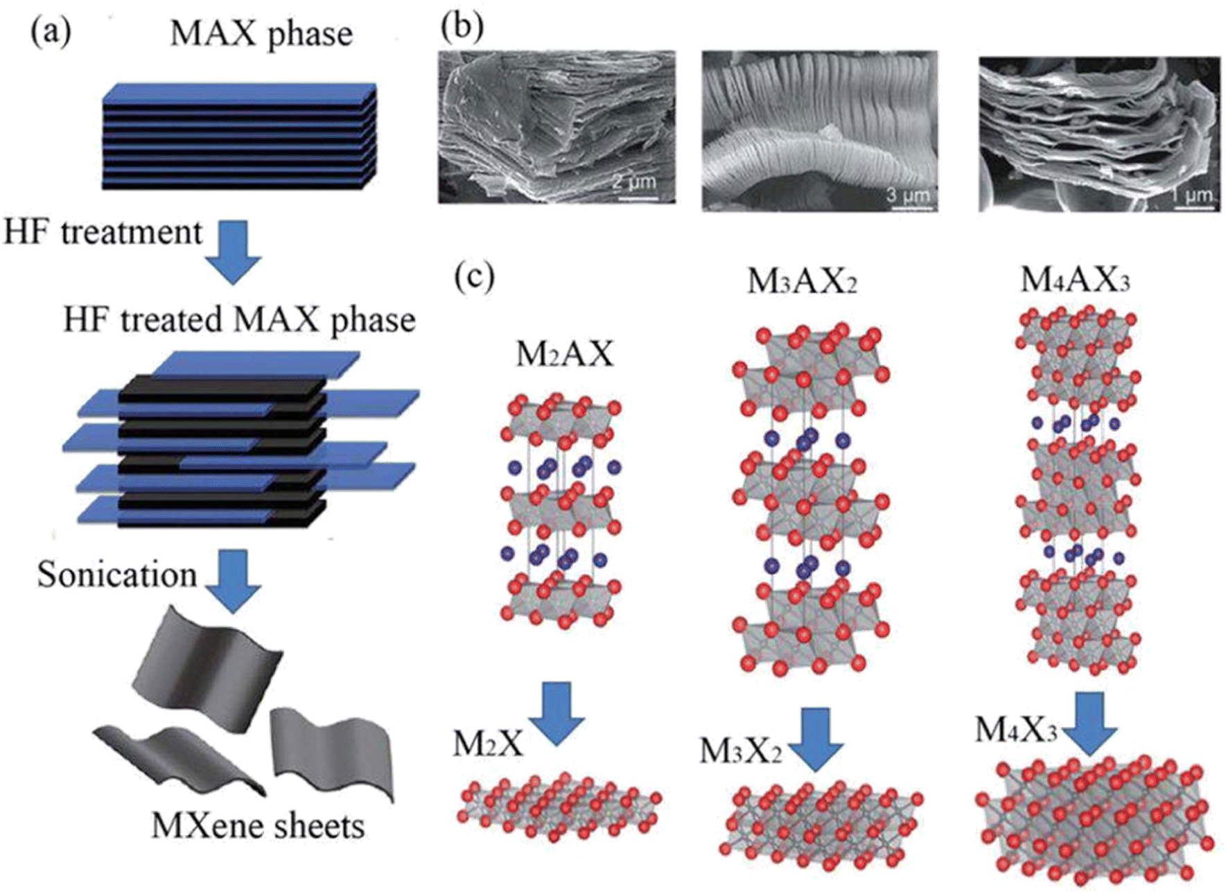 | ||
| Fig. 1 (a) Three distinct MXene (non-terminated) structures were initially reported: M2X, M3X2, and M4X3. (b) SEM pictures of Ti2AlC, Ti3AlC2, and Ti4AlC3 (from right to left) after HF treatment. (c) Illustration of the synthesis of MXenes from MAX phases in a schematic form. | ||
The preparation methods are classified as follows.
Etching methods
| Ti3AlC2 + 3HF = AlF3 + 3/2H2 + Ti3C2 | (1) |
| Ti3C2 + 2H2O = Ti3C2OH2 + H2 | (2) |
| Ti3C2 + 2HF = Ti3C2F2 + H2 | (3) |
The etching time depends also on the M atom. The M atoms with a larger number of valence electrons require stronger etching. For example, Nb2AlC requires three times longer stirring time than Ti3C2Tx.28 Though etching of MXenes with HF produces a high yield, this process is hazardous due to the highly toxic and corrosive nature of HF. So, it is critical to follow safety measures during work with HF. This etching process produces H2 gas as a byproduct; this gas is highly flammable and easily escapes to the surrounding environment.29Fig. 1b shows the SEM images of MXenes after HF treatment and Fig. 1c shows different types of MXene structures.
As the HF is highly corrosive and toxic, some following alternative methods are explored.
(i) Molten fluoride-based etching method: to overcome the above limitation with HF, LiF![[thin space (1/6-em)]](https://www.rsc.org/images/entities/char_2009.gif) :NaF:KF = 29:12:59, weight ratio, a molten fluoride salt was developed by Urbankowski et al. as an etchant.30 This procedure occurs under high temperatures. The etching process can be completed within 30 minutes, which is very effective. As this process needs a high temperature this can be a demerit of this process.
:NaF:KF = 29:12:59, weight ratio, a molten fluoride salt was developed by Urbankowski et al. as an etchant.30 This procedure occurs under high temperatures. The etching process can be completed within 30 minutes, which is very effective. As this process needs a high temperature this can be a demerit of this process.
(ii) LiF/HCl method: as HF is hazardous, a new method is introduced to remove A from MAX, using LiF/HCl as the etchant. Li+ ion continuously intercalates between the MXene layer and thus weakens the bonding between M and A and successively removes the A layer from MXenes.27 This process also produces H2 gas, which is flammable.29
(iii) MS-E-etching process (molten salt assisted electrochemical etching: fluorine-free): the methods discussed above have a harmful influence on the environment. This method can be easily accessible due to adequate lithium and potassium resources in salt-lakes and LiCl–KCl (1:1 wt%) salts at 450 °C. From Fig. 3 we can see that when a potential 2.0 volt is applied, Ti3C2Tx releases electrons from its active sites and the Cl atom absorbs onto this active site, forming a strong AlCl3 bond.31 As the boiling point of AlCl3 is 180 °C it can rapidly evaporate at 450 °C.32 This process is environmentally friendly and the recovered salt after synthesis can be recycled and reused (Fig. 2).33,34
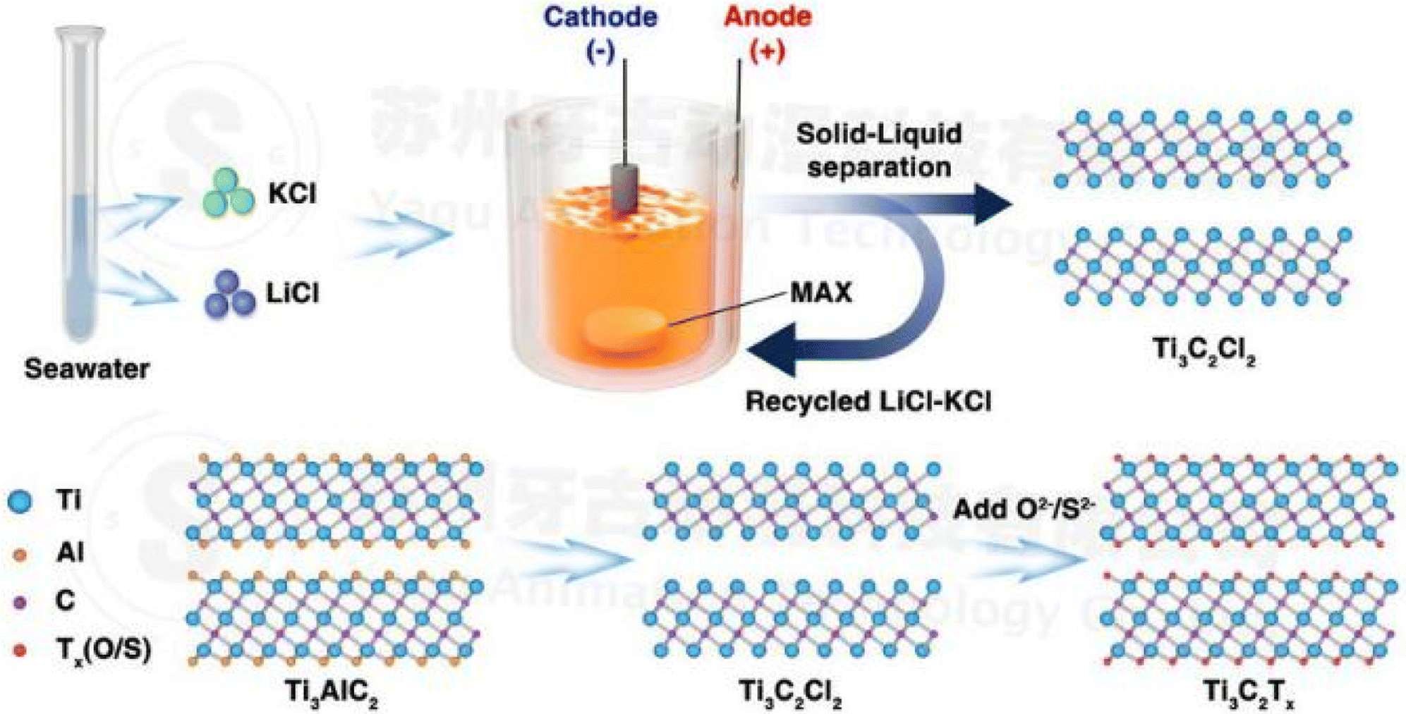 | ||
| Fig. 2 Synthesis of MXenes through MS-E-etching from the MAX phase, followed by the controlled surface terminations facilitated by ample lithium and potassium resources found in salt lakes. Notably, the utilization of eutectic salts comprising LiCl and KCl, characterized by a low melting point, contributes to the controllability of the process (copyright 2021 John Wiley and Sons).32 | ||
Etching methods are relatively simple and widely used. However, this process requires hazardous and toxic chemicals (e.g., HF), and specialized safety precautions, which limit its use in MXene preparation.
Chemical vapor deposition
Alternative approaches to MXene synthesis, including bottom-up methods like chemical vapor deposition (CVD), have shown promising results.35,36 For instance, in 2015, ultrathin 2D α-Mo2C crystals, with thicknesses of only a few nanometers and lateral dimensions of up to 100 micrometers, were successfully produced through CVD. This process involved utilizing methane on a bilayer substrate composed of copper foil placed on a molybdenum foil.35 This CVD technique has also been extended to create ultrathin WC and TaC crystals using other transition metals like W and Ta.35 Notably, this method offers the advantage of generating MXenes with substantial lateral sizes and minimal defects, which greatly facilitates the investigation of their intrinsic properties. While the synthesis of MXene monolayers using this method has yet to be demonstrated, there is still room for further exploration and development of bottom-up synthesis approaches for MXenes. CVD offers precise control over MXene thickness and morphology. However, this process needs sophisticated instruments and skilled operators.Synthesis of functionalized MXenes
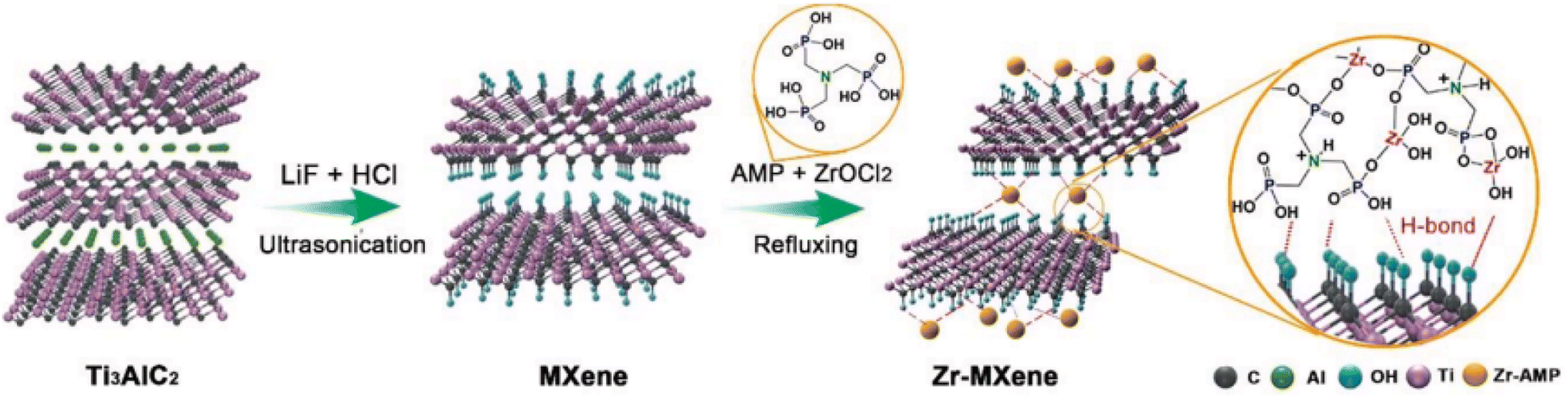 | ||
| Fig. 3 Scheme for the Zr–MXene preparation.37 | ||
Functionalization of MXenes by silylation
There is a need to improve MXenes' stability. Ji et al. demonstrated a straightforward silylation approach (shown in Fig. 4) for successfully stabilizing MXenes against spontaneous oxidation-induced structural breakdown and improving surface properties with variable hydrophilicity.38 The MXene solution was centrifuged at 13000 rpm for about 30 min. The sediment was then collected and dissolved in 95 percent pure ethanol. Hexadecyltrimethoxysilane, 3-aminopropyl triethoxysilane, and 1H,1H,2H,2H-perfluorodecyltriethoxysilane were all reacted with 200 L of MXenes in ethanol (total volume 2 mL) at various concentrations (0, 1, 5, 10, 20, 50, 100, 200, 500, and 1000 L). The samples were then each repeatedly rinsed with water and dissolved in 1 mL of water.
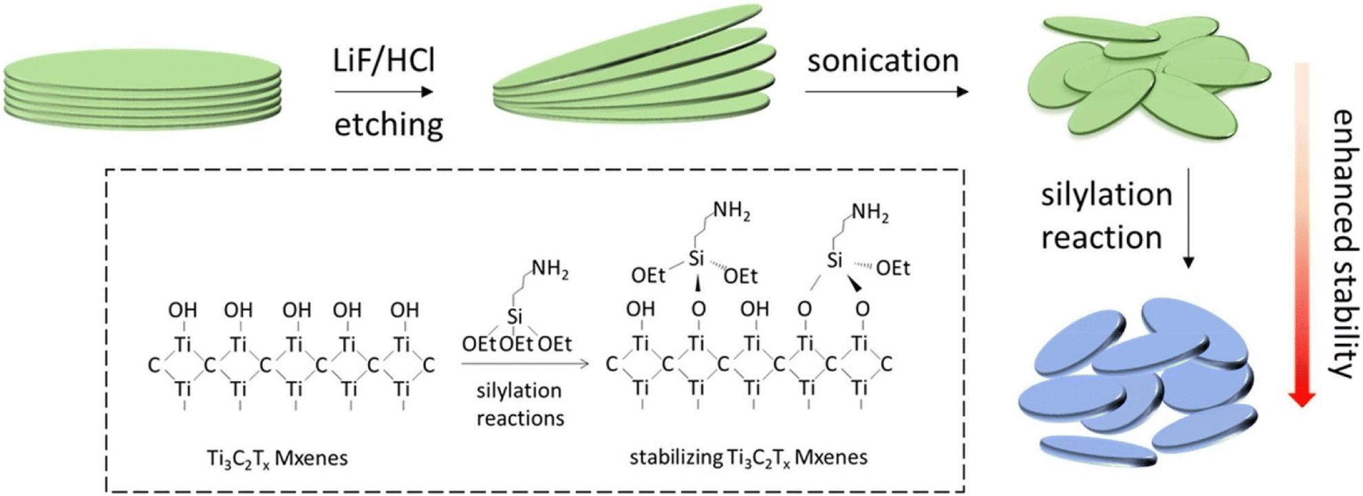 | ||
| Fig. 4 Selective etching and sonication of MXenes with LiF/HCl (copyright 2019 Elsevier). | ||
MXenes can, therefore, be created in a variety of forms, including multilayer powders and inks made of delaminated flakes dissolved in water. These inks can then be printed, sprayed, pulled into fibers, or filtered into freestanding films. The etching technique, the intended application, the needed concentration, and the sonication step all play a significant role. Longer sonication times and stronger sonication forces will result in smaller flakes with more flaws and maybe different concentrations than non-sonicated samples. The technique of synthesis and the kind of intercalants employed to reduce the inter-layer contact between MXene sheets are two additional factors that affect the concentration of MXene sheets in solution. This section details the benefits and drawbacks of processing Ti3C2Tx. Ultrasonic is another method other than etching which reduced the etching time to 4 h to 24 h. In this method Ti3C2Tx was slowly added to an etchant in a beaker, and then the beaker was placed into an ultrasonic homogenizer for 4 h23 As there is a different etching process, different groups can be attached with M atoms and the characteristic of the surface of MXenes highly depends on their preparation method.22
Characterization
Several characterization techniques are commonly employed to analyze MXenes. Visual appearance is an important aspect of MXene characterization, as it provides qualitative information about the morphology, color, and texture of MXene materials. MXenes are a class of two-dimensional materials with unique properties, and their characterization is crucial for understanding their structure, properties, and potential applications. FTIR helps identify functional groups and chemical bonds present in MXenes. It is particularly useful for assessing surface modifications and chemical interactions.41 UV-Vis spectroscopy plays a crucial role in MXene characterization by providing valuable information about their electronic structure, optical properties, concentration, stability, and chemical modifications.42Accurately quantifying the ratio of oxygen groups (![[double bond, length as m-dash]](https://www.rsc.org/images/entities/char_e001.gif) O) to hydroxyl groups (–OH) on MXene surfaces presents a formidable challenge. Similarly, the quantitative analysis of fluorine termination (–F) is problematic due to the formation of fluoride by-products, such as AlF3. The detection of light elements is generally challenging in analytical science because of their low atomic mass and compact electron clouds. Nuclear Magnetic Resonance (NMR) is a technique that probes atomic nuclei when there is a deviation from a spin number of 0. Hydrogen (H) and fluorine (F) are amenable to NMR analysis because they possess an odd number of neutrons. NMR experiments have provided insights into MXene surface chemistry, revealing that there are fewer –OH terminations compared to –F or –O terminations on the surface of Ti3C2Tx. Furthermore, these studies have demonstrated the high sensitivity of surface terminations to the specific synthesis methods employed.
O) to hydroxyl groups (–OH) on MXene surfaces presents a formidable challenge. Similarly, the quantitative analysis of fluorine termination (–F) is problematic due to the formation of fluoride by-products, such as AlF3. The detection of light elements is generally challenging in analytical science because of their low atomic mass and compact electron clouds. Nuclear Magnetic Resonance (NMR) is a technique that probes atomic nuclei when there is a deviation from a spin number of 0. Hydrogen (H) and fluorine (F) are amenable to NMR analysis because they possess an odd number of neutrons. NMR experiments have provided insights into MXene surface chemistry, revealing that there are fewer –OH terminations compared to –F or –O terminations on the surface of Ti3C2Tx. Furthermore, these studies have demonstrated the high sensitivity of surface terminations to the specific synthesis methods employed.
Apart from these several characterization techniques are adopted for the MXene, which are illustrated in this section.
Additionally, two broad peaks between 1000 and 1800 cm−1 were seen in Fig. 5, and these were identified as the D and G peaks of graphitic carbon. The increased laser power, which caused the creation of oxidized Ti3C2, may be to blame for the peak's high intensity at about 151 cm−1. These findings, which are corroborated by several accounts in the literature, indicate that Ti3C2Tx was successfully synthesized. The out-of-plane vibrations of the Ti and C atoms were confirmed by the peak at 208 (denoted by an asterisk *).43
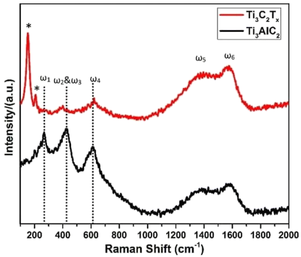 | ||
| Fig. 5 The Raman spectra exhibit distinctive features for both Ti3AlC2 MAX powder and Ti3C2Tx MXene. Peaks labeled with “*” specifically correspond to the out-of-plane vibrations of titanium (Ti) and carbon (C) atoms in the structure. | ||
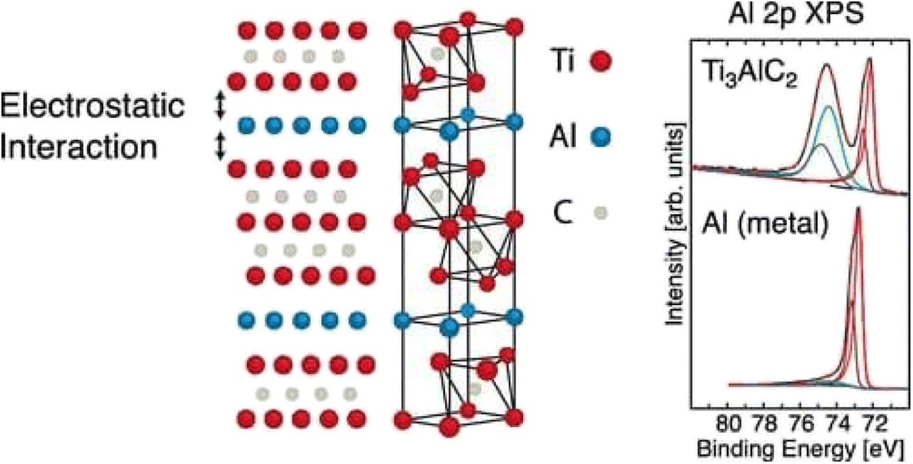 | ||
| Fig. 6 X-ray photoelectron spectroscopy of Ti3AlC2.45 | ||
This X-ray photoelectron spectroscopy data shows us the weak interaction between Ti3C2 layers and Al layers, as shown in Fig. 7. This result confirms us also the selective etching of Al layers in MXenes. The sample was prepared by immersion of DC-MS obtained Ti3C2Tx in 10% concentrated HF (aq.) for 1 h at room temperature and then rinsing with DI water and ethanol.
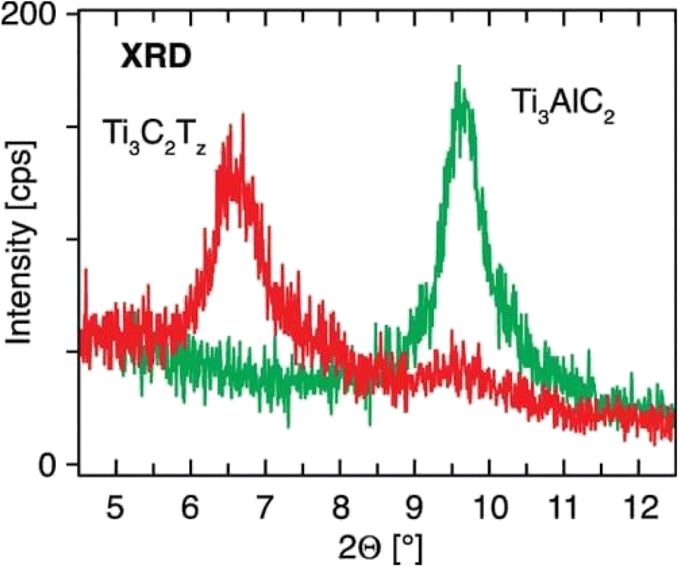 | ||
| Fig. 7 XRD image of Ti3AlC2 and Ti3C2Tx. The diffractogram shows the Ti3AlC2 film at 9.65 and the Ti3C2Tx film at 6.60.45 | ||
Fig. 7 shows the XRD spectrum of Ti3AlC2 film at 9.65 and Ti3C2Tx film at 6.60, respectively. From this we can confirm that the Al layer is etched from MAX successfully.
Electron energy loss spectroscopy (EELS)
XPS typically provides limited spatial resolution. Therefore, when combined with scanning transmission electron microscopy (STEM), electron energy loss spectroscopy (EELS)46 becomes a crucial core-level spectroscopic technique that delivers highly detailed spatial information.47,48 This technique employs a sub-nanometer electron beam probe, ensuring exceptional spatial resolution. As a result, EELS can offer precise chemical bond data on the nanoscale, enabling the characterization of atomic-level bonding environments, such as those found in Ti vacancies and atomic layers within MXene monolayer sheets. In Fig. 8, representative EELS spectra for various edges like C-K, Ti M2,3, F-K, and O-K in MXenes are displayed. These spectra facilitate comparisons between selective etching methods utilizing different etching media, such as HF and LiF/HCl.49 Moreover, EELS opens up opportunities for comprehending chemical reactions at the single-atom level,50 especially when combined with other imaging and spectral techniques like STEM51 and energy dispersive X-ray spectroscopy (EDX).52 This integrated approach enables the identification of Ti adatoms and vacancies within MXene monolayer sheets.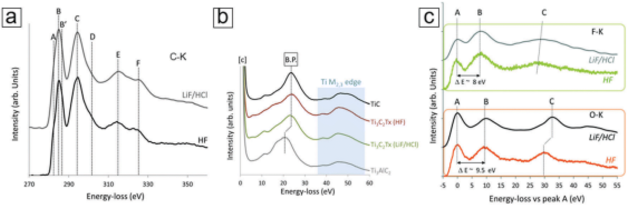 | ||
| Fig. 8 MXene Ti3C2Tx electron energy loss spectroscopy (EELS) curves. (a) C-K edge data of MXenes selectively etched with HF and LiF/HCl. The four major peaks are denoted by the letters C, D, E, and F. (b) The MXenes, TiC, and MAX phases' Ti M2,3 edge peaks. The bulk plasmon (shown as B.P. in the figure panel) shifts as a result of exfoliation. (c) MXenes with distinctive peaks at B: 535 eV and 685 eV, respectively, and F-K and O-K edge peaks. By making the first peak (A) in both spectra zero, they both use relative values (copyright 2018 RSC).53 | ||
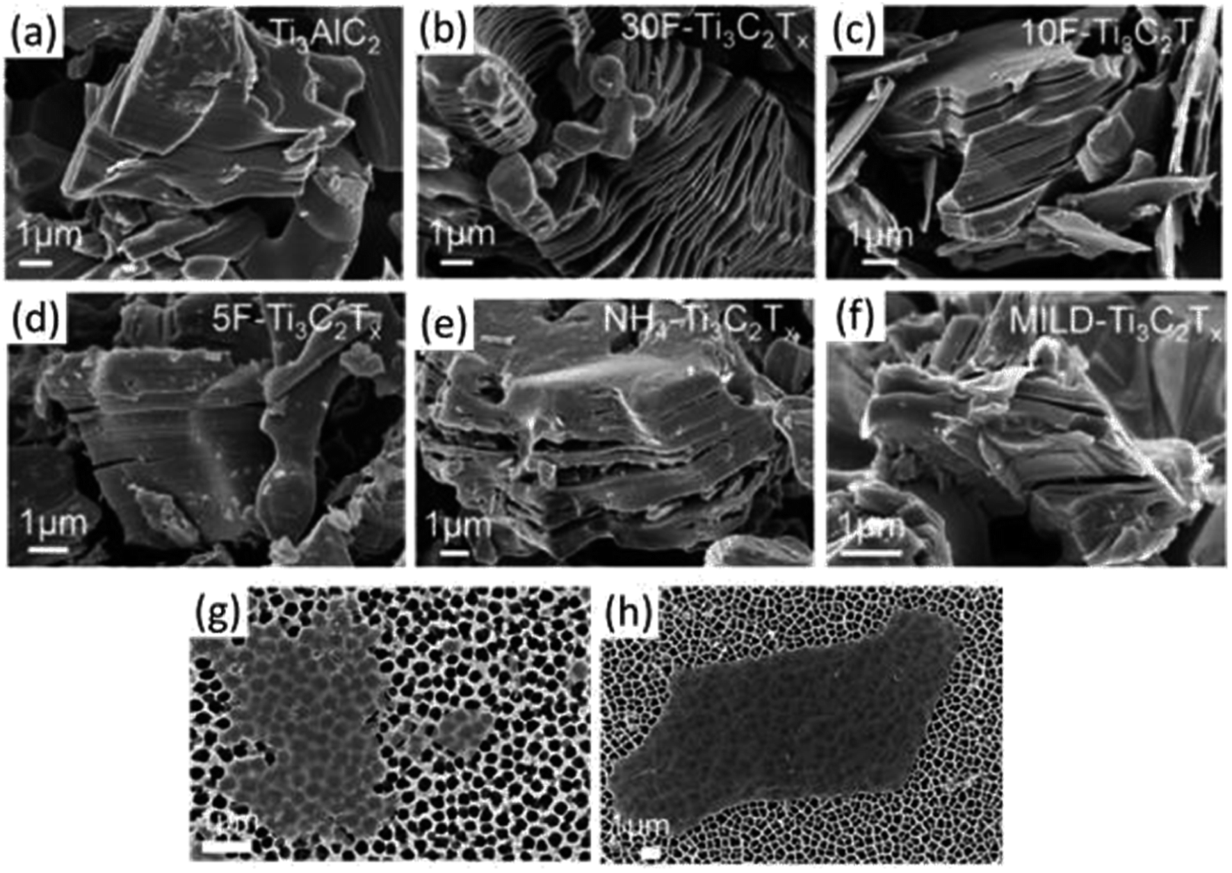 | ||
| Fig. 9 SEM photos of MXenes and MAX powders created by etching under various circumstances. SEM images of (a) Ti3AlC2 (MAX) powder demonstrating the compact layered structure and (b) 30 wt%, (c) 10 wt%, and (d) 5 wt% HF-synthesized multilayered Ti3C2Tx powder. Only after etching in (b) 30 wt% HF (or greater HF concentrations) was an accordion-like morphology seen. (e) Ammonium hydrogen fluoride-synthesized multilayered NH4–Ti3C2Tx powder and (f) the MILD technique (etched with LiF in HCl), both of which exhibit negligible opening of MXene lamellas comparable to that seen in 5F Ti3C2Tx. (g and h) Single MXene flakes on a porous alumina substrate, etched with the 5% HF and MILD methods, are shown in SEM pictures, respectively.1 | ||
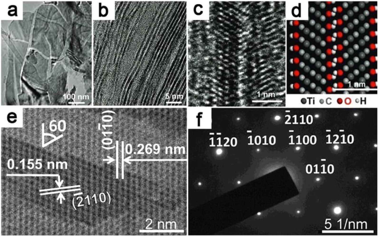 | ||
| Fig. 10 SAED and TEM imaging of MXenes. (a) A TEM picture of exfoliated Ti–C–O–F 2D nanosheets. (b) MXene sheets with one or two layers. (c) HRTEM picture of bilayer Ti3C2(OH)xFy (d) its atomistic model of the layer structure (e) HRTEM image of multilayered MXene and (f) MXene's SAED pattern.54 | ||
Analysis of the surface chemistry of MXenes is a crucial yet difficult undertaking. It is important to keep in mind that each technique has its own limits while investigating the intricate MXene surface chemistry. For instance, high vacuum conditions are used for EELS and XPS studies. This may cause some of the surface species to desorb. In addition, XPS is a surface method with a penetration depth of 10 nm or less. Raman spectroscopy, in contrast, is not only carried out at ambient circumstances but also makes it simple to conduct in situ studies because of the spectrometer's shape. The limited Raman scattering cross-section of metallic materials, however, is known to make them poor Raman scatterers. Additionally, as previously mentioned, MXene peaks are broad, and the spectra can be affected by a variety of circumstances.
Although the majority of the elements (H, C, Al, Si, F, and Li) may be detected via NMR analysis, not all of the components present in MXene samples can be. For NMR investigation,55 the metallic conductivity of MXenes poses new difficulties. Additionally, it's crucial to use water-free samples while performing solid-state NMR on MXenes to prevent signal interference from bulk water. For this reason, annealed samples are used in NMR investigations (200 °C is about right).
Certainly, a comparison chart can provide a concise overview of MXenes in relation to other materials. Below is a simplified comparison chart highlighting the key characteristics of MXenes compared to graphene and traditional semiconductors (e.g., silicon), shown in Table 1. Keep in mind that the actual properties may vary based on specific formulations, synthesis methods, and applications.
| Characteristic | MXene | Graphene | Silicon (Si) |
|---|---|---|---|
| Structure | 2D transition metal carbides/nitrides36 | Single layer of carbon atoms in a hexagonal lattice56 | Crystalline structure with a diamond-like lattice57 |
| Synthesis | Various methods, often involving selective etching27 | Chemical vapor deposition (CVD), liquid-phase exfoliation58 | High-temperature purification from silica59 |
| Conductivity | Good electrical conductivity60 | Excellent electrical conductivity61 | Intrinsic semiconductor with moderate electrical conductivity62–64 |
| Mechanical strength | Generally strong, good mechanical properties65 | Exceptionally strong with high tensile strength66 | Brittle with lower tensile strength compared to carbon materials67 |
| Flexibility | Exhibits flexibility due to its 2D nature68 | Highly flexible and can be bent without breaking69 | Rigid crystalline structure, limited flexibility70 |
| Optical properties | Variable depending on specific MXene formulation71 | Transparent and absorbs only ∼2.3% of light72 | Transparent to infrared and visible light73 |
| Chemical stability | Stable in various chemical environments74 | Stable in most environments75 | Susceptible to oxidation and chemical reactions76 |
| Thermal conductivity | Generally high thermal conductivity77 | High thermal conductivity78 | Moderate thermal conductivity79 |
| Band gap | Tunable band gap (semiconducting behavior)80 | Zero band gap (semimetallic behavior)81 | Intrinsic semiconductor with a fixed band gap82 |
| Applications | Energy storage, catalysis, sensors, electronics83,84 | Flexible electronics, sensors, transparent conductive films85 | Integrated circuits, solar cells, microelectronic86 |
| Environmental impact | Depends on synthesis methods, potential concerns87 | Generally low environmental impact88 | Energy-intensive production, waste concerns89 |
Properties
The exact configuration of surface groups of MXenes depends on their synthesis methods. Actually, MXenes will be modeled with terminating species, which is unrealistic.91 The terminating species that interacted with MXenes with van der Waals or hydrogen bonds should also be taken into account.92
| Properties | Application |
|---|---|
| Electronic | Gas sensors, technical sensors, biosensing, field effect transistor102–109 |
| Magnetic | Spintronics and quantum computing110–113 |
| Mechanical | Mechanical reinforcing material, polymer composites102,114 |
| Optical and photonic | TCO, saturable absorber, mode-locked laser115–119 |
| Electromagnetic | Electromagnetic interference shielding120–122 |
| Thermoelectric | Thermoelectric electricity production123–126 |
| Chemical | Environmental stability, batteries and supercapacitors, other energy storage environmental and water treatment3,127–134 |
| Photothermal | Photothermal therapy135,136 |
Application in the field effect transistor
Different techniques have been used for Hg2+ detection, such as the fluorescence detection technique,137 Atomic Absorption Spectroscopy (AAS),138 Ti3C2Tx-FET,139etc. Among them detection with the MXene-FET took only 10 s and it detects 5 ppm mercury ion rapidly, which is efficient. The Hg2+ absorption energy of MXenes is very high. It is calculated to be −1.298 eV. By compositing a FET with the MXene it can detect Hg2+ rapidly even in a high salinity environment. So, it can be used in real water analysis. It can give a strong response in 1 M NaCl. The sensing capability for Hg2+ in tap water is very feasible; it took only 10 s as mentioned earlier during this detection. When Hg2+ is absorbed in MXenes, Hg2+ is reduced to Hg+ and interacts with the surface terminal group such as Cl, as shown in Fig. 11a.139 The SEM images and output characteristics shown in Fig. 11b and c describe the stability of MXenes after 4 days of storage in air medium. From Fig. 11d we see that the MXene shows n type semiconducting nature. Chengbin Liu et al. provided a Ti3C2Tx MXene FET sensing method for Ag+ detection that exhibits outstanding sensing performance in terms of quick response (a few seconds), simplicity of use, and good sensitivity and selectivity.140
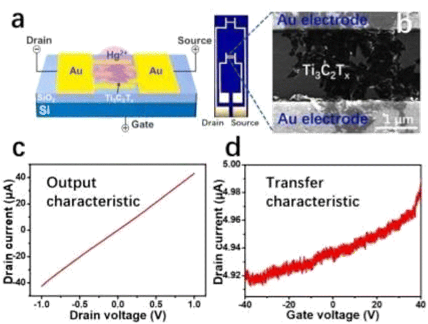 | ||
| Fig. 11 The Ti3C2Tx FET sensor's schematic structure is shown in (a). (b) A picture of the FET sensor electrodes and a SEM image of the Ti3C2Tx nanosheets joining the nearby gold finger electrodes. (c) A Ti3C2Tx FET device's output characteristics and (d) transfer characteristics. | ||
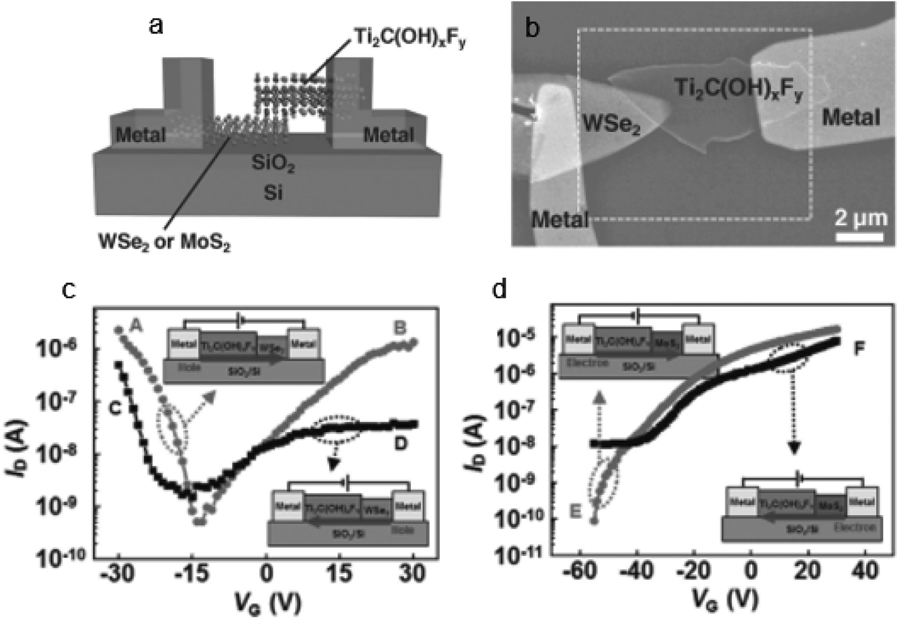 | ||
| Fig. 12 Schematic of a WSe2 (or MoS2)/Ti2C(OH)xFy FET device is shown in (a). (b) Top-view SEM image of a WSe2/Ti2C(OH)xFy FET. The KPFM mapping zone is shown by the rectangle with a dashed border. (c) ID–VG characteristics of the WSe2/Ti2C(OH)xFy FET. For the negative and positive VDS biases, respectively, there are black squares and circles. The insets display schematic illustrations of how the device works. (d) ID–VG properties of the MoS2/Ti2C(OH)xFy FET. The negative and positive VDS biases are shown, respectively, by the black squares and circles (copyright 2016 John Wiley and Sons). | ||
Hanlin Wang et al. showed that the intercalation of Ti3C2Tx with didecyldimethyl ammonium bromide (DDAB), a quaternary ammonium chemical, results in a striking improvement in the charge carrier mobility in ambipolar polymer based OFETs.142 Haihong Xie et al. used an MXene (Ti3C2Tx) as the source electrode and two-dimensional (2D) tin halide perovskite (PEA)2SnI4 as the semiconductor layer to show how metal halide perovskite field-effect transistors are made.143 An ultrathin field-effect transistor made of Ti2CO2 semiconductor and seamlessly connected Ti2CF2 metallic electrodes was considered by Ü. Ö. Akkuş.144
For use in high-performance OFETs, Benzheng Lyu et al. showed how to fabricate a broad, uniform MXene electrode array on a flexible plastic substrate.145 They used asymmetric source and drain electrodes to examine the contact characteristics between the MXene electrodes and the organic semiconductors, as illustrated in Fig. 13a. The transfer curves of the p-type pentacene OFETs with varied electrodes are shown in Fig. 13b. Pentacene was injected with holes when negative VD was supplied to the metal (Au or Al) electrode. Fig. 13b's right panel displays schematic band diagrams of the MXene/pentacene/Au junction at various voltage levels to clarify the carrier injection barrier in each situation.
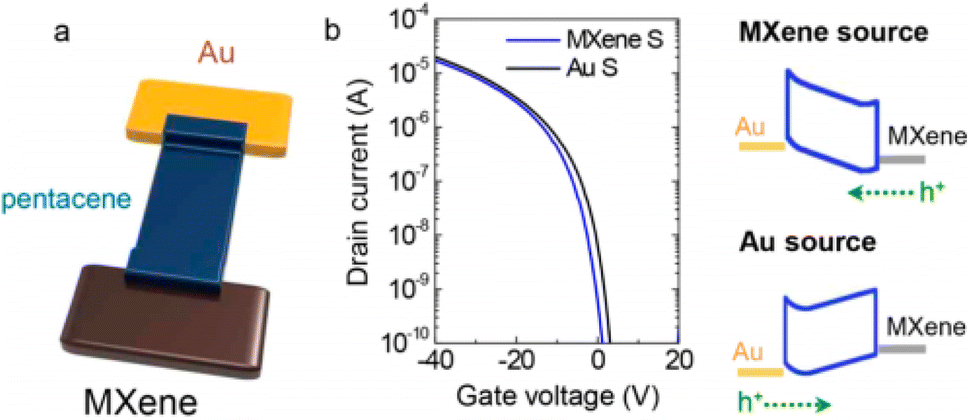 | ||
| Fig. 13 (a) A schematic depiction of MXene/pentacene/Au. (b) P-type pentacene OFET transfer characteristics with a Au source electrode (black) and MXene source electrode (blue) are shown.145 | ||
 | ||
| Fig. 14 FET circuit and illustration of the antibody–antigen sensing mechanism and change in drain source current.17 | ||
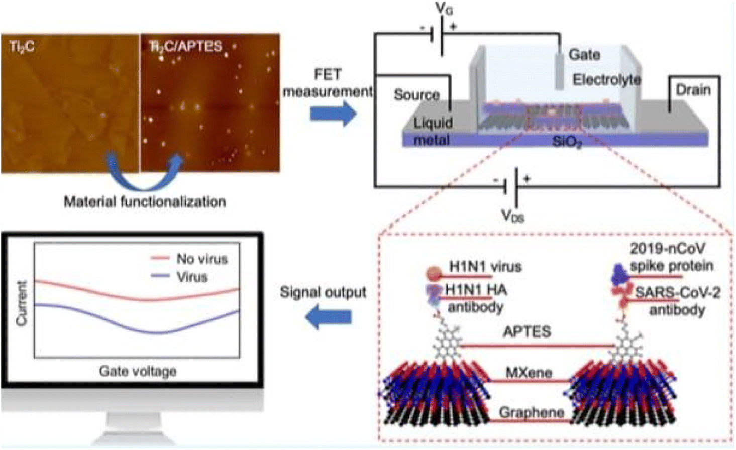
A field-effect transistor (FET)-based biosensing device for detecting SARS-CoV-2 in clinical samples was disclosed by Giwan Seo et al.146 The FET's graphene sheets were coated with an antibody intended to neutralize the SARS-CoV-2 spike protein to develop the sensor. The sensor's performance was evaluated using COVID-19 patients' nasopharyngeal swab samples, cultured virus, and antigen protein (Fig. 15).
 | ||
| Fig. 15 Diagram showing the steps in the COVID-19 FET sensor functioning. The SARS-CoV-2 spike antibody is attached onto the graphene sheet using the interface molecule 1-pyrenebutyric acid N-hydroxysuccinimide ester as a probe linker. Graphene is used as the sensing material.146 | ||
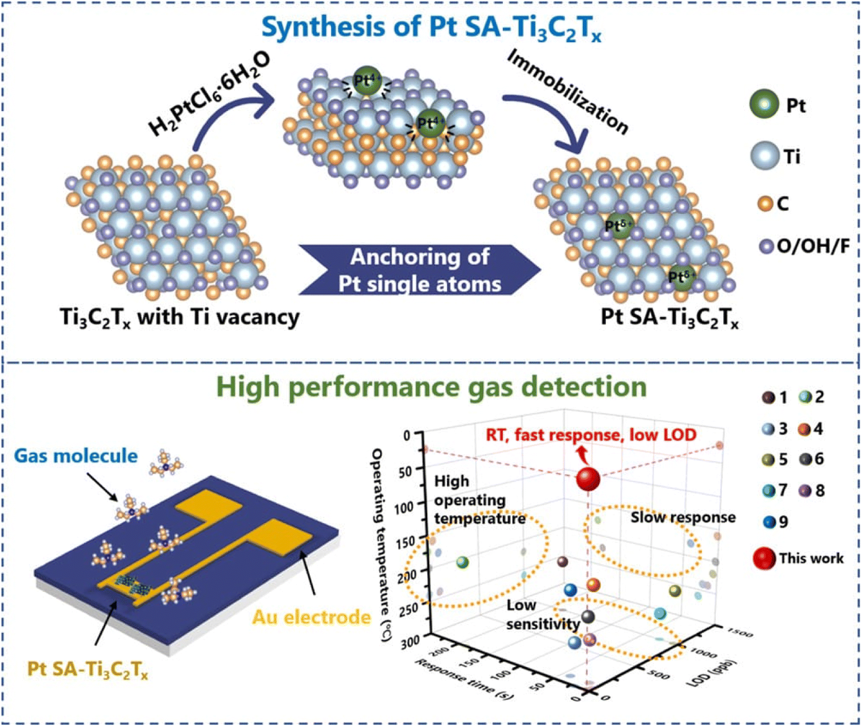 | ||
| Fig. 16 Schematic diagram of the Pt SA–Ti3C2Tx synthesis process and its high detection performance for TEA gas analysis. The Pt SA is synthesized through the immobilization of Pt4+ onto the Ti3C2Tx surface with Ti vacancies. Schematic diagram of the FET sensor device and the detection performance comparison between Pt SA–Ti3C2Tx and other TEA sensors. Data points in the 3D chart are from (1) Pt/SnO2, (2) Ag/WO3, (3) Pt SA/WO3, (4) Fe2O3, (5) WO3/SnO2, (6) Pd/In2O3, (7) Fe/NiO, (8) WO3/Co3O4, and (9) Pt–Ce/In2O3. | ||
Bingzhe Xu et al. created a quick and efficient method for creating FETs based on extremely thin, conductive Ti3C2 MXene micropatterns, which were then used to monitor the spiking activity of hippocampus neurons and perform highly sensitive label-free dopamine detection.151 They used scanning electron microscopy (SEM) to confirm the multilayered structure of the resulting bulk MXenes (Ti3C2Tx) (Fig. 17a). The chemical makeup of the synthesized MXene was further examined using X-ray diffraction (XRD), which revealed the transition from Ti3AlC2 to Ti3C2Tx (Fig. 17b). After etching, the Ti3AlC2 peak at 39° that was the sharpest vanished, suggesting that the Al layer had been removed. Furthermore, the (00l) peaks of Ti3C2Tx like (002) at 9.5° and (004) at 19.4° expanded with less intensity and shifted to lower angles, respectively (8.8° and 18.5°), indicating that Al was substituted by OH or F moieties. Few and single layer MXene flakes are prepared for patterning and sensing applications after being delaminated using sonication and intercalated in dimethyl sulfoxide (DMSO) (Fig. 17c).
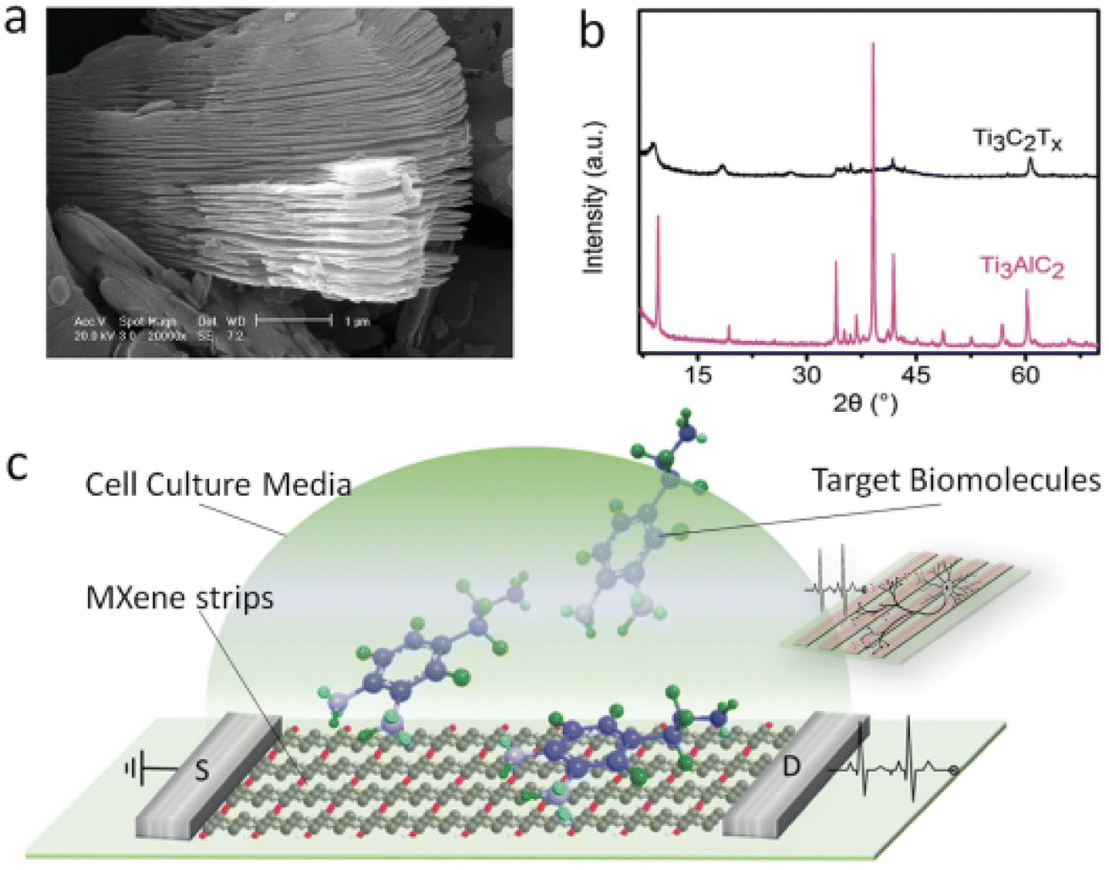 | ||
| Fig. 17 Characterization of bulk MXenes. (a) SEM image of the multilayer structured MXene. (b) XRD patterns of the transition from Ti3AlC2 to Ti3C2Tx. (c) Schematic of a biosensing device based on MXene field effect transistors (copyright 2016 John Wiley and Sons).151 | ||
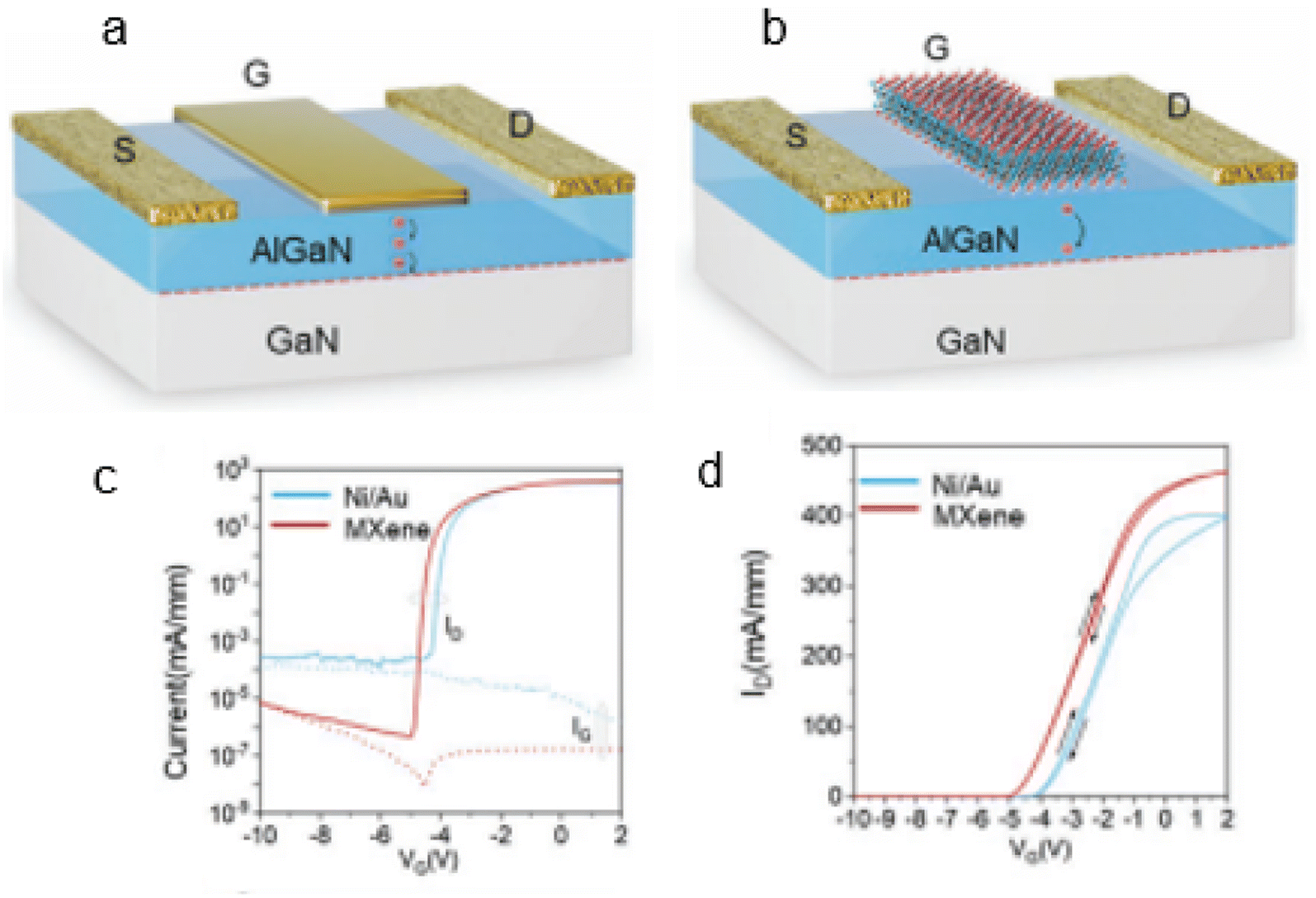 | ||
| Fig. 18 GaN HEMT schematic diagrams with either Ti3C2Tx or (a) Ni/Au or (b) the gate electrodes. (c) The Ni/Au- and MXene-gate GaN HEMTs' IG curves and logarithmic-scale transfer curves. (d) GaN HEMT dual-sweep transfer curves on a linear scale (copyright 2023 John Wiley and Sons). | ||
MXene based FETs have now been used in many other applications like gas sensors,155 electrochemical transistors,156 metal halide perovskite vertical FETs,143 graphene–MXene based materials for diagnosis,157etc.
Addressing these challenges will require collaborative efforts from researchers in materials science, chemistry, and electronics. Overcoming these hurdles will pave the way for the successful integration of MXene-based FETs into practical applications, unlocking the full potential of this promising material in electronic devices.
Conclusion
As we delve deeper into the multifaceted world of MXenes, it becomes increasingly evident that these materials hold the promise of shaping the future of electronic technology. Their unique combination of synthesis versatility, functionalization flexibility, intrinsic properties, and applicability in FETs positions them as a transformative force in the realm of materials science and electronic engineering. This paper will help the researchers to explore the exciting future prospects of MXenes, where their impact on electronic devices is poised to be profound and far-reaching. However, there is still much to be explored in the properties and surface functionalization of MXenes to unlock their full potential. Further work should be needed for optimizing the doping techniques, understanding the doping mechanism for making more active cites that is useful for any detection and enhance the properties of charge transfer method. And also exploring new application in energy storage ability, flexible circuits sensors and comfortable electronics should be investigated. The unique properties and potential applications of MXenes make them an exciting area of research with the potential to revolutionize various fields of science and technology.Author contributions
Maisha Rahman: writings, editing; Muhammad Shamim Al Mamun: conceptualization, supervision, writings, and resources.Conflicts of interest
Authors declare no conflict of interest.Acknowledgements
Authors love to acknowledge Chemistry Discipline, Khulna University for the technical support.References
- Y. Gogotsi and B. Anasori, ACS Nano, 2019, 13, 8491–8494 CrossRef CAS PubMed.
- S. He, X. Sun, H. Zhang, C. Yuan, Y. Wei and J. Li, Macromol. Rapid Commun., 2021, 42, e2100324 CrossRef PubMed.
- J. Nan, X. Guo, J. Xiao, X. Li, W. Chen, W. Wu, H. Liu, Y. Wang, M. Wu and G. Wang, Small, 2021, 17, e1902085 CrossRef.
- R. M. Ronchi, J. T. Arantes and S. F. Santos, Ceram. Int., 2019, 45, 18167–18188 CrossRef CAS.
- Q. Zhu, J. Li, P. Simon and B. Xu, Energy Storage Mater., 2021, 35, 630–660 CrossRef.
- V. Q. Hieu, T. C. Lam, A. Khan, T.-T. Thi Vo, T.-Q. Nguyen, V. D. Doan, D. L. Tran, V. T. Le and V. A. Tran, Chemosphere, 2021, 285, 131429 CrossRef CAS PubMed.
- H. Riazi, M. Anayee, K. Hantanasirisakul, A. A. Shamsabadi, B. Anasori, Y. Gogotsi and M. Soroush, Adv. Mater. Interfaces, 2020, 7, 1902008 CrossRef CAS.
- K. S. Ranjith, A. T. Ezhil Vilian, S. M. Ghoreishian, R. Umapathi, S.-K. Hwang, C. W. Oh, Y. S. Huh and Y.-K. Han, J. Hazard. Mater., 2022, 421, 126775 CrossRef CAS PubMed.
- M. Naguib, O. Mashtalir, J. Carle, V. Presser, J. Lu, L. Hultman, Y. Gogotsi and M. W. Barsoum, ACS Nano, 2012, 6, 1322–1331 CrossRef CAS PubMed.
- M. Mozafari and M. Soroush, Mater. Adv., 2021, 2, 7277–7307 RSC.
- M. Naguib, V. N. Mochalin, M. W. Barsoum and Y. Gogotsi, Adv. Mater., 2014, 26, 992–1005 CrossRef CAS PubMed.
- M. W. Barsoum, in MAX Phases, 2013, pp. 187–235, DOI:10.1002/9783527654581.ch6.
- M. Naguib, M. Kurtoglu, V. Presser, J. Lu, J. Niu, M. Heon, L. Hultman, Y. Gogotsi and M. W. Barsoum, Adv. Mater., 2011, 23, 4248–4253 CrossRef CAS PubMed.
- M. Magnuson, J. Halim and L.-Å. Näslund, J. Electron Spectrosc. Relat. Phenom., 2018, 224, 27–32 CrossRef CAS.
- E. N. Hoffman, G. Yushin, T. El-Raghy, Y. Gogotsi and M. W. Barsoum, Microporous Mesoporous Mater., 2008, 112, 526–532 CrossRef CAS.
- V. T. Le, Y. Vasseghian, V. D. Doan, T. T. T. Nguyen, T.-T. Thi Vo, H. H. Do, K. B. Vu, Q. H. Vu, T. Dai Lam and V. A. Tran, Chemosphere, 2022, 291, 133025 CrossRef CAS.
- Y. Li, Z. Peng, N. J. Holl, M. R. Hassan, J. M. Pappas, C. Wei, O. H. Izadi, Y. Wang, X. Dong, C. Wang, Y.-W. Huang, D. Kim and C. Wu, ACS Omega, 2021, 6, 6643–6653 CrossRef CAS.
- X. Li, G. Fan and C. Zeng, Int. J. Hydrogen Energy, 2014, 39, 14927–14934 CrossRef CAS.
- B. Hammer and J. K. Nørskov, in Advances in Catalysis, Academic Press, 2000, vol. 45, pp. 71–129 Search PubMed.
- Y. Zhang, L. Wang, N. Zhang and Z. Zhou, RSC Adv., 2018, 8, 19895–19905 RSC.
- N. Chen, W. Yang and C. J. Zhang, Sci. Technol. Adv. Mater., 2021, 22, 917–930 CrossRef.
- Z. Wang, IOP Conf. Ser. Earth Environ. Sci., 2021, 714, 042030 CrossRef.
- W. Feng, H. Luo, Y. Wang, S. Zeng, Y. Tan, H. Zhang and S. Peng, Ceram. Int., 2018, 44, 7084–7087 CrossRef CAS.
- U. U. Rahman, M. Humayun, U. Ghani, M. Usman, H. Ullah, A. Khan, N. M. El-Metwaly and A. Khan, Molecules, 2022, 27(15), 4909–4944 CrossRef CAS PubMed.
- L. Wang, M. Zhang, B. Yang, J. Tan, X. Ding and W. Li, Small Methods, 2021, 5, 2100409 CrossRef CAS PubMed.
- K. R. G. Lim, M. Shekhirev, B. C. Wyatt, B. Anasori, Y. Gogotsi and Z. W. Seh, Nat. Synth., 2022, 1, 601–614 CrossRef.
- Y.-J. Kim, S. J. Kim, D. Seo, Y. Chae, M. Anayee, Y. Lee, Y. Gogotsi, C. W. Ahn and H.-T. Jung, Chem. Mater., 2021, 33, 6346–6355 CrossRef CAS.
- L. Gao, C. Li, W. Huang, S. Mei, H. Lin, Q. Ou, Y. Zhang, J. Guo, F. Zhang, S. Xu and H. Zhang, Chem. Mater., 2020, 32, 1703–1747 CrossRef CAS.
- P. Lakhe, E. M. Prehn, T. Habib, J. L. Lutkenhaus, M. Radovic, M. S. Mannan and M. J. Green, Ind. Eng. Chem. Res., 2019, 58, 1570–1579 CrossRef CAS.
- P. Urbankowski, B. Anasori, T. Makaryan, D. Er, S. Kota, P. L. Walsh, M. Zhao, V. B. Shenoy, M. W. Barsoum and Y. Gogotsi, Nanoscale, 2016, 8, 11385–11391 RSC.
- R. S. Alwitt, H. Uchi, T. R. Beck and R. C. Alkire, Electrochemical Society Extended Abstracts, 1982, vol. 82-2, pp. 108–109 Search PubMed.
- M. Shen, W. Jiang, K. Liang, S. Zhao, R. Tang, L. Zhang and J. Q. Wang, Angew Chem. Int. Ed. Engl., 2021, 60, 27013–27018 CrossRef CAS.
- X. Xiao, H. Song, S. Lin, Y. Zhou, X. Zhan, Z. Hu, Q. Zhang, J. Sun, B. Yang, T. Li, L. Jiao, J. Zhou, J. Tang and Y. Gogotsi, Nat. Commun., 2016, 7, 11296 CrossRef CAS PubMed.
- W. Weng, B. Jiang, Z. Wang and W. Xiao, Sci. Adv., 2020, 6, eaay9278 CrossRef CAS PubMed.
- C. Xu, L. Wang, Z. Liu, L. Chen, J. Guo, N. Kang, X.-L. Ma, H.-M. Cheng and W. Ren, Nat. Mater., 2015, 14, 1135–1141 CrossRef CAS PubMed.
- Y. Gogotsi, Nat. Mater., 2015, 14, 1079–1080 CrossRef CAS PubMed.
- L. Liu, M. Zhu, Y. Shi, X. Xu, Z. Ma, B. Yu, S. Fu, G. Huang, H. Wang and P. Song, Chem. Eng. J., 2021, 424, 130338 CrossRef CAS.
- J. Ji, L. Zhao, Y. Shen, S. Liu and Y. Zhang, FlatChem, 2019, 17, 100128 CrossRef CAS.
- L. Yin, C. Liu, C. Ding, C. Zhao, I. Z. Mitrovic, E. G. Lim, H. Wang, Y. Sun, Y. Han, Z. Li, L. Yang, C.-Q. Ma and C. Zhao, Cell Rep. Phys. Sci., 2022, 3, 100905 CrossRef CAS.
- A. S. R. Bati, A. A. Sutanto, M. Hao, M. Batmunkh, Y. Yamauchi, L. Wang, Y. Wang, M. K. Nazeeruddin and J. G. Shapter, Cell Rep. Phys. Sci., 2021, 2, 100598 CrossRef CAS.
- M. Mahmood, A. Rasheed, I. Ayman, T. Rasheed, S. Munir, S. Ajmal, P. O. Agboola, M. F. Warsi and M. Shahid, Energy Fuels, 2021, 35, 3469–3478 CrossRef CAS.
- E. Satheeshkumar, T. Makaryan, A. Melikyan, H. Minassian, Y. Gogotsi and M. Yoshimura, Sci. Rep., 2016, 6, 32049 CrossRef CAS PubMed.
- A. Iqbal and N. M. Hamdan, Materials, 2021, 14, 6292–6310 CrossRef CAS PubMed.
- Y. C. Zhou, X. H. Wang, Z. M. Sun and S. Q. Chen, J. Mater. Chem., 2001, 11, 2335–2339 RSC.
- L.-Å. Näslund, P. O. Å. Persson and J. Rosen, J. Phys. Chem. C, 2020, 124, 27732–27742 CrossRef.
- C. Wiktor, M. Meledina, S. Turner, O. I. Lebedev and R. A. Fischer, J. Mater. Chem. A, 2017, 5, 14969–14989 RSC.
- S. Carenco, S. Moldovan, L. Roiban, I. Florea, D. Portehault, K. Vallé, P. Belleville, C. Boissière, L. Rozes, N. Mézailles, M. Drillon, C. Sanchez and O. Ersen, Nanoscale, 2016, 8, 1260–1279 RSC.
- R. Pal, A. K. Sikder, K. Saito, A. M. Funston and J. R. Bellare, Polym. Chem., 2017, 8, 6927–6937 RSC.
- D. Magne, V. Mauchamp, S. Célérier, P. Chartier and T. Cabioc'h, Phys. Chem. Chem. Phys., 2016, 18, 30946–30953 RSC.
- J. R. Jinschek, Chem. Commun., 2014, 50, 2696–2706 RSC.
- J. C. Yang, M. W. Small, R. V. Grieshaber and R. G. Nuzzo, Chem. Soc. Rev., 2012, 41, 8179–8194 RSC.
- L. Zhao, H. Q. Ta, A. Dianat, A. Soni, A. Fediai, W. Yin, T. Gemming, B. Trzebicka, G. Cuniberti, Z. Liu, A. Bachmatiuk and M. H. Rummeli, Nano Lett., 2017, 17, 4725–4732 CrossRef CAS.
- J. Pang, R. G. Mendes, A. Bachmatiuk, L. Zhao, H. Q. Ta, T. Gemming, H. Liu, Z. Liu and M. H. Rummeli, Chem. Soc. Rev., 2019, 48, 72–133 RSC.
- H. Alnoor, A. Elsukova, J. Palisaitis, I. Persson, E. N. Tseng, J. Lu, L. Hultman and P. O. Å. Persson, Mater. Today Adv., 2021, 9, 100123–100138 CrossRef CAS.
- T. Kobayashi, Y. Sun, K. Prenger, D.-e. Jiang, M. Naguib and M. Pruski, J. Phys. Chem. C, 2020, 124, 13649–13655 CrossRef CAS.
- G. Yang, L. Li, W. B. Lee and M. C. Ng, Sci. Technol. Adv. Mater., 2018, 19, 613–648 CrossRef CAS PubMed.
- T. A. Khachaturova, V. G. But'ko and A. A. Gusev, JETP Lett., 2022, 115, 41–44 CrossRef CAS.
- M. Saeed, Y. Alshammari, S. A. Majeed and E. Al-Nasrallah, Molecules, 2020, 25, 3856–3918 CrossRef CAS.
- A. Daulay, M. Andriayani and S. Gea, Case Stud. Chem. Environ. Eng., 2022, 6, 100256 CrossRef CAS.
- N. Zhang, Y. Hong, S. Yazdanparast and M. Asle Zaeem, 2D Mater., 2018, 5, 045004 CrossRef CAS.
- L. Chen, N. Li, X. Yu, S. Zhang, C. Liu, Y. Song, Z. Li, S. Han, W. Wang, P. Yang, N. Hong, S. Ali and Z. Wang, Chem. Eng. J., 2023, 462, 142139 CrossRef CAS.
- M. L. Schultz, Infrared Phys., 1964, 4, 93–112 CrossRef CAS.
- K. Huang, Q. Wang, X. Yan, M. Yu, X. Shen, L. Chen and J. Chen, Opt. Commun., 2014, 320, 169–172 CrossRef CAS.
- B. O. Kolbesen and A. Mühlbauer, Solid-State Electron., 1982, 25, 759–775 CrossRef CAS.
- S. Tian, K. Zhou, C.-Q. Huang, C. Qian, Z. Gao and Y. Liu, Extreme Mech. Lett., 2022, 57, 101921 CrossRef.
- D. G. Papageorgiou, I. A. Kinloch and R. J. Young, Prog. Mater. Sci., 2017, 90, 75–127 CrossRef CAS.
- M. Ganchenkova and R. M. Nieminen, in Handbook of Silicon Based MEMS Materials and Technologies, ed. M. Tilli, T. Motooka, V.-M. Airaksinen, S. Franssila, M. Paulasto-Kröckel and V. Lindroos, William Andrew Publishing, Boston, 2nd edn, 2015, pp. 253–293, DOI:10.1016/B978-0-323-29965-7.00009-9.
- Y. Guan, R. Zhao, Y. Cong, K. Chen, J. Wu, H. Zhu, Z. Dong, Q. Zhang, G. Yuan, Y. Li, J. Zhang and X. Li, Chem. Eng. J., 2022, 433, 133582 CrossRef CAS.
- U. Stöberl, U. Wurstbauer, W. Wegscheider, D. Weiss and J. Eroms, Appl. Phys. Lett., 2008, 93, 051906–051909 CrossRef.
- L. Feng, W. Wang, B. Song, X. Zhu, L. Wang, R. Shao, T. Li, X. Pei, L. Wang, X. Qian and Z. Xu, Prog. Org. Coat., 2023, 174, 107286 CrossRef CAS.
- X. Gao, Z. Jia, B. Wang, X. Wu, T. Sun, X. Liu, Q. Chi and G. Wu, Chem. Eng. J., 2021, 419, 130019 CrossRef CAS.
- E. D. Obraztsova, M. G. Rybin and P. A. Obraztsov, in Graphene, ed. V. Skakalova and A. B. Kaiser, Woodhead Publishing, 2nd edn, 2021, pp. 133–142, DOI:10.1016/B978-0-08-102848-3.00006-2.
- M. A. Green and M. J. Keevers, Prog. Photovolt.: Res. Appl., 1995, 3, 189–192 CrossRef CAS.
- S. Athavale, S. Micci-Barreca, K. Arole, V. Kotasthane, J. Blivin, H. Cao, J. L. Lutkenhaus, M. Radovic and M. J. Green, Langmuir, 2023, 39, 918–928 CrossRef CAS.
- S. Lin, J. Tang, K. Zhang, Y. Chen, R. Gao, H. Yin and L.-C. Qin, Nanoscale Adv., 2023, 5, 1163–1171 RSC.
- L. Duan, D. Walter, N. Chang, J. Bullock, D. Kang, S. P. Phang, K. Weber, T. White, D. Macdonald, K. Catchpole and H. Shen, Nat. Rev. Mater., 2023, 8, 261–281 CrossRef CAS.
- C. I. Idumah, Polym.-Plast. Technol. Mater., 2023, 62, 510–546 CAS.
- D. Kumar Das, H. Bhattacharjee, S. Kumar Sahoo and S. Sahoo, Mater. Today: Proc., 2023 DOI:10.1016/j.matpr.2023.06.149.
- C. Cui, Y. Zhang, T. Ouyang, M. Chen, C. Tang, Q. Chen, C. He, J. Li and J. Zhong, Phys. Rev. Mater., 2023, 7, 033803 CrossRef CAS.
- C. Hu, Z. Du, Z. Wei, L. Li and G. Shen, Appl. Phys. Rev., 2023, 10, 021402–021410 CAS.
- A. M. Rojas-Cuervo and R. R. Rey-González, Chem. Phys., 2023, 565, 111744 CrossRef CAS.
- P. Saha, S. Majety and M. Radulaski, Sci. Rep., 2023, 13, 4112 CrossRef CAS.
- S. Nahirniak, A. Ray and B. Saruhan, Batteries, 2023, 9, 126 CrossRef CAS.
- Q. Wang, N. Han, Z. Shen, X. Li, Z. Chen, Y. Cao, W. Si, F. Wang, B.-J. Ni and V. K. Thakur, Nano Mater. Sci., 2023, 5, 39–52 CrossRef CAS.
- H. Lin, Q. Jian, X. Bai, D. Li, Z. Huang, W. Huang, S. Feng and Z. Cheng, Appl. Therm. Eng., 2023, 218, 119176 CrossRef CAS.
- S. P. Muduli and P. Kale, Mater. Sci. Semicond. Process., 2023, 154, 107202 CrossRef CAS.
- N. H. Solangi, R. R. Karri, S. A. Mazari, N. M. Mubarak, A. S. Jatoi, G. Malafaia and A. K. Azad, Coord. Chem. Rev., 2023, 477, 214965 CrossRef CAS.
- V. Manikandan and N. Y. Lee, Chemosphere, 2023, 311, 136934 CrossRef CAS.
- H. Liang and F. You, Nat. Commun., 2023, 14, 1274 CrossRef CAS.
- X. Xie, S. Chen, W. Ding, Y. Nie and Z. Wei, Chem. Commun., 2013, 49, 10112–10114 RSC.
- J.-C. Lei, X. Zhang and Z. Zhou, Front. Phys., 2015, 10, 276–286 CrossRef.
- X. Wang, X. Shen, Y. Gao, Z. Wang, R. Yu and L. Chen, J. Am. Chem. Soc., 2015, 137, 2715–2721 CrossRef CAS.
- M. Kurtoglu, M. Naguib, Y. Gogotsi and M. W. Barsoum, MRS Commun., 2012, 2, 133–137 CrossRef CAS.
- H. Lashgari, M. R. Abolhassani, A. Boochani, S. M. Elahi and J. Khodadadi, Solid State Commun., 2014, 195, 61–69 CrossRef CAS.
- M. Khazaei, M. Arai, T. Sasaki, C.-Y. Chung, N. S. Venkataramanan, M. Estili, Y. Sakka and Y. Kawazoe, Adv. Funct. Mater., 2013, 23, 2185–2192 CrossRef CAS.
- C. Si, J. Zhou and Z. Sun, ACS Appl. Mater. Interfaces, 2015, 7, 17510–17515 CrossRef CAS.
- G. Gao, G. Ding, J. Li, K. Yao, M. Wu and M. Qian, Nanoscale, 2016, 8, 8986–8994 RSC.
- G. Wang, J. Phys. Chem. C, 2016, 120, 18850–18857 CrossRef CAS.
- W. Sun, Y. Xie and P. R. C. Kent, Nanoscale, 2018, 10, 11962–11968 RSC.
- Y. Yuan, D. Cao, Y. Zhang, J. Ma, J. Qi, Q. Wang, G. Lu, Y. Wu, J. Yan, Y. Shi, X. Zhang and G. F. Gao, Nat. Commun., 2017, 8, 15092 CrossRef CAS PubMed.
- K. Rasool, R. P. Pandey, P. A. Rasheed, S. Buczek, Y. Gogotsi and K. A. Mahmoud, Mater. Today, 2019, 30, 80–102 CrossRef CAS.
- J. L. Hart, K. Hantanasirisakul, A. C. Lang, B. Anasori, D. Pinto, Y. Pivak, J. T. van Omme, S. J. May, Y. Gogotsi and M. L. Taheri, Nat. Commun., 2019, 10, 522 CrossRef CAS PubMed.
- R. Ibragimova, P. Erhart, P. Rinke and H. P. Komsa, J. Phys. Chem. Lett., 2021, 12, 2377–2384 CrossRef CAS PubMed.
- R. Bhardwaj and A. Hazra, J. Mater. Chem. C, 2021, 9, 15735–15754 RSC.
- S. J. Kim, H.-J. Koh, C. E. Ren, O. Kwon, K. Maleski, S.-Y. Cho, B. Anasori, C.-K. Kim, Y.-K. Choi, J. Kim, Y. Gogotsi and H.-T. Jung, ACS Nano, 2018, 12, 986–993 CrossRef CAS PubMed.
- J. Choi, Y.-J. Kim, S.-Y. Cho, K. Park, H. Kang, S. J. Kim and H.-T. Jung, Adv. Funct. Mater., 2020, 30, 2003998 CrossRef CAS.
- Y.-W. Cai, X.-N. Zhang, G.-G. Wang, G.-Z. Li, D.-Q. Zhao, N. Sun, F. Li, H.-Y. Zhang, J.-C. Han and Y. Yang, Nano Energy, 2021, 81, 105663 CrossRef CAS.
- K. Chang, M. Guo, L. Pu, J. Dong, L. Li, P. Ma, Y. Huang and T. Liu, Chem. Eng. J., 2023, 451, 138578 CrossRef CAS.
- Y. Wang, Y. Yue, F. Cheng, Y. Cheng, B. Ge, N. Liu and Y. Gao, ACS Nano, 2022, 16, 1734–1758 CrossRef CAS PubMed.
- Q. Song, F. Ye, L. Kong, Q. Shen, L. Han, L. Feng, G. Yu, Y. Pan and H. Li, Adv. Funct. Mater., 2020, 30, 2000475 CrossRef CAS.
- L. Gao, W. Bao, A. V. Kuklin, S. Mei, H. Zhang and H. Ågren, Adv. Mater., 2021, 33, e2004129 CrossRef PubMed.
- E. M. D. Siriwardane, P. Karki, Y. L. Loh and D. Çakır, J. Phys. Chem. C, 2019, 123, 12451–12459 CrossRef CAS.
- Y. Zhang, B. Sa, N. Miao, J. Zhou and Z. Sun, J. Mater. Chem. A, 2021, 9, 10882–10892 RSC.
- R. Thankappan, K. G. Vasanthakumari and U. M. Uzma Sulthana, J. Mater. Sci.: Mater. Electron., 2022, 33, 24542–24549 CrossRef CAS.
- G. R. Berdiyorov, AIP Adv., 2016, 6, 055105–055112 CrossRef.
- A. Di Vito, A. Pecchia, M. Auf der Maur and A. Di Carlo, Adv. Funct. Mater., 2020, 30, 1909028 CrossRef CAS.
- Y. I. Jhon, J. Koo, B. Anasori, M. Seo, J. H. Lee, Y. Gogotsi and Y. M. Jhon, Adv. Mater., 2017, 29, 1702496 CrossRef.
- W. Shui, J. Li, H. Wang, Y. Xing, Y. Li, Q. Yang, X. Xiao, Q. Wen and H. Zhang, Adv. Opt. Mater., 2020, 8, 2001120 CrossRef CAS.
- L. Gao, C. Ma, S. Wei, A. V. Kuklin, H. Zhang and H. Ågren, ACS Nano, 2021, 15, 954–965 CrossRef CAS.
- J. Liu, H. B. Zhang, R. Sun, Y. Liu, Z. Liu, A. Zhou and Z. Z. Yu, Adv. Mater., 2017, 29, 1702367–1702372 CrossRef PubMed.
- M.-S. Cao, Y.-Z. Cai, P. He, J.-C. Shu, W.-Q. Cao and J. Yuan, Chem. Eng. J., 2019, 359, 1265–1302 CrossRef CAS.
- Q.-W. Wang, H.-B. Zhang, J. Liu, S. Zhao, X. Xie, L. Liu, R. Yang, N. Koratkar and Z.-Z. Yu, Adv. Funct. Mater., 2019, 29, 1806819 CrossRef.
- H. Kim, B. Anasori, Y. Gogotsi and H. N. Alshareef, Chem. Mater., 2017, 29, 6472–6479 CrossRef CAS.
- S. Sarikurt, D. Çakır, M. Keçeli and C. Sevik, Nanoscale, 2018, 10, 8859–8868 RSC.
- X. Lu, Q. Zhang, J. Liao, H. Chen, Y. Fan, J. Xing, S. Gu, J. Huang, J. Ma, J. Wang, L. Wang and W. Jiang, Adv. Energy Mater., 2020, 10, 1902986 CrossRef CAS.
- W. Ding, P. Liu, Z. Bai, Y. Wang, G. Liu, Q. Jiang, F. Jiang, P. Liu, C. Liu and J. Xu, Adv. Mater. Interfaces, 2020, 7, 2001340 CrossRef CAS.
- J. Ma, Q. Jiang, Y. Zhou, W. Chu, S. Perathoner, C. Jiang, K. H. Wu, G. Centi and Y. Liu, Small, 2021, 17, e2007509 CrossRef PubMed.
- X. Li, Z. Huang, C. E. Shuck, G. Liang, Y. Gogotsi and C. Zhi, Nat. Rev. Chem, 2022, 6, 389–404 CrossRef PubMed.
- Y. Wei, L. Xiang, H. Ou, F. Li, Y. Zhang, Y. Qian, L. Hao, J. Diao, M. Zhang, P. Zhu, Y. Liu, Y. Kuang and G. Chen, Adv. Funct. Mater., 2020, 30, 2005135 CrossRef CAS.
- H. Chen, Y. Wen, Y. Qi, Q. Zhao, L. Qu and C. Li, Adv. Funct. Mater., 2020, 30, 1906996 CrossRef CAS.
- J. Yang, W. Bao, P. Jaumaux, S. Zhang, C. Wang and G. Wang, Adv. Mater. Interfaces, 2019, 6, 1802004 CrossRef.
- K. Li, M. Liang, H. Wang, X. Wang, Y. Huang, J. Coelho, S. Pinilla, Y. Zhang, F. Qi, V. Nicolosi and Y. Xu, Adv. Funct. Mater., 2020, 30, 2000842 CrossRef CAS.
- Q. Lin, G. Zeng, G. Yan, J. Luo, X. Cheng, Z. Zhao and H. Li, Chem. Eng. J., 2022, 427, 131668 CrossRef CAS.
- L. Liao, D. Jiang, K. Zheng, M. Zhang and J. Liu, Adv. Funct. Mater., 2021, 31, 2103960 CrossRef CAS.
- H. Lin, Y. Wang, S. Gao, Y. Chen and J. Shi, Adv. Mater., 2018, 30, 1703284–1703294 CrossRef PubMed.
- Y. Liu, Q. Han, W. Yang, X. Gan, Y. Yang, K. Xie, L. Xie and Y. Deng, Mater. Sci. Eng., C, 2020, 116, 111212 CrossRef CAS PubMed.
- Y. Li, N. Liu, H. Liu, Y. Wang, Y. Hao, X. Ma, X. Li, Y. Huo, J. Lu, S. Tang, C. Wang, Y. Zhang and Z. Gao, Sci. Rep., 2017, 7, 45974 CrossRef CAS PubMed.
- H. Erxleben and J. Ruzicka, Anal. Chem., 2005, 77, 5124–5128 CrossRef CAS PubMed.
- Y. V. Fedoseeva, A. S. Orekhov, G. N. Chekhova, V. O. Koroteev, M. A. Kanygin, B. V. Senkovskiy, A. Chuvilin, D. Pontiroli, M. Riccò, L. G. Bulusheva and A. V. Okotrub, ACS Nano, 2017, 11, 8643–8649 CrossRef CAS PubMed.
- C. Liu, X. Wei, S. Hao, B. Zong, X. Chen, Z. Li and S. Mao, Anal. Chem., 2021, 93, 8010–8018 CrossRef CAS PubMed.
- J. Xu, J. Shim, J.-H. Park and S. Lee, Adv. Funct. Mater., 2016, 26, 5328–5334 CrossRef CAS.
- H. Wang, Y. Wang, Z. Ni, N. Turetta, S. M. Gali, H. Peng, Y. Yao, Y. Chen, I. Janica, D. Beljonne, W. Hu, A. Ciesielski and P. Samori, Adv. Mater., 2021, 33, e2008215 CrossRef PubMed.
- H. Xie, P.-A. Chen, X. Qiu, Y. Liu, J. Xia, J. Guo, H. Wei, Z. Gong, J. Ding and Y. Hu, Appl. Phys. Lett., 2023, 122, 153301–153308 CrossRef CAS.
- Ü. Ö. Akkuş, E. Balcı and S. Berber, Superlattices Microstruct., 2020, 140, 106433–106438 CrossRef.
- B. Lyu, M. Kim, H. Jing, J. Kang, C. Qian, S. Lee and J. H. Cho, ACS Nano, 2019, 13, 11392–11400 CrossRef CAS PubMed.
- G. Seo, G. Lee, M. J. Kim, S. H. Baek, M. Choi, K. B. Ku, C. S. Lee, S. Jun, D. Park, H. G. Kim, S. J. Kim, J. O. Lee, B. T. Kim, E. C. Park and S. I. Kim, ACS Nano, 2020, 14, 5135–5142 CrossRef CAS PubMed.
- M. Han, X. Yin, H. Wu, Z. Hou, C. Song, X. Li, L. Zhang and L. Cheng, ACS Appl. Mater. Interfaces, 2016, 8, 21011–21019 CrossRef CAS.
- X. Chen, X. Sun, W. Xu, G. Pan, D. Zhou, J. Zhu, H. Wang, X. Bai, B. Dong and H. Song, Nanoscale, 2018, 10, 1111–1118 RSC.
- C. Liu, S. Hao, X. Chen, B. Zong and S. Mao, ACS Appl. Mater. Interfaces, 2020, 12, 32970–32978 CrossRef CAS.
- B. Zong, Q. Xu and S. Mao, ACS Sens., 2022, 7, 1874–1882 CrossRef CAS.
- B. Xu, M. Zhu, W. Zhang, X. Zhen, Z. Pei, Q. Xue, C. Zhi and P. Shi, Adv. Mater., 2016, 28, 3333–3339 CrossRef CAS.
- C. Wang, X. Xu, S. Tyagi, P. C. Rout, U. Schwingenschlögl, B. Sarkar, V. Khandelwal, X. Liu, L. Gao, M. N. Hedhili, H. N. Alshareef and X. Li, Adv. Mater., 2023, 2211738 CrossRef CAS PubMed.
- J. An, H. Park, J. Kim, H. Park, T.-H. Kim, C. Park, J. Kim, M.-H. Lee and T. Lee, ACS Sens., 2023, 8, 3174–3186 CrossRef CAS PubMed.
- D. Li, Y. Ren, R. Chen, H. Wu, S. Zhuang and M. Zhang, Microchim. Acta, 2023, 190, 284 CrossRef CAS PubMed.
- P. Baraneedharan, D. Shankari, A. Arulraj, P. J. Sephra, R. V. Mangalaraja and M. Khalid, J. Electrochem. Soc., 2023, 170, 107501 CrossRef.
- Y.-C. Zhu, B. Cai, Q. Jiang, Y. Zhang, J. Sha and S. Xie, J. Nanobiotechnol., 2021, 19, 386 CrossRef CAS PubMed.
- A. Zarepour, Ç. Karasu, Y. Mir, M. H. Nematollahi, S. Iravani and A. Zarrabi, Biomater. Sci., 2023, 11, 6687–6710 RSC.
| This journal is © The Royal Society of Chemistry 2024 |