
Multicolor vision perception of flexible optoelectronic synapse with high sensitivity for skin sunburn warning†
Yaqian
Yang
ab,
Ying
Li
*a,
Di
Chen
ab and
Guozhen
Shen
 *a
*a
aSchool of Integrated Circuits and Electronics, Beijing Institute of Technology, Beijing 100081, China. E-mail: liying0326@bit.edu.cn; gzshen@bit.edu.cn; Tel: +86-136-0104-2221
bSchool of Mathematics and Physics, University of Science and Technology Beijing, Beijing 100083, China
First published on 31st January 2024
Abstract
The development of flexible synaptic devices with multicolor signal response is important to exploit advanced artificial visual perception systems. The Sn vacancy-dominant memory and narrow gap characteristics of PEA2SnI4 make it suitable as a functional layer in ultraviolet-visible (UV-Vis) light-stimulated synaptic devices. However, such device tends to have high dark current and poor sensitivity, which is not conducive to subsequent information processing. Here, we proposed a self-powered flexible optoelectronic synapse based on PEA2SnI4 films. By introducing the electron transport layer (ETL), the dark current of the device is decreased by 5 orders of magnitude as compared to the Au/PEA2SnI4/ITO device, and the sensitivity is increased from 10.3% to 99.2% at 1.25 mW cm−2 light illumination (520 nm), indicating the vital role of the introduced ETL in promoting the separation of excitons in the interface and inhibiting the free carrier transfer. On this basis, the optoelectronic synaptic functions with integrated sensing, recognition, and memory features were realized. The array device exhibits UV-Vis light sensitivity and tunable synaptic plasticity, enabling its application for multicolor visual sensing and skin sunburn warning. This work provides an effective strategy for fabricating multicolor intelligent sensors and artificial vision systems, which facilitate the practical application of artificial optoelectronic synapses.
New conceptsBeing an invisible part of solar radiation, ultraviolet (UV) radiation plays a vital role in recognition, perception, and health. Inspired by the tetrachromatic visual system, exploring the perception of UV range and sensing UV-visible light to achieve multicolor perception is of great significance for the development of artificial visual perception systems and human life. Here, PEA2SnI4 perovskite films were selected as the active layer to prepare an artificial visual multicolor perception system that can sense UV, blue, green, and red light. By introducing an electron transport layer to the proposed self-powered flexible optoelectronic synaptic device, the dark current was greatly decreased, and the sensitivity was significantly improved. In addition, optoelectronic synaptic functions with integrated sensing, recognition, and memory features were realized. Finally, based on the UV-visible light sensitivity and the tunable synaptic plasticity of the device, multicolor visual sensing and skin sunburn warning applications were successfully realized. |
Introduction
Neuromorphic computing based on parallel computation, high fault tolerance, and ultra-low energy consumption of the human brain is expected to process complex information efficiently.1–3 Synapses act as the special connection point between neurons in the human brain and are considered fundamental units in neural circuitry for memory and computing capabilities.4,5 In the field of artificial light sensing, optoelectronic artificial synapses that integrate perception, carry out learning, and form memory in a single device are promising for the development of advanced neuromorphic vision systems.6 In recent years, artificial visual perception systems enabled by artificial synapses have been widely developed. In the human visual system, the retina contains three types of photoreceptor cells that sense red, green, and blue signals.7,8 When visible (Vis) light signals (380–780 nm) are delivered to the retina, cone and rod cells convert the light signals into electrical signals, which are transmitted to the brain through a network of synapses. However, the invisible ultraviolet (UV) light plays an equally important role in human life, such as for identification9,10 and health.11,12 For example, UV light is prone to cause irreparable damage to the retina of the human eye as well as to the human skin,13–15 especially UV-A (320–400 nm), which is only slightly absorbed by the ozone layer and clouds.16 Therefore, exploring the perception of UV range and sensing UV-Vis light to achieve multicolor perception plays a vital role in exploiting artificial visual perception systems and human life.Being one of the candidates for photoactive materials in photonic synapses, halide perovskites offer great prospects for the manufacturing of multicolor detectors and low-cost optoelectronic synapses in the future due to their tunable bandgap17,18 and excellent optoelectronic properties.19,20 Especially, Sn-based perovskite gradually come into people’s vision for multicolor perception optoelectronic synapse.21,22 On the one hand, Sn-based perovskites possess remarkable optoelectronic properties, such as large light absorption coefficients,23,24 long diffusion length,25 and high mobility.26 It is a favorable candidate to replace lead-based perovskite, which has been employed in the field of solar cells and photodetectors.27 On the other hand, characteristics of Sn, such as its vacancy-dominant memory and narrow gap, have been proven to highlight the significant potential of Sn-based perovskites as a functional layer for light-stimulated synaptic devices.22 Thus, optoelectronic synaptic devices with multicolor perception based on Sn-based perovskite can be expected. However, every coin has its two sides. The existence of defects leads to high dark current and poor on/off ratio of Sn-based optoelectronic synapse,21,28 which is not conducive to subsequent information processing. Although dark current can be suppressed and optoelectronic performance can be improved by gate voltage regulation, three-terminal transistor devices have complex structures and high power consumption.29,30
In this work, PEA2SnI4 perovskite films were selected as the active layer to prepare a multicolor perception artificial visual system that can sense UV, blue, green, and red light. By introducing the electron transport layer (ETL), the dark current of the two-terminal device is decreased by 5 orders of magnitude compared to the Au/PEA2SnI4/ITO device, and the sensitivity increased from 10.3 to 99.2% at 1.25 mW cm−2 of light illumination (520 nm). This indicates the important role of the introduced ETL in promoting the separation of excitons at the interface and inhibiting the free carrier transfer. In addition, the flexible synaptic device can operate without an external power supply, and the energy consumption is quite advantageous compared with other synaptic devices. In addition, the basic optoelectronic synaptic functions, including excitatory postsynaptic currents (EPSC), paired-pulse facilitation (PPF), short-term synaptic plasticity (STP), and long-term synaptic plasticity (LTP), were successfully simulated. Finally, by integrating the flexible device in the integrated circuit, a wearable UV monitor was fabricated and used for skin sunburn warning, which enables real-time monitoring of UV light and real-time presence on users’ interfaces, reducing skin cancer caused by prolonged exposure to UV light. The devices provide a promising approach toward multicolor vision sensors and provide a new idea for the practical applications of artificial optoelectronic synapses.
Results and discussion
The schematics of the human vision system and the flexible artificial vision system based on optoelectronic synapses that are capable of sensing and processing data are displayed in Fig. 1(a). In the human visual system, through the collaborative cooperation of eyes and brain, visual information is detected and pre-processed by the retina and then transmitted to the visual cortex to undergo further complex perceptual processing.31,32 In the artificial visual systems, perception, and artificial synapse functions are integrated in one device that can simulate the in-sensor computing operations of the human visual system. In this work, the proposed flexible array device that can sense and process light signals is based on an optoelectronic synapse with the structure of Au/PEA2SnI4/ZnO/ITO. Fig. 1(b) shows the crystal structure of the PEA2SnI4 material; here, the PEA+ (organic sheet) vertically surrounds the inorganic layer to form a two-dimensional (2D) layered structure, and the inorganic layer consists of monolithic Sn2+/I− octahedra with shared corners.33,34 The Sn vacancies are randomly distributed in the crystal structure, and the presence of Sn vacancies ensures the memory of the light signal.27Fig. 1(c) shows the band diagram of PEA2SnI4/ZnO; this is determined using ultraviolet photoelectron spectroscopy (UPS) measurement and Tauc spectrum (Fig. S1, ESI†). The type-II band alignment between PEA2SnI4 and ZnO heterostructure leads to the separation of excitons at the interface and the inhibition of free carrier transfer. High sensitivity and low dark current can thus be expected for the proposed device. In addition, the heterojunction device is capable of self-powered without an external power supply, which greatly reduces synaptic energy consumption.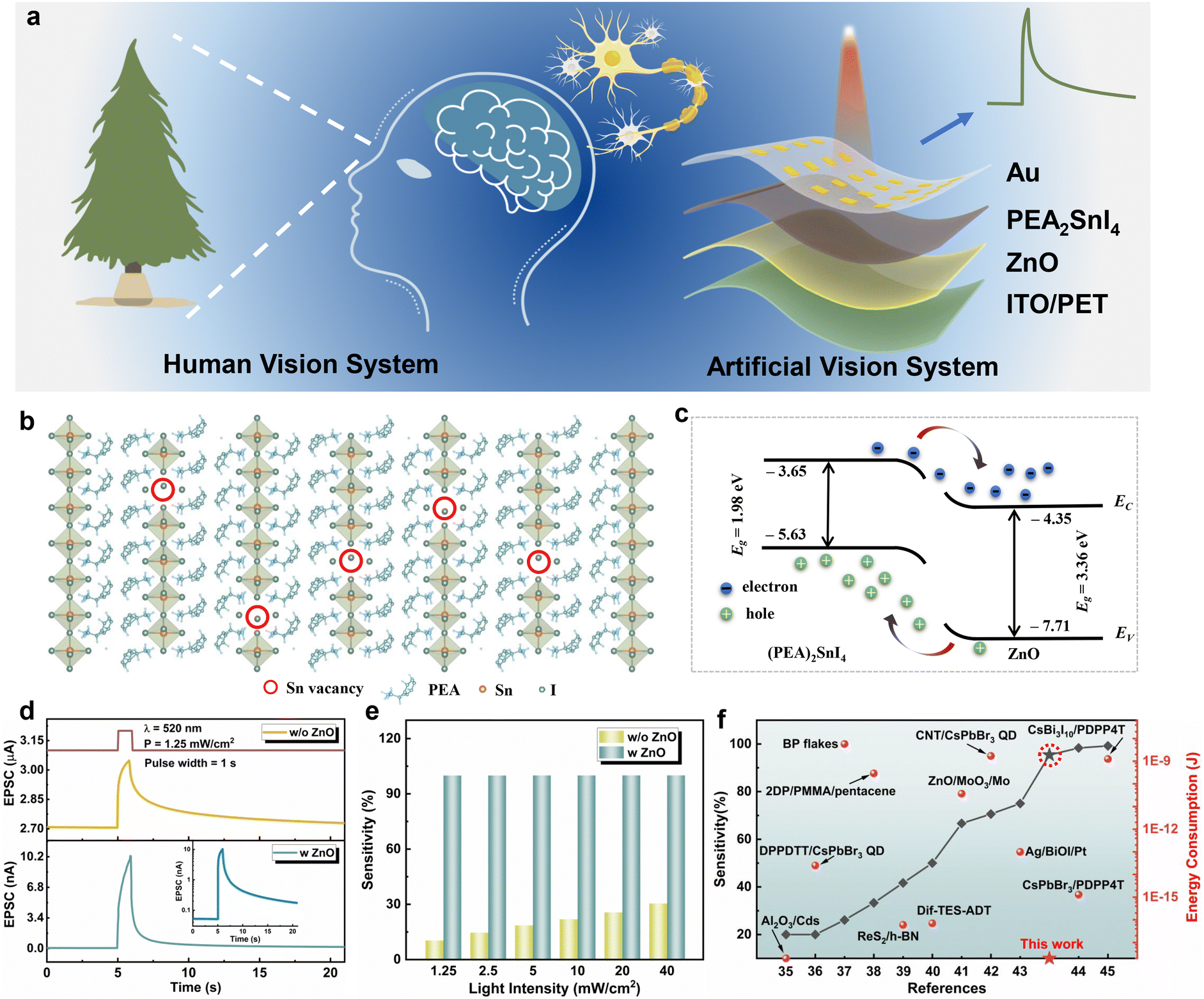 | ||
| Fig. 1 (a) Schematic structure of the bionic human vision system and the proposed optoelectronic synaptic device structure. (b) Schematic illustration of Sn vacancy formation in PEA2SnI4 perovskite. (c) Energy band diagram of the PEA2SnI4/ZnO heterojunction under illumination without power supply. (d) EPSC behavior of the Au/PEA2SnI4/ITO and Au/PEA2SnI4/ZnO/ITO device triggered by a light pulse (inset shows the graph of the corresponding logarithm). (e) S versus light intensity of the two types of devices. (f) Comparison of customized sensitivity and energy consumption from previously reported devices.35–45 | ||
On this basis, to estimate the effect of the device's optoelectronic performance with and without the ETL, EPSC characteristic was studied under the same light condition (520 nm, 1.25 mW cm−2). As shown in Fig. 1(d), the dark current is as high as 2.70 μA in the Au/PEA2SnI4/ITO device, and the current continuously increases to 3.02 μA during the 1 s lighting process. When the ETL is applied, the dark current decreases by 5 orders of magnitude, and the current continuously increases from 15 pA to 10 nA during the 1 s lighting process. This result is consistent with the above discussion. To evaluate the difference more clearly and intuitively, the sensitivity (S) as a function of light intensity is plotted in Fig. 1(e), which can be described as follows:
| S = (Ilight − Idark)/Ilight × 100% | (1) |
| ΔE = V × I × Δt | (2) |
As is well known, the Sn2+ in Sn-based perovskites is readily oxidized to Sn4+ due to its inherently low redox potential,47,48 resulting in poor stability and hindering its development. Here, the 2D PEA2SnI4 perovskite films are synthesized by a simple solution method, and a small amount of SnF2 was used as an additive to create a reducing atmosphere. To verify the film quality, a scanning electron microscope (SEM), X-ray diffraction (XRD), and X-ray photoelectron spectroscopy (XPS) were performed. The SEM images show that the as-prepared films exhibit a complete and uniform coverage morphology (Fig. 2(a)). According to the results of atomic force microscopy (AFM) measurement in Fig. S4 (ESI†), the surface roughness of 15.9 nm was obtained, which indicates the homogeneity of the as-prepared films. Furthermore, the elemental composition and distribution in PEA2SnI4 films were investigated by energy dispersive spectrometer (EDS) measurements (Fig. 2(a)), which shows that the Sn and I elements are uniformly distributed in the films. Furthermore, the elemental atomic ratio is 1![[thin space (1/6-em)]](https://www.rsc.org/images/entities/char_2009.gif) :3.78 (Fig. S5, ESI†), which is close to the stoichiometric ratio in PEA2SnI4, indicating that the perovskite films were successfully prepared. The XRD pattern (Fig. 2(c)) of the films shows obvious diffraction peaks to be located at 5.5°, 10.9°, 16.4°, 21.9°, 27.4°, 33.0°, which are consistent with the (0 0 n) (n = 2, 4, 6, 8, 10, 12) diffraction peaks of 2D perovskites, confirming the phase purity.49,50 To determine the composition of the prepared PEA2SnI4 films, XPS measurements were carried out (Fig. S6, ESI†). The binding energy at 630.2 and 618.8 eV is attributable to I 3d3/2 and I 3d5/2, respectively. Fig. 2(d) shows the high-resolution spectra of the characteristic element Sn 3d. The Sn 3d core level exhibits two peaks at 495.6 and 487.1 eV, corresponding to Sn 3d3/2 and Sn 3d5/2, respectively, suggesting the phase purity of the as-prepared films. Furthermore, to verify the stability of the pure PEA2SnI4 films prepared in this paper, we recorded the optical photographs and performed XRD measurements after placing the films in an ambient environment (20 °C, 35–45% humidity) for 8 h, as shown in Fig. S7 and S8 (ESI†). It can be seen that the prepared PEA2SnI4 film maintains strong luminescence after being placed in the air for 8 h. The XRD pattern reveals that the PEA2SnI4 film has no obvious decomposition. Compared with the reported work,48 the stability of the pure PEA2SnI4 films prepared in this paper was significantly improved. The cross-sectional SEM image of the device is shown in Fig. 2(b), which illustrates the structure of each layer clearly. The ZnO layer grown by the atomic layer deposition (ALD) method is shown in Fig. S9 (ESI†), which has a dense and uniform surface without any holes. The roughness of the film was 0.78 nm. The optical properties of PEA2SnI4, ZnO, and PEA2SnI4/ZnO films were evaluated by UV-Vis absorption spectroscopy (Fig. 2(e)), where PEA2SnI4 displays a clear and well-defined absorption edge at 650 nm. Meanwhile, the absorption edge of ZnO is located at about 380 nm in the UV region, corresponding to a wide band gap of 3.36 eV. The absorption spectra show that the device can effectively detect UV to red light. The photoluminescence (PL) spectra show that the PEA2SnI4 film possesses an emission peak at 623 nm. Here, we discussed the charge-transfer efficiency through the comparison of spectra from steady-state PL and the PL decay transient. As shown in Fig. S10a (ESI†), the hybrid films exhibit a weaker spectrum than the PEA2SnI4 film, and the integral intensity decreased by ≈92.94%. The PL decay transient spectrum under 375-nm optical excitation is shown in Fig. S10b (ESI†). The average lifetimes of the films are extracted using the exponential fitting method and calculated to be 4.08 ns and 3.71 ns without and with the ZnO layer, respectively. The above results indicate that the photogenerated carriers are effectively transferred in the hybrid structure. Therefore, the ZnO layer can be regarded as the ETL, which reduces the possibility of the recombination of holes and electrons.
:3.78 (Fig. S5, ESI†), which is close to the stoichiometric ratio in PEA2SnI4, indicating that the perovskite films were successfully prepared. The XRD pattern (Fig. 2(c)) of the films shows obvious diffraction peaks to be located at 5.5°, 10.9°, 16.4°, 21.9°, 27.4°, 33.0°, which are consistent with the (0 0 n) (n = 2, 4, 6, 8, 10, 12) diffraction peaks of 2D perovskites, confirming the phase purity.49,50 To determine the composition of the prepared PEA2SnI4 films, XPS measurements were carried out (Fig. S6, ESI†). The binding energy at 630.2 and 618.8 eV is attributable to I 3d3/2 and I 3d5/2, respectively. Fig. 2(d) shows the high-resolution spectra of the characteristic element Sn 3d. The Sn 3d core level exhibits two peaks at 495.6 and 487.1 eV, corresponding to Sn 3d3/2 and Sn 3d5/2, respectively, suggesting the phase purity of the as-prepared films. Furthermore, to verify the stability of the pure PEA2SnI4 films prepared in this paper, we recorded the optical photographs and performed XRD measurements after placing the films in an ambient environment (20 °C, 35–45% humidity) for 8 h, as shown in Fig. S7 and S8 (ESI†). It can be seen that the prepared PEA2SnI4 film maintains strong luminescence after being placed in the air for 8 h. The XRD pattern reveals that the PEA2SnI4 film has no obvious decomposition. Compared with the reported work,48 the stability of the pure PEA2SnI4 films prepared in this paper was significantly improved. The cross-sectional SEM image of the device is shown in Fig. 2(b), which illustrates the structure of each layer clearly. The ZnO layer grown by the atomic layer deposition (ALD) method is shown in Fig. S9 (ESI†), which has a dense and uniform surface without any holes. The roughness of the film was 0.78 nm. The optical properties of PEA2SnI4, ZnO, and PEA2SnI4/ZnO films were evaluated by UV-Vis absorption spectroscopy (Fig. 2(e)), where PEA2SnI4 displays a clear and well-defined absorption edge at 650 nm. Meanwhile, the absorption edge of ZnO is located at about 380 nm in the UV region, corresponding to a wide band gap of 3.36 eV. The absorption spectra show that the device can effectively detect UV to red light. The photoluminescence (PL) spectra show that the PEA2SnI4 film possesses an emission peak at 623 nm. Here, we discussed the charge-transfer efficiency through the comparison of spectra from steady-state PL and the PL decay transient. As shown in Fig. S10a (ESI†), the hybrid films exhibit a weaker spectrum than the PEA2SnI4 film, and the integral intensity decreased by ≈92.94%. The PL decay transient spectrum under 375-nm optical excitation is shown in Fig. S10b (ESI†). The average lifetimes of the films are extracted using the exponential fitting method and calculated to be 4.08 ns and 3.71 ns without and with the ZnO layer, respectively. The above results indicate that the photogenerated carriers are effectively transferred in the hybrid structure. Therefore, the ZnO layer can be regarded as the ETL, which reduces the possibility of the recombination of holes and electrons.
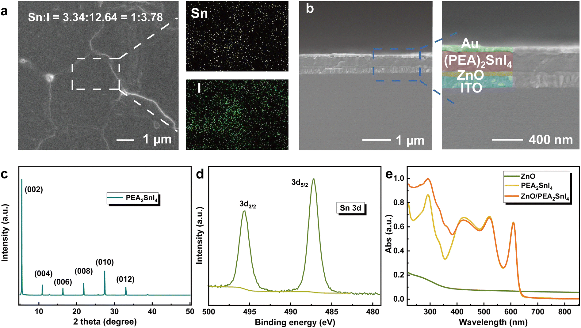 | ||
| Fig. 2 (a) Top-view SEM image of PEA2SnI4 and mapping images for the corresponding elements (Sn and I). (b) Cross-sectional image of the PEA2SnI4/ZnO device. (c) XRD pattern of PEA2SnI4 film. (d) XPS spectra of PEA2SnI4: Sn 3d. (e) Absorption spectrum of ZnO, PEA2SnI4, and the PEA2SnI4/ZnO films. | ||
In the human visual systems, the retina contains three types of photoreceptor cells that can recognize red, green, and blue color signals. When light signals are delivered to the retina, cone and rod cells convert the light signals into electrical signals, which in turn are transmitted to the brain through a network of synapses (Fig. 3(a)).51 As a result, the range of light sensitivity in human eyes is 380–780 nm, which leads to the inability of the human eye to perceive UV light. Here, based on the ability of the device for wide-spectrum light detection (200–650 nm), tetrachromatic vision perception was investigated. As shown in Fig. 3(b), the EPSC curves of the device under 320-nm, 450-nm, 520-nm, and 635-nm illumination (with a calibrated light intensity of 0.4 mW cm−2) are shown, suggesting that the device has the potential to expand the range of applications for human eye recognition. On this basis, the basic synaptic plasticity of Au/PEA2SnI4/ZnO/ITO was investigated. PPF is used to evaluate and reflect the connection strength between presynaptic and postsynaptic membranes and is an important indication of short-term plasticity (STP). As shown in Fig. 3(c), the PPF behavior of the heterojunction device was successfully simulated using two identical successive pulses with an interval time (Δt) of 1 s (520 nm, 1.25 mW cm−2, duration of 1 s). We can observe that the second spike is higher than the first response peak when the second pulse is applied. This is attributed to the trapped electrons generated by the first pulse taking a long time to escape, while the second pulse generates additional photogenerated carriers, resulting in an accumulation of current.52 To further evaluate the PPF properties, the PPF index was introduced, which can be described as PPF = A2/A1 × 100%, where A1 and A2 are the photocurrent values triggered by the first and second light pulse, respectively. As shown in Fig. 3(d), the maximum PPF index is 128% at Δt of 70 ms under 0 V bias. In addition, as Δt increased, the PPF index decayed exponentially.
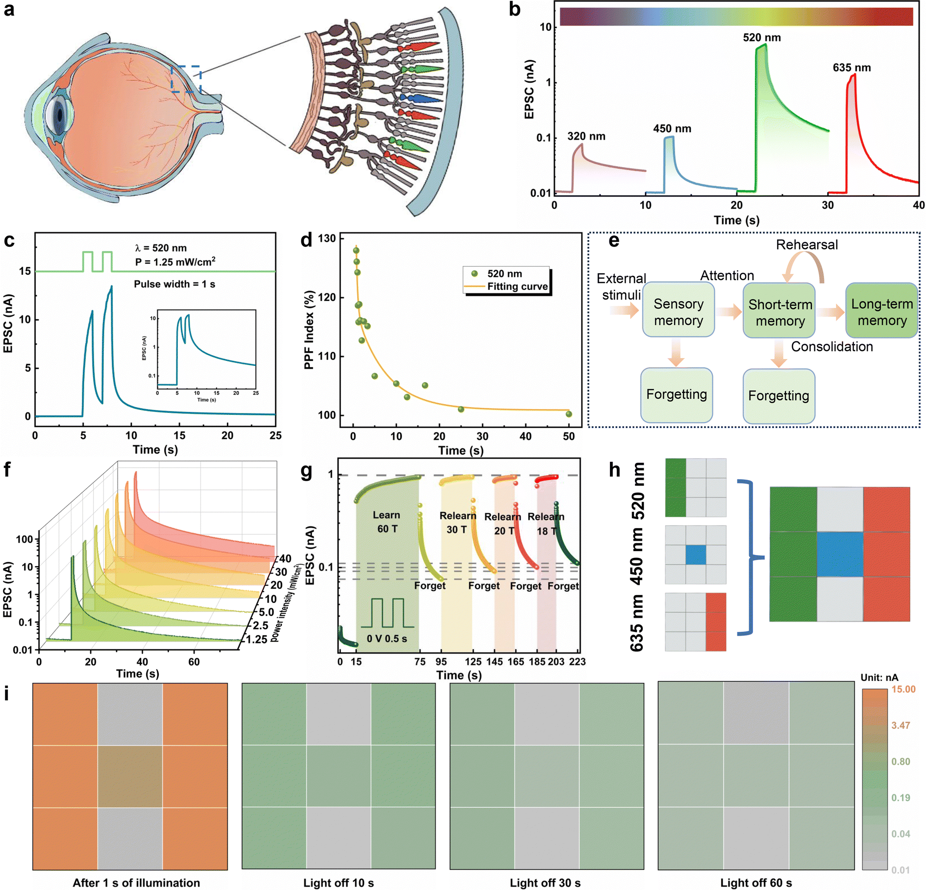 | ||
| Fig. 3 (a) Schematic representation of the human visual system. The EPSC behavior was triggered by (b) 320-nm, 450-nm, 520-nm, and 635-nm illumination (0.4 mW cm−2) and (c) two successive light pulses (520 nm, 1.25 mW cm−2). (d) PPF index expressed as a function of optical pulse widths. (e) Learning and memory processes demonstrate the transition of STM to LTM in human brains. (f) EPSC behavior is triggered by different light power densities (520 nm, pulse width of 1 s). (g) Normalized “learning-forgetting” experience of the device. (h) Schematic diagram of a 3 × 3 synaptic device array (the different colors represent different areas exposed to different light wavelengths). (i) Multicolor recognition and memorization of a 3 × 3 array with the input image of the letter “H”. | ||
In the human brain, memory is strengthened by repeated learning training, which transforms short-term memory (STM) into long-term memory (LTM; Fig. 3(e)). Therefore, we further explored synaptic plasticity by varying the light intensity, light pulse number, and light width. The input light pulse stimulation is regarded as the training process, while the resulting postsynaptic current is defined as the memory level. As shown in Fig. S11 (ESI†) and Fig. 3(f), the EPSC of the device increases significantly as the light intensity increases from 17 μW cm−2 to 40 mW cm−2 at a light pulse width of 1 s. The device can maintain a longer forgetting time after high light-intensity excitation, which is like the memorization process in the human brain. Similarly, the transition from STM to LTM can be achieved by increasing the pulse number and the light duration time as well, as shown in Fig. S12 (ESI†). Furthermore, synaptic plasticity enables the human brain to undergo a “learning-forgetting-relearning” process when acquiring new knowledge. Fig. 3(g) sheds light on the learning experience behavior of the device (520 nm, 1.25 mW cm−2, 1 Hz). The EPSC was significantly increased by the first 60 light pulses and then decayed spontaneously after the light was removed. This process corresponds to the learning-forgetting part. In the relearning process, the EPSC returns to the initial level, only 30 light pulses for the second training process, and 20 light pulses for the third training process were applied. The EPSC maintained a higher value than the previous period after 20 seconds of decay. This phenomenon is like the Ebbinghaus forgetting curve. It takes less time to relearn the amnesic information, but the memory can be strengthened after the relearning process. Then, the visual perception and memory function is emulated by a 3 × 3 array, as shown in Fig. S13a (ESI†). The optical image of the test process is shown in Fig. S13b (ESI†), where a mask plate containing a capital letter “T” was placed between the light source and the device. The postsynaptic currents after 1 s of illumination were collected point by point and are plotted in Fig. S13c (ESI†). After 5 s of forgetting, the EPSC of the area illuminated by light is 20 times that of the dark current, illustrating the great potential of this synaptic array for image storage and learning.
Subsequently, the flexible stability of the array device was conducted under different bending angles. Fig. S14a (ESI†) shows the corresponding optical images, and the inset in the upper right corner presents the top view of the bending process. The EPSC behavior at different bending angles is summarized in Fig. S14b (ESI†). It can be found that the postsynaptic current and the trend of change are almost the same at the bending angle of 0°, 60°, 90°, and 120°. Then, the EPSC behavior after different bending numbers under the bending angle of 90° was tested. Fig. S14c (ESI†) plots the change in EPSC value after 0 and 10 s of no light, with an interval of 10 cycles; the test process is shown in Video S1 (ESI†). No obvious performance degradation is found after 500 bending cycles, which indicates that the flexible device has a wonderful bending endurance.
Finally, based on the ability of wide spectrum light detection (200–650 nm) of the device, the potential of synaptic devices with 3 × 3 arrays for multicolor perception is further studied. Light of 450 nm (B)/520 nm (G)/635 nm (R) was fixed at 1.25 mW cm−2. As shown in Fig. 3(h), different regions are illuminated with different colors, and a capital letter “H” is finally formed. The array devices were first stimulated by a light pulse of 1 s, and the light was then removed to obtain the EPSC at different forgetting times; the results are plotted in Fig. 3(i). The device can clearly distinguish the shape of “H” within the time scale of 60 s, which means that the device can perceive and memorize RGB light pulses, laying the foundation to simulate trichromatic vision. Furthermore, by exploiting the response properties of the devices to wavelength and light intensity, the device is applied to light communication applications. As shown in Fig. S15a (ESI†), the EPSC values after 1 s of light illumination at 450 nm (420 μW cm−2; B), 520 nm (1.25 mW cm−2; G), and 635 nm (420 μW cm−2; R) are 0.1 nA, 10.4 nA, and 1.4 nA, respectively, which are defined as 00/01/10 (according to the American Standard Code for Information Interchange (ASCII) rules). The three light pulses GBBR, GBRG, and GGGB represent 01000010, 01001001, and 01010100, respectively; they can be demodulated into the “BIT” letters and stored in the device (Fig. S15b, ESI†). When the light is removed, the accuracy of the information transfer can still be guaranteed due to the significant difference in the current magnitude. It is worth noting that the device is capable of simple imaging, decoding, and storage of multicolor light signals, which can be used in multifunctional optoelectronic devices.
Due to its high energy and penetrating ability, UV light is prone to cause irreparable damage to the retina of the human eye as well as to the human skin, especially UV-A (320–400 nm), which is only slightly absorbed by the ozone layer and clouds. However, the human eye cannot sense UV light. Therefore, perceiving and recognizing invisible UV light plays a crucial role in exploiting artificial visual perception systems and human life. In this work, the Au/PEA2SnI4/ZnO/ITO device demonstrates remarkable perception and memorization of UV light, and on this basis, a simulation of sunburn on the skin under UV exposure was presented. It is worth noting that this study not only targets sunburn simulation on human skin, but complements the approach to UV prevention as a universal tool. As shown in Fig. 4(a), when human skin tissue is exposed to UV light, the brain cannot send a timely danger signal because the human eye cannot recognize UV light. Only when the skin shows symptoms, such as swelling, sun-spots, or even peeling, the human brain will send feedback to the muscle nerves to take corresponding protective measures, but it is too late. Therefore, we propose a sunburn simulation model based on different EPSCs for different degrees of sunburn. Specifically, the hierarchical simulation of different light intensities (0.43–1.55 mW cm−2), different exposure times (1–20 s), and different intervals (1–15 s) for skin sunburn is explored. As shown in Fig. 4(b), with a fixed light wavelength of 320 nm and an exposure time of 1 s, it can be seen that the EPSC increases dramatically with the increase in light intensity, which corresponds to the simulation of sunburn of human skin at different UV intensities. Here, the postsynaptic current increment (ΔPSC) of 200 pA is defined as the threshold current for skin damage, and ΔPSC/threshold is defined as the pain facilitation parameter. It is obvious that at low UV intensities, the ΔPSC is much smaller than the safe current (Fig. 4(e)), which is supposed to prove the safe state of human skin at weak UV light intensity. The effect of different exposure times on ΔPSC at the same light intensity (1.25 mW cm−2) is shown in Fig. 4(c). At an exposure time of 1 s, the current value is less than the threshold, but when the exposure time increases to 2 s, the PSC immediately exceeds the threshold (Fig. 4(f)). This phenomenon is similarly to that for an increase in skin exposure time to UV further increasing the risk of skin damage. Finally, as shown in Fig. 4(d) and (g), the simulation of two adjacent intervals of time Δt (1–15 s) for skin sunburn is also explored. When the interval is 1 s and 2 s, the ΔPSC is 235 pA and 210 pA, causing skin damage. When the interval time exceeds 2 s, the ΔPSC is lower than the threshold current. The pain facilitation parameter gradually increases with an increase in the UV intensities and the exposure time, and it decreases with increased intervals between two consecutive UV pulses. This is like the skin damage process. The model for simulating human skin sunburn using UV synaptic devices may provide new ideas for future artificial sensory systems.
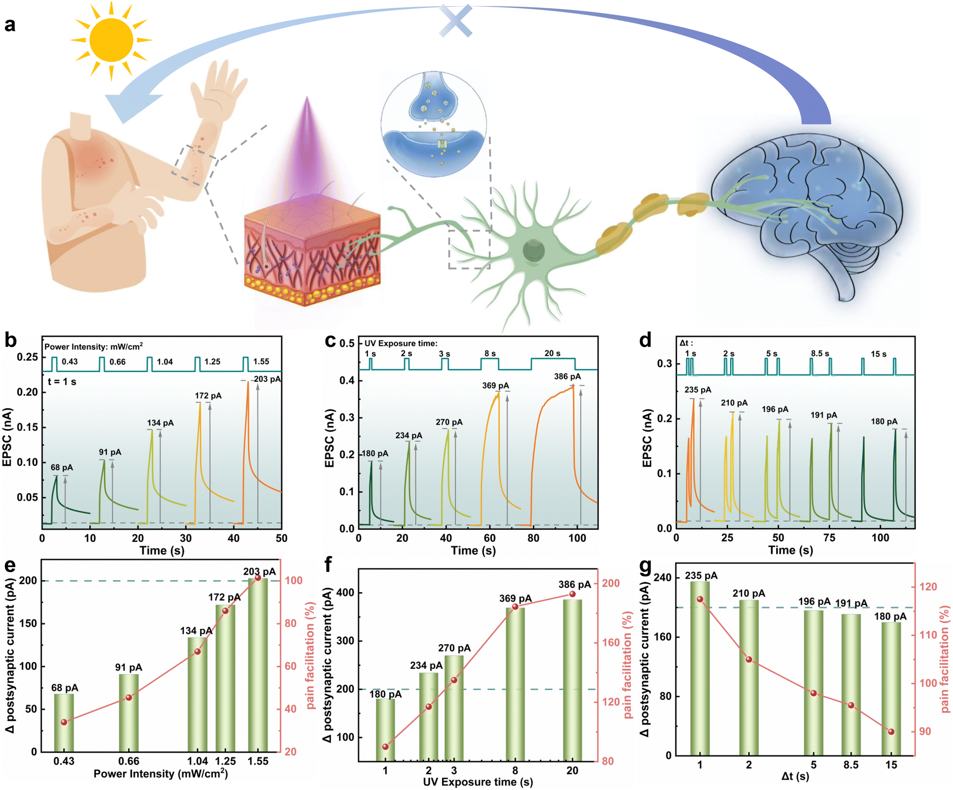 | ||
| Fig. 4 (a) Schematic diagram of the device detecting, recognizing, and self-protecting against UV stimuli. (b) EPSC and (e) ΔPSC and pain facilitation under different UV irradiation intensities (320 nm, pulse width of 1 s). (c) EPSC and (f) ΔPSC and pain facilitation under different UV irradiation times (320 nm, 1.25 mW cm−2). (d) EPSC and (g) ΔPSC and pain facilitation under different UV irradiation intervals (320 nm, 1.25 mW cm−2). | ||
To further validate the proposed concept and the reliability of the device, we prepared a wearable UV monitor by integrating the device into the integrated circuit and recorded the ΔPSC under different UV exposure conditions in real-time. The visualized data is presented on a smartphone via wireless communication. The schematic diagram of UV monitoring is shown in Fig. 5(a), including sensing, controlling, displaying, and battery modules. In detail, the sensing module of the Au/PEA2SnI4/ZnO/ITO device converts light signals into current signals, which are processed by an inverter, amplifier, and low-pass filter, before being converted by a microcontroller unit (MCU). They are finally transmitted to the mobile phone via a Bluetooth terminal. A lithium battery is used for power supply (Fig. 5(c)). Eventually, the visualized data will be presented on the user's interface, displaying the ΔPSC in different outdoor environments in real-time as well as the corresponding UV indexes, thus enabling precise prevention and reducing the risk of skin sunburn. Specific experimental operations are presented in Video S2 (ESI†), where a sunlight simulator was used to simulate the outdoor sunlight, and a UV filter was used to exclude the interference from other colors of light. According to Video S2 (ESI†), it can be seen that after the same exposure time, the skin will become “Hurt” after strong UV light exposure (>1 sun condition with a 365-nm narrow band filter). Even after self-healing for 40 s, it still cannot be recovered, which means that the skin has already been irreversibly damaged. During moderate light exposure (0.5–1 sun condition), the EPSC rises to the skin damage threshold, and the “Exposure safety” returns from the “Hurt” state to the “Heal” state after withdrawing from light for 40 s, corresponding to the skin's self-repair process. Finally, when exposed to weak light, the skin will not be harmed at all, indicating that humans could spend a long time outdoors at this time. The measurements can be used to confirm the potential application of utilizing UV synapses in the prevention of various skin diseases caused by excessive UV exposure. Finally, the designed wearable UV monitoring was successfully used in an outdoor environment as shown in Video S3 (ESI†) (three times, i.e., the times 14:00, 15:30, and 16:30 were chosen for testing, respectively). In addition, the flexible UV monitoring device can easily be attached to the skin, canvas bags, and sun hats, as shown in Fig. 5(b) and Fig. S16 (ESI†), so that the risk of direct exposure to the outdoor environment during any moment of the day can be obtained through the proposed UV monitoring system.
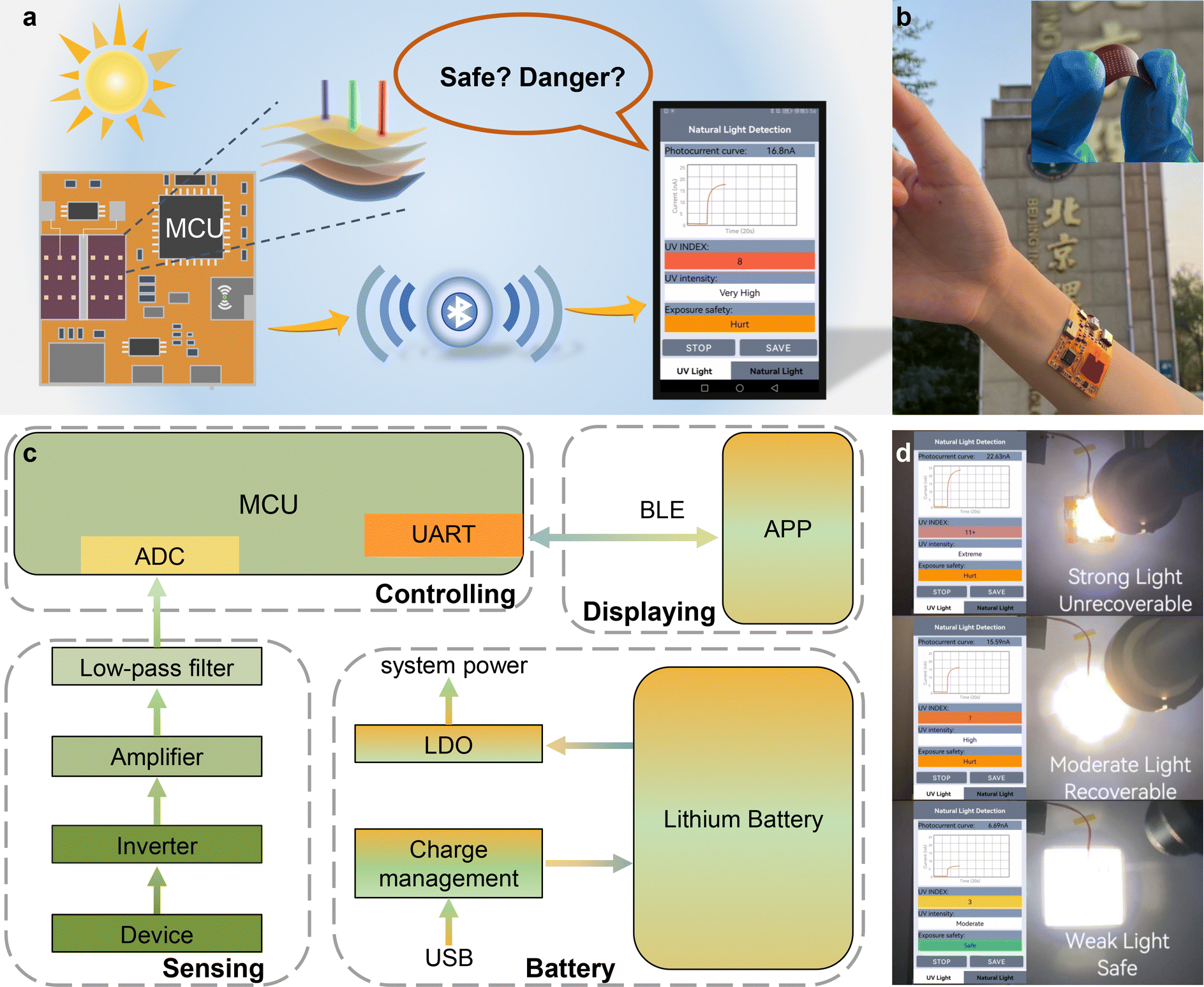 | ||
| Fig. 5 (a) Diagram of the brief working principle of UV monitoring. The data can be transmitted to the user’s mobile phone via Bluetooth terminal for real-time display. (b) Photograph of the designed flexible circuit board on arm (the inset shows the flexible device). (c) System-level block diagram of the flexible UV monitor. (d) Real-time display of skin exposure status under different standards of solar illumination. | ||
Conclusions
In summary, a flexible optoelectronic synapse with the structure of Au/PEA2SnI4/ZnO/ITO was successfully constructed. By introducing the ETL of ZnO, the dark current of the device is decreased by 5 orders of magnitude compared to the Au/PEA2SnI4/ITO device, and the sensitivity is increased from 10.3 to 99.2% at 1.25 mW cm−2 light illumination (520 nm), indicating the important role of the introduced ETL in promoting the separation of excitons at the interface and inhibiting the free carrier transfer. Moreover, the vertical synaptic device can operate without an external power supply, and the energy consumption is quite advantageous compared with other synaptic devices. The optoelectronic synaptic functions with integrated sensing, recognition, and memory features were successfully realized in the synaptic device. The UV-Vis sensitive and tunable synaptic plasticity of the array device enables multicolor recognition and skin sunburn simulation. Finally, a wearable UV monitor was fabricated by integrating the flexible device in the integrated circuit and used for skin sunburn warning, which enables real-time monitoring of UV light and real-time presence on users’ interfaces, reducing skin cancer caused by prolonged exposure to UV light. These results may provide a novel strategy to facilitate multicolor vision sensors and create the possibility of integrated sensing-memory processing for the fabrication of artificial vision systems in the future.Experimental section
Synthesis of PEA2SnI4 films
PEAI (C6H5C2H4NH3I, 99.5%) was purchased from Xi’an Yuri Solar Co., Ltd. Tin(II) iodide powder (SnI2, 99.999%) was purchased from Alfa Aesar. The solvents dimethylformamide (DMF, ≥99.5%) and dimethyl sulfoxide (DMSO, ≥99.5%) were purchased from Aladdin. Chlorobenzene (99.8%) and tin(II) fluoride (98%) were purchased from Innochem. A mixture of 0.6 M of PEAI powder, 0.3 M of SnI2 powder, and a small amount of SnF2 powder was dissolved in a mixture of DMSO and DMF (volume 1:4, respectively). The mixed solution was stirred at 80 °C for 5 h, and the precursor was filtered through a 0.22-μm polyvinylidene fluoride (PVDF) filter.
Preparation of multiarray PEA2SnI4/ZnO devices
In this work, commercially available PET/ITO was used as the substrates, which were ultrasonically cleaned for 15 min with acetone, ethanol, and deionized water, respectively. Subsequently, ETL ZnO was prepared by ALD. The deposition temperature was set to 60 °C. The substrates were then treated with oxygen plasma for 10 min and immediately placed in a glove box to spin-coat the PEA2SnI4 perovskite films. Spin-coating was performed at a low speed of 500 rpm/10 s followed by a high speed of 3000 rpm/60 s. Then, 20 μL of chlorobenzene was added quickly at the end of the spin-coating countdown of 10 s. The films were then annealed for 15 min at 80 °C to evaporate the solvents and to promote crystallization. After the above films were prepared, Cr/Au electrodes (10/50 nm) were deposited on PEA2SnI4 films by thermal evaporation using a shadow mask.Characterization of materials and devices
Field emission scanning electron microscopy (FESEM, Zeiss SUPRA 55, 5 keV) was used to capture the surface morphology of the prepared PEA2SnI4 films. Besides, elemental mapping images of Sn and I were obtained using EDS. The crystallinity of the films was examined using Cu Kα radiation with XRD (DMAX-RB). Both UPS and XPS data were measured by AXIS SUPRA. The absorption spectra were measured using a Shimadzu UV-3150 spectrophotometer. The PL and TRPL spectra were obtained by photoluminescence spectrometer (FLS1000). The photoresponse behaviors of the constructed artificial synapses were obtained by probe stage and semiconductor characterization system (B1500, Keysight).Conflicts of interest
There are no conflicts to declare.Acknowledgements
This work was supported by the National Natural Science Foundation of China (no. 61888102, 61625404, and 62304021). No formal approval for the experiments related to wearable skin technologies involving human volunteers was required by the authors’ institute. Volunteers took part following informed consent.Notes and references
- I. Boybat, M. Le Gallo, S. R. Nandakumar, T. Moraitis, T. Parnell, T. Tuma, B. Rajendran, Y. Leblebici, A. Sebastian and E. Eleftheriou, Nat. Commun., 2018, 9, 2514 CrossRef PubMed.
- C. Zhu, H. Liu, W. Wang, L. Xiang, J. Jiang, Q. Shuai, X. Yang, T. Zhang, B. Zheng, H. Wang, D. Li and A. Pan, Light: Sci. Appl., 2022, 11, 337 CrossRef CAS PubMed.
- Z. Yu, A. M. Abdulghani, A. Zahid, H. Heidari, M. A. Imran and Q. H. Abbasi, IEEE Access, 2020, 8, 67085 Search PubMed.
- S. Subbulakshmi Radhakrishnan, A. Sebastian, A. Oberoi, S. Das and S. Das, Nat. Commun., 2021, 12, 2143 CrossRef CAS PubMed.
- D. Marković, A. Mizrahi, D. Querlioz and J. Grollier, Nat. Rev. Phys., 2020, 2, 499 CrossRef.
- S. Fan, E. Wu, M. Cao, T. Xu, T. Liu, L. Yang, J. Su and J. Liu, Mater. Horiz., 2023, 10, 4317 RSC.
- J. Du, D. Xie, Q. Zhang, H. Zhong, F. Meng, X. Fu, Q. Sun, H. Ni, T. Li, E.-J. Guo, H. Guo, M. He, C. Wang, L. Gu, X. Xu, G. Zhang, G. Yang, K. Jin and C. Ge, Nano Energy, 2021, 89, 106439 CrossRef CAS.
- T. Xie, Q. Wang, M. Li, Y. Fang, G. Li, S. Shao, W. Yu, S. Wang, W. Gu, C. Zhao, M. Tang and J. Zhao, Adv. Funct. Mater., 2023, 33, 2303970 CrossRef CAS.
- K. Dong, H. Zhou, Z. Gao, M. Xu, L. Zhang, S. Zhou, H. Cui, S. Wang, C. Tao, W. Ke, F. Yao and G. Fang, Adv. Funct. Mater., 2023, 34, 2306941, DOI:10.1002/adfm.202306941.
- T. Jiang, Y. Wang, Y. Zheng, L. Wang, X. He, L. Li, Y. Deng, H. Dong, H. Tian, Y. Geng, L. Xie, Y. Lei, H. Ling, D. Ji and W. Hu, Nat. Commun., 2023, 14, 2281 CrossRef CAS PubMed.
- N. Hu, D. Gao, X. Cai, L. Lei, W. Wang, H. Fan, P. Müller-Buschbaum and Q. Zhong, Adv. Opt. Mater., 2022, 11, 2202248 CrossRef.
- W. Kurz, A. K. Yetisen, M. V. Kaito, M. J. Fuchter, M. Jakobi, M. Elsner and A. W. Koch, Adv. Opt. Mater., 2020, 8, 1901969 CrossRef CAS.
- Z. Zhang, X. Gao, Y. Zhong, J. Liu, L. Zhang, S. Wang, J. Xu and S. Wang, Adv. Electron. Mater., 2017, 3, 1700052 CrossRef.
- Y. Yoon, Y. Kim, W. S. Hwang and M. Shin, Adv. Electron. Mater., 2023, 9, 2300098 CrossRef CAS.
- S. Cai, C. Zuo, J. Zhang, H. Liu and X. Fang, Adv. Funct. Mater., 2021, 31, 2100026 CrossRef CAS.
- Y. Zheng, Y. Wang, Z. Li, Z. Yuan, S. Guo, Z. Lou, W. Han, G. Shen and L. Wang, Matter, 2023, 6, 506 CrossRef CAS.
- C. Zuo, L. Zhang, X. Pan, H. Tian, K. Yan, Y. Cheng, Z. Jin, C. Yi, X. Zhang, W.-Q. Wu, Q. Bao, L. Han and L. Ding, Nano Res., 2023, 16, 10256 CrossRef CAS.
- S. Jiang, R. Huang, W. Li, X. Huang, H. Sheng, F. Wu, Y. Lv, Y. Fu, C. Zhao and W. Mai, ACS Appl. Mater. Interfaces, 2022, 14, 26279 CrossRef CAS PubMed.
- Z. Liu, Z. Zhang, X. Zhang, X. Li, Z. Liu, G. Liao, Y. Shen and M. Wang, Nano Lett., 2023, 23, 1181 CrossRef CAS PubMed.
- W. Kong, C. Zhao, T. Huang, X. Li, J. Xing, Z. Yu, P. Yang, W. Li and W. Yu, ACS Appl. Mater. Interfaces, 2022, 14, 28154 CrossRef CAS PubMed.
- X. Huang, Q. Li, W. Shi, K. Liu, Y. Zhang, Y. Liu, X. Wei, Z. Zhao, Y. Guo and Y. Liu, Small, 2021, 17, e2102820 CrossRef PubMed.
- Y. Sun, L. Qian, D. Xie, Y. Lin, M. Sun, W. Li, L. Ding, T. Ren and T. Palacios, Adv. Funct. Mater., 2019, 29, 1902538 CrossRef.
- H. Dong, C. Ran, W. Gao, N. Sun, X. Liu, Y. Xia, Y. Chen and W. Huang, Adv. Energy Mater., 2022, 12, 2102213 CrossRef CAS.
- S. Shao, J. Liu, G. Portale, H. H. Fang, G. R. Blake, G. H. ten Brink, L. J. A. Koster and M. A. Loi, Adv. Energy Mater., 2017, 8, 1702019 CrossRef.
- J. Qiu, Y. Xia, Y. Zheng, W. Hui, H. Gu, W. Yuan, H. Yu, L. Chao, T. Niu, Y. Yang, X. Gao, Y. Chen and W. Huang, ACS Energy Lett., 2019, 4, 1513 CrossRef CAS.
- C. K. Liu, Q. Tai, N. Wang, G. Tang, H. L. Loi and F. Yan, Adv. Sci., 2019, 6, 1900751 CrossRef PubMed.
- L. Xu, X. Feng, W. Jia, W. Lv, A. Mei, Y. Zhou, Q. Zhang, R. Chen and W. Huang, Energy Environ. Sci., 2021, 14, 4292 RSC.
- L. Qian, Y. Sun, M. Wu, C. Li, D. Xie, L. Ding and G. Shi, Nanoscale, 2018, 10, 6837 RSC.
- C. Chen, X. Zhang, G. Wu, H. Li and H. Chen, Adv. Opt. Mater., 2017, 5, 1600539 CrossRef.
- S. Wang, K. Bidinakis, C. Haese, F. H. Hasenburg, O. Yildiz, Z. Ling, S. Frisch, M. Kivala, R. Graf, P. W. M. Blom, S. A. L. Weber, W. Pisula and T. Marszalek, Small, 2023, 19, 2207426 CrossRef CAS PubMed.
- M. U. K. Sadaf, N. U. Sakib, A. Pannone, H. Ravichandran and S. Das, Nat. Commun., 2023, 14, 5729 CrossRef CAS PubMed.
- S. Wei, Y. Yang, X. Kang, L. Wang, L. Huang and D. Pan, Chem. Commun., 2016, 52, 7265 RSC.
- D. B. M. C. R. Kagan and C. D. Dimitrakopoulos, Science, 1999, 286, 29 CrossRef.
- Y. Li, J. Zhou, Y. Tian, Z. Wei and G. Shen, Small Methods, 2023 DOI:10.1002/smtd.202300026.
- X. Han, Y. Zhang, Z. Huo, X. Wang, G. Hu, Z. Xu, H. Lu, Q. Lu, X. Sun, L. Qiu, P. Yan and C. Pan, Adv. Electron. Mater., 2023, 9, 2201068 CrossRef CAS.
- D. Hao, J. Zhang, S. Dai, J. Zhang and J. Huang, ACS Appl. Mater. Interfaces, 2020, 12, 39487 CrossRef CAS PubMed.
- T. Ahmed, M. Tahir, M. X. Low, Y. Ren, S. A. Tawfik, E. L. H. Mayes, S. Kuriakose, S. Nawaz, M. J. S. Spencer, H. Chen, M. Bhaskaran, S. Sriram and S. Walia, Adv. Mater., 2021, 33, e2004207 CrossRef PubMed.
- J. Zhang, Q. Shi, R. Wang, X. Zhang, L. Li, J. Zhang, L. Tian, L. Xiong and J. Huang, InfoMat, 2021, 3, 904 CrossRef CAS.
- Y. Chen, Y. Kang, H. Hao, X. Xie, J. Zeng, T. Xu, C. Li, Y. Tan and L. Fang, Adv. Funct. Mater., 2022, 33, 2209781 CrossRef.
- J. Shi, J. Jie, W. Deng, G. Luo, X. Fang, Y. Xiao, Y. Zhang, X. Zhang and X. Zhang, Adv. Mater., 2022, 34, e2200380 CrossRef PubMed.
- T. Guo, B. Zhang, X. Wang, Y. Xiao, B. Sun, Y. N. Zhou and Y. A. Wu, Adv. Funct. Mater., 2023, 33, 2303879 CrossRef CAS.
- Q. B. Zhu, B. Li, D. D. Yang, C. Liu, S. Feng, M. L. Chen, Y. Sun, Y. N. Tian, X. Su, X. M. Wang, S. Qiu, Q. W. Li, X. M. Li, H. B. Zeng, H. M. Cheng and D. M. Sun, Nat. Commun., 2021, 12, 1798 CrossRef CAS PubMed.
- P. Lei, H. Duan, L. Qin, X. Wei, R. Tao, Z. Wang, F. Guo, M. Song, W. Jie and J. Hao, Adv. Funct. Mater., 2022, 32, 2201276 CrossRef CAS.
- T. Chen, X. Wang, D. Hao, S. Dai, Q. Ou, J. Zhang and J. Huang, Adv. Opt. Mater., 2021, 9, 2002030 CrossRef CAS.
- R. Wang, P. Chen, D. Hao, J. Zhang, Q. Shi, D. Liu, L. Li, L. Xiong, J. Zhou and J. Huang, ACS Appl. Mater. Interfaces, 2021, 13, 43144 CrossRef CAS PubMed.
- Y. Ran, W. Lu, X. Wang, Z. Qin, X. Qin, G. Lu, Z. Hu, Y. Zhu, L. Bu and G. Lu, Mater. Horiz., 2023, 10, 4438 RSC.
- C. Wang, S. Cui, Y. Ju, Y. Chen, S. Chang and H. Zhong, Adv. Funct. Mater., 2023, 33, 2301304 CrossRef CAS.
- X. Qiu, J. Xia, Y. Liu, P. A. Chen, L. Huang, H. Wei, J. Ding, Z. Gong, X. Zeng, C. Peng, C. Chen, X. Wang, L. Jiang, L. Liao and Y. Hu, Adv. Mater., 2023, 35, 2305648 CrossRef CAS PubMed.
- Y. Ju, X. g Wu, S. Huang, G. Dai, T. Song and H. Zhong, Adv. Funct. Mater., 2021, 32, 2108296 CrossRef.
- G. Vescio, J. Sanchez-Diaz, J. L. Frieiro, R. S. Sanchez, S. Hernandez, A. Cirera, I. Mora-Sero and B. Garrido, ACS Energy Lett., 2022, 7, 3653 CrossRef CAS PubMed.
- M. Huang, W. Ali, L. Yang, J. Huang, C. Yao, Y. Xie, R. Sun, C. Zhu, Y. Tan, X. Liu, S. Li, Z. Li and A. Pan, Adv. Sci., 2023, 10, e2300120 CrossRef PubMed.
- D. Hao, D. Liu, J. Zhang, Y. Wang and J. Huang, Adv. Mater. Technol., 2021, 6, 2100678 CrossRef CAS.
Footnote |
| † Electronic supplementary information (ESI) available. See DOI: https://doi.org/10.1039/d3mh02154h |
| This journal is © The Royal Society of Chemistry 2024 |