
 Open Access Article
 This Open Access Article is licensed under a Creative Commons Attribution-Non Commercial 3.0 Unported Licence
Oxygen tracer diffusion in amorphous hafnia films for resistive memory†
Dongjae
Shin
 a,
Anton V.
Ievlev
b,
Karsten
Beckmann
cd,
Jingxian
Li
a,
Pengyu
Ren
a,
Nathaniel
Cady
c and
Yiyang
Li
*a
a,
Anton V.
Ievlev
b,
Karsten
Beckmann
cd,
Jingxian
Li
a,
Pengyu
Ren
a,
Nathaniel
Cady
c and
Yiyang
Li
*a
aMaterials Science and Engineering, University of Michigan, Ann Arbor, MI, USA. E-mail: yiyangli@umich.edu
bCenter for Nanophase Materials Science, Oak Ridge National Laboratory, Oak Ridge, TN, USA
cCollege of Nanotechnology, Science and Engineering, University at Albany, Albany, NY, USA
dNY CREATES, Albany, NY, USA
First published on 20th March 2024
Abstract
The oxygen diffusion rate in hafnia (HfO2)-based resistive memory plays a pivotal role in enabling nonvolatile data retention. However, the information retention times obtained in HfO2 resistive memory devices are many times higher than the expected values obtained from oxygen diffusion measurements in HfO2 materials. In this study, we resolve this discrepancy by conducting oxygen isotope tracer diffusion measurements in amorphous hafnia (a-HfO2) thin films. Our results show that the oxygen tracer diffusion in amorphous HfO2 films is orders of magnitude lower than that of previous measurements on monoclinic hafnia (m-HfO2) pellets. Moreover, oxygen tracer diffusion is much lower in denser a-HfO2 films deposited by atomic layer deposition (ALD) than in less dense a-HfO2 films deposited by sputtering. The ALD films yield similar oxygen diffusion times as experimentally measured device retention times, reconciling this discrepancy between oxygen diffusion and retention time measurements. More broadly, our work shows how processing conditions can be used to control oxygen transport characteristics in amorphous materials without long-range crystal order.
New conceptsAmorphous hafnium oxide is one of the most important materials for microelectronics, with applications in high-k gate dielectrics, resistive memory, and beyond. In this work, we experimentally measured oxygen tracer diffusion on amorphous HfO2 thin films for the first time using isotope tracking. This differs from previous attempts to measure oxygen transport in amorphous HfO2 that rely on computational simulations and indirect transient current analysis. Using this direct analysis, we show that the oxygen tracer diffusivity in amorphous HfO2 shows a diffusion activation energy of ∼1.5 eV, which is much higher than those previously measured. This higher activation energy reconciles previous discrepancies in the predicted and experimentally measured retention time of resistive memory devices. It furthermore shows that the oxygen diffusion in amorphous HfO2 can be tuned using the processing conditions. |
Introduction
Resistive memories, or memristors, are electronic devices that switch their resistance states using applied currents and voltages. Such devices are highly promising for embedded memory, in-memory computing, and neuromorphic computing.1–4 Most resistive memories are composed of two-terminal structures with metal–insulator–metal structures.5,6 The insulators, often oxides, are critical in determining the properties of resistive memory devices.5Valence-change memory using metal oxides like Ta2O5 or HfO2 is the most promising type of resistive memory due to CMOS process compatibility, fast switching, and long retention, which exceeds 10 years at 85 °C.5,6 Filament-based valence-change memory switches their resistance state through the electrochemical growth or dissolution of oxygen-deficient conducting filaments.7–12 The information retention time depends on the stability of these oxygen-deficient filaments. Over time, the filaments can dissolve due to the diffusion of oxygen ions into the conducting filaments, ultimately resulting in a loss of information, or retention failure.13–15 It is believed that the retention time is related to the characteristic oxygen diffusion time into the nanosized filament within the metal oxides.13–15 This is supported by large numbers of experimental measurements which show an Arrhenius dependence between the temperature and retention time.16–22
Amorphous hafnia (a-HfO2) is one of the most attractive candidates for resistive memory. Despite extensive research, there exists a vast discrepancy between the experimentally measured device retention time and the characteristic oxygen diffusion time inferred from materials characterization measurements. On the one hand, temperature-dependent device retention measurement suggests an oxygen activation energy between 1.2–1.6 eV.16–21 On the other hand, experimental measurements based on transient current analysis23 and oxygen isotope tracer diffusion24 suggest that the activation energy is only ∼0.5 eV. As a result, whereas experiments have shown >10 years of retention at 85 °C,16–21 the expected characteristic diffusion time based on previous oxygen diffusion measurements23,24 for a 10-nm filament is <10 seconds at the same temperature.
In this study, we reconcile this discrepancy by measuring the oxygen tracer diffusion of a-HfO2 films, and compare them with the retention time of HfO2 resistive memory devices fabricated using a 65-nm process on a 300-mm wafer. We reconcile the previous discrepancy by showing that the oxygen tracer diffusion of a-HfO2 has a very similar Arrhenius activation energy (∼1.5 eV) as the device retention time (∼1.4 eV). We further show that atomic layer deposited (ALD) films have about two orders of magnitude lower oxygen diffusivity than sputtered films, despite nominally identical compositions and lack of long-range crystal order. We propose this difference to be a result of the higher density of ALD films. These results provide precise information on the oxygen diffusivities of a-HfO2 thin films and reconciles previous discrepancies between device and materials characterization results.
Results
Retention time for in-line HfO2 resistive memory devices
Embedded HfO2 resistive memory cells were fabricated on a 65-nm process on a 300 mm wafer at the Albany Nanotech Complex, Albany, NY (Fig. 1a and b). The resistive memory cells are built in the W-M1/Cu-M2 line and consists of a 30 nm TiN bottom electrode deposited by sputtering, a ∼5.8 nm a-HfO2 switching layer deposited by atomic layer deposition (ALD), and 6 nm Ti and 40 nm TiN top electrode deposited by sputtering. More details are given in the Experimental methods. In addition, a 10 kΩ tungsten series resistor is patterned on the chip to limit the total current, thereby creating 1R1R structures (Fig. 1a).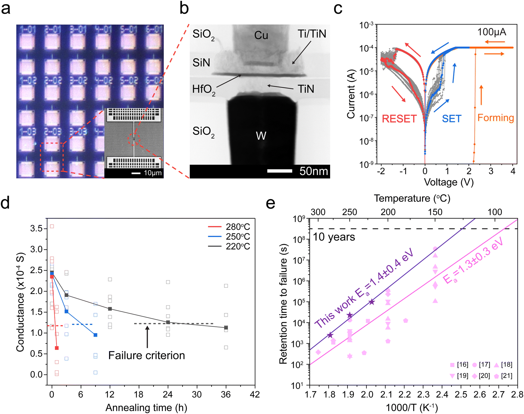 | ||
| Fig. 1 Structure of the HfO2 resistive memory and its performance. (a) Optical image of the array of prepared HfO2 resistive memories. The inset shows an SEM image of a HfO2 resistive memory device. (b) Cross-section TEM image of a typical device. (c) Typical current–voltage (I–V) curves of the HfO2 resistive memory. (d) Evolution of the device conductance upon annealing at different temperatures. The empty squares are conductance values from the 6 devices at each annealing time and temperature (280 °C red, 250 °C blue, and 220 °C black), while the solid squares represent medians calculated from the six conductance values at each annealing time and temperature. The dashed line indicates failure criteria defined as half the conductance value of the initial median. (e) Arrhenius plots of retention times to failure at different temperatures in this work (purple stars) and from previous research (pink symbols). The activation energy of the retention times in this work is 1.4 ± 0.4 eV, while that from the literature is 1.3 ± 0.3 eV.16–21 The errors indicate 2 standard errors in the Arrhenius equation fit. | ||
Fig. 1c shows typical forming, SET, and RESET current–voltage profiles using direct current (DC) voltage sweeps with a 100 μA current compliance (CC). The average HRS resistance is 351![[thin space (1/6-em)]](https://www.rsc.org/images/entities/char_2009.gif) 000 Ω with a range of (98000 ∼ 1200000 Ω), and the average LRS resistance is 4800 Ω with a range of (2800–9000 Ω). This resistance change is believed to result from the formation and dissolution of a conductive filament.
000 Ω with a range of (98000 ∼ 1200000 Ω), and the average LRS resistance is 4800 Ω with a range of (2800–9000 Ω). This resistance change is believed to result from the formation and dissolution of a conductive filament.
After switching, we measure the conductance after annealing a die with many devices at a given temperature. Fig. S1 (ESI†) shows that the resistance increases over time, consistent with the dissolution of the conductive filament. Fig. 1d shows the retention time to failure of the low-resistance state at different temperatures; each temperature experiment contains six devices. Our results show that higher temperatures lead to a faster decrease in conductance, yielding retention failure.
In Fig. 1e, we plot the median retention time for our devices with purple stars. Our results suggest that the retention time t appear to follow the Arrhenius equation, 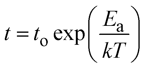 , where the activation energy Ea result from the migration enthalpy of oxygen (vacancy) defects. Based on our results, the activation energy equals 1.4 ± 0.4 eV (two standard errors).
We compare our results to that of previous work16–21 (Fig. 1e). There exists substantial variation in previous reports due to the use of different metallic electrodes, device geometries, and switching conditions (Tables S1 and S2, ESI†). By combining all previous data, we compute their activation energy to be 1.3 ± 0.3 eV, which is very similar to our 1.4 ± 0.4 eV. Consistent with previous reports, the extrapolated retention time exceeds 10 years at 85 °C, satisfying the retention time requirement for nonvolatile memory applications.6,7
We also conducted retention time measurements under different switching conditions. In Fig. S2 (ESI†), we changed the current compliance to 50, 100, and 200 μA. In Fig. S3 (ESI†), we show the retention time after 1000 pulsed switching cycles.25 In Fig. S4 (ESI†), we track the evolution of the HRS conductance. Finally, we conduct retention test at room temperature in Fig. S5 (ESI†). Except for the retention test at room temperature, all other devices showed LRS retention failure and produced slightly different activation energies between 1.2 and 1.5 eV, all within the uncertainty range. In Fig. S6 (ESI†), we combined all retention times, obtained under different switching conditions, and refitted them with the Arrhenius equation. This resulted in the same value of activation energy, 1.4 ± 0.4 eV, as shown in Fig. 1e.
Oxygen tracer diffusion in amorphous HfO2
Next, we investigate oxygen tracer diffusion in amorphous HfO2 thin films deposited by sputtering and by atomic layer deposition. To study oxygen tracer diffusion in sputtered HfO2, we deposited tri-layer samples26 comprised of an 18O-enriched HfO2 layer sandwiched between natural-abundance oxygen HfO2 oxide layers as shown in Fig. 2a; all three layers are nominally identical chemically (HfO2). More details are given in Experimental methods. Afterward, the tri-layer samples are annealed at different temperatures and times to facilitate oxygen tracer diffusion (Fig. 2a). Time of flight secondary ion mass spectrometry (ToF-SIMS) was used to depth-profile the oxygen isotope fraction for both unannealed “pristine” samples and annealed samples (Fig. 2b–e).27 The annealed samples show broadened 18O profiles, signifying oxygen tracer diffusion. These diffusion profiles were fitted (blue line) to Crank's solution, which is an analytical solution to Fick's laws of diffusion.28 Further details are described in Experimental methods. X-ray diffraction (XRD) confirms that such samples are amorphous after these annealing conditions (Fig. S7, ESI†).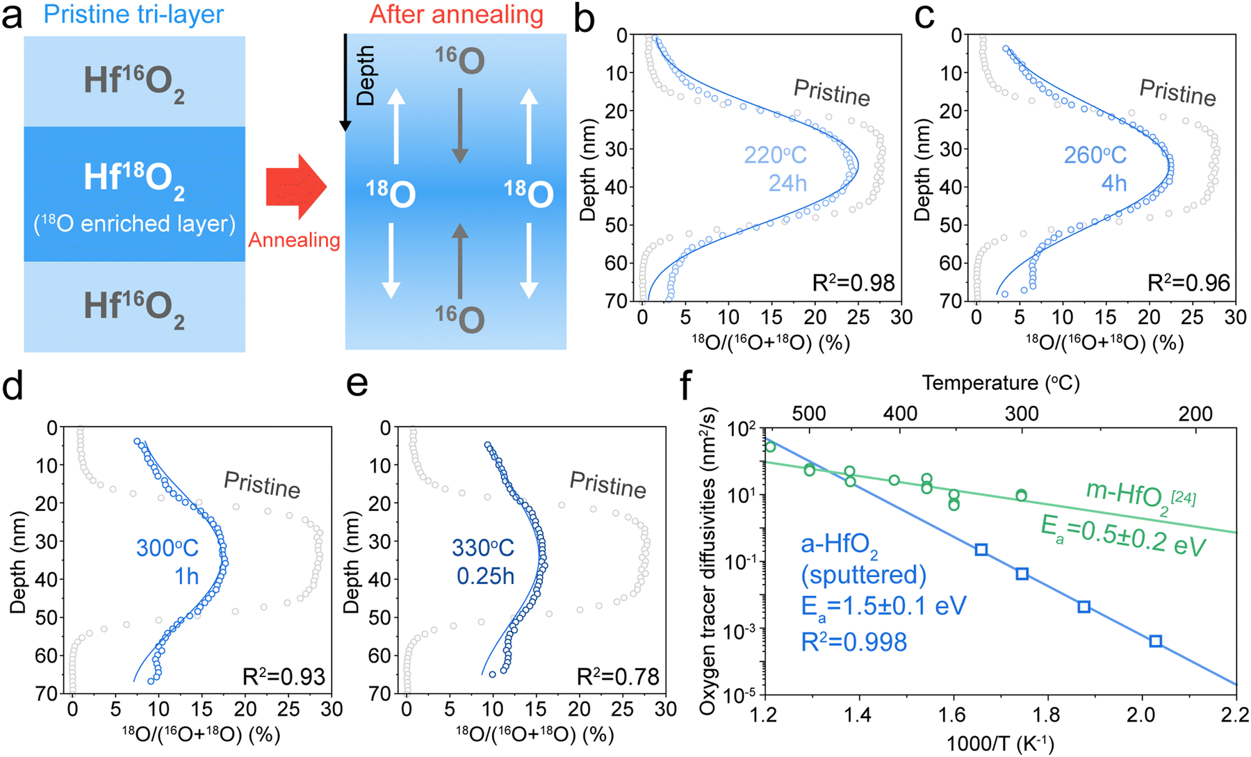 | ||
| Fig. 2 Oxygen tracer diffusivity measurement of sputtered HfO2. (a) Schematic illustration of sample preparation for isotope tracer measurements. The middle layer was enriched with ∼25% 18O (see Experimental methods). (b)–(e) 18O isotope ratios against sample depth at different annealing temperatures and annealing times. ((b) 220 °C 24 h, (c) 260 °C 4 h, (d) 300 °C 1 h, and (e) 330 °C 0.25 h). Grey empty circles represent 18O fraction of samples before annealing (pristine tri-layer samples). Blue empty circles represent 18O fraction of samples after annealing (annealed tri-layer samples). The blue lines in each plot represent the fitting results. (f) Arrhenius plots of oxygen tracer diffusivities: sputtered amorphous HfO2 (a-HfO2, blue empty squares) and monoclinic HfO2 (m-HfO2, green empty circles) from ref. 24. | ||
Fig. 2f shows the Arrhenius plot of oxygen tracer diffusion in sputtered HfO2. The activation energy is 1.5 ± 0.1 eV (2 standard errors). This value is substantially higher than the previously reported activation energy of monoclinic HfO2 (m-HfO2, 0.5 ± 0.2 eV),24 and nearly identical to the 1.4 ± 0.4 eV activation energy from the device retention measurements (Fig. 1e).
We next measure tracer diffusion in ALD-deposited HfO2, which is widely used in resistive memory29,30 and as high-k dielectrics.31,32 Due to the challenges of introducing 18O oxygen into an ALD system, we instead sputter a 15-nm-thick 18O enriched HfO2 above a 20-nm-thick ALD HfO2 film (Fig. 3a). The 18O-enriched film was deposited using the same reactive DC sputtering as used in the sputtered films (Fig. 2a). XRD confirms that both layers are amorphous (Fig. S8, ESI†). XPS shows the two layers are chemically identical (Fig. S9, ESI†). Fig. 3b shows cross-sectional scanning transmission electron microscopy (STEM) images of this sputtered/ALD bi-layer samples. Energy dispersive spectroscopy (EDS) shows that the Hf:O ratio of both films is about 1:2 (Fig. S10, ESI†), but the EDS maps show higher absolute intensity for both Hf and O in the ALD film (Fig. 3c). In Fig. S11 (ESI†), X-ray reflectivity (XRR) analysis shows that ALD HfO2 has a higher density (9.9 g cm−3) than sputtered HfO2 (8.6 g cm−3), which is consistent with the higher Hf and O counts in the STEM-EDS maps (Fig. 3b). While both films are compositionally identical, the ALD films show higher density than the sputtered films.
 | ||
| Fig. 3 Oxygen tracer diffusion measurements for ALD HfO2. (a) Schematic illustration of bi-layer sample preparation for ToF-SIMS depth profiling. (b) STEM-HAADF image of cross sectional pristine bi-layer sample (left) and STEM-EDS mapping images of the bi-layer (mapping of Hf, middle, and O, right) (c). STEM-EDS line scan results. Each curve indicates Hf (blue), and O (red) intensity along the depth of the sample. (d)–(g) ToF-SIMS depth profiling results of annealed samples (red empty circles) and pristine samples (grey empty circles). Red lines show simulated depth. (h) The Arrhenius temperature plots of the measured oxygen diffusion in different types of HfO2. The activation energy of oxygen tracer diffusivities for ALD amorphous HfO2 (a-HfO2) is 1.6 ± 0.3 eV. | ||
Next, we annealed these samples and depth-profiled the oxygen tracer concentrations using ToF-SIMS (Fig. 3d–g). These samples were annealed much longer than the sputtered ones in Fig. 2. While the oxygen tracer profile is relatively uniform in the top sputtered HfO2, it undergoes a sharp gradient in the bottom ALD HfO2. This result qualitatively suggests that the ALD film has much lower oxygen tracer diffusion than the sputtered film. To quantitatively solve for the oxygen diffusivity of the ALD, we use a finite-element simulation using Fick's laws of diffusion that uses the measured “pristine” experimental profile as the initial condition. We use this simulation to solve for the tracer diffusion coefficient that yields the best fit to experimental results (Fig. 3d–g). More details are given in the Experimental methods and in Fig. S12 and S13 (ESI†).
Fig. 3h plots the oxygen tracer diffusion of the ALD HfO2 film alongside that of the sputtered amorphous HfO2 (a-HfO2) and the monoclinic HfO2 (m-HfO2) from ref. 24. The oxygen tracer diffusion activation energy of ALD a-HfO2 was calculated to 1.6 ± 0.3 eV (2 standard errors), which is similar to the activation energy of the sputtered HfO2. However, the absolute magnitude of tracer diffusion in the sputtered HfO2 is about 300 times higher than that of the ALD films. We propose that this 300× difference results from the much lower density of sputtered HfO2 films compared to ALD ones (Fig. 3c, Fig. S10 and S11, ESI†). This result is broadly in agreement with the “free volume” theory of diffusion in amorphous materials, whereby the ion diffusion pathway is enabled by the “free volume” that results from the non-close-packed structure of amorphous materials.33 The difference in density between sputtered a-HfO2 and ALD a-HfO2 may also have produced the slightly different activation energy (1.6 ± 0.3 eV) compared to that of tri-layer sample experiments (1.5 ± 0.1 eV). However, given the confidence interval, we are unable to conclude that these two activation energies are different from one another.
Comparison between oxygen tracer diffusion and device retention measurements
Our oxygen tracer diffusion measurements show that both ALD and sputtered HfO2 have a very similar diffusion activation energy (∼1.5 eV), which is also very similar to the activation energies from the device retention measurements (∼1.4 eV). We next aim to correlate the absolute values between the characteristic diffusion time and the retention time. The characteristic diffusion time τ is given by , where L is the characteristic diffusion length, and DO is the oxygen diffusivity. Fig. 4a displays characteristic diffusion time as a function of the characteristic diffusion length based in ALD a-HfO2 (red), sputtered a-HfO2 (blue), and monoclinic HfO2 (green) at 280 °C.
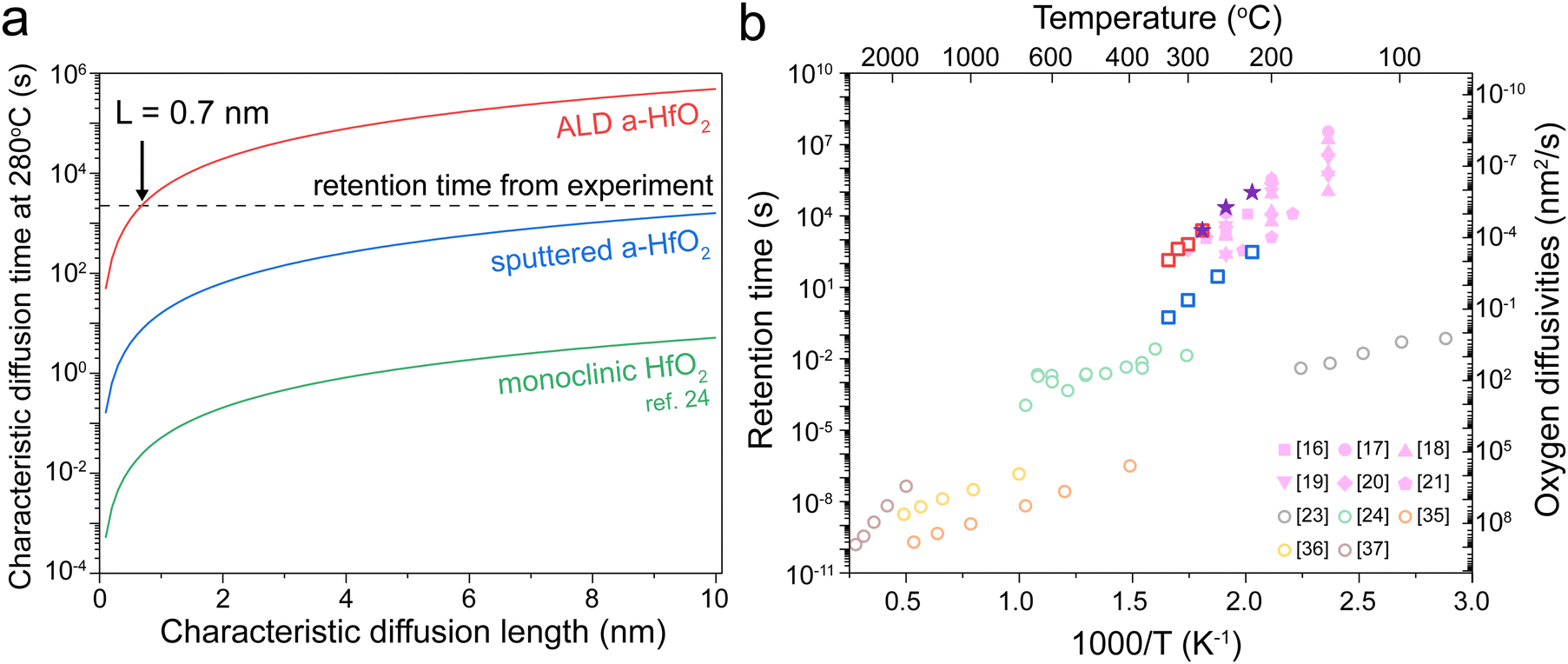 | ||
| Fig. 4 Comparison of retention and diffusion time. (a) The estimated diffusion length for the three types of HfO2 tracer diffusion at 280 °C. The dashed line indicates the experimentally obtained retention failure time. (b) The diffusion time estimates for L = 0.7 nm based on different oxygen diffusion measurements (empty circles), including transient current analysis,23 isotope tracer diffusion,24 and molecular dynamic simulations.35–37 Empty squares: sputtered a-HfO2 (blue) and ALD a-HfO2 (red). The experimentally obtained values for retention failure are given by purple stars (this work) and pink symbols (ref. 16–21). | ||
We next analyze these characteristic diffusion time curves compared with the experimentally measured retention time at 280 °C, designated by the dashed line. Our ALD films intersect at 0.7 nm; this value is very similar to experimentally measured filament diameters of below 5 nm in HfO234 resistive memories. In contrast, the oxygen tracer diffusion of the sputtered film does not intersect until 12 nm, while the value for monoclinic films does not intersect below 200 nm. Based on this result, we believe that the tracer diffusion values in ALD films best represent the oxygen diffusivity in HfO2 resistive memory devices. However, the oxygen diffusivity in a filament may be different than that of a pristine film, which may explain the smaller estimated diffusion length (0.7 nm) compared to the expected filament radius of ∼2 nm for this current compliance.34
Finally, we compare the experimentally measured device retention time with the characteristic oxygen diffusion time obtained from different experimental measurements and computational simulations. Assuming a characteristic diffusion length of 0.7 nm, our results clearly show that the tracer diffusion coefficients obtained in our ALD films best match experimentally obtained retention times in resistive memory devices. Even if the true characteristic diffusion length is not 0.7 nm, our two tracer diffusion measurements are the only experimental results that match the activation energy slope of the resistive memory devices. The isotope tracer measurements offer a more direct approach compared to transient current analysis for measuring oxygen diffusion. Additionally, our work quantified the tracer diffusion in amorphous rather than crystalline HfO2 films, matching the amorphous films used in most HfO2 resistive memory devices.
Discussion
Our results show that the oxygen tracer diffusion of amorphous HfO2 yields an activation energy of ∼1.5 eV, which is qualitatively and quantitatively consistent with experimentally measured device retention times. In contrast, previous experiment work suggests that the activation energy is only ∼0.5 eV,24 which yields many orders of magnitude differences in the predicted retention time. Our work unequivocally suggests that the oxygen diffusion activation energy in amorphous HfO2 is in the ∼1.5 eV range, enabling HfO2 to be a resistive memory with long retention. This work also has important implications for amorphous-HfO2 used in other devices, such as high-k gate dielectrics, or as electrolytes38 or passivation layers39 in electrochemical random-access memory.An important consideration is the difference in the tracer diffusivity mechanisms of a crystalline and an amorphous material. In crystalline materials, the tracer diffusivity is given as the product of the defect (e.g., vacancy or interstitial) concentration and defect diffusivity.40 As a result, the characteristic defect diffusion time is different from the characteristic tracer diffusion time. However, crystallographic point defects cannot be defined in amorphous materials.41 For this reason, we propose that the characteristic oxygen tracer diffusion time offer an appropriate metric for estimating the device retention time. As we show, the film density plays a large role in the oxygen tracer diffusivity.
It was recently shown that oxygen may undergo “uphill” diffusion against the concentration gradient because of spinodal decomposition.26 However, these devices would fail from the high-resistance to the low-resistance state. Our results show device failure from the low-resistance to the high-resistance state (Fig. 1) under our current compliance, which implies that the filaments dissolve over time. While our characteristic diffusion time model does not incorporate the thermodynamic factor, this thermodynamic factor is likely only a small correction to the diffusion time. Our work further assumes that oxygen diffusion in the suboxides that make up a filament is similar to oxygen diffusion in stoichiometric HfO2 films. Preliminary investigation of oxygen diffusion in sputtered sub-stoichiometric HfO1.2 shows an activation energy ∼1.2 ± 0.4 eV, but an absolute magnitude similar to that of ALD films (Fig. S9 and S14, ESI†). The slight difference in the device retention activation energy and the tracer diffusion measurements may be because the devices contain a suboxide filament. The oxygen diffusivity of this suboxide, which may even be crystalline,10 is likely different from that of an amorphous film deposited by sputtering or ALD. However, the overall range of the activation energies between our oxygen tracer diffusion (1.2–1.6 eV) and the device retention time (∼1.4 ± 0.4 eV) shows that our results are much closer to the oxygen diffusion in Hafnia resistive memory devices, as opposed to previous measurements showing ∼0.5 eV activation energy.
Conclusion
In this work, we conducted the first oxygen tracer diffusion measurements in amorphous HfO2, a technologically important material for resistive memory and high-k dielectrics. Our results show that the oxygen tracer diffusion is much lower than those measured using other methods, and qualitatively matches the retention times in HfO2 resistive memory devices. Furthermore, our results show that the oxygen tracer diffusion in less-dense sputtered films is about 300 times higher than that of denser films deposited by atomic layer deposition, despite nominally identical chemical compositions. The oxygen tracer diffusion in atomic layer deposited films yield characteristic diffusion times that much more closely match the retention times in HfO2 resistive memory devices.Experimental methods
HfO2 resistive memory fabrication
The characterized HfO2 resistive memory was fabricated at the Albany NanoTech Complex by NY CREATES and the College of Nanotechnology, Science & Engineering (University at Albany). The devices are fabricated on a 300 mm wafer using a 65 nm back end of line (BEOL) process technology with custom modules embedding the resistive memory elements between tungsten and copper metallization 1 and 2, respectively (W-M1 and Cu-M2). The W-M1 interconnect is utilized to fabricate in-line resistors with 10 kΩ enabling on-chip current overshoot control during the resistive memory forming process. An inert TiN bottom electrode (BE) was structured above the W-M1 layer with a device diameter of 80 nm. The fabrication of the BE module was finished by a chemical mechanical polishing (CMP) process leaving an atomically flat contact for the deposition of the resistive memory stack. The 5.8 nm HfO2 switching layer (SL) was deposited via atomic layer deposition (ALD) and followed by 6 and 40 nm of Ti and TiN via sputtering, which serves as the oxygen exchange layer (OEL) and top electrode (TE), respectively. The resistive memory stack was structured via a reactive ion etch (RIE) process to isolate the devices and an overlay of the SL, OEL, and TE above the BE of around 50 nm is maintained to avoid RIE edge effects during filament formation. The connection to the TE and Cu-M2 layer was accomplished using a via-first dual damascene process where the via etch and hard mask thickness are tuned to enable the bridging of the vertical height difference to connect the TiN top electrode and the Cu-M2 with a single patterning process. More details are given in our previous work.42–47Electrical measurements
The HfO2 resistive memories were measured with Keithley 4200 semiconductor parameter analyzer. For DC switching measurements, the voltage bias was applied on the top electrode with the bottom electrode grounded. The current compliance was set at 100 μA. For the forming step, a voltage sweep was conducted up to 4 V, and, continuously, 20 cycles of RESET and SET cycles were applied with −2 V and 2 V DC sweep, respectively. One representative switching behavior of HfO2 resistive memory is displayed in Fig. 1c.In Fig. S3 (ESI†), we measured retention after 1000 cycles of pulse switching. Each cycle was composed of the following steps: RESET voltage was set to −3 V, and SET voltage was set to 2 V. To read the resistance value of the device after RESET and SET operations, we included reading steps with a voltage of 0.15 V. All pulse widths were fixed to 20 μs, and current compliance was set as 10 μA. Fig. S3 (ESI†) a displays a typical switching result of the pulsed switching.
After finishing switching cycles (DC or pulsed), the resistive switching devices were annealed under different temperatures (220 °C, 250 °C, and 280 °C) for retention measurement. The annealing was conducted in a temperature and environmentally controlled probe station (Everbeing CG-196) under ∼300 Torr of Ar. The conductance measurement was performed after cooling the memory devices at room temperature using voltage sweeps up to 0.1 V using the Keithley 4200.
Oxygen tracer diffusion measurement
Tri-layer (Hf16O2/Hf18O2/Hf16O2) samples were deposited by using DC reactive sputtering using a 76-mm Hf metal target (AJA International Inc, 99.9% purity) via AJA Orion-8 Sputter System with three mass flow controllers. We used 100 W of sputter power while flowing 4 sccm of O2 and 36 sccm of Ar under a total gas pressure of 5 mTorr. For the natural-abundance layer (Hf16O2), we used a standard 99.999% purity O2 cylinder with the natural O2 abundance (∼99.8% 16O2). For the 18O isotope enriched layer (Hf18O2), the O2 gas consisted of 1 sccm of 99%-enriched 18O2 (Sigma-Aldrich, 99.9% purity) and 3 sccm of the natural abundance O2 gas. Lastly, a 25 nm Pt layer was deposited on top of the tri-layer to prevent further oxidation under air. The prepared tri-layer samples were annealed under each condition under flowing inert Ar (∼100 sccm) for 220 °C 24 hours, 260 °C 4 hours, 300 °C 1 hour, and 330 °C 0.25 hours using a Nextron CHH750 environmental probe station. The oxygen partial pressure of the chamber was measured to be around 3 × 10⁻⁶ bar using a Zirox ZR5 oxygen sensor.Bi-layer (Hf18O2/Hf16O2) samples were prepared via atomic layer deposition (ALD) for the bottom layer (natural abundance) and reactive sputter deposition for the top layer (isotope-enriched). The bottom ALD layer was deposited with the Veeco Fiji ALD system in the Lurie Nanofabrication Facility (LNF) at the University of Michigan. Thermal ALD (200 °C) was conducted for the bottom layer with precursor (tetrakis(dimethylamino)hafnium, TDMAH). Subsequently, the 18O-enriched top layer was deposited with the same procedure as the enriched layer in the previous paragraph. The 60 nm protective Pt layer was sputtered to reduce oxidation under air. The prepared bi-layer samples were annealed with each condition (280 °C 18 hours, 300 °C 9 hours, 315 °C 5 hours, and 330 °C 2 hours) under flowing Ar (∼100 sccm) in the Nextron environmental probe station.
The time-of-flight secondary ion mass spectrometry (ToF-SIMS) analysis was performed using the ToF.SIMS.5-NSC instrument (ION.TOF GmbH) at the Center for Nanophase Materials Sciences at Oak Ridge National Laboratory. A Bi3+ liquid metal ion gun, operating at 30 keV energy, 0.5 nA current (DC mode), and with a spot size of approximately 120 nm, served as the primary source for chemical analysis. A Cs+ sputter ion gun was additionally used with operating at 1 keV energy and 70 nA current for depth profiling. The measurements were conducted in non-interlaced mode, with each analysis scan by Bi3+ (100 × 100 μm2) was succeeded by 2 seconds of sputtering with Cs+ (300 × 300 μm2). Low energy electron flood gun was used for charge compensation. Secondary ions were then analyzed using time-of-flight mass analyzers with a mass resolution of m/Δm = 100–300 in the negative ion detection mode. Intensities of the peaks corresponding to 16O− and 18O− ions were further analyzed to calculate 18O/(16O + 18O) ratio.
Materials characterization
Scanning transmission electron microscope (STEM) measurements were taken using a Thermo Fisher Talos F200X G2 at the University of Michigan. A 200 kV field emission gun (FEG) scanning transmission electron microscope operated. The Velox software was used for STEM images and energy-dispersive X-ray spectroscopy (EDS) data acquisitions. The TEM specimen was prepared using a Thermo-Fisher Helios 650 Xe Plasma Focused Ion Beam (FIB). The final beam condition was set at 12 keV and 10 pA for the polishing of the specimen.X-ray diffraction (XRD) and X-ray reflectivity (XRR) measurements were conducted using a Rigaku Smartlab X-ray diffractometer using a Cu K-α source. For XRD measurement, annealed bi-layer samples and annealed tri-layer samples were used. A 20 nm layer of sputtered and ALD HfO2 film were used for XRR density measurements.
X-ray photoelectron spectroscopy (XPS) was performed using Kratos Axis Ultra XPS system with a monochromatic Al source at room temperature.
Data fitting
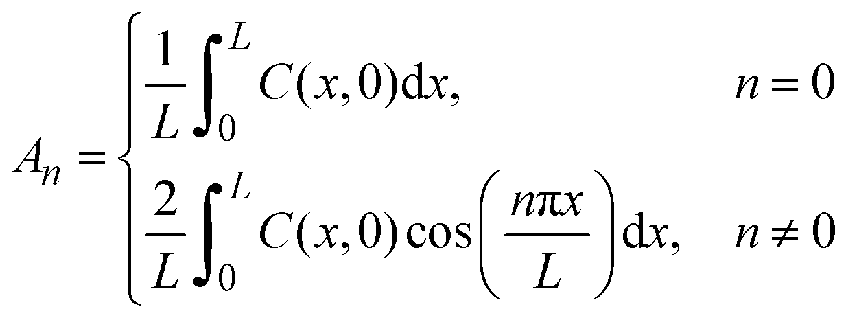
We used Crank's approach to solve for Fick's law of diffusion based on a separation of variables, with a zero-flux boundary condition:
x is depth of samples, and L represents tri-layer sample thickness (∼70 nm). We used the ToF-SIMS profile of the “pristine” sample as the initial condition; in this manner, we can account for the diffusion that occurs at room temperature between the sample fabrication and the ToF-SIMS measurements, around 10 days. Our solution is based on a Fourier Series decomposition of this “initial” condition, using the following analytical solutions:
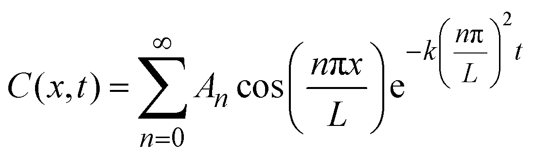
where the “initial condition” C(x,0) is the results of the experimentally-measured “pristine” film.
These analytical solutions provide good fits to the ToF-SIMS results of the sputtered samples (Fig. 2), where the oxygen diffusion D is nominally uniform across the sputtered tri-layer films, which are chemically identical. However, this solution would not be applicable for the bi-layer films because the oxygen diffusion of the sputtered and ALD films is different.
To solve this problem, we used finite element methods with COMSOL Multiphysics 6.1, Transport of Dilute Species Module, to fit concentration profiles of bi-layer samples. This simulation contains two layers: the top sputtered layer uses the oxygen tracer diffusivities from the analytical solutions (Fig. 2), while the diffusivity of the ALD layer was fitted. We again use the measured concentration profiles of the “pristine” bi-layer samples as the initial condition.
Next, we simulated the concentration profile for each annealing condition and compared the simulated oxygen tracer profile with the experimental oxygen tracer profiles under the same annealing condition (Fig. S12, ESI†). We then computed the coefficient of determination (R2) as a function of the fitted ALD diffusion values. The optimal oxygen tracer diffusivity is the one with the highest R2 (Fig. S13, ESI†).
Data availability
The data for the work can be accessed in the Materials Commons 2.0 Archive: https://doi.org/10.13011/m3-e9jr-6g69. Any additional data (raw or processed) can be obtained upon reasonable request to the corresponding author.Author contributions
K. B. and N. C. developed and fabricated the memristor devices. D. S., J. L. and P. R. collected the memristor device data. J. L. conducted the TEM. D. S. and J. L. conducted the thin film sample deposition. D. S. analyzed and fitted the data. A. V. I. conducted the ToF-SIMS analysis. Y. L. supervised the project. All authors contributed to writing, revising, and/or editing of the manuscript.Conflicts of interest
The authors declare no financial conflicts of interest.Acknowledgements
The work at the University of Michigan was supported by the National Science Foundation under Grant no. ECCS-2106225 and startup funding from the University of Michigan College of Engineering. Y. L. acknowledges the support of an Intel Rising Star Gift. A. V. I. was partly supported by the DOE Office of Science Research Program for Microelectronics Codesign (sponsored by ASCR, BES, HEP, NP, and FES) through the Abisko Project, PM Robinson Pino (ASCR). The work at the State University of New York, University at Albany and NY CREATES was supported by the Air Force Research Laboratory under agreement numbers FA8750-21-1-1018 and FA8750-21-1-1019. The U.S. Government may reproduce and distribute reprints for Governmental purposes, despite any copyright notation. The views and conclusions expressed herein are solely those of the authors and do not necessarily reflect the official policies or endorsements of the Air Force Research Laboratory or the U.S. Government. The ToF-SIMS measurements were conducted at the Center for Nanophase Materials Sciences, which is a DOE Office of Science User Facility, and using instrumentation within ORNL's Materials Characterization Core provided by UT-Battelle, LLC under Contract No. DE-AC05-00OR22725 with the U.S. Department of Energy. The authors acknowledge Wei D. Lu (University of Michigan), Yang Zhang (University of Michigan), A. Alec Talin (Sandia National Laboratories), Jonathan Ihlefeld (University of Virginia), Nicole Thomas (Intel), and Seung Hoon Sung (Intel) for helpful discussions on this research. The authors acknowledge the financial support from the University of Michigan College of Engineering and NSF grant no. DMR-0420785, and technical support from the Michigan Center for Materials Characterization. Atomic laser deposition was conducted at the University of Michigan, Lurie Nanofabrication Facility.References
- M. Lanza, A. Sebastian, W. D. Lu, M. Le Gallo, M.-F. Chang, D. Akinwande, F. M. Puglisi, H. N. Alshareef, M. Liu and J. B. Roldan, Science, 2022, 376, eabj9979 CrossRef CAS PubMed.
- J. J. Yang, D. B. Strukov and D. R. Stewart, Nat. Nanotechnol., 2013, 8, 13–24 CrossRef CAS PubMed.
- D. Ielmini and H.-S. P. Wong, Nat. Electron., 2018, 1, 333–343 CrossRef.
- Q. Xia and J. J. Yang, Nat. Mater., 2019, 18, 309–323 CrossRef CAS PubMed.
- Z. Wang, H. Wu, G. W. Burr, C. S. Hwang, K. L. Wang, Q. Xia and J. J. Yang, Nat. Rev. Mater., 2020, 5, 173–195 CrossRef CAS.
- R. Dittmann, S. Menzel and R. Waser, Adv. Phys., 2021, 70, 155–349 CrossRef.
- R. Waser, R. Dittmann, G. Staikov and K. Szot, Adv. Mater., 2009, 21, 2632–2663 CrossRef CAS PubMed.
- D.-H. Kwon, K. M. Kim, J. H. Jang, J. M. Jeon, M. H. Lee, G. H. Kim, X.-S. Li, G.-S. Park, B. Lee, S. Han, M. Kim and C. S. Hwang, Nat. Nanotechnol., 2010, 5, 148–153 CrossRef CAS PubMed.
- Y. Yang, X. Zhang, L. Qin, Q. Zeng, X. Qiu and R. Huang, Nat. Commun., 2017, 8, 15173 CrossRef PubMed.
- Y. Zhang, G.-Q. Mao, X. Zhao, Y. Li, M. Zhang, Z. Wu, W. Wu, H. Sun, Y. Guo, L. Wang, X. Zhang, Q. Liu, H. Lv, K.-H. Xue, G. Xu, X. Miao, S. Long and M. Liu, Nat. Commun., 2021, 12, 7232 CrossRef CAS PubMed.
- W. Banerjee, A. Kashir and S. Kamba, Small, 2022, 18, 2107575 CrossRef CAS PubMed.
- M. Lanza, H.-S. P. Wong, E. Pop, D. Ielmini, D. Strukov, B. C. Regan, L. Larcher, M. A. Villena, J. J. Yang, L. Goux, A. Belmonte, Y. Yang, F. M. Puglisi, J. Kang, B. Magyari-Köpe, E. Yalon, A. Kenyon, M. Buckwell, A. Mehonic, A. Shluger, H. Li, T. Hou, B. Hudec, D. Akinwande, R. Ge, S. Ambrogio, J. B. Roldan, E. Miranda, J. Suñe, K. L. Pey, X. Wu, N. Raghavan, E. Wu, W. D. Lu, G. Navarro, W. Zhang, H. Wu, R. Li, A. Holleitner, U. Wurstbauer, M. C. Lemme, M. Liu, S. Long, Q. Liu, H. Lv, A. Padovani, P. Pavan, I. Valov, X. Jing, T. Han, K. Zhu, S. Chen, F. Hui and Y. Shi, Adv. Electron. Mater., 2019, 5, 1800143 CrossRef.
- S. Larentis, C. Cagli, F. Nardi and D. Ielmini, Microelectron. Eng., 2011, 88, 1119–1123 CrossRef CAS.
- S. Choi, J. Lee, S. Kim and W. D. Lu, Appl. Phys. Lett., 2014, 105, 113510 CrossRef.
- Resistive switching: from fundamentals of nanoionic redox processes to memristive device applications, ed. D. Ielmini and R. Waser, Wiley-VCH Verlag GmbH & Co. KGaA, Weinheim, 2016 Search PubMed.
- M. Azzaz, E. Vianello, B. Sklenard, P. Blaise, A. Roule, C. Sabbione, S. Bernasconi, C. Charpin, C. Cagli, E. Jalaguier, S. Jeannot, S. Denorme, P. Candelier, M. Yu, L. Nistor, C. Fenouillet-Beranger and L. Perniola, 2016 IEEE 8th International Memory Workshop (IMW), IEEE, Paris, France, 2016, pp. 1–4 Search PubMed.
- Y. Y. Chen, M. Komura, R. Degraeve, B. Govoreanu, L. Goux, A. Fantini, N. Raghavan, S. Clima, L. Zhang, A. Belmonte, A. Redolfi, G. S. Kar, G. Groeseneken, D. J. Wouters and M. Jurczak, 2013 IEEE International Electron Devices Meeting, IEEE, Washington, DC, USA, 2013, pp. 10.1.1–10.1.4 Search PubMed.
- Y. Y. Chen, L. Goux, S. Clima, B. Govoreanu, R. Degraeve, G. S. Kar, A. Fantini, G. Groeseneken, D. J. Wouters and M. Jurczak, IEEE Trans. Electron Devices, 2013, 60, 1114–1121 CAS.
- Y. Y. Chen, R. Degraeve, S. Clima, B. Govoreanu, L. Goux, A. Fantini, G. S. Kar, G. Pourtois, G. Groeseneken, D. J. Wouters and M. Jurczak, 2012 International Electron Devices Meeting, IEEE, San Francisco, CA, USA, 2012, pp. 20.3.1–20.3.4 Search PubMed.
- B. Traore, P. Blaise, E. Vianello, H. Grampeix, S. Jeannot, L. Perniola, B. De Salvo and Y. Nishi, IEEE Trans. Electron Devices, 2015, 62, 4029–4036 Search PubMed.
- M. Zhao, H. Wu, B. Gao, Q. Zhang, W. Wu, S. Wang, Y. Xi, D. Wu, N. Deng, S. Yu, H.-Y. Chen and H. Qian, 2017 IEEE International Electron Devices Meeting (IEDM), IEEE, San Francisco, CA, USA, 2017, pp. 39.4.1–39.4.4 Search PubMed.
- Z. Wei, T. Takagi, Y. Kanzawa, Y. Katoh, T. Ninomiya, K. Kawai, S. Muraoka, S. Mitani, K. Katayama, S. Fujii, R. Miyanaga, Y. Kawashima, T. Mikawa, K. Shimakawa and K. Aono, 2011 International Electron Devices Meeting, IEEE, Washington, DC, USA, 2011, pp. 31.4.1–31.4.4 Search PubMed.
- S. Zafar, H. Jagannathan, L. F. Edge and D. Gupta, Appl. Phys. Lett., 2011, 98, 152903 CrossRef.
- M. P. Mueller and R. A. De Souza, Appl. Phys. Lett., 2018, 112, 051908 CrossRef.
- Y.-F. Chang, J. A. O’Donnell, T. Acosta, R. Kotlyar, A. Chen, P. A. Quintero, N. Strutt, O. Golonzka, C. Connor and J. Hicks, 2020 IEEE International Reliability Physics Symposium (IRPS), IEEE, Dallas, TX, USA, 2020, pp. 1–4 DOI:10.1109/IRPS45951.2020.9128359.
- J. Li, A. Appachar, S. Peczonczyk, E. Harrison, B. Roest, A. Ievlev, R. Hood, S. Yoo, K. Sun, A. Talin, W. Lu, S. Kumar, W. Sun and Y. Li, Thermodynamic origin of nonvolatility in resistive switching, 2022 DOI:10.21203/rs.3.rs-2365752/v1.
- R. A. De Souza and M. Martin, Phys. Status Solidi C, 2007, 4, 1785–1801 CrossRef CAS.
- J. Crank, The mathematics of diffusion, Univ. Pr, Oxford, 2nd edn, repr., 2011 Search PubMed.
- H. Kim, H.-B.-R. Lee and W.-J. Maeng, Thin Solid Films, 2009, 517, 2563–2580 CrossRef CAS.
- A. S. Sokolov, Y.-R. Jeon, S. Kim, B. Ku, D. Lim, H. Han, M. G. Chae, J. Lee, B. G. Ha and C. Choi, Appl. Surf. Sci., 2018, 434, 822–830 CrossRef CAS.
- K. Mistry, R. Chau, C.-H. Choi, G. Ding, K. Fischer, T. Ghani, R. Grover, W. Han, D. Hanken, M. Hattendorf, J. He, C. Allen, J. Hicks, R. Huessner, D. Ingerly, P. Jain, R. James, L. Jong, S. Joshi, C. Kenyon, K. Kuhn, K. Lee, C. Auth, H. Liu, J. Maiz, B. McIntyre, P. Moon, J. Neirynck, S. Pae, C. Parker, D. Parsons, C. Prasad, L. Pipes, B. Beattie, M. Prince, P. Ranade, T. Reynolds, J. Sandford, L. Shifren, J. Sebastian, J. Seiple, D. Simon, S. Sivakumar, P. Smith, D. Bergstrom, C. Thomas, T. Troeger, P. Vandervoorn, S. Williams, K. Zawadzki, M. Bost, M. Brazier, M. Buehler and A. Cappellani, 2007 IEEE International Electron Devices Meeting, IEEE, Washington, DC, 2007, pp. 247–250 DOI:10.1109/IEDM.2007.4418914.
- J. H. Choi, Y. Mao and J. P. Chang, Mater. Sci. Eng., R, 2011, 72, 97–136 CrossRef.
- F. Faupel, W. Frank, M.-P. Macht, H. Mehrer, V. Naundorf, K. Rätzke, H. R. Schober, S. K. Sharma and H. Teichler, Rev. Mod. Phys., 2003, 75, 237–280 CrossRef.
- U. Celano, L. Goux, R. Degraeve, A. Fantini, O. Richard, H. Bender, M. Jurczak and W. Vandervorst, Nano Lett., 2015, 15, 7970–7975 CrossRef CAS PubMed.
- S. Clima, Y. Y. Chen, R. Degraeve, M. Mees, K. Sankaran, B. Govoreanu, M. Jurczak, S. De Gendt and G. Pourtois, Appl. Phys. Lett., 2012, 100, 133102 CrossRef.
- M. Schie, M. P. Müller, M. Salinga, R. Waser and R. A. De Souza, J. Chem. Phys., 2017, 146, 094508 CrossRef.
- G. Broglia, G. Ori, L. Larcher and M. Montorsi, Modell. Simul. Mater. Sci. Eng., 2014, 22, 065006 CrossRef CAS.
- S. Kim, T. Todorov, M. Onen, T. Gokmen, D. Bishop, P. Solomon, K.-T. Lee, M. Copel, D. B. Farmer, J. A. Ott, T. Ando, H. Miyazoe, V. Narayanan and J. Rozen, 2019 IEEE International Electron Devices Meeting (IEDM), IEEE, San Francisco, CA, USA, 2019, pp. 35.7.1–35.7.4 Search PubMed.
- D. S. Kim, V. J. Watkins, L. A. Cline, J. Li, K. Sun, J. D. Sugar, E. J. Fuller, A. A. Talin and Y. Li, Adv. Electron. Mater., 2023, 9(1), 2200958 CrossRef CAS.
- R. A. De Souza, Adv. Funct. Mater., 2015, 25, 6326–6342 CrossRef CAS.
- R. De Souza and G. Harrington, Nat. Mater., 2023, 22, 794–797 CrossRef CAS PubMed.
- M. Liehr, K. Beckmann and N. Cady, 2022 IEEE 31st Microelectronics Design & Test Symposium (MDTS), IEEE, Albany, NY, USA, 2022, pp. 1–6 DOI:10.1109/MDTS54894.2022.9826924.
- M. Abedin, N. Gong, K. Beckmann, M. Liehr, I. Saraf, O. Van Der Straten, T. Ando and N. Cady, Sci. Rep., 2023, 13, 14963 CrossRef CAS PubMed.
- J. Hazra, M. Liehr, K. Beckmann, M. Abedin, S. Rafq and N. Cady, 2021 IEEE International Memory Workshop (IMW), IEEE, Dresden, Germany, 2021, pp. 1–4 DOI:10.1109/IMW51353.2021.9439618.
- K. Beckmann, W. Olin-Ammentorp, G. Chakma, S. Amer, G. S. Rose, C. Hobbs, J. V. Nostrand, M. Rodgers and N. C. Cady, J. Emerg. Technol. Comput. Syst., 2020, 16(2), 23 Search PubMed.
- K. Beckmann, N. Suguitan, J. Van Nostrand and N. C. Cady, Semicond. Sci. Technol., 2019, 34, 105021 CrossRef CAS.
- K. Beckmann, J. Holt, W. Olin-Ammentorp, Z. Alamgir, J. Van Nostrand and N. C. Cady, Semicond. Sci. Technol., 2017, 32, 095013 CrossRef.
Footnote |
| † Electronic supplementary information (ESI) available. See DOI: https://doi.org/10.1039/d3mh02113k |
| This journal is © The Royal Society of Chemistry 2024 |