
 Open Access Article
 This Open Access Article is licensed under a Creative Commons Attribution-Non Commercial 3.0 Unported Licence
Profound influence of surface trap states on the utilization of charge carriers in CdS photoanodes†
Elif Öykü
Alagöz
ab,
Hadi
Jahangiri
c and
Sarp
Kaya
 *ab
*ab
aDepartment of Chemistry, Koç University, 34450 Istanbul, Turkey. E-mail: sarpkaya@ku.edu.tr
bKoç University Tüpraş Energy Center (KUTEM), 34450 Istanbul, Turkey
cKoç University Surface Science and Technology Center (KUYTAM), 34450 Istanbul, Turkey
First published on 5th December 2023
Abstract
CdS is one of the most promising photoanode candidates for photoelectrochemical (PEC) water splitting because of its narrow bandgap, suitable band-edge alignment, and facile fabrication. However, it suffers from photocorrosion and instability due to surface charge recombination. Extensive PEC characterization studies showed that hole utilization at the photoanode/electrolyte interface is the bottleneck for CdS photoanodes. In this study, the fundamental charge carrier dynamics processes on CdS surfaces were investigated and a deactivation mechanism was proposed where surface sulfur vacancies (Sv) served as electron trap centers that caused surface charge recombination. Detailed photocurrent transients showed that the extent of trapping was affected by Sv content and oxygen evolution via the water oxidation reaction. To circumvent this issue, a surface decoration method was demonstrated by using hexadecyltrimethylammonium bromide (CTAB) which passivated electron trapping via occupation of the surface Svs by Br−. This work may contribute to further studies on CdS and other semiconductor photoelectrodes to enhance the understanding of charge utilization processes at photoanode–electrolyte interfaces.
Introduction
Photoelectrochemical conversion (PEC) by splitting water using semiconductor materials is one of the most promising clean energy technologies as a facile and effective strategy for converting solar energy into green hydrogen. Transition metal chalcogenides such as CdS, MoS2, WS2, and CdSe have attracted a great deal of attention with their significant potential and unique properties.1–3 Among all, CdS is an excellent choice owing to its superior qualities, such as appropriate band positioning, narrow band-gap energy, and efficient visible light absorption characteristics.4 Despite the advantages, its widespread utilization is still limited by poor charge separation and instability issues due to photocorrosion and surface charge recombination, which results in activity loss.5 There have been several attempts to enhance the oxygen evolution reaction (OER) efficiency and photo-stability of CdS, such as building heterojunction structures with other semiconductors to improve hole extraction,6–8 using OER co-catalysts for better charge utilization at the photoanode–electrolyte interface,9–11 and modification of the photoanode surface with passivation overlayers to prevent photocorrosion.12,13 Although such surface engineering strategies can increase the photocurrent densities and boost the OER kinetics, the photostability issues, and the fundamental understanding of the charge transfer and utilization mechanisms remain a matter of debate.In addition to these possible solutions, it has been reported that the controlled growth of semiconductors with the help of surface-active reagents can also have an impact on their photocatalytic and PEC activities.14,15 Surfactants such as polyethylene glycol (PEG), sodium dodecyl sulfide (SDS), thioglycerol (TG), and hexadecyltrimethylammonium bromide (CTAB) are used as stabilizing reagents in order to control the direction and the extent of the particle growth and to manipulate the optical and structural characteristics of the nanomaterials.16–18 In comparison to other surfactants, CTAB is less toxic and cheaper as a capping agent alternative which is significantly utilized for the synthesis of CdS colloidal particles. It is a cationic surfactant consisting of a hydrophobic tail and a positively charged ammonium (NH4) head group with bromide anion (Br−).19 Although it shows promising results for the synthesis of photocatalysts and is extensively studied in the literature as a simple option to manipulate photocatalytic behavior, its potential as an overlayer is not promoted enough. Li et al.20 used CTAB on Fe2O3 photoanode by a hydrothermal deposition method followed by a post-annealing treatment. They reported impressive results for photocurrent density increase and enhanced charge separation. They proposed a working mechanism where Br− of CTAB acts like a redox mediator at the photoanode–electrolyte interface. They supported this hypothesis by transient photocurrent (TPC) and electrochemical impedance spectroscopy (EIS) where the photocurrent density of pristine Fe2O3 showed a significant increase and a lower charge transfer resistance. A different approach was reported by Sun et al.21 where they designed a 2D WSe2 p–n junction by electron doping with CTAB. They conducted computational studies on both WSe2 and WS2 to study the adsorption behavior of CTAB on transition metal dichalcogenides. Their calculations showed that the carrier density of CTAB treated WS2 was higher than that of pristine one and they attributed this result to the sulfur vacancy (Sv) sites occupied by Br− which acted like an electron dopant to give p-type characteristic to the junction structure.
Herein, we aim to discuss the potential-dependent charge transfer and utilization properties of the CdS and CTAB decorated CdS photoanodes by probing the transient behavior with linear sweep voltammetry (LSV) under chopped illumination to investigate the obstacles for PEC efficiency. Results demonstrate that CTAB has a positive effect on inhibiting hole accumulation by acting like a hole-collecting layer on the surface. Several PEC and structural characterization techniques were applied to propose an adsorption mechanism for CTAB. We studied the surface reaction kinetics of CdS by in situ photoluminescence (PL), EIS, and TPC measurements to provide a detailed analysis of the reactions taking place at the photoanode–electrolyte interface and how these reactions affect the OER efficiency.
Results and discussion
Surfactant-free hydrothermal synthesis of CdS photoanodes and modification of the CdS surface with CTAB after the synthesis by dip-coating method was successfully performed. Dip-coating time of CdS/FTO photoanodes was set as 2 and 6 h to see how the amount of CTAB overlayer changes with dip-coating time. The successful deposition of CdS and CTAB was investigated by X-ray photoelectron spectroscopy (XPS), Fourier transform infrared (FTIR) analysis, and high-resolution transmission electron microscopy (HRTEM) imaging, which is shown in Fig. 1.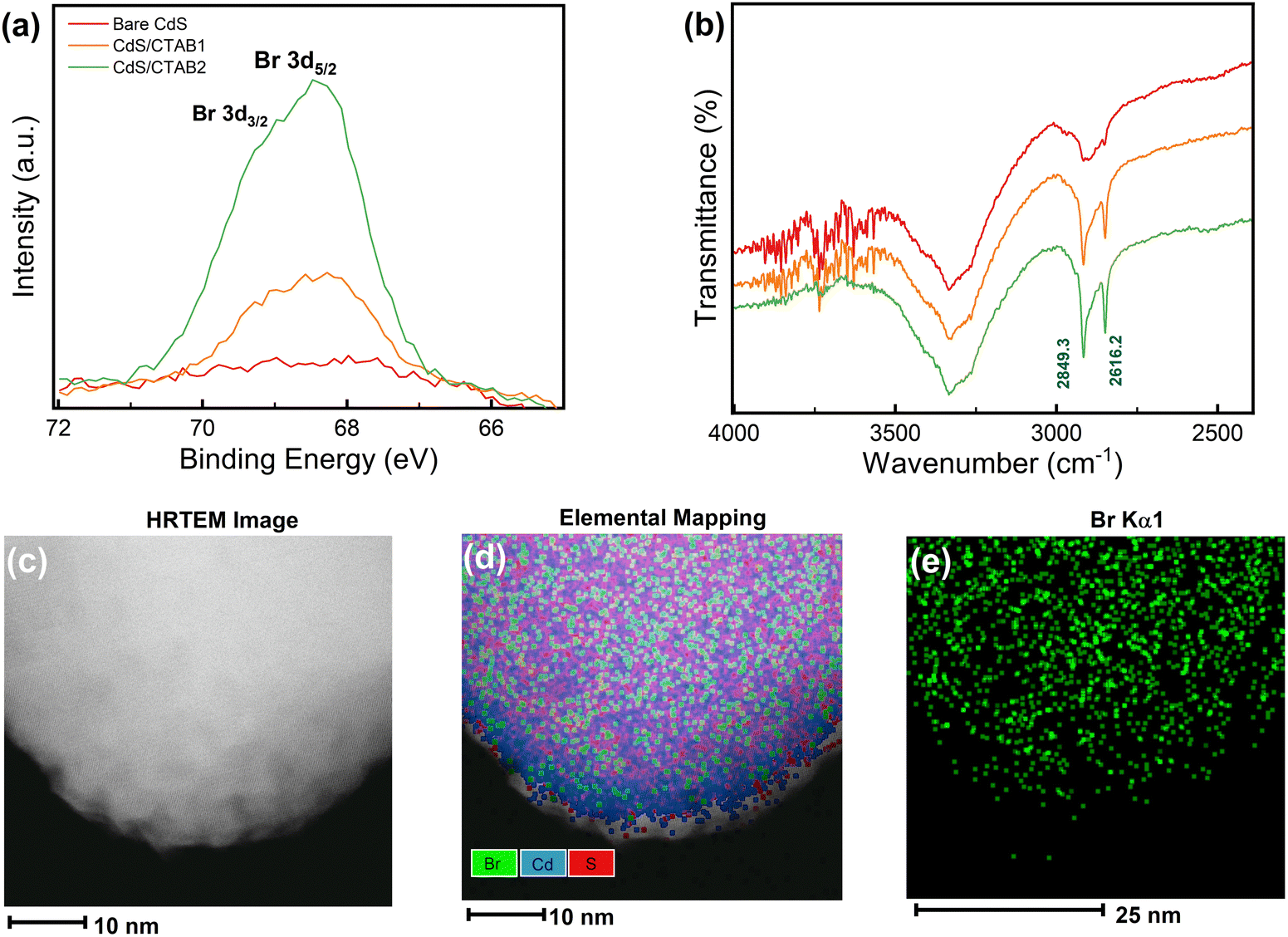 | ||
| Fig. 1 (a) Br 3d XPS spectra, and (b) FTIR spectra of bare CdS, CdS/CTAB1, and CdS/CTAB2. (c) HRTEM image of CdS/CTAB2 powder sample, (d) EDX elemental mapping of Br, Cd, and S, and (e) Br Kα1 elemental mapping. | ||
The control over the CTAB overlayer growth is verified by the Br 3d XPS spectra in Fig. 1a where the intensity of the Br 3d peak located at 68.3 eV22 increases with longer dip-coating time. The atomic percent of Br was calculated as 10.5% after 2 h, and 22.4% after 6 h of dip-coating. The photoanode with lower and higher atomic percentages of Br will be denoted as CdS/CTAB1 and CdS/CTAB2, respectively. Fig. S1a and b (ESI†) demonstrate Cd 3d and S 2p XPS spectra of bare CdS after hydrothermal deposition and the effect of CTAB adsorption on their intensities. The spin–orbit split Cd 3d peaks at 411.8 eV (Cd 3d5/2) and 405.3 eV (Cd 3d5/2) and S 2p peaks at 162.6 eV (S 2p3/2) and 161.4 eV (S 2p1/2) confirm the stoichiometric CdS formation. In addition to the evolution of Br 3d peaks, the gradual decrease in Cd 3d and S 2p peak intensities also shows the presence of the CTAB overlayer on the CdS surface.23
The increase in C 1s peak intensity presented in Fig. S1c (ESI†) and the appearance of symmetric and asymmetric C–H stretching bands at 2616.2 and 2849.3 cm−1 in Fig. 1b show the presence of the hydrophobic tail of CTAB.24 It can be anticipated that CTAB is adsorbed on the CdS surface together with Br− and hydrophobic tail. It is known that CdS is sensitive to surface oxidation even if it is kept in the dark. The peak located at 168.4 eV in S 2p spectrum must be considered to investigate the effect of CTAB on the surface oxidation of CdS. This peak is attributed to SO42− which is an oxidation product of S2− on the surface.25,26
The homogeneity of surface coverage by CTAB is further confirmed by HRTEM and elemental mapping done by energy dispersive X-ray spectroscopy (EDX). HRTEM image, the elemental mapping, and Br Kα1 mapping are shown in Fig. 1c, d and e, respectively. Elemental mapping results showed the homogeneous distribution of Br on the CdS surface.
The phase purity of the photoanodes was determined by X-ray diffraction (XRD) (Fig. S2, ESI†). All photoanodes showed the characteristic peaks of the hexagonal wurtzite crystal structure of CdS with a preferential growth in the (002) plane direction27 which was consistent with the field emission scanning electron microscope (FESEM) images presented in Fig. S3 (ESI†) where vertical growth of CdS nanorods on the fluorinated tin oxide (FTO) coated glass surface was shown. CTAB dip coating did not change the morphology of the photoanodes, but it made the surface rougher and granular. The change in overall surface texture can be attributed to homogeneous surface coverage by CTAB. FESEM-EDX analysis was performed for the CTAB-decorated photoanodes. The EDX spectra of CdS/CTAB1 and CdS/CTAB2 are in strong agreement with the elemental mapping analysis. However, the difference in Br peak intensities is not as prominent as in XPS due to the longer probing depth of FESEM-EDX.
PEC activities of the photoanodes were determined by chopped illumination LSV in 0.1 M NaOH electrolyte with a 10 mV s−1 scan rate where a mechanical chopper was used to cut the light with 5 s on −5 s off intervals. The reason why a hole scavenger-free electrolyte was preferred is that sacrificial agents can mask the important information in PEC characterization experiments since the reaction with photogenerated holes and scavenger species is more dominant than other charge utilization processes. Na2SO3/Na2S is the widely accepted electrolyte couple for CdS photoanodes to benefit from the corrosion recovery effect of Na2S on CdS and effective carrier extraction with Na2SO3 as a hole scavenger.28,29 Although this electrolyte suppresses the photo-corrosion by preventing the reaction of holes with CdS, monitoring the accumulation of charge carriers or charge-trapping processes at the photoanode–electrolyte interface can be challenging.
As can be seen in Fig. 2a, adsorption of CTAB on CdS the surface leads to a gradual increase in the photocurrent. This improvement might have different origins, i.e. increased surface activities in terms of charge utilization and improved light absorption properties upon CTAB absorption. For this reason, UV-Visible (UV-Vis) spectroscopy was first performed to investigate the effect of CTAB on the light absorption characteristics of CdS. Band-gap energies of the photoanodes were calculated by using Tauc analysis for which the detailed information is given in the ESI.† Tauc plots of the photoanodes given in Fig. S4a (ESI†) show that CTAB modification does not have a significant effect on the band gap energy. It is calculated as 2.42 for the bare CdS which is consistent with the literature.30 Incident photon-to-current efficiencies (IPCE) of all photoanodes were measured at 1.2 V, within the same wavelength range as UV-Vis spectroscopy (Fig. S4b, ESI†). We note that IPCE can be defined as a function of photon absorption efficiency (ηabs), charge carrier transport efficiency (ηtr), and interfacial charge injection efficiency (ηinj).31 Since CTAB does not create a significant change in the band-gap energy of bare CdS, IPCE drop shows similar wavelength dependence suggesting that CTAB adsorption had no effect on ηabs. A relatively small increase in IPCE for CdS/CTAB1 and CdS/CTAB2 above the absorption edge could then be associated with ηtr and ηinj. CTAB adsorption appears to reduce the electrochemical surface area (ECSA) of the photoanodes, which can be attributed to the occupation of the surface sites (Fig. S5, ESI†).
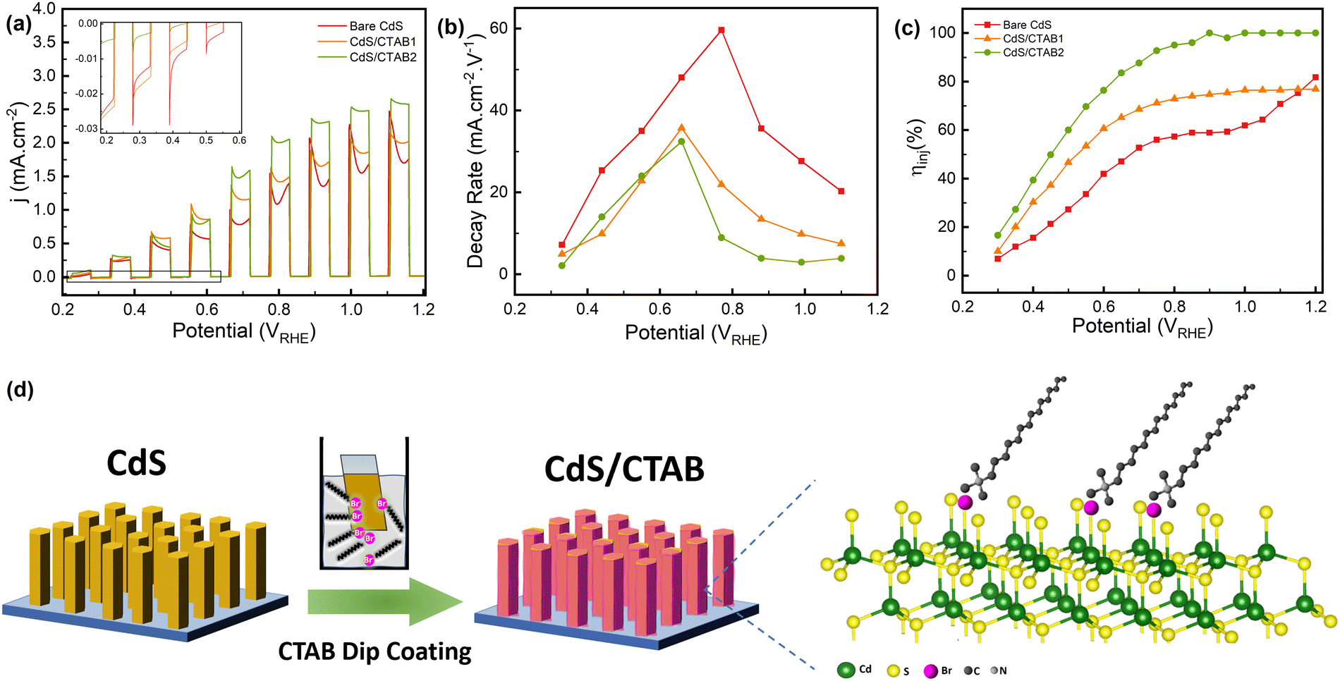 | ||
| Fig. 2 (a) Chopped illumination LSV, (b) decay rates of the photocurrent after the anodic spike, (c) ηinj of are CdS, CdS/CTAB1, and CdS/CTAB2. (d) The schematic representation of the adsorption model of CTAB on CdS after dip coating. | ||
The hole transfer, accumulation, and extraction behavior of the photoanodes can be monitored from the transient behavior of photocurrent density. Starting from 0.2 V, there is an anodic spike every time the photoanode is illuminated, and these spikes are followed by a decay in photocurrent density (Fig. 2a). The anodic spikes are continuously increasing as more holes are being utilized with the anodic potential sweep and the photocurrent reaches 2.47 mA cm−2 at 1.1 V which is rather promising for bare CdS photoanodes in a scavenger-free alkaline electrolyte. Results demonstrate that as the CTAB coverage increases, the photocurrent density at anodic spikes also increases. In the reported TPC experiments, these anodic spikes and the subsequent decay is associated with the formation of photogenerated charge carriers and the accumulation of holes at the photoanode–electrolyte interface, respectively.32 After the positively charged holes are produced by CdS, they start to migrate to the surface with the band-bending effect.33 However, especially in photoanodes with strong light absorption and carrier utilization characteristics like CdS, the rate of photogenerated holes that arrive at the surface is higher than their injection into the electrolyte for OER. In Fig. 2b, the decay kinetics of photocurrent density was investigated by estimating the photocurrent decay rates after each anodic spike. For the bare CdS, the photocurrent decay rate increases up to 0.77 V and then it becomes slower as the potential increases. The potential where the decay rate starts to decrease shows a cathodic shift for the CTAB-decorated photoanodes indicating the enhanced OER kinetics. At potentials below 0.66 V, the decay rate of CdS/CTAB1 and CdS/CTAB2 are close to each other whereas the decay rate of CdS/CTAB2 is the lowest above 0.66 V. In the proposed adsorption mechanism of CTAB which is shown in Fig. 2d, Br− occupies the surface Svs, therefore, the decreased decay rate with CTAB shows that Svs have an important role in the activity loss of CdS.
Generally, photocurrent density is expected to reach a steady state after this decay when the production of charge carriers and the injection of holes to the electrolyte are in equilibrium. However, starting from 0.2 V, another anodic event subsequent to the initial photocurrent decay is observed. This pattern, photocurrent density going through a dip, repeats itself between 0.2 V to 1.2 V which means that there is a change either on the photoanode surface or in the ionic species at the photoanode/electrolyte interface. This type of behavior has been reported for different photoanodes before,34,35 but very little information regarding its potential dependence is available. It is known that CdS is sensitive to chemical and light-induced corrosion during PEC experiments. Especially in electrolytes without a hole scavenger, it can dissolve into the electrolyte as Cd2+ and S2−.36–39 Sulfide species are electrochemically unstable ions, and they can easily undergo electrochemical oxidation under applied anodic bias. Caliari et al.40 reported that the electrochemical oxidation of S2− to SO42− takes place at potentials between 0.475 V and 1.0 V which is consistent with the behavior in Fig. 2a. Since the anodic event after the photocurrent decay is in the same potential window, we attribute this behavior to the oxidation of S2− which is dissolved from the CdS due to photocorrosion.
In addition to this anodic behavior, after photocurrent dip under illumination, there is a cathodic spiking between 0.2 and 0.7 V when the light is off (inset of Fig. 2a). This spike can be explained by the recombination of holes and electrons at the surface when photoexcitation is interrupted. It starts from 0.2 V in bare CdS and shows a gradual decrease until it disappears completely at 0.7 V. There is a correlation between these cathodic spikes and S2− oxidation peaks because of the lower kinetic overpotential required for S2− oxidation. Another factor that could contribute to suppressed cathodic spikes is the enhanced charge separation at higher potentials which facilitates water oxidation. However, the cathodic spikes disappear at the same potential region where the anodic photocurrent gains momentum. It is thus more plausible that S2− oxidation contributes to this trend of cathodic spikes. The intensity of cathodic spikes decreases significantly in CdS/CTAB1 and they almost disappear in CdS/CTAB2. The elimination of the surface charge recombination with the CTAB overlayer corresponds to boosted charge separation and utilization.
In addition to chopped illumination LSV measurements, photoanodes were tested under continuous illumination in the presence and absence of Na2SO3 hole scavenger (Fig. S6a and b, ESI†) to investigate the potential dependent evolution of ηinj. In Fig. 2c, more efficient utilization of photogenerated holes in the presence of CTAB is evident. It is clear that CTAB acts like a hole-extracting layer on the surface, suppressing the accumulation of holes at the photoanode/electrolyte interface, however, this role appears to be valid up to 0.7 V. The possible reason for steady ηinj at higher potentials could be provided by EIS investigations.
EIS was performed to investigate the changes in charge transfer resistance (RCT) with the anodic and cathodic spikes through the anodic sweep. The details of the measurements and fittings of the Nyquist plots are given in Fig. S7 (ESI†). In Fig. 3a, it is shown RCT of bare CdS decreases with CTAB treatment and CdS/CTAB2 has the lowest RCT, which is consistent with the LSV measurements. However, the potential dependent behavior of RCT of the photoanodes shows a surprising trend.
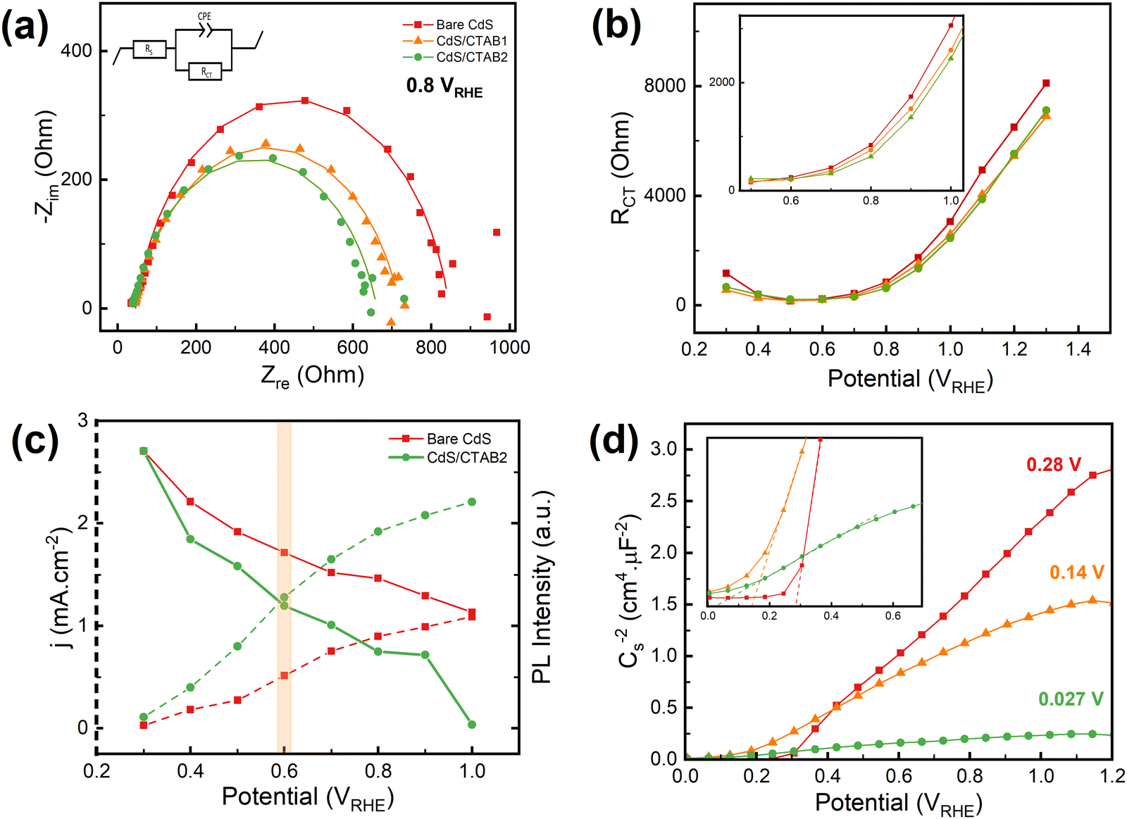 | ||
| Fig. 3 (a) Nyquist plots recorded at 1.0 V and (b) the potential dependent RCT plots of bare CdS, CdS/CTAB1, and CdS/CTAB2. (c) LSV and in situ PL emission plots of bare CdS and CdS/CTAB2. The PL measurements were performed by using the same 3-electrode configuration of PEC experiments in a quartz spectroscopy cuvette. The PL emission intensities were normalized with respect to the emission at 0.3 V by peak area integration. (d) MS plots of bare CdS, CdS/CTAB1, and CdS/CTAB2 (measured in dark). | ||
Fig. 3b demonstrates that RCT starts to decrease from 0.3 V and reaches a plateau at 0.5 V for all photoanodes. This steady resistance continues until 0.7 V and starts to increase gradually with applied potential. Through the anodic scan, the RCT of the bare CdS is higher than that of CdS/CTAB1 and CdS/CTAB2 except for the 0.5–0.7 V region. However, RCT is generally expected to decrease with increasing applied potential due to enhanced charge separation and utilization.41 Even though the photocurrent density of all photoanodes increases through the whole potential range, RCT shows an increase starting from 0.7 V. Note that the change in RCT behavior falls into the same region in LSV measurements where the anodic spikes after the photocurrent dipping under illumination starts. This behavior might have the same origin that S2− ions are highly reactive and they tend to donate their electrons to the photoanode to give an oxidation reaction. The increase in the charge transfer resistance can be associated with the additional resistance resulting from the S2− oxidation products accumulating on the surface. Note that more than one process, such as charge accumulation, OER, and S2− oxidation, takes place simultaneously whenever the light is on in the chopped illumination LSV measurements. We consider the S2− oxidation as an activity-diminishing factor that is happening simultaneously with OER.
PL emission spectroscopy was used to provide a supporting characterization study for the effect of CTAB decoration. It is a characterization technique that is often used to investigate charge carrier recombination characteristics.42 In Fig. 3c the photocurrent density and the in situ PL emission intensity of bare CdS and CdS/CTAB2 are presented as a function of applied potential. Results demonstrate that the PL emission intensity of CdS/CTAB2 is lower than that of bare CdS at all potentials. Both photoanodes show a gradual decrease in emission intensity as photocurrent density increases, which is expected since the electron–hole recombination is less at higher potentials due to enhanced charge separation. Between 0.3 V and 0.6 V, the emission intensity of CdS/CTAB2 decreases 1.5 times faster than that of bare CdS. After 0.6 V, the normalized emission intensity of CdS/CTAB2 decreases by 4.1% up to 1.0 V while bare CdS decreases by 2% within the same potential range. This result is consistent with the chopped illumination LSV data where the effect of CTAB is more dominant at potentials above 0.6 V.
The transient behavior of open circuit potential (OCP) was also investigated to probe the effect of CTAB on photovoltage. The photovoltage change for CdS photoanodes is shown in Fig. S8 (ESI†). The OCP of bare CdS is 0.67 V and it decreases with CTAB overlayer. Generally, it is considered as a negative effect for photoanodes, because lower OCP means less self-driven potential for the OER. However, it has been reported elsewhere that the modification of photocatalyst with hydrophilic surface passivation overlayers might result in interfacial dipole formation which shifts the band-edge position and causes lower OCP.43 After the light is switched on, all photoanodes show a fast OCP decay with photoexcitation of electrons in the valence band and subsequent formation of electron–hole pairs.44 CdS/CTAB2 reaches the lowest potential compared to bare CdS and CdS/CTAB1. Higher photovoltage upon illumination can be attributed to strong light utilization and more photogenerated charge carriers migrating to the space-charge region. However, the OCP values upon illumination are very close to each other. Notice that, although bare CdS has the highest photovoltage change, it shows a slight decrease during illumination while CTAB-decorated photoanodes remain flat. It is an indication of lower surface charge recombination and improved injection of photogenerated holes to the electrolyte.45
In Fig. 3d, Mott Schottky (MS) plots show positive slopes characteristic of n-type semiconductors. Analysis results demonstrate that the flat band potential (Vfb) displays a cathodic shift from 0.28 to 0.027 V with CTAB treatment in agreement with cathodic shifts in the onset potentials of LSV curves. A more negative Vfb upon CTAB adsorption provides a higher quasi-Fermi level of electrons (EF,n). Photovoltage then increases due to a greater separation between the quasi-Fermi level of holes (EF,p) and EF,n. The slope of the MS plot for bare CdS shows a significant decrease with the CTAB treatment. Among all photoanodes, CdS/CTAB2 reveals the smallest MS slope, however, linking this to the highest donor density (Nd)46 must be done with precaution. It is important to note that the effect of surface morphologies and complex reactions that take place at the photoanode/electrolyte interface are neglected in the MS analysis. Other than modifications on bulk structure, such as the addition of a dopant that can act like an electron donor, the potential dependent capacitive behavior at the space charge layer is the contributing factor that can influence the linear behavior of the MS plot. Such non-linearity might have been caused by the change in the surface electronic structure after CTAB decoration where surface sulfur vacancies are being occupied by Br− of CTAB.47
Another set of chopped illumination LSV measurements was performed to investigate the relation of the CTAB adsorption mechanism to the surface Sv content by using the H2O2-treated CdS samples. The experimental details are given in ESI.† In the literature, Svs have been utilized for CdS photocatalysts to create electron trap centers that can favor reduction reactions such as hydrogen evolution, CO2 reduction, and N2 reduction.48–50 Inspired by these studies, the effect of Svs on the photoelectrochemical response of CdS has been investigated. In Fig. S9a and b (ESI†), Cd 3d and S 2p XPS spectra and the change in Cd and S species after H2O2 treatment are given, respectively. The gradual decrease in the S 2p and Cd 3d peaks, and the shift towards higher binding energy is attributed to the formation of Svs.51 The Sv content is calculated based on a method reported for CdS42 and an increase in the amount of surface Sv with H2O2 treatment is shown in Table S1 (ESI†). Br 3d XPS spectra in Fig. S9c (ESI†) show that the amount of Br on CdS_Sv/CTAB is higher than that of CdS/CTAB1. This is in strong agreement with our adsorption hypothesis of Br− on the CdS surface.
After the surface characterization, the PEC activities of the samples were measured. In Fig. S10a (ESI†), chopped illumination LSV results show that H2O2 treatment decreases the PEC activity of CdS photoanodes (CdS_Sv). Svs are the abundant n-type defects of CdS.52 At an optimum level, they can enhance the charge carrier mobility in bulk phase.53 However, surface Svs can act like electron trap centers and cause surface charge recombination which decreases the photocurrent density. This can be the reason for deactivation after H2O2 treatment. After the formation of surface Svs, the photoanodes were kept in 0.03 M CTAB solution for 2 h like CdS/CTAB1 (CdS_Sv/CTAB). According to the chopped illumination LSV results presented in Fig. S10a and b (ESI†), CTAB treatment increases the photocurrent density of CdS_Sv and bare CdS by 98% and 52%, at 1.1 V, respectively. It is consistent with our hypothesis where CTAB is adsorbed on the surface by occupation of surface Sv with Br−. Additional Svs created make more binding sites available for CTAB adsorption, and it can further enhance charge utilization.
For CdS_Sv, the photocurrent decay observed after the anodic spikes upon illumination is less intense than the pristine CdS. In Fig. S10a (ESI†), 0.7 V and 0.8 V are given as highlighted regions. Notice that, in the first region, CdS_Sv does not show the anodic rise after the photocurrent decay. It indicates that H2O2 treatment leads to a cathodic shift in the dip behavior which is associated with the oxidation of dissolved S2−. In this region, the photocurrent decay rates calculated as in Fig. 2b showed that the decay rate of bare CdS is 2 times higher than that of CdS_Sv, which is in strong agreement with the interpretation of TPC behavior. Moreover, the photocurrent density after the dip increases by 9.4% and 40% for CdS_Sv and bare CdS, respectively. Since the CdS_Sv surface has an increased number of Svs, less photo-corrosion induced S2− is released to the electrolyte, thus, less S2− undergoes oxidation reaction on the photoanode surface to cause faster photocurrent decay and increased interfacial RCT. Moreover, MS analysis results shown in Fig. S10c and d (ESI†) reveal that CdS_Sv and CdS_Sv/CTAB photoanodes have higher Nd than bare CdS and CdS/CTAB1, respectively. We demonstrated that as the CTAB overlayer amount increases, The Vfb potential of bare CdS shows a negative shift and Nd increases. It is important to note that the amount of change in these variables might be ambiguous because MS analysis only applies under certain assumptions. However, the results support the XPS spectra in Fig. S9c (ESI†) where the CTAB overlayer amount on CdS_Sv is higher than that of bare CdS after the same dip-coating time.
As mentioned earlier, understanding the activity loss paths and the parameters is very important for both investigation of CdS charge carrier dynamics and understanding the activity improvement after surface CTAB decoration. Therefore, within the light of PEC and structural characterization experiments, the S2− oxidation hypothesis was tested in detail by transient chronoamperometric (CA) measurements to reveal the mechanistic fingerprints of the elementary steps of charge carrier utilization. CA-TPC experiments were conducted to further analyze the photocorrosion and photocurrent density decay behavior by using 250 ms on 250 ms off light pulses with an LED light source at 0.7 V. The CA-TPC results of bare CdS and CdS/CTAB2 are shown in Fig. 4. Notice that the anodic spike, subsequent decay, and the cathodic spike when the light is off are all consistent with the chopped illumination LSV observations. However, what is unexpected is the wiggle-like periodic cathodic events observed during short illumination.
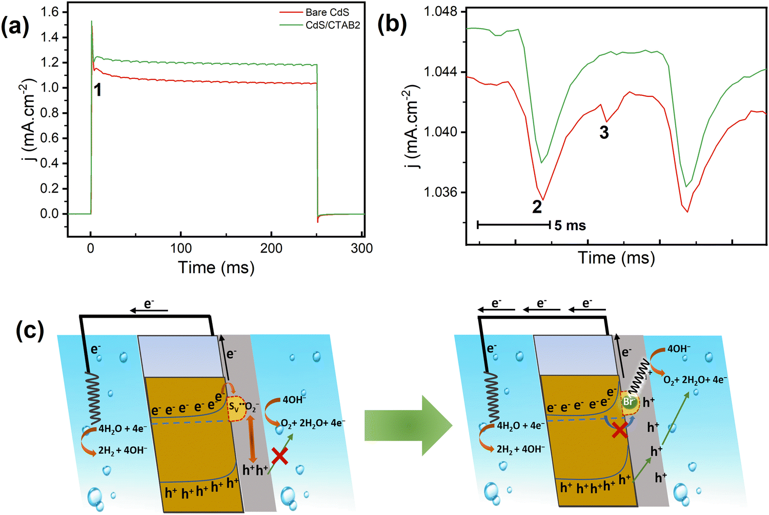 | ||
| Fig. 4 (a) CA at 0.7 V with 250 ms white LED light pulse of bare CdS and CdS/CTAB2, (b) stacked inset of the wiggle behavior under illumination, (c) schematic representation of the effect of CTAB on surface charge trapping passivation. | ||
In Fig. 4b, a stacked inset of one wiggle which takes around 10 ms is shown with 2 cathodic events numbered as 2 and 3. We propose the trapping mechanism below, which can explain the periodicity of 2 cathodic events and the relation between S2− dissolution and the activity loss.
Water oxidation mechanism
| CdS → e− + h+ |
| * + OH− + h+ → *OH |
| *OH + OH− + h+ → *O + H2O |
| *O + OH− + h+ → *OOH |
| *OOH + OH− + h+ → O2(g) + H2O |
Photocorrosion mechanism
| CdS → Cd(aq)2+ + S(aq)2− |
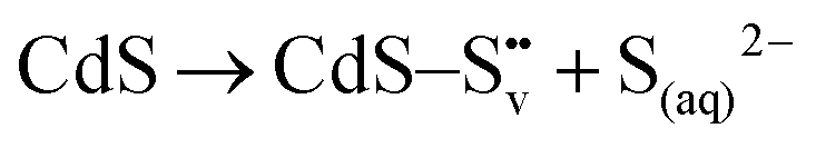
| (1) |
| S(aq)2− + 2h+ → S0 |
| 2S(aq)2− + 3O2(g) + H2O + 4h+ → 4SO4(aq)2− |
Electron trapping mechanism

| (2) |
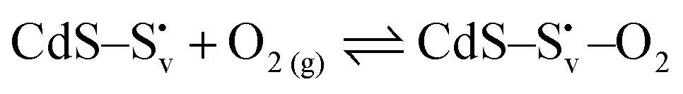
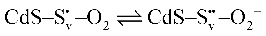
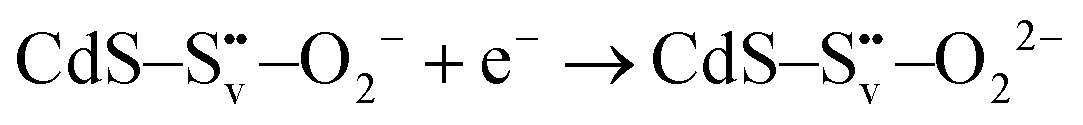
| (3) |
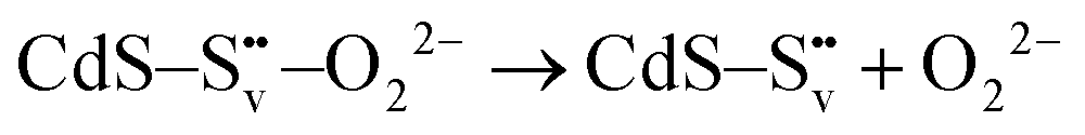
| (4) |
| O22− + 2h+ → O2(g) | (5) |
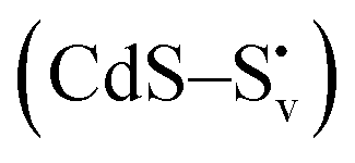 and transform into an adsorbed superoxide (O2−) which is known to be very reactive. Event number 3 then can be attributed to the reduction step in eqn (3), the conversion of adsorbed O2− into a peroxide (O22−). Notice that this event disappears in CdS/CTAB2 because of the occupancy of Svs with Br−. In this way, photogenerated holes could drive OER more effectively rather than getting involved in undesired recombination at the surface due to electron trapping. What makes this process periodic is that, after recovering its double valency (
 ), O22− can desorb from the surface (eqn (4)). O22− could then be involved in further oxidation reactions (eqn (5)).
In the photocorrosion and electron trapping mechanism, 3 important parameters can change the extent of trapping: applied potential, light intensity, and illumination time. The change in potential could manipulate the amount of O2 evolving and the last 2 parameters can be used to tune the amount of Svs. In order to show the effect of these parameters 3 CA experiments were conducted by using bare CdS as the control sample. In Fig. S11a (ESI†), a snapshot of 250 ms on 250 ms off pulse experiment at 3 different potentials is shown. Notice that as the potential increases the intensity of cathodic peaks increases as well. Normally, if there is a trapping event that is caused only by a trap state, it is expected to decrease with applied potential. However, it is vice versa for CdS, which is consistent with our hypothesis where the O2 evolving is a part of the trapping mechanism. Secondly, we performed the same experiment at 2 different light intensities. Since the Sv formation on the surface depends on light-induced dissolution, exposure to intenser light could lead to the formation of a greater number of Svs that are eventually involved in surface charge recombination and cathodic events. The result in Fig. S11b (ESI†) and the PEC activity decrease after H2O2 treatment in Fig. S9a (ESI†) confirm this hypothesis as they both show the negative effect of surface Svs.
Lastly, the effect of light-induced Sv formation is investigated by changing the illumination time at 0.7 V. Similar to light intensity-dependent tests, an increased number of Svs could be extended as the photoanode is illuminated for a longer time. For 50 ms and 150 ms long illumination measurements, there was no cathodic spike when the light is turned off. However, a cathodic spike appears at 500 ms and continues to increase until 1200 ms where it reaches a maximum. This behavior is associated with the recombination of accumulating holes on the surface with electrons. Notice that the photocurrent density at each anodic spike when light is on and photocurrent demonstrating a decaying trend are both decreasing between 50 to 1200 ms due to the surface charge recombination involving trapped electrons. Meanwhile, cathodic spikes when the light is off are increasing, which is associated with surface charge recombination. The result confirms Fig. S11b (ESI†) which shows that when more surface Svs form by photo-dissolution, electron trapping goes to a higher extent. Moreover, the cathodic spikes start to decrease after 1200 ms illumination meanwhile the photocurrent decaying over time starts to increase. For the chopped illumination LSV experiment, we associated the anodic event after photocurrent decay with the S2− oxidation. It is important to note that longer illumination not only creates Svs on the surface but also causes more S2− dissolution which can undergo electrochemical oxidation at 0.7 V. This reversed trend of cathodic spike and the photocurrent density can be attributed to this electrochemical process which was also confirmed by EIS measurements.
Conclusion
In summary, a set of PEC characterization experiments were performed to investigate the fundamental charge transfer and utilization processes of CdS photoanodes, and a facile post-synthesis surface modification method was suggested for more efficient hole utilization. Results showed that Svs, both abundant and formed by photocorrosion, play a critical role in the surface charge carrier dynamics of CdS. Results demonstrate that Svs can act like electron trap centers causing surface charge recombination. We proposed a surface electron trapping mechanism to explain the photocurrent decay behavior in chopped illumination LSV measurements, which was further confirmed by short-light pulse CA measurements. A combination of LSV, TPC, and in situ PL spectroscopy investigations revealed that the CTAB overlayer can passivate the surface electron trapping and electron–hole recombination processes via the occupation of Svs by Br−. To investigate the effect of surface Svs on the extent of electron trapping and the adsorption mechanism of CTAB, both bare and surface Sv-rich CdS photoanodes were analyzed by XPS before and after CTAB treatment to see the change in surface composition. Overall, we provided a detailed set of TPC experiments which showed that the electron trapping on the CdS surface is strongly correlated with the Svs and also the extent of OER. We believe that this work can be an important insight for research on CdS photoanodes by providing a fundamental understanding of key processes taking place at the photoanode/electrolyte interface.Conflicts of interest
The authors declare no conflict of interest.Acknowledgements
The authors thank KUYTAM for the characterization measurements and E. Ö. A. and S. K. would like to thank technicians of Tüpraş R&D Center Laboratories for collaborative research support.References
- A. Gautam, S. Sk and U. Pal, Recent advances in solution assisted synthesis of transition metal chalcogenides for photo-electrocatalytic hydrogen evolution, Phys. Chem. Chem. Phys., 2022, 24, 20638–20673 RSC.
- J. Huang, Y. Jiang, T. An and M. Cao, Increasing the active sites and intrinsic activity of transition metal chalcogenide electrocatalysts for enhanced water splitting, J. Mater. Chem. A, 2020, 8, 25465–25498 RSC.
- K. C. Majhi and M. Yadav, Transition Metal-Based Chalcogenides as Electrocatalysts for Overall Water Splitting, ACS Eng. Au, 2023, 3, 278–284 CrossRef CAS.
- X. Chen, Z. Zhang, L. Chi, A. K. Nair, W. Shangguan and Z. Jiang, Recent Advances in Visible-Light-Driven Photoelectrochemical Water Splitting: Catalyst Nanostructures and Reaction Systems, Nano-Micro Lett., 2016, 8, 1–12 CrossRef CAS PubMed.
- C. Prasad, N. Madkhali, J. S. Won, J. E. Lee, S. Sangaraju and H. Y. Choi, CdS based heterojunction for water splitting: A review, Mater. Sci. Eng. B, 2023, 292, 116413 CrossRef CAS.
- J. Wang, Y. Pan, L. Jiang, M. Liu, F. Liu, M. Jia, J. Li and Y. Lai, Photoelectrochemical Determination of Cu2+ Using a WO3/CdS Heterojunction Photoanode, ACS Appl. Mater. Interfaces, 2019, 11, 37541–37549 CrossRef CAS PubMed.
- Y. Li, Z. Liu, J. Zhang, Z. Guo, Y. Xin and L. Zhao, 1D/0D WO3/CdS heterojunction photoanodes modified with dual co-catalysts for efficient photoelectrochemical water splitting, J. Alloys Compd., 2019, 790, 493–501 CrossRef CAS.
- S. Chen, C. Li and Z. Hou, A novel in situ synthesis of TiO2/CdS heterojunction for improving photoelectrochemical water splitting, Int. J. Hydrogen Energy, 2019, 44, 25473–25485 CrossRef CAS.
- M. Ruan, X. Cai, Y. Lan and H. Xing, Hexagonal CdS photoanode modified with Pt and cobalt phosphate cocatalyst for efficient photoelectrochemical performance, Mater. Lett., 2020, 260, 126947 CrossRef.
- J. Zhang, J. Cui and S. Eslava, Oxygen Evolution Catalysts at Transition Metal Oxide Photoanodes: Their Differing Roles for Solar Water Splitting, Adv. Energy Mater., 2021, 11, 2003111 CrossRef CAS.
- M.-H. Sun, M.-Y. Qi, Z.-R. Tang and Y.-J. Xu, Dual cocatalysts decorated CdS nanoparticles for efficient dehydrocoupling of thiols into disulfides, Appl. Catal., B, 2023, 321, 122019 CrossRef CAS.
- S. Zheng, L. Han, X. Luo, L. Sun, N. Li, Z. Zhang and X. Li, Polydopamine and Nafion bi-layer passivation modified CdS photoanode for photoelectrochemical hydrogen evolution, Int. J. Energy Res., 2022, 46, 4506–4515 CrossRef CAS.
- R. Wang, L. Wang, Y. Zhou and Z. Zou, Al-ZnO/CdS Photoanode Modified with a Triple Functions Conformal TiO2 Film for Enhanced Photoelectrochemical Efficiency and Stability, Appl. Catal., B, 2019, 255, 117738 CrossRef CAS.
- S. A. Vanalakar, M. P. Suryawanshi, S. S. Mali, A. V. Moholkar, J. Y. Kim, P. S. Patil and J. H. Kim, Simplistic surface active agents mediated morphological tweaking of CdS thin films for photoelectrochemical solar cell performance, Curr. Appl. Phys., 2014, 14, 1669–1676 CrossRef.
- M. B. Vishlaghi, A. Kahraman, N. Österbacka, E. Usman, E. Erdem, A. Sennaroğlu, J. Wiktor and S. Kaya, Accelerating water oxidation on BiVO4 photoanodes via surface modification with Co dopants, J. Mater. Chem. A, 2023, 11, 16648–16658 RSC.
- A. Dumbrava, G. Prodan, D. Berger and M. Bica, Properties of PEG-capped CdS nanopowders synthesized under very mild conditions, Powder Technol., 2015, 270, 197–204 CrossRef CAS.
- T. Senasu, T. Chankhanittha, K. Hemavibool and S. Nanan, Visible-light-responsive photocatalyst based on ZnO/CdS nanocomposite for photodegradation of reactive red azo dye and ofloxacin antibiotic, Mater. Sci. Semicond. Process., 2021, 123, 105558 CrossRef CAS.
- N. Ben Brahim, M. Poggi, J.-C. Lambry, N. Bel Haj Mohamed, R. Ben Chaâbane and M. Negrerie, Density of Grafted Chains in Thioglycerol-Capped CdS Quantum Dots Determines Their Interaction with Aluminum(III) in Water, Inorg. Chem., 2018, 57, 4979–4988 CrossRef CAS PubMed.
- S. Muniyappan, T. Solaiyammal, B. G. T. Keerthana, P. Vivek and P. Murugakoothan, Influence of annealing temperature on structural, morphological and optical properties of CTAB assisted cadmium sulphide (CdS) quantum dots: promising candidate for quantum dot sensitized solar cell (QDSSC) applications, J. Mater. Sci.: Mater. Electron., 2017, 28, 11317–11324 CrossRef CAS.
- Q. Li, R. P. Antony, L. H. Wong and D. H. L. Ng, Promotional effects of cetyltrimethylammonium bromide surface modification on a hematite photoanode for photoelectrochemical water splitting, RSC Adv., 2015, 5, 100142–100146 RSC.
- J. Sun, Y. Wang, S. Guo, B. Wan, L. Dong, Y. Gu, C. Song, C. Pan, Q. Zhang, L. Gu, F. Pan and J. Zhang, Lateral 2D WSe2 p–n Homojunction Formed by Efficient Charge-Carrier-Type Modulation for High-Performance Optoelectronics, Adv. Mater., 2020, 32, 1906499 CrossRef CAS PubMed.
- A. Lippitz, J. F. Friedrich and W. E. S. Unger, Plasma bromination of HOPG surfaces: A NEXAFS and synchrotron XPS study, Surf. Sci., 2013, 611, L1–L7 CrossRef CAS.
- G. Hota, S. B. Idage and K. C. Khilar, Characterization of nano-sized CdS–Ag2S core-shell nanoparticles using XPS technique, Colloids Surf., A, 2007, 293, 5–12 CrossRef CAS.
- P. Innocenzi, P. Falcaro, D. Grosso and F. Babonneau, Order−Disorder Transitions and Evolution of Silica Structure in Self-Assembled Mesostructured Silica Films Studied through FTIR Spectroscopy, J. Phys. Chem. B, 2003, 107, 4711–4717 CrossRef CAS.
- M. I. De Barros, J. Bouchet, I. Raoult, T. Le Mogne, J. M. Martin, M. Kasrai and Y. Yamada, Friction reduction by metal sulfides in boundary lubrication studied by XPS and XANES analyses, Wear, 2003, 254, 863–870 CrossRef CAS.
- D. Meissner, R. Memming, B. Kastening and D. Bahnemann, Fundamental problems of water splitting at cadmium sulfide, Chem. Phys. Lett., 1986, 127, 419–423 CrossRef CAS.
- P. Thangadurai, S. Balaji and P. T. Manoharan, Growth and mechanism of CdS nanorods by microstructure analysis, Mater. Chem. Phys., 2009, 114, 420–424 CrossRef CAS.
- Y. Na, B. Hu, Q.-L. Yang, J. Liu, L. Zhou, R.-Q. Fan and Y.-L. Yang, CdS quantum dot sensitized p-type NiO as photocathode with integrated cobaloxime in photoelectrochemical cell for water splitting, Chin. Chem. Lett., 2015, 26, 141–144 CrossRef CAS.
- M. E. Orazem, I. Frateur, B. Tribollet, V. Vivier, S. Marcelin, N. Pébère, A. L. Bunge, E. A. White, D. P. Riemer and M. Musiani, Dielectric Properties of Materials Showing Constant-Phase-Element (CPE) Impedance Response, J. Electrochem. Soc., 2013, 160, C215 CrossRef CAS.
- S. Jostar, S. Devadason and J. Suthagar, Effect of CdS layers on opto-electrical properties of chemically prepared ZnS/CdS/TiO2 photoanodes, Mater. Sci. Semicond. Process., 2015, 34, 65–73 CrossRef.
- Z. Chen, T. G. Deutsch, H. N. Dinh, K. Domen, K. Emery, A. J. Forman, N. Gaillard, R. Garland, C. Heske, T. F. Jaramillo, A. Kleiman-Shwarsctein, E. Miller, K. Takanabe and J. Turner, in Photoelectrochemical Water Splitting: Standards, Experimental Methods, and Protocols, ed. Z. Chen, H. N. Dinh and E. Miller, Springer, New York, NY, 2013, pp. 87–97 Search PubMed.
- E. Usman, M. Barzgar Vishlaghi, A. Kahraman, N. Solati and S. Kaya, Modifying the Electron-Trapping Process at the BiVO4 Surface States via the TiO2 Overlayer for Enhanced Water Oxidation, ACS Appl. Mater. Interfaces, 2021, 13, 60602–60611 CrossRef CAS PubMed.
- S. Corby, E. Pastor, Y. Dong, X. Zheng, L. Francàs, M. Sachs, S. Selim, A. Kafizas, A. A. Bakulin and J. R. Durrant, Charge Separation, Band-Bending, and Recombination in WO3 Photoanodes, J. Phys. Chem. Lett., 2019, 10, 5395–5401 CrossRef CAS PubMed.
- C. Guo, K. Tian, L. Wang, F. Liang, F. Wang, D. Chen, J. Ning, Y. Zhong and Y. Hu, Approach of Fermi level and electron-trap level in cadmium sulfide nanorods via molybdenum doping with enhanced carrier separation for boosted photocatalytic hydrogen production, J. Colloid Interface Sci., 2021, 583, 661–671 CrossRef CAS PubMed.
- K. K. Kasem, Long-Term Activity of Thermoplastic Gel Electrolyte in a Photo-Electrochemical Assembly Involving Poly Bithiophene (PBTh) as Photoactive Working Electrode, J. Mater. Sci. Chem. Eng., 2021, 9, 1–11 CAS.
- L. Wei, Z. Guo and X. Jia, Probing Photocorrosion Mechanism of CdS Films and Enhancing Photoelectrocatalytic Activity via Cocatalyst, Catal. Lett., 2021, 151, 56–66 CrossRef CAS.
- D. J. Fermín, E. A. Ponomarev and L. M. Peter, A kinetic study of CdS photocorrosion by intensity modulated photocurrent and photoelectrochemical impedance spectroscopy, J. Electroanal. Chem., 1999, 473, 192–203 CrossRef.
- D. Meissner, R. Memming and B. Kastening, Photoelectrochemistry of cadmium sulfide. 1. Reanalysis of photocorrosion and flat-band potential, J. Phys. Chem., 1988, 92, 3476–3483 CrossRef CAS.
- T. Inoue, T. Watanabe, A. Fujishima, K. Honda and K. Kohayakawa, Suppression of Surface Dissolution of CdS Photoanode by Reducing Agents, J. Electrochem. Soc., 1977, 124, 719–722 CrossRef CAS.
- P. C. Caliari, M. J. Pacheco, L. F. Ciríaco and A. M. C. Lopes, Anodic Oxidation of Sulfide to Sulfate: Effect of the Current Density on the Process Kinetics, J. Braz. Chem. Soc., 2017, 28, 557–566 CAS.
- R. Attias, B. Dlugatch, M. S. Chae, Y. Goffer and D. Aurbach, Changes in the interfacial charge-transfer resistance of Mg metal electrodes, measured by dynamic electrochemical impedance spectroscopy, Electrochem. Commun., 2021, 124, 106952 CrossRef CAS.
- D. W. DeQuilettes, K. Frohna, D. Emin, T. Kirchartz, V. Bulovic, D. S. Ginger and S. D. Stranks, Charge-Carrier Recombination in Halide Perovskites: Focus Review, Chem. Rev., 2019, 119, 11007–11019 CrossRef CAS PubMed.
- Y.-G. Lee, S. Park, W. Cho, T. Son, P. Sudhagar, J. H. Jung, S. Wooh, K. Char and Y. S. Kang, Effective Passivation of Nanostructured TiO2 Interfaces with PEG-Based Oligomeric Coadsorbents To Improve the Performance of Dye-Sensitized Solar Cells, J. Phys. Chem. C, 2012, 116, 6770–6777 CrossRef CAS.
- T. M. Burke, S. Sweetnam, K. Vandewal and M. D. McGehee, Beyond Langevin Recombination: How Equilibrium Between Free Carriers and Charge Transfer States Determines the Open-Circuit Voltage of Organic Solar Cells, Adv. Energy Mater., 2015, 5, 1500123 CrossRef.
- J. Su, C. Liu, D. Liu, M. Li and J. Zhou, Enhanced Photoelectrochemical Performance of the BiVO4/Zn:BiVO4 Homojunction for Water Oxidation, ChemCatChem, 2016, 8, 3279–3286 CrossRef CAS.
- W. Chakhari, J. Ben Naceur, S. Ben Taieb, I. Ben Assaker and R. Chtourou, Fe-doped TiO2 nanorods with enhanced electrochemical properties as efficient photoanode materials, J. Alloys Compd., 2017, 708, 862–870 CrossRef CAS.
- Y. Fu, C.-L. Dong, Z. Zhou, W.-Y. Lee, J. Chen, P. Guo, L. Zhao and S. Shen, Solution growth of Ta-doped hematite nanorods for efficient photoelectrochemical water splitting: a tradeoff between electronic structure and nanostructure evolution, Phys. Chem. Chem. Phys., 2016, 18, 3846–3853 RSC.
- Y. Wang, X. Xu, W. Lu, Y. Huo and L. Bian, A sulfur vacancy rich CdS based composite photocatalyst with g-C3N4 as a matrix derived from a Cd–S cluster assembled supramolecular network for H2 production and VOC removal, Dalton Trans., 2018, 47, 4219–4227 RSC.
- T. Tian, X. Jin, N. Guo, H. Li, Y. Han and Y. Yuan, CdS/ethylenediamine nanowires 3D photocatalyst with rich sulfur vacancies for efficient syngas production from CO2 photoreduction, Appl. Catal., B, 2022, 308, 121227 CrossRef CAS.
- X. Zheng, H. Han, J. Liu, Y. Yang, L. Pan, S. Zhang, S. Meng and S. Chen, Sulfur Vacancy-Mediated Electron–Hole Separation at MoS2/CdS Heterojunctions for Boosting Photocatalytic N2 Reduction, ACS Appl. Energy Mater., 2022, 5, 4475–4485 CrossRef CAS.
- L. Cheng, Y. Li, A. Chen, Y. Zhu and C. Li, Impacts on carbon dioxide electroreduction of cadmium sulfides via continuous surface sulfur vacancy engineering, Chem. Commun., 2020, 56, 563–566 RSC.
- K. Sharma, A. Kumar, T. Ahamad, Q. V. Le, P. Raizada, A. Singh, L. H. Nguyen, S. Thakur, V.-H. Nguyen and P. Singh, Sulphur vacancy defects engineered metal sulfides for amended photo(electro)catalytic water splitting: A review, J. Mater. Sci. Technol., 2023, 152, 50–64 CrossRef.
- J. He, L. Hu, C. Shao, S. Jiang, C. Sun and S. Song, Photocatalytic H2O Overall Splitting into H2 Bubbles by Single Atomic Sulfur Vacancy CdS with Spin Polarization Electric Field, ACS Nano, 2021, 15, 18006–18013 CrossRef CAS PubMed.
- Q. Zhu, Z. Xu, Q. Yi, M. Nasir, M. Xing, B. Qiu and J. Zhang, Prolonged electron lifetime in sulfur vacancy-rich ZnCdS nanocages by interstitial phosphorus doping for photocatalytic water reduction, Mater. Chem. Front., 2020, 4, 3234–3239 RSC.
Footnote |
| † Electronic supplementary information (ESI) available. See DOI: https://doi.org/10.1039/d3ma00847a |
| This journal is © The Royal Society of Chemistry 2024 |