
 Open Access Article
 This Open Access Article is licensed under a Creative Commons Attribution-Non Commercial 3.0 Unported Licence
Fourth-generation solar cells: a review
Fatima
Rehman
 a,
Iqrar Hussain
Syed
a,
Saira
Khanam
a,
Sumbel
Ijaz
a,
Haris
Mehmood
a,
Muhammad
Zubair
*b,
Yehia
Massoud
*b and
Muhammad Qasim
Mehmood
*a
a,
Iqrar Hussain
Syed
a,
Saira
Khanam
a,
Sumbel
Ijaz
a,
Haris
Mehmood
a,
Muhammad
Zubair
*b,
Yehia
Massoud
*b and
Muhammad Qasim
Mehmood
*a
aMicroNano Lab, Department of Electrical Engineering, Information Technology University (ITU) of the Punjab, Ferozepur Road, 54600 Lahore, Pakistan. E-mail: qasim.mehmood@itu.edu.pk
bInnovative Technologies Laboratories (ITL), King Abdullah University of Science and Technology (KAUST), Thuwal 23955, Saudi Arabia. E-mail: muhammad.zubair.3@kaust.edu.pk; yehia.massoud@kaust.edu.sa
First published on 26th June 2023
Abstract
Solar cells have provided a solution to the prevailing energy crisis and environmental contamination in the ongoing energy-driven era because of their potential to utilize solar energy. The initial efforts devoted to this during the past century involved the use of p–n junctions of III–V semiconductors (gallium arsenide, gallium nitride) which resulted in only low-efficiency solar cells. Conventional energy sources, through carbon dioxide emissions, contaminate the environment and exacerbate the greenhouse effect. By contrast, solar technology, as a sustainable form of energy, has assisted in mitigating these challenges, and the quest for attaining efficient and sophisticated designs has led to the discovery of a variety of solar cell structures. However, their large-scale commercialization has been constrained due to many factors, which include the vast installation area required, expensive cost, limited durability and associated losses that lead to a smaller operating efficiency, all of which have opened up various research routes to overcome these shortcomings. The diligent attempts of researchers have converged into generation-by-generation improvements in this domain. In this paper, we have discussed the design and working principles, fabrication, simulation and mathematical modelling of the most advanced state-of-the-art fourth-generation solar cells, which consist mainly of 2D material-based solar cells, quantum dot-based solar cells (QDSCs), perovskite solar cells (PSCs), organic solar cells (OSCs) and dye-sensitized solar cells (DSSCs). The comprehensive literature review presented in this paper may help the solar cell community to investigate and become acquainted with the design opportunities and variations that exist in the technology under study.
1. Introduction
One of the major challenges faced by nations around the globe is the energy crisis. The shortage of energy resources can lead to a poorer economy and increased inflation, which eventually destabilises a state. Researchers around the world are trying, therefore, to discover novel resources that may contribute to reducing the shortage of energy while simultaneously keeping the environment clean. Unlike conventional energy resources, which are exponentially depleting the Earth's natural resources and producing harmful byproducts, scientists have been looking for environmentally friendly alternatives. Solar cells (SCs) have been found to be a promising technology that can overcome the energy-shortage challenge whilst also meeting the need for environmental sustainability. Sunlight acts as a source of energy and is a gift of nature that is abundantly available around the world. The process of photo-excitation in solar cells produces photo-generated electrons which then generate electricity. However, an unequivocal limitation exists that is related to associated losses, such as transmission losses, thermalization, and recombination losses,1 which lowers the overall efficiency of the cell.2 Researchers worldwide have been working on solar cell technology to optimize the cell performance; this is achieved by ruling out the causes of low output, which is accomplished through engineering of both the materials and the design structures.The history of solar cells dates back nearly five decades. The advancements made in solar cell technology have led to the formation of many generations of SCs. First-generation SCs comprise mono- and polycrystalline silicon solar cells.3 They were first discovered in 1954 when Bell Laboratories announced the invention of silicon solar cells with an efficiency of 8%,4 which were reported to be the most efficient solar cells of that time. Although, silicon solar cells achieved the highest efficiencies, they were very expensive because of their manufacturing cost, thus hindering their large-scale deployment. This inspired the search for alternative materials that were both cost effective and possessed the excellent properties of silicon. This led to the introduction of second-generation solar cells, which in general are also called thin-film solar cells. These solar cells are comprised mainly of amorphous silicon (a-Si), copper indium gallium selenide (CIGS) and cadmium telluride (CdTe),5 due to their wide bandwidth that enables the absorption of solar radiation.6 The bandgap of a material affects the range of solar wavelengths it can absorb, which in turn causes efficient charge transport and charge collection within a certain energy range (also known as the bandwidth), and hence it is considered crucial for maximizing the photocurrent and, consequently, the PCE of a solar cell.7,8 Although materials belonging to second-generation SCs showed cost-effectiveness, they had significant drawbacks of toxicity, instability and low efficiency.9 Consequently, thin-film solar cells also failed to be utilized for large-scale applications. With the passage of time, advances were made in PV technology, which led to another evolution in this field and resulted in the discovery of third-generation solar cells. Third-generation solar cells offered a number of design variations, including dye-sensitized solar cells (DSSCs), quantum dot sensitized solar cells (QDSCs), organic solar cells (OSCs) and perovskite solar cells (PSCs).10 Their applicability in a particular scenario is evaluated based on their associated merits and demerits; for instance, a DSSC has the ability to work in dim light, but the electrolyte in the DSSC is organic in nature, which is volatile and can evaporate if not sealed properly. Similarly, PSCs are cheaper to manufacture11 as they can be produced using easy fabrication techniques and by using inexpensive materials.12 They also offer the highest power conversion efficiency, although they are prone to environmental degradation as the perovskites are sensitive to heat and humidity, which hinders their large-scale production.13 Likewise, OSCs are environmentally friendly, lightweight and semitransparent,14 in addition to being one of the cheapest sources of electricity;15 they do, however, lack stability and have a relatively short lifetime16 as presented by Gevorgyan et al.17 Quantum dot-based solar cells are durable, have high efficiencies and offer tunability. However, some types of QDSSC, such as cadmium selenide (CdSe) quantum dots, are highly toxic18 and pose a threat to the ecosystem. The quest for designing increasingly efficient and stable solar cells encouraged the development of fourth-generation solar cells, which is the latest technology in this research area. Fourth-generation solar cells combine all the benefits exhibited by solar cells of previous generations because they are cheaper, they have flexible structures, and they also offer the high stability of nano-materials.19 They are also called hybrid solar cells because of their ability to incorporate inorganic materials with organic materials.20 They are commonly made up of metal oxides and metal nanoparticles, carbon nanotubes, graphene and its derivatives.21 A detailed analysis of the efficiencies of the different generation solar cells along with their historical timeline is given in Fig. 1.
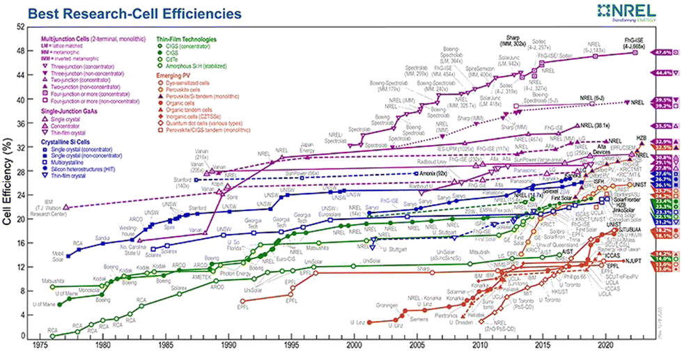 | ||
| Fig. 1 Best research cell efficiency chart.22 | ||
In this review, our objective is to give an overview of contemporary developments, as well as the needs and installation of fourth-generation solar cells, while highlighting their advancements in comparison with previous-generation solar cells. The main focus is to discuss and elaborate on the design and working principles, their fabrication, the simulation methods and mathematical modelling. The continuous attempts to improve their performance rely on different design metrics, which include selection of the appropriate material and structure as well as the working principle in accordance with a particular configuration. Since all solar cells follow the same working principle for the conversion of solar energy into electrical energy, thus we will begin by describing the process of photogeneration that is equally valid for all types of solar cell.
1.1 Photogeneration
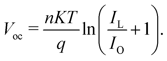
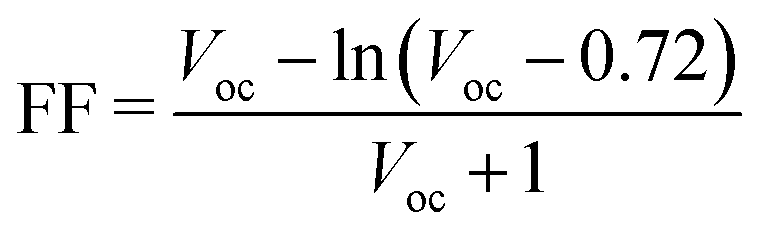
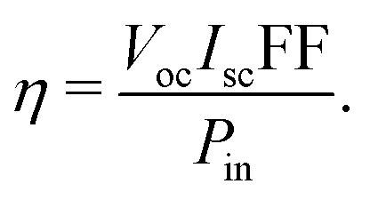
Photogeneration is the process of generating excitons (bound electron–hole pairs) as a result of photon absorption. The net generation of charge carriers depends on both exciton creation and dissociation since excitonic absorption does not necessarily result in mobile charges. Solar cells are characterized by this effect, i.e., the formation of electron–hole pairs when light is incident on them. The phenomenon is manifested with the help of a structure that consists of a junction between n-type silicon and a p-type absorber which is placed between two electrodes, as shown in Fig. 2. The process is completed effectively in the following steps: the first step is the absorption of light (photons), i.e., the generation of charge carriers. As shown in Fig. 2(a), a single photon of light is incident on the solar cell, and, upon its absorption, an exciton pair is produced. For the second step, Fig. 2(b) shows the disassociation of the exciton into charge carriers and the collection of these carriers at the electrodes. Several excitons are generated at once with a full spectrum of light, and these are simultaneously separated into independent charge carriers. Once these carriers are generated in a solar cell, they move around due to various processes such as diffusion, random motion and drift. In order to separate the photo-generated charged carriers, semi-permeable membranes are a must for both sides of the absorber, which ensure that the electron can only pass from one membrane and the holes flow out from another membrane. The charges are generated in the absorber layer, the p–n junction (at the top) allows only electrons to pass through, and the membrane at the bottom of the cell allows only holes to pass through; therefore, the solar cell needs to be designed in such a way that the mobile charge carriers hit these barriers so they can be separated, as shown in Fig. 2(c). The difference in the concentration of charge carriers at both ends of the PV device causes a potential difference between the electrodes, and this potential, which can be measured using a voltmeter, is called the open circuit voltage (Voc). If an external circuit is applied between the electrodes, the flow of electrons takes place from the n-type to the p-type material, thus producing electricity. In other words, the chemical energy of the electron–hole pair is changed into electrical energy Fig. 2(d and e). After the electrons have passed via the circuit they recombine with holes at the interface between the metal and absorber (Fig. 2(f)). Another major phenomenon that occurs during the formation of excitons is “recombination”. The exciton pair survives independently only for a particular lifetime, after which recombination may occur due to the weakening of the coulombic forces between them. This means that the electron will return to its initial state if recombination happens and the energy that was absorbed initially will be lost, hindering the conversion of light energy to electrical energy. In general, the performance of a SC is measured according to its operating parameters, which include the open circuit voltage Voc (V), the short circuit current Jsc (mA cm−2), the fill factor (FF; %) and the power conversion efficiency (PCE; %) (Fig. 2(g–i)). The success of PV technology lies in engineering the system in such a way that the performance parameters are optimized using various salient features, such as the carrier mobility, control of the recombination and other losses. In the upcoming sections, we will be reviewing two-dimensional material-based SCs, quantum dot SCs, perovskite SCs, organic SCs and dye-sensitized SCs.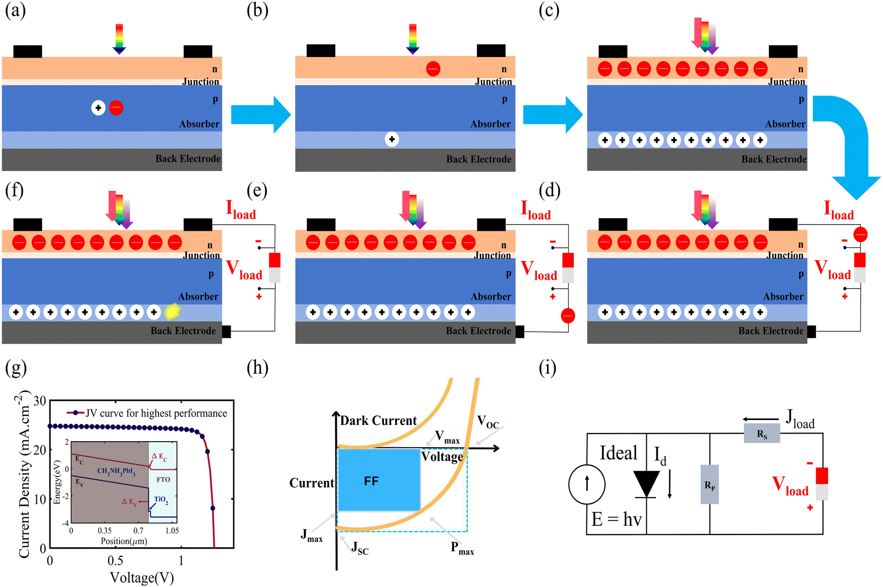 | ||
| Fig. 2 (a) Absorption of a single photon of light, (b) generated and separated charge carriers, (c) continuous generation and separation of charge carriers, (d) load is connected, (e) movement of a charge carrier from high potential to low potential, (f) combining electron and holes, (g) J–V curve, where the inset shows the energy band diagram, (h) J–V curve, where the inset shows the maximum efficiency, and (i) equivalent electrical model. | ||
2. Two-dimensional (2D) material-based solar cells
2D materials such as molybdenum disulphide (MoS2), graphene, tungsten disulphide (WS2) and tungsten diselenide (WSe2) have gained immense interest in fourth-generation photovoltaic technology due to their exceptional optical properties, thin sizes and lightweight nature.23 MoS2, WS2 and WSe2 belong to the family of transition metal dichalcogenides (TMDCs), whereas graphene is an allotrope of carbon. These 2D materials are well-known for their flexibility, mechanical strength, transparency, tunable band gap, high carrier mobility and good conduction of heat and electricity, quantum Hall effect and magnetic anisotropy.24–29 These properties are attributed to their quantum confinement.30 Owing to these exceptional properties, 2D materials, in particular graphene and its nanostructures, have so far shown potential applications in many fields, which include biomedical,31,32 electronics,33 photonics,34 membrane technology,35 energy sector36,37 and sensor designs38 to name but a few. Different types of 2D materials have been employed in the design of a variety of solar cells because they have the ability to be used as a transparent electrode, an electron transport material, a hole transport material, an active layer, a buffer layer, and an ultrathin and transparent diffusion barrier.23,39 Graphene is used in photovoltaic devices chiefly due to its tightly packed, two-dimensional honeycomb structure (Fig. 3(a)),40 and plays a special role in protecting PV devices from environmental degradation.41 Similarly, the trigonal prismatic structure of 2D materials is shown in Fig. 3(b). In comparison with the most widely used solar absorbers GaAs and Si, 2D TMDC materials have successfully achieved an order of magnitude improvement in sunlight absorption and, notably, are capable of absorbing between 5 and 10% of incident sunlight for a material thickness of less than 1 nm.42 Single layer MoS2 can be used in conjunction with p-Si to fabricate heterojunction solar cells.43 MoS2 also has the tendency to form a heterostructure with WSe2 for use as counter electrodes in DSSCs.44 Similarly, graphene has also been employed in its various forms; for instance, its fluorescent quantum dots,45 nanotubes,46 fullerenes47 and nanoribbons48 have been used extensively in solar cell technology. In addition, different chemical functionalization protocols can be followed to improve the electrical and optical properties of 2D materials, and doping can be carried out to enhance these properties.49 These 2D materials have seemingly endless potential for improving the existing technologies of SCs. The different fabrication techniques also affect the morphology of the material.50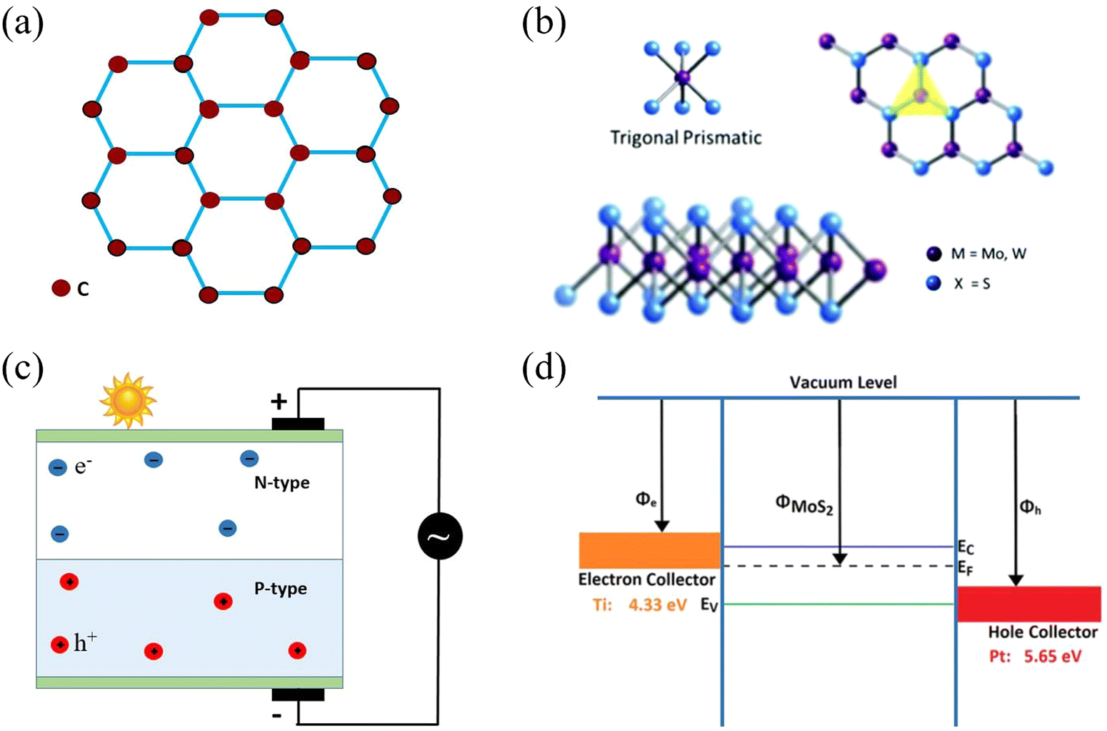 | ||
| Fig. 3 (a) Honeycomb hexagonal structure of graphene. (b) Structure of 2D materials in terms of the metal coordination (top), and stacking sequence (bottom) of 2H MoS2 and WS2. (c) Working principle of a photovoltaic cell (reprinted under Open Access51). (d) Schematic diagram in terms of the band structure of a Schottky junction Ti–MoS2–Pt solar cell (reprinted from ref. 52 under a CC-BY license). | ||
2.1 Design and working principle of 2D material-based solar cells
Solar cells are constructed using semiconductor layers of n-type, i.e., the emitter layer, and p-type, i.e., the base layer, thus developing a p–n junction as shown in Fig. 3(c). The reflections are reduced by using an anti-reflection coating layer. Solar cells, also identified as photovoltaic cells, have been designed for the direct conversion of light (photo) into electricity (voltaic), i.e., “energy from light”. Light is electromagnetic radiation that is comprised of photons that are basically quanta of energy. The photon energy E is given in eqn (1):| E = hv | (1) |
When light falls on a surface, the loosely bound electrons absorb it and are promoted to their excited states, leaving behind vacancies called holes, where the hole is a positively charged entity. There is a coulombic force of attraction between the negatively charged electrons and the positively charged holes, forming pairs which are known as excitons.54
The intrinsic energy possessed by the electrons in the valence band (VB) is Ei, and after excitation the energy is raised to Ef in the conduction band (CB) only if the incident photon has an energy equal to or greater than that of the band gap55 (i.e., Ei − Ef ≥ hv), where the band gap is a forbidden region between the CB and the VB. The migration of electrons results in current flow.56
2.2 Fabrication techniques for 2D material-based solar cells
Multi-layers of 2D materials can be prepared using the Scotch tape method,57 the CVD (chemical vapour deposition) technique58,59 and other electro-chemical methods.60,61 Cai et al. have presented detailed information on the synthesis of 2D materials using top-down exfoliation techniques.62 In the subsequent sub-section the fabrication methods for graphene are described, and similar techniques can be used to synthesise other 2D materials. | ||
| Fig. 4 Mechanical exfoliation or Scotch tape method. | ||
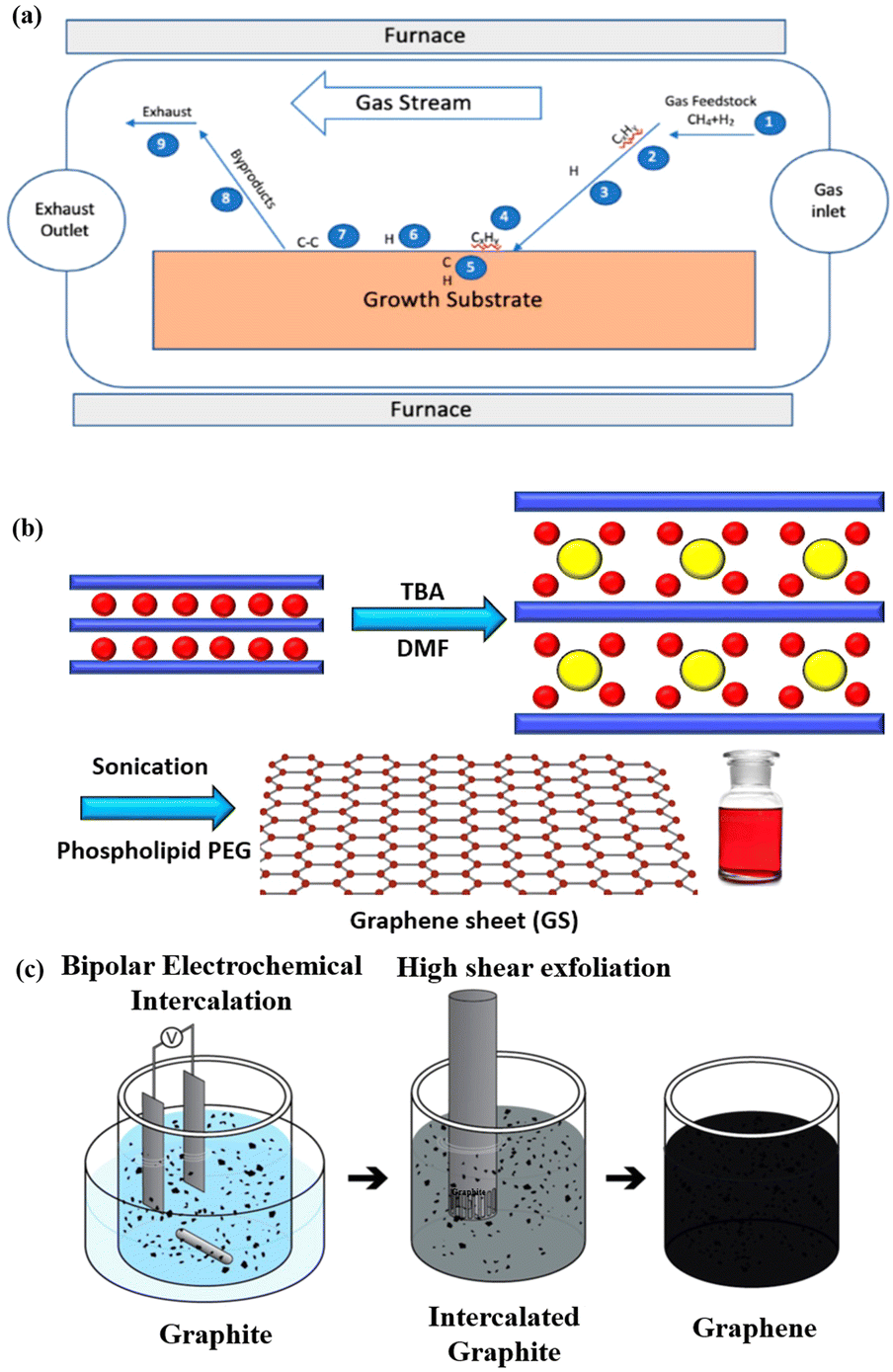 | ||
| Fig. 5 (a) Stepwise method for the chemical vapour deposition of graphene (reproduced with permission from Saeed et al. published by MDPI, Molecules, 2020).68 (b) Chemical method to synthesise aqueous graphene sheets using tetrabutylammonium hydroxide (TBA) in water and N,N-dimethylformamide (DMF). (c) Electrochemical method to fabricate aqueous graphene using bipolar electrochemical intercalation and high shear exfoliation (reprinted with special permission from ACS, further permissions related to the material excerpted should be directed to the ACS71). | ||
![[thin space (1/6-em)]](https://www.rsc.org/images/entities/char_2009.gif) 000 s−1. The mixture was then centrifuged to remove any remaining big particles of graphite, and the residual liquid was extracted. By filtering a specific quantity of the suspension using poly(tetrafluoroethylene) (PTFE) membrane filters, the production of graphene in every suspension was calculated. The graphene sheets made using this technique were structurally intact.
000 s−1. The mixture was then centrifuged to remove any remaining big particles of graphite, and the residual liquid was extracted. By filtering a specific quantity of the suspension using poly(tetrafluoroethylene) (PTFE) membrane filters, the production of graphene in every suspension was calculated. The graphene sheets made using this technique were structurally intact.
2.3 Simulation and mathematical modelling of 2D material-based solar cells
The simulation and mathematical modelling of different solar cells are indeed interrelated. Both approaches are commonly used in the field of solar cell research and have been developed to understand the behavior, performance, and efficiency of solar cells. These methods refer to the use of computer-based models and algorithms to mimic and analyze the physical and electrical characteristics of solar cells, in which solving complex mathematical equations and incorporating various parameters, such as material properties, device geometry, and environmental conditions, are carried out. Mathematical modelling involves the formulation of mathematical equations and analytical frameworks that describe the behavior and performance of solar cells. These models are based on fundamental physical principles and are used to predict and analyze multiple aspects of the operation of a solar cell, such as the energy conversion efficiency, current–voltage characteristics, and the spectral response. Such modelling provides a theoretical understanding of a solar cell to serve as a basis for further analysis and optimization. In ref. 77 and 78 the authors verified that the simulated and experimental values for the solar cell characteristics are approximately the same. The authors simulated and fabricated SHJ-p-type aSi:H and measured the open circuit voltage, short circuit current, fill factor and efficiency. This provides a relationship between the theory and experimental ideas to analyze the optical and electrical characteristics of a solar cell, confirming that the basic design proposed for the simulations is correct. Several software platforms have so far been used to conduct the simulations for graphene-based solar cells, and include Ansys,79 COMSOL,80 AFORS-HET,81 CST-MWS82 and SILVACO(TCAD)83 to describe the physical mechanisms taking place within the device. The WF (Φ (eV)), the thicknesses of the layers, the density of interface states, absorption loss, band gap, Voc (V), Jsc (mA cm−2), PCE, and FF are the design elements of solar cell that need to be evaluated. As a myriad of topologies can be realized for graphene-based cells, therefore it becomes essential to carry out an initial investigation of the influence of the aforementioned parameters on the device performance via simulations to save both cost and time. The AFORS-HET software is frequently used for modelling hetero-junctions with intrinsic thin-layer (HIT) solar cells as well as hetero-junction (HJ) solar cells. For instance, Yu et al.81 used this tool to analyse the efficiency of the graphene/GaAs-based cell before conducting actual experiments to ascertain the effect of the addition of a hole-transporting or electron-blocking layer. Methodical examination of the impact of many variables, such as the carrier density, absorption loss, and graphene WF, has been performed on the proposed device. This study demonstrates the enormous potential for using the graphene/GaAs HJ in extremely efficient solar cells. It has been demonstrated that graphene's WF, which is roughly 5 eV, endorses the improvement of efficiency. The WF of graphene is optimised chiefly by overcoming the absorption loss. A schematic diagram of the silver/graphene/n-GaAs/silver Schottky HJ solar cell is shown in Fig. 6(a), for which the AFORS-HET software was used to calculate the energy-band diagrams for the cell under study (as presented in Fig. 6(b)) by changing the graphene WFs to observe the variation in the performance of the HJ solar cell. By applying Shockley–Read–Hall (SRH) recombination statistics, the AFORS-HET software solves the continuity equations and 1-D Poisson equation, such that one may analyse the behaviour of HJ SCs.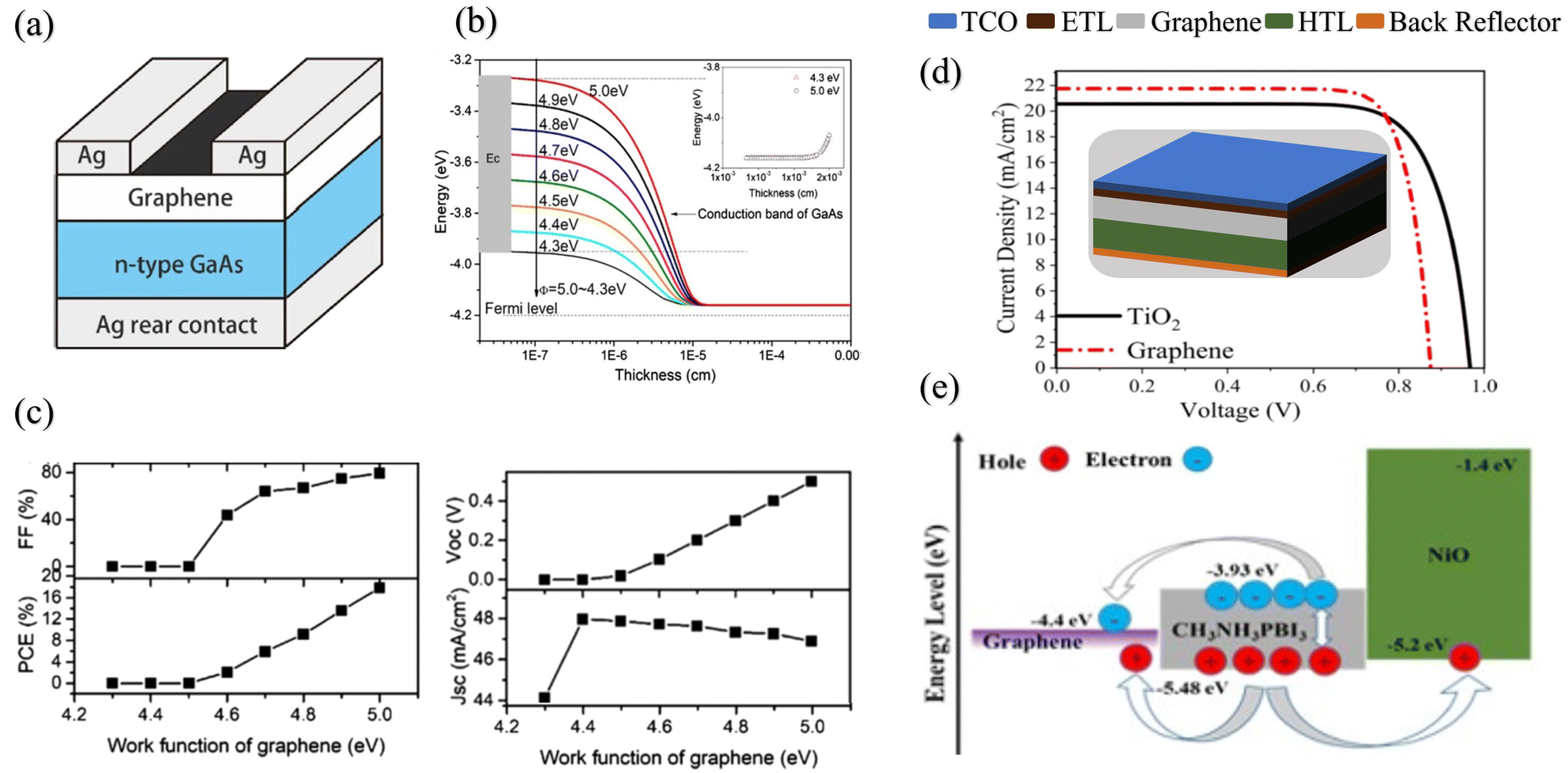 | ||
| Fig. 6 (a) Simulated graphene/GaAs HJ solar cell schematic. (b) Graphene/GaAs energy band diagram for multiple graphene WF values, where the inset shows the location of the back contact on the conduction band diagram when the graphene WF is changed from 4.3 to 5.0 eV. (Source: Yu et al.;81 copyright 2019 licensed under Copyright Clearance Center, Inc.) (c) Output performance parameters of the graphene/GaAs HJ SCs with different graphene WFs. (d) Layer thicknesses and 3D PSC schematic (inset), and current density vs. voltage for ETLs of TiO2 and graphene. (e) Energy level diagram and carrier transportation system in the PSC with the graphene ETL. (Source: Dadashbeik et al.;84 copyright 2020 licensed under Copyright Clearance Center, Inc.) | ||
The conduction band on the GaAs side exhibits greater bending and a bigger depletion zone with the increase in the WF of graphene from 4.3 to 5.0 eV. In addition, the energy band diagrams of the graphene/GaAs HJ cell at the location of the back contact when the graphene WF is changed from 4.3 from 5.0 eV are included in the inset of Fig. 6(b). It is observed that the energy band diagram at the back contact is hardly affected by graphene's WF. This occurs principally because of the lower breadth of the built-in electric field when compared to the thickness of the GaAs layer. In Fig. 6(c), the output performance parameters of the graphene/GaAs HJ SCs are presented for the different WFs of graphene. The Voc (V), FF and PCE values increase considerably, where the PCE increases to 17.84% for WF = 5.0 eV. However, the Jsc increases in the beginning from 44.12 to 47.92 mA cm−2 upon increasing the WF from 4.3 to 4.4 eV, and then subsequently decreases to 46.8 mA cm−2 for WF = 5.0 eV. As another example, authors of ref. 84 presented a 3D graphene solar cell using finite-element method (FEM)-based simulations. The layers in the cell structure are shown in Fig. 6(d), where FTO layer acts as the transparent conducting oxide (TCO), the n-type material TiO2 is the electron transport layer (ETL), an intrinsic layer (I-layer) of the perovskite CH3NH3PbI3 is the active layer, a p-type material is used as the hole transport layer (HTL), and an Au layer acts as the back reflector. The authors investigated the respective effects of the ETL composed of graphene and a TiO2/graphene nano-composite on the absorption, carrier production and recombination, charge transport, Jsc, Voc, and PCE. It is observed from Fig. 6(d) that the presence of the graphene ETL enhances the absorption of the absorber layer due to its favourable optical as well as electrical characteristics, since the carrier mobility in graphene is very significant compared with TiO2, which is expressed as an increase in Jsc from 19.07 to 21.73 mA cm−2, the fill factor (FF) increased from 76.3% to 82.8% and the PCE increased from 14.42% to 16.03%. At the same time, due to recombination at the interface between the active layer and the ETL, the Voc falls from 0.99 to 0.89 V. The band energy level diagram with carrier transport mechanism for the presented cell with graphene acting as the ETL is shown in Fig. 6(e).
Mathematical modelling and simulation are two different but not completely dependent approaches used in the study of photovoltaics. Mathematical modelling involves using mathematical equations to represent the behaviour of a photovoltaic system; it involves developing models that describe the physics of the system, such as the movement of electrons and holes in the solar cells, or models that describe the electrical behaviour of the system, such as the voltage and current produced by the cells. Simulations are based on mathematical models, but may also include other factors such as the effects of temperature and shading. In general, mathematical modelling is intended for developing a fundamental concept related to the behaviour of a photovoltaic system; thus, both approaches are important tools for researchers and engineers, and are often used in combination to develop and optimize solar energy systems. In ref. 85, the authors report the theoretical model for a PV device based on the Pt/graphene/AlGaAs/n-GaAs/Al architecture. The mathematical-model-oriented simulation is carried out using the SILVACO TCAD software. The modelling of graphene is carries our using the 4H-SiC material, whose properties are reformed to contribute to the metallic values provided by Nair et al.86 Three physical models, i.e., Shockley–Read–Hall (SHR) recombination, Auger recombination and Optical recombination (OPTR), are embodied for the design formation of the PV device. The thermionic emission model is employed to represent the J–V characteristics of the heterojunction solar cells. The performance parameter for developing the solar cell mathematically can be expressed as follows in eqn (2):
 | (2) |
 | (3) |
| VBi = (ϕBn − ϕn) | (4) |
| ϕBn = ϕG − χ (n-type-semiconductor) | (5) |
| ϕBp = Eg − ϕg + χ (p-type-semiconductor) | (6) |
 | (7) |
 | (8) |
 | (9) |
The aforementioned mathematical formulas and simulation techniques are equally valid for other 2D materials such as MoS2, WS2 and WSe2.
3. Quantum dot-based solar cells
Quantum dots (QDs) are nanoscale semiconductor crystals that have proved to be fascinating materials in various areas of science, for example, in bio-imaging, light-emitting diode innovation, lasers, and solar cells.88 In general, these materials are formed using II–VI or III–V elements from the periodic table and are characterized to be particles with actual sizes below the Bohr radius of the exciton.88 QDs were first discovered in the 1980s by the Russian physicist Alexei Ekimov.89 Since then, they have attracted extensive research interest.90 They have unique electrical as well as fluorescent properties, which include narrow emission spectra, tunable photoluminescence (PL), high photo-chemical stability, and continuous absorption spectra,90 to highlight but a few. Their unique set of characteristics has enabled them to be used in many applications, which include light emitting diodes, photovoltaics, photoconductors, photodetectors, biosensors, etc. Compared with molecular dyes, quantum dots are better in terms of their tunable photoresponse and higher molar extinction coefficients, enabling a noteworthy increase in the PCE from 5% to 13%.91 Since their discovery more than twenty years ago, their utilization has expanded rapidly as a result of their abundant availability and excellent optical properties. In addition, show other considerable advantages, such as small dimensions (2–12 nm in diameter), size-tunable photo-luminescence,92 high fluorescence quantum yields, high solidness against photo-bleaching, and fluorescence discontinuity (flickering).93 The most frequently used QDs or nanocrystals are cadmium selenide (CdSe), lead selenide (PbSe), cadmium sulphide (CdS), lead sulphide (PbS), cadmium telluride (CdTe), etc.94,95 Control over the size of quantum dots provides leverage for tuning the band gap, which is a distinct advantage over other quantum materials. In addition, due to the shift of energy levels of the CB and VB bands to either more negative or positive values, the quantum confinement effect alters the electronic properties.963.1 Design and working principle of quantum dot-based solar cells
In principle, the aim for designing a quantum dot solar cell (QDSC) is again the conversion of solar energy into an electric current, where QDs behave mainly as light absorbers. The separation transport efficiency as well as the recombination rate of the photogenerated carriers have a significant impact on the QDSC performance. A prototypical QDSC is made of a photoanode comprising a QD-sensitized mesoporous large-bandgap semiconductor (such as TiO2 QDs), an electrolyte, and a counter electrode.97–101 When illuminated with light, photon absorption takes place in the QDs, and the electrons in the VB of the QDs are excited to the CB. Due to the favourable energy gap between the CBs of the QDs and TiO2, the transfer of excited electrons from the CB of the QDs to the CB of TiO2 takes place, from where they are transported to a transparent conducting oxide glass substrate and then to the external circuit. A redox couple electrolyte is used to regenerate oxidized QDs, while attracting electrons from the external circuit at the electrolyte/counter electrode interface is used to regenerate the oxidized electrolyte.99Weller's group published the first research on quantum dot sensitized solar cells (QDSSCs).102 These devices were an alternative to DSSCs on account of the sensitizer used to harvest the sunlight. For DSSCs, the sensitizer is an organic dye molecule/a metal–organic complex, whereas for QDSSCs it is an inorganic semiconductor material. A QDSSC scheme and its operating principle are depicted in Fig. 7(a). The basic structure of a quantum dot SC is shown in Fig. 7(b). QDSCs, in general, have five layers: a quantum dot layer arranged between the HTL and ETL, which are placed between the top metal back electrode layer (Au, Ag, Al) and the bottom photoanode layer (normally ITO or glass). The separation/transport efficiency as well as the recombination rate of the photo-generated carriers have a significant impact on the QDSC performance. A photo-anode, which is also known as a QD-sensitized mesoporous large-band-gap semiconductor, an electrolyte, and a counter electrode make up a typical QDSC.97,98,101 A major requirement for the design of QDSCs is that the semiconductor QDs in a mesoscopic oxide film are assembled and arranged in the correct order and they are deposited on optically transparent electrodes (OTEs), e.g., mesoscopic TiO2 and ZnO films, with a thickness of the order of <10 nm. These electrodes are adjusted with QDs such that the conversion of incident photons to electricity takes place103 as shown in Fig. 7(c). The semiconductor (TiO2) is the best material for the photo-electrode, which reflects all visible light while absorbing ultraviolet light. TiO2 separates the excited electrons from the holes to prevent the recombination of excited electron–holes.102,104
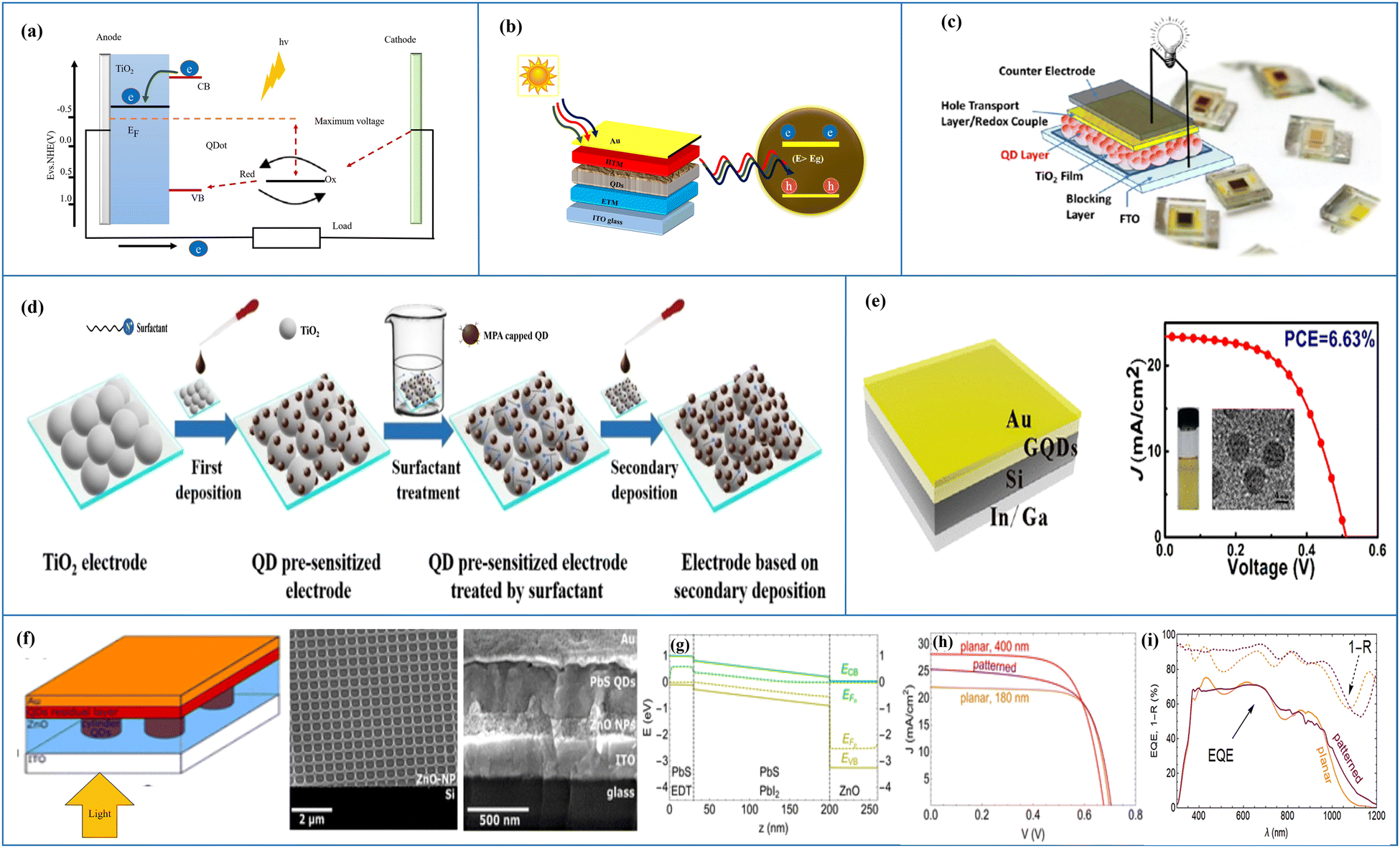 | ||
| Fig. 7 (a) Structure of a QDSSC and its working principle. (b) Schematic diagram of a QDSC. (c) Design of a QDSC made from different layers, where the HTL is a redox electrolyte in the case of liquid junction solar cells and a solid state layer in the case of heterojunction solar cells. The active QD layer is has an area of 0.25 cm2 and is placed between the OTE and the redox electrolyte (reprinted with permission from ref. 103, copyright 2013 American Chemical Society). (d) Secondary deposition method for the fabrication of QD-sensitized photoanodes using surface ligand assisted assembly (reprinted with permission from ref. 105, copyright 2019 American Chemical Society). (e) Left: c-Si/GQD-based heterojunction solar cell. Right: parametric plot (sin(x), cos(x)). (Source: Gao et al.;45 licensed under the terms of the Creative Commons CC). (f) Left: patterned p–i–n heterojunction structure of a PbS quantum dot SC, where the light incidence is from the bottom. The front contact is ITO while the back contact is of Au. Bulk PbS quantum dots behave as a p/i-type layer, while ZnO is the n-type layer, collectively forming a 3D interface. Middle: SEM perspective (45°) view of the SCIL-patterned ZnO nanoparticle layer on a silicon substrate. Right: SEM cross-section image of the patterned cell structure. (g) Band diagram of a PbS quantum dot solar cell (180 nm active layer) under Jsc conditions (V = 0). The conduction band, electron quasi Fermi level (EFn), hole quasi Fermi level (EFp) and valence band are shown from top to the bottom. Gray vertical dashed lines distinguish the different regions in the p–i–n junction. Light is incident from the right. (h) Simulated J–V characteristics for the planar cells with absorber thicknesses of 180 nm (orange) and 400 nm (red), and for a patterned absorber layer (purple). (i) Reflection losses and external quantum efficiency (EQE) of a fabricated planar (orange) and patterned (purple) PbS quantum dot SC, with respect to the wavelength. Solid lines shows the EQE trends, and dashed lines show the upper limits for the EQE (Source: Tabernig et al.;106 licensed under the terms of the Creative Commons CC). | ||
3.2 Fabrication techniques for quantum dot-based solar cells
Several sophisticated methods for the synthesis or fabrication of quantum dot solar cells have been explored so far, such as colloidal synthesis, self-assembly, electrical gating, chemical pyrolysis, traditional aqueous synthesis, the MOCVD growth technique,107 molecular beam epitaxy (MBE),108etc.Multiple spin-coating or dip-coating cycles are typically used in the process of depositing the QD layer. The QD film thickness is determined by the QD concentration and the number of spin or dip cycles. Both approaches yield solar cells that are of comparable performance and highly tunable in terms of the layer thicknesses and ligand exchange. Both deposition methods have their own benefits and deficits. Dip coating needs a sufficient overall volume to completely submerge the substrate. Therefore, the QD solution concentration used during dip coating (e.g., 10–20 mg mL−1) is typically lower than that used for spin coating (30 mg mL−1). Because of the very thin QD films deposited during each cycle, dip coating is used for finer control and is capable of depositing more solar cells from a single QD synthesis. However, this method of deposition normally requires more time because each cycle deposits a limited number of QDs. The deposition of thicker layers per cycle will require a QD higher solution concentration, resulting in film fabrication that is faster, and vice versa for thinner layers.109
Wang et al. used surface engineering to improve the QD loading in QDSCs. When QD pre-sensitized TiO2 films are treated using ammonium cationic surfactants, a supplemental amount of ZCISe (Zn–Cu–In–Se), ZCIS (Zn–Cu–In–S) or CdSe QDs onto ZCISe pre-sensitized electrodes was introduced after secondary deposition, as shown in Fig. 7(d). For the enhanced harvesting of sunlight, QDSCs with a higher QD loading exhibit a significant increase in the Jsc and PCE. So far, a certified PCE of 10.26% for Cu2S/brass counter electrode-based QDSCs has been achieved under simulated AM1.5G test conditions with the secondary deposition of ZCISe QDs.105 As an illustration of the synthesis of QD cells, Gao et al. fabricated graphene quantum dots (GQDs) using Pan's hydrothermal method. They designed a c-Si/GQD-based heterojunction solar cell, which is shown on the left of Fig. 7(e). This unique structure helps to separate the photo-generated electron–hole pairs at the junction. The GQDs have blocked electrons while avoiding charge carrier recombination at the anode. These factors led to the enhanced photovoltaic efficiency of the solar cell. In Fig. 7(e), right, a parametric plot shows that c-Si/GQD-based solar cell reveals relatively good stability; it also retained a high efficiency after storage for six months. An optimum PCE of 6.63% was achieved.45
3.3 Simulation and mathematical modelling of quantum dot-based solar cells
Simulation methods play a crucial role in the development of fourth-generation solar cells. Fourth-generation solar cells refer to a new generation of photovoltaic devices that aim to overcome the limitations of conventional solar cells and offer a higher efficiency, lower cost, and improved functionality. Several factors are included in simulation methods, such as the physics of the device, optimization of the performance, cost reduction via design iteration, and analysis of the material and parameter sensitivity. In ref. 110 and 111, the authors carried out the analysis of various parameters before fabrication of the solar cell. As mentioned before, many software packages have been developed for the design and simulation of solar cells. The underlying physics of quantum dot solar cells can be better understood through simulation and mathematical modelling, which can be used to improve the design for increased efficiency. Such simulations have enabled an in-depth understanding of the various types and locations of recombination to be gained in different device configurations. In addition, these simulation methods are capable of providing information on the dopant and trap state densities of the nanocrystal layers, such that the appropriate selection and optimization of blocking contacts has been carried out to enhance the device performance further.112 These novel high photovoltaic energy conversion efficiency quantum dot sensitized solar cells (QDSSCs) are based on II–VI semiconductor materials such as CdS. CdS is an n-type semiconductor that has a direct band gap energy of 2.42 eV.113 Mehrabian et al. used the SILVACO TCAD software114 to model and simulate the ITO/TiO2/CdS/P3HT/PCBM/Ag structure for a photovoltaic device.115 Another example of simulation of a QDSC is presented in ref. 106, where the design contains a depleted HJ layer (an n-type window layer), bulk PbS QDs ligands PbI2 ligands (an i-type absorber layer), bulk PbS QDs with ethanedithiol (EDT) ligands (a p-type layer) and Au (contact with the back). A matrix of QDs packed tightly together acted as the “bulk QD layer”. Fig. 7(f) shows how an assembly of nano cylinders of PbS quantum dots forms a layer on a residual PbS quantum dot layer and is covered by ZnO. Both the front and back contacts in addition to the p-type layer make planar layers, so the nanopattern is restricted to the i–n junction of the solar cell. An i-type QD layer and a thin p-type QD layer make up the residual QD layer, which serves as an electronic barrier between the back Au contact and the n-type ZnO layer. The dimensions of the pillars were chosen to exhibit strong local optical resonances as well as guided (plasmonic) modes. The pillars are arranged in a square lattice and are placed at a fixed distance apart in the design. There are significantly shorter carrier paths available for those carriers produced at the back of the cell because of their nano geometry and structure that was created via the nanopatterning holes into the ZnO-NP layer (light-blue) on the ITO surface, then filling them with QDs (red). In order to pattern, they employed substrate conformal soft-imprint lithography (SCIL116), which imprints designs onto a liquid sol–gel using a nanostructured PDMS stamp that is a replica of a nanostructured Si master wafer. Until now, optically functional silica-like layers had been patterned using SCIL, and an optically and electronically functional layer was formed by these authors using ZnO-NPs and high-resolution SCIL stamps. This kind of patterned ZnO layer can be seen in the SEM image (Fig. 7(f), middle). It has holes of 400 nm diameter and is arranged in the form of a square lattice with a pitch size of 513 nm. The PDMS stamp's feature depth eliminates the roughly 100 nm height difference between the pattern's walls and the residual ZnO layer. When compared with other conventional patterning techniques that include reactive wet etching and/or ion etching, it is important to note that this nanopattern transfer into the ZnO-NP layer from the stamp is a straightforward method and is highly unlikely to result in undesirable degradation of the ZnO layer's optical or electronic properties. In addition, the ZnO-NP solution used for making the ETL layer is compatible with the current state-of-the-art QD solar cells.117 As a result, there was no need to compromise the quality of the ETL and the SCIL compatibility of its precursor solution. The spinning duration was the only parameter adjusted for ZnO patterning, to ensure that the layer remains in a liquid state such that it can be patterned. Butanol, a solvent with a high boiling point, can be used to dilute the solution. A planar PbS QD-EDT layer of 30 nm and a 100-nm-thick layer of Au were deposited. The i-type material has a planar surface morphology because the nanopattern is restricted to the interface the between QDs and ZnO. As a result, the Au layer and p-type QDs can be conformally deposited in the same manner as a planar cell. After the successful implementation of QD pillars embedded in ZnO, Tabernig et al. analyzed the specific dimensions needed to maximize the performance. For this they studied the optical properties of the bulk PbS QD layers to achieve the highest absorption per unit volume in the patterned absorber via finite difference time domain (FDTD) simulations using Lumerical CHARGE, a drift-diffusion equation solver. The nanostructured geometry of the cell was electronically analysed under an AM1.5G solar spectrum with design parameters including the recombination and doping density, and specific properties of the bulk QD such as its hopping, i.e., the charge transfer process and voltage decrease due to the defects forming an effective CB. The optical simulations performed in ref. 106 revealed a 19.5% increase in the cylindrical QD absorber layer's absorption per unit volume. Electronic simulations have demonstrated that patterning leads to a current gain of 3.2 mA cm−2 and a minor voltage gain, resulting in an efficiency gain of 0.4%. This has been realized for QD nanopillars in a square array with a pitch size of 500 nm on a residual QD layer of 70 nm, surrounded by ZnO. In addition, simulations demonstrate that the patterned structure has a significant impact on the fill factor due to significant variation in the strength of the electric field across the patterned absorber. Due to a significantly enhanced infrared response (as predicted by simulations), Tabernig et al. demonstrated a 0.74 mA cm−2 current gain for a patterned cell in comparison with a planar cell in experimental results, as shown in Fig. 7(f and g). Fig. 7(g) depicts an electronic band diagram for a planar cell that has an absorber thickness of 180 nm and an applied voltage of 0 V. Along the z-direction, the graphs can be divided into three different regions that correspond to the p–i–n-type layers. Depleted heterojunction solar cells typically exhibit band bending, which occurs across the entire i-type layer and is indicative of electric fields.118 The dipole moments of the ligands affect the energy landscape of the bulk QDs, which is why the p-type QD layer has a lower energy offset than the i-type QD layer. Fig. 7(h) shows simulated current–voltage (I–V) curves of planar and patterned cells of 180 and 400 nm thickness under AM1.5G illumination to examine the electronic behaviour of the patterned QD solar cells. The presented device exhibited enhanced light trapping, as proved via EQE measurements as depicted in Fig. 7(i), which was further confirmed with an increase in Jsc (mA cm−2). The lower carrier collection of the patterned device shows less optimal carrier extraction, as affirmed by lower FF values. However, Voc remained unchanged, pointing to the fact that the enhanced surface area does not result in any additional recombination.1064. Perovskite solar cells
The German scientist Gustav Rose discovered the perovskite mineral in 1839,119 although significant exploration on these was carried out by the Russian mineralogist Lev Perovski, hence them being named perovskites.120 Perovskite is a chemical compound of the calcium titanium oxide mineral, which is made up of calcium titanate (CaTiO3)121 and is abundantly available in nature.122,123 Thereafter any compounds having similar crystal structures (orthorhombic shape) were categorised as perovskites.124 Perovskites have a crystal structure with a formula of A(n−1)BnX(3n+1) (where X = halogen, oxygen, nitrogen or carbon). The bigger ‘A’ cation shares a cuboctahedral site with twelve X anions, and the smaller ‘B’ cation shares an octahedral location with six ‘X’ anions.125 Its cubic unit cell is shown in Fig. 8(a). Perovskites exhibit an exceptional ability to absorb light because they transport the electric charge when light falls on them, resulting in an increase in electron mobility.126 Due to their long-range ambipolar charge transport,12 high dielectric constant, high absorption coefficient,127 low exciton-binding energy,128 ferroelectric characteristics,129,130 and other unique physical properties, perovskite materials have sparked a lot of interest for their use in photovoltaic and optoelectronic devices. Since the efficiency of solar cells based on perovskite materials has risen from an initial 3.8% to more than 25%, research interest in these materials has grown dramatically.131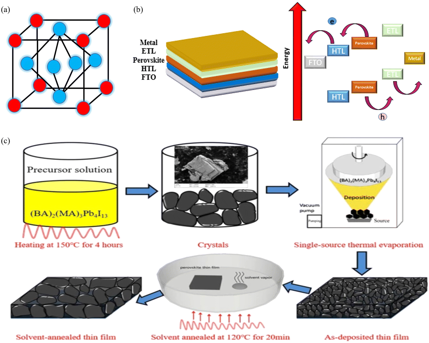 | ||
| Fig. 8 (a) Unit cell of a perovskite. (b) Working principle of the PSC. (c) Schematic diagram of the fabrication procedure, which includes crystal preparation, single-source thermal evaporation, and solvent annealing (source: Zheng et al.;132Sci. Rep., Springer Nature, 2019). | ||
4.1 Design and working principle of perovskite solar cells
The basic layout of a perovskite solar cell (PSC) is shown in Fig. 8(b). It generally has five layers: a perovskite layer is placed between the HTL and the ETL, which are placed between the top metal back electrode layer (Au, Ag, Al) and the bottom photoanode layer (normally ITO or glass). In short, the perovskite active layer is placed at the centre of the solar cell133 which acts as a light absorber. The transparency, thickness and morphology of these layers can be changed to optimise the PCE of the PSC. When light interacts with the perovskite layer, it triggers the emission of photo generated electrons leading to the formation of excitons. Because of the small exciton binding energy of perovskite materials, the excitons separate into electron and holes, which are free charge carriers. These charge carriers then move to the hole- and electron-transport layers and flow towards the anode and cathode of the cell. For PSCs, different architectures exist, such as mesoporous, planar p–i–n, planar n–i–p, and perovskite tandem structures.1344.2 Fabrication techniques for perovskite solar cells
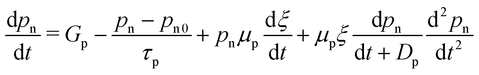
Akin to the development of fabrication techniques for other types of solar cell, there exist several elegant methods for fabricating PSCs. Different coating techniques, such as slot die coating, blade coating, spray coating and other methods, including methylamine gas treatment, scaffold-assisted printing, inkjet printing, screen printing,135 solvent-free pressure assisted coating, vacuum deposition, and hybrid CVD, are used to fabricate large-area perovskite films.136 The spin coating technique137 is also used to synthesize perovskite crystals, although the films produced are not uniform. Casaluci et al. synthesized PSCs using vacuum vapour-assisted solution processing as a simple and inexpensive method without using a glove box. Neither an inert atmosphere nor a high vacuum was used to prepare the devices.138 Li et al. synthesized single-crystal hybrid perovskites using a solution-based lithography-assisted epitaxial growth method.139 The perovskite films made by Zhang et al., using the solvent dripping technique in atmospheric air, were inappropriate for creating highly efficient solar cells in comparison with the mirror-like and brilliant black films created in a dry air glovebox. Since humidity is not favourable for halide perovskites, it is usually avoided during manufacturing. The advances in perovskite fabrication under an ambient environment are hindered by the absence of fundamental knowledge about the chemical reactions between water and the precursors.140 For instance, Zhang et al. successfully demonstrated the suppression of the defects in the formation of organic–inorganic halide PSCs by introducing bilateral interface modification via doping the perovskites with CH3NH3PbI3 nanocrystals at room temperature, resulting in a CsPbBr3-based planar PSC exhibiting a 20% PCE.141 PSCs with the structure ITO/PEDOT:PSS/(BA)2(MA)3Pb4I13/PC61BM/Ag were fabricated via spin coating a solution of PEDOT:PSS (CLEVIOS PVP AI4083) onto glass substrate of ITO. To achieve a 50 nm film, the spin coating parameters were adjusted to 4500 rpm for 40 seconds. The resulting PEDOT:PSS film was heated at 160 °C for 20 minutes; afterwards, it was shifted to a single source evaporation deposition system. The BA2MA3Pb4I13 absorber layer was then deposited using single-source thermal evaporation and solvent annealing was carried out in a glove box filled with nitrogen for 20 minutes at 120 °C. The PC61BM solution (20 mg mL in chlorobenzene) was spin-coated onto the (BA)2(MA)3Pb4I13 thin film at 3000 rpm for 30 s. Finally, a 90 nm Ag cathode was prepared via thermal evaporation under a vacuum of 3.0 × 10⁻⁴ Pa as shown in Fig. 8(c).1324.3 Simulation and mathematical modelling of perovskite solar cells
As has already been said, a variety of solar cell design tools are now accessible for in-depth examination prior to fabrication. In ref. 142, a PSC was modelled and analyzed for its output characteristics under AM1.5G light using SCAPS (the solar cell capacitance simulator). The PV characteristics of the SC were simulated with an emphasis on the absorber layer's depth, recipient percentage, and defect density. In addition, the effects of various metal contact WFs were examined. The optimum parameters for each characteristic were noted for the practical implementation of PSCs, in the interest of contrasting the findings with an experimentally prepared device. SCAPS solves three fundamental equations for a device, including the Poisson eqn (10), which is understood to be the continuity equation of the charge carriers, i.e., electrons (eqn (11)) and the holes (eqn (12)), to obtain the performance details such as the voltage–current density (J–V) characteristics, the quantum efficiency (QE), and the energy bands. These curves are used to calculate the solar cell device's performance parameters of Jsc, Voc, FF (%) and PCE (%).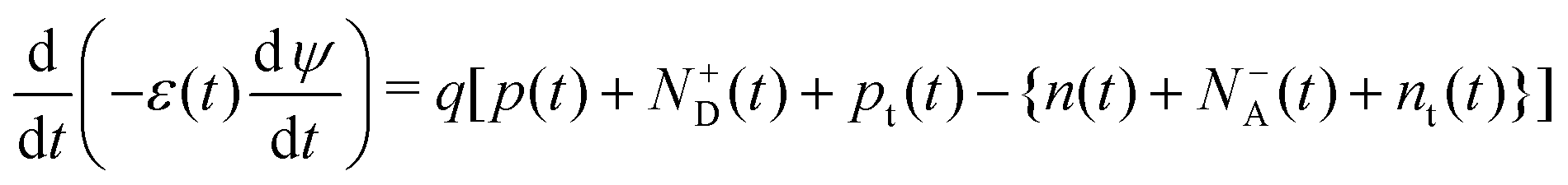 | (10) |
 | (11) |
 | (12) |
Fig. 9(a) depicts the PSC device structure, and when the device is illuminated, excitons develop in the absorber layer. The charge carriers travel towards the ETL and HTL due to the junction field, and afterwards they migrate towards the cathode and anode and are collected at the respective electrodes to produce current. The energy band diagram of the discussed cell is shown in Fig. 9(b). The performance characteristics of the device are plotted in terms of the absorber height in Fig. 9(c). The Jsc shows an increasing trend up to 400 nm, which subsequently saturates to a value of 24.59 mA cm−2. The Voc also increases up to 500 nm and then undergoes a slow decrease as the thickness is increased further. A monotonic decrease is observed in the FF value with the thickness of the absorber layer. A maximum of PCE = 20.96% is obtained at 500 nm; therefore, the optimum absorber thickness is found to be 500 nm. In ref. 146, using SCAPS-1D, the authors modelled a carbon-based PSC that does not have a hole transport layer. The objective of this study was to look for a suitable alternative ETL material in comparison with TiO2 because, when it is used as an ETL, the cell becomes unstable under high temperature and exposure to UV light. Therefore, ZnO, CdZnS, WS2, ZnOS, WO3 and ZnSe were investigated as options, with ZnSe showing the highest performing with an efficiency of 26.76%. A comprehensive analysis is presented using the simulator and varying many different design parameters of the layers. The cell architecture is displayed in Fig. 9(d), along with the energy band diagram that includes all ETL materials in Fig. 9(e). The change in the performance parameters of the ZnSe-based cell with the absorber thickness is shown in Fig. 9(f). Jsc increases with absorber height up to ∼1000 nm, reaching saturation at 26.84 mA cm−2. Voc also increases with thickness and has an optimum value of 0.93 V. FF shows a decreasing trend and, at the optimum thickness, it has a value of 78.35%, where the optimum PCE is 19.74%.
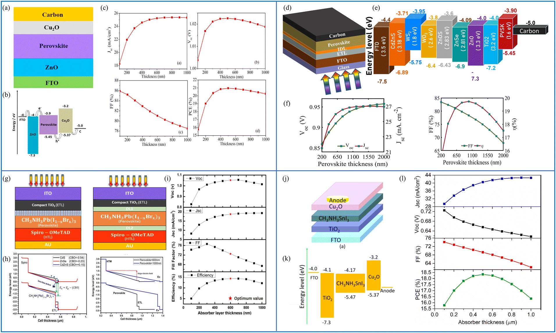 | ||
| Fig. 9 (a) Cell structure of the Cu2O HTL-based solar cell, (b) energy band diagram, and (c) cell performance parameters Jsc (mA cm−2), Voc (V), FF (%) and PCE (%). (Source: Lin et al.;142 copyright 2019 licensed under Copyright Clearance Center Inc.) (d) Cell structure of the HTL-free carbon-based perovskite device, (e) band diagram including all the ETL materials for the proposed structure, and (f) cell performance parameters Jsc (mA cm−2), Voc (V), FF (%) and PCE (%) against the absorber layer thickness from 200 nm to 2000 nm. (Source: Ijaz et al.;146 (copyright 2023 licensed under Copyright Clearance Center Inc.) (g) Schematic of the experimental and simulated devices with and without defect layers (DL1 and DL2) between the ETL and the perovskite and between the perovskite and HTL, respectively, (h) energy band diagrams of the simulated devices under different conditions, and (i) performance parameters Jsc (mA cm−2), Voc (V), FF (%) and PCE (%) of the device with an absorber thickness in the range from 100 nm to 1000 nm (source: Ahmed et al.;147 copyright 2020 licensed under the Copyright Clearance Center, Inc.). (j) Schematic of the CH3NH3SnI3-based solar cell device, (k) energy level diagram of the proposed device, and (l) PV parameters Jsc (mA cm−2), Voc (V), FF (%) and PCE (%) with respect to the varying thickness of the absorber layer from 100 to 1000 nm. (Source: Patel et al.;148 copyright 2021 licensed under the Copyright Clearance Center, Inc.) | ||
The authors in ref. 147 also simulated the CH3NH3Pb(I1−xBx)3 perovskite-based n–i–p solar cell using the SCAPS simulator. They applied carrier band offset (CBO) engineering to find the optimum performance using different ETL materials. The device assumes the ITO/TiO2/CH3NH3Pb(I1−xBx)3/Spiro-OMeTAD/Au structure, as shown in Fig. 9(g), with the energy band diagrams shown in Fig. 9(h). They evaluated the device performance with and without the inclusion of a defect layer (DL1 and DL2) between the ETL and the perovskite and between the perovskite and HTL, respectively, to compensate for the difference between the experimental and simulated device because SCAPS-1D cannot calculate 3D structures. Fig. 9(i) depicts how the device behaves when the thickness of the absorber layer is changed from 100 nm to 1000 nm, and it is shown that Jsc increases with thickness, Voc has a slow increase in the beginning which saturates and then decreases. The FF of the device decreases when absorber thickness exceeds 300 nm, and the PCE reaches the highest value for 600 nm. The device output parameters for the different ETL materials are summarised in Table 1.
| ETL material | V oc (mV) | J sc (mA cm−2) | FF (%) | PCE (%) |
|---|---|---|---|---|
| TiO2 | 1.1696 | 20.6580 | 83.15 | 20.09 |
| ZnO | 1.1695 | 20.6530 | 83.12 | 20.90 |
| ZnSe | 1.1681 | 20.6173 | 82.76 | 19.93 |
| ZnOS | 1.2061 | 20.7057 | 88.28 | 22.05 |
| CdS | 1.1546 | 20.5167 | 80.87 | 19.16 |
| CdZnS | 1.2436 | 23.3594 | 86.29 | 25.20 |
| PCBM | 1.2043 | 20.3143 | 87.93 | 21.51 |
| SnO2 | 1.1861 | 20.6541 | 86.56 | 21.21 |
The results clearly show that the highest performance is achieved when CdZnS is used as the ETL. The Jsc, Voc, FF (%) and PCE (%) are, respectively, 23.35 mA cm−2, 1.24 V, 86.29% and 25.20%. A lead-free planar heterojunction CH3NH3SnI3-based solar cell device was simulated and characterized using SCAPS in ref. 148. The working point for the device simulation was set to 300 K, and AM1.5G under 1 Sun illumination. The active region of the device was 1 cm2. The device schematic is included in Fig. 9(j), where CuO2 is used as the HTL material and TiO2 as the ETL. Fig. 9(k) shows the energy level diagram of the materials used in the device, and the effect of changing the thickness of the absorber layer (between 100 and 1000 nm) on the device performance parameters is shown in Fig. 9(l). Jsc is shown to increase up to 700 nm, whereas Voc is seen to decrease because of the recombination of free carriers in thicker absorber layers. As the absorber thickness is increased, FF decreases monotonically due to series resistance, and the PCE reaches a maximum value of 18.36% at 500 nm. The mobility, thickness, absorption coefficient of the perovskite layer and defect density, for example, have a direct impact on the device's performance. The authors have realized the overall optimization of the presented device having parameters as Jsc = 40.14 mA cm−2, Voc = 0.93 V, FF = 75.78%, and PCE = 28.39%.
5. Organic solar cells (OSCs)
OSCs featuring organic polymer molecules are an innovative replacement for traditional inorganic photovoltaic technologies that offer the potential for large-area applications and flexible energy generation. These organic molecules aim to enhance the charge transport and light absorption in solar cells.151 OSCs have gained importance based on the fact that they may become an alternative to their inorganic counterparts in conventional solar cells owing to their cost-effective, environmentally friendly, lightweight and abundant nature.16 Low-temperature manufacturing, colour tuning, flexibility and deposition on various substrates are additional characteristics offered by OSCs.152 These cells have successfully reached to PCE of more than 1.8% over the past decade,22,153,154 hence paving their way for their commercialization. Their performance can be improved further with a clear understanding of the nanostructure morphology, device structure and material optimization.5.1 Design and working principle of OSCs
By analogy to conventional solar cells, the architecture of OSCs is also made up of different layers stacked on each other, where each layer has a specific function. A comparison of the advanced designs of OSCs is shown in Fig. 10(a), where the simplest OSC is made up of a single active layer between the hole- and electron-collecting layers (i.e., cathode and anode). In an attempt to improve the PCE and to reduce the losses, i.e., electron diffusion and the loss of charge carriers via recombination, several modifications of the active layer were introduced, leading to bilayer heterojunction (BHJ) OSCs and the next challenge, i.e., the production of an increased interface area between the acceptor and donor layers because they lower the exciton diffusion and help to overcome recombination losses. This was achieved via the incorporation of donor and acceptor materials, which act as the active layers. These advancements led to a breakthrough in the PCE of OSCs.155 To increase the stability of BHJ OSCs, factors such as the interfacial engineering of buffer layers, device encapsulation, alternative materials for electrodes, and the morphology of the active layers should be explored in detail.156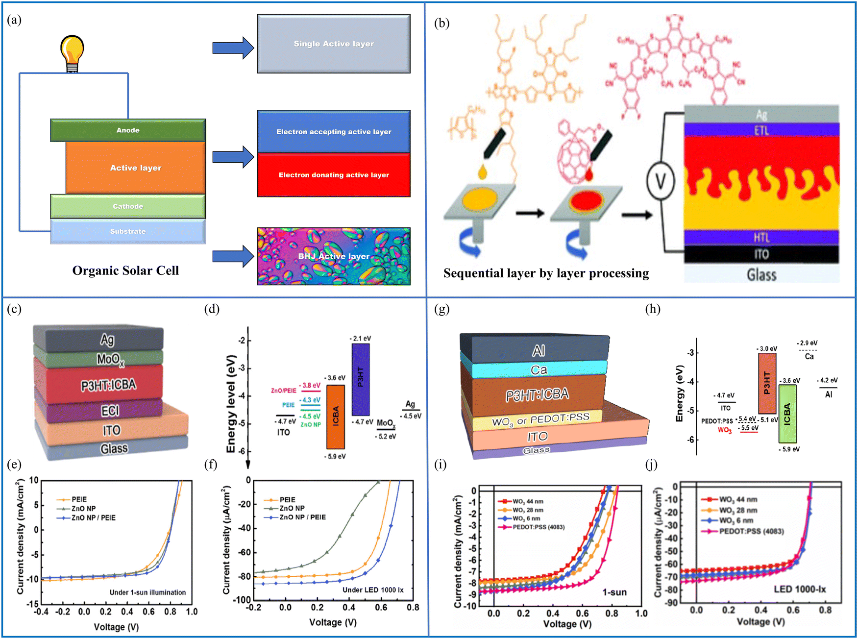 | ||
| Fig. 10 (a) Schematic diagram of an OSC with a single active layer structure, a bulk heterojunction structure and bi-layer heterojunction structure, and (b) sequential layer-by-layer processing of an OSC. Reproduced from ref. 157 with permission from the Chinese Chemical Society (CCS), Institute of Chemistry of Chinese Academy of Sciences (IC), and the Royal Society of Chemistry. (c) An inverted organic cell structure proposed for indoor use, featuring a layer of P3HT:ICBA as the absorber material, (d) energy band diagram of the cell, (e) J–V analysis of the cell under 1-Sun illumination, and (f) J–V characteristics of the cell under a 1000-lx light-emitting diode (source: Shin et al.;158 copyright 2019 licensed under the Copyright Clearance Center, Inc.). (g) Device structure with the WO3 HCL, (h) schematic of the energy levels in an OPV device based on the WO3 HCL, (i) J–V analysis of the cell under 1-Sun illumination (100 mW cm−2), and (j) current–voltage (J–V) characteristics of the cell analyzed under a light-emitting diode illumination source at an intensity of 1000-lx (0.28 mW cm−2) (source: Kimet et al.;159 copyright 2020 licensed under Copyright Clearance Center, Inc.). | ||
In OSCs, the absorption of photons takes place in organic photo-active layers, leading to the excitation of electrons from the highest occupied molecular orbital (HOMO) to the lowest unoccupied molecular orbital (LUMO), successively forming excitons. Afterwards, these excitons diffuse slowly in separate charge carriers where the electrons are gathered by the anode while the holes remain on the organic molecule. The difference in WF between the anode and cathode makes the transportation of charge carriers possible. The holes move towards the electrode with a positive large WF, and the electrons move towards the electrode with a negative small WF. If an external potential difference is applied, charge begins to flow between these two electrodes, resulting in the flow of an electric current. For the successful operation of an OSC, the major considerations include the optimization of exciton generation, the absorption of light, diffusion of the electron–hole pair towards the active interface, charge transport, charge separation and, eventually, charge collection.160
5.2 Fabrication techniques for OSCs
OSCs are made either by thermal evaporation or wet processing.161 Some other common methods include inkjet printing,162 magnetron sputtering,160 solvent-based fabrication,163,164 sequential deposition or the layer-by-layer technique,165 where the layer-by-layer method can also be used to make bilayer heterojunction OSCs (Fig. 10(b)).157 In essence, dilute mixtures of electron acceptor and donor materials are prepared by dissolving then in a volatile solvent, and thin films are produced by coating these mixtures onto a substrate. When the solvent evaporates, an active layer of two uniform regions of the electron-acceptor and electron-donor is formed. This active layer is then placed between a cathode and an anode. Different morphologies in the active layer can be formed using various processing conditions, methods of coating and types of substrate. The morphology has a directly effects on the PCE of OSCs.166 In ref. 158, atomic force microscopy (AFM), ultraviolet-visible (UV-vis) spectroscopy and a Kelvin probe were each used to examine the morphological, optical, electrical and chemical features of the electron collecting interlayers (ECIs). The ECIs were used to create inverted poly(3-hexylthiophene-2,5-diyl):indene-C60 bis-adduct (P3HT:ICBA) OPVs. Using poly(ethyleneimine)-ethoxylated (PEIE) to reducing the WF of the ECI, OPVs with the PEIE modification demonstrated a remarkable indoor performance. In particular, OPVs containing ZnO NPs/PEIE ECI produced the maximum efficiency, which was roughly 14.1% under a 1000-lx light-emitting diode bulb.5.3 Simulation and mathematical modelling of organic solar cells
In this article, we have established the fact that simulation and mathematical modelling have been crucial for the design and optimization of OSCs without the need for expensive and time-consuming experimental studies. In general, the lack of a full understanding of their complex optoelectronic properties limits the design performance. These computational techniques enable researchers to foresee the functioning of the devices under various operating parameters while identifying ways for advancing the PCEs. They provide a means of gaining insight into the underlying physics of organic solar cells, and to optimize their design for improved efficiency.In the framework of OSCs, simulations are used to model a number of phenomena, mainly charge transport and recombination, light absorption and scattering, and the impact of external factors such as the temperature and illumination intensity on the cell's performance. Several simulation methods exist that have so far been used for studying OSCs, and which have aided in exploring new materials and device architectures for OSCs to improve their efficiency. The drift-diffusion model describes the movement of charge carriers within the cell and their interactions with the material, and has been applied to predict the cell's current–voltage characteristics while identifying the factors that limit their efficiency.167 Similarly, the Monte Carlo method describes the random movement of charge carriers within the cell and has been applied to predict the impact of defects and impurities on the performance of the cell, as well as to identify strategies for reducing the footprint of the device.168
In addition to simulation methods, various mathematical models help to describe the optoelectronic properties of OSCs. The response of the solar cell is analysed beforehand, according to variations in the electrical and optical properties or some external stimuli in the system. Some common mathematical models used in the study of OSCs include the Shockley–Read–Hall model,169,170 which describes the recombination of charge carriers within the cell, and the Marcus theory, which describes the transfer of electronic excitation energy within the cell.171
As the field of organic solar cells has continued to grow and evolve, it is most likely that these methods will play an increasingly impressive role in the design and optimization of these devices. The Lumerical-FDTD-based performance evaluation of an indoor organic cell is presented in ref. 158. Poly(ethyleneimine)-ethoxylated (PEIE), and zinc oxide (ZnO) nanoparticles (NPs) were used as separate electron-collecting interlayers (ECIs), and the performance was unsatisfactory when analyzed, but when the ZnO NPs and PEIE were combined as an ECI, the performance was improved. The presented cell that contains the ZnO NPs/PEIE ECI produced a maximum efficiency of 14.1% under a luminance with a 1000-lx bulb. The authors used the cell in an inverted configuration to achieve enhanced air stability while simultaneously avoiding the use of reactive and acidic components. A schematic layout of the device, including the chemical composition of the different layers, is exhibited in Fig. 10(c). The band diagram containing the different components of the OSC can be seen in Fig. 10(d). The J–V characteristics of the OSC are shown in Fig. 10(e) under 1-Sun illumination, where the device approaches a PCE of 4.3 ± 0.1% when the ECI material is PEIE, it is 4.6 ± 0.2% when the ZnO NPs are used as the ECI, and it improved to 5.2 ± 0.1% when the combined PEIE/ZnO NPs were used as the ECI material. The J–V characteristics of the proposed device under indoor lighting conditions of 1000-lx are shown in Fig. 10(f). The solar cell has a PCE of 12.4 ± 0.2% when the ECI material is PEIE, it is 5.6 ± 0.1% when the ZnO NPs are used as the ECI, and it improved to 14.1 ± 0.3% when the combined PEIE/ZnO NPs were used as the ECI material.
Another indoor design is presented in ref. 159 to assess the photovoltaic properties under indoor settings by changing the WO3 layer thickness. OSCs with a composition of ITO/WO3/P3HT:ICBA/Ca/Al were designed, as shown in Fig. 10(g). The performance of these OPVs was compared with the operation of the baseline OPV that has a PEDOT:PSS layer. The standard OPV energy level diagram is depicted in Fig. 10(h). The sample J–V curves were acquired in the dark and under 1-Sun illumination (IL = 100 mW cm−2) for the PEDOT:PSS and WO3 HCIs at various thicknesses, and the results are shown in Fig. 10(i).
The PV characteristics of each device are summarised in Table 2. The OPV devices with 6-, 28-, and 44-nm-thick WO3 HCIs demonstrated a comparable performance under one-Sun illumination. Under one Sun illumination, the 6- and 28-nm-thick WO3 HCIs made OPV solar cells that demonstrated a comparable performance. For the devices with 6-, 28-, and 44-nm-thick WO3 HCIs, the Voc values were 0.781 ± 0.014, 0.789 ± 0.016, and 0.789 ± 0.79 V, while the Jsc (μA cm−2) values were 8.3 ± 0.5, 8.29 ± 0.2, and 7.39 ± 0.2 mA cm−2, respectively. The photovoltaic (OPV) device with a 28-nmnthick WO3 HCI demonstrated the most significant conversion efficiency of 3.90 ± 0.30%. By contrast, the OPV device with the 44-nm-thick WO3 HCI demonstrated the lowest Jsc of 7.40 ± 0.20 mA cm−2, a fill factor (FF) of 57.0% ± 2.6%, and a PCE of 3.30% ± 0.10%. The inferior PV parameters observed in the second configuration can be ascribed to its greater thickness, leading to lower charge-collection efficiency and increased charge recombination.
| HCL | HCL thickness (nm) | V oc (V) | J sc (mA cm−2) | FF (%) | PCE (%) |
|---|---|---|---|---|---|
| WO3 | 44 | 784 ± 8 | 7.4 ± 0.2 | 57.0 ± 2.6 | 3.3 ± 0.1 |
| 28 | 790 ± 7 | 8.3 ± 0.2 | 59.0 ± 1.5 | 3.9 ± 0.3 | |
| 6 | 781 ± 14 | 8.3 ± 0.5 | 55.2 ± 1.7 | 3.6 ± 0.2 | |
| PEDOT:PSS(4083) | 25 | 837 ± 3 | 8.3 ± 0.5 | 68.1 ± 1.7 | 4.9 ± 0.2 |
Conversely, the OSC featuring the PEDOT:PSS HCI as the reference exhibited a marginally better performance. It recorded a Voc, Jsc, FF, and PCE of 837 ± 3 V, 8.3 ± 0.5 mA cm−2, 68.10 ± 1.70%, and 4.90 ± 0.20%, respectively. It is possible that this is due to the superior electrical conductivity of the PEDOT:PSS HCI.172Fig. 10(j) shows the current–voltage analysis of the cell illuminated using a 1000 lx light-emitting diode source (0.280 mW cm−2), and the average photovoltaic parameters of 10 OSCs using the light-emitting diode source are presented in Table 3. Under the same conditions, the OSC with the PEDOT:PSS HCI showed a reasonable performance that was comparable to the other device. Its Voc and Jsc values were 702 ± 4 V and 74.6 ± 1.7 mA cm−2, respectively, but it had a slightly lower FF value of 67.7 ± 1.3%. Consequently, this resulted in the highest PCE of 12.7 ± 0.2%. The change in the Jsc values among the devices was only minor, indicating that Jsc is not influenced greatly by Rs under low light conditions, as explained in ref. 159. Since there is a direct relationship between the light intensity and Jsc, and the light of the 1000-lx light-emitting diode used is significantly lower in power compared with that of standard 1-Sun illumination, the Jsc value dropped from approximately 8.40 mA cm−2 under light-emitting diode illumination to 70 mA cm−2. The Voc values for the OSCs were affected by the different light sources used (1-Sun and light-emitting diode illumination), as indicated in ref. 159. Since Voc is logarithmically related to Jsc, a decrease of approximately 100 to 200 mV was recorded upon reducing the light intensity from 100 to 0.28 mW cm−2.
| HCL | HCL thickness (nm) | V oc (V) | J sc (mA cm−2) | FF (%) | PCE (%) |
|---|---|---|---|---|---|
| WO3 | 44 | 712 ± 9 | 63.1 ± 2.3 | 74.4 ± 0.4 | 11.9 ± 0.2 |
| 28 | 713 ± 3 | 68.2 ± 1.6 | 774.9 ± 0.4 | 13.0 ± 0.3 | |
| 6 | 711 ± 4 | 66.7 ± 2.1 | 73.7 ± 0.8 | 12.5 ± 0.4 | |
| PEDOT:PSS(4083) | 25 | 702 ± 4 | 74.6 ± 1.7 | 67.7 ± 1.3 | 12.7 ± 0.2 |
A finite-difference time-domain (FDTD) simulation was used to identify the ECI-dependent (Jsc) change under light-emitting diode illumination. Although the EQE measurement is a suitable method for estimating the Jsc values, this study did not investigate it under weak light-emitting diode light illumination. In Fig. 11(a) under light-emitting diode illumination, using FDTD simulations, the power absorption proportions were examined for all the devices. Below wavelengths of 550 nm, the device using the PEIE ECI exhibited a marginally higher power absorption ratio, while there was no noticeable variation between the two alternative cells using zinc oxide NPs. The simulated results obtained from FDTD essentially consist of optical-effects-focused computation that ignores other electrical effects such as the presence of electrical resistance at junctions and in the bulk form.173,174 The solar cell construction was subjected to 2D simulations using Lumerical, an FDTD solution programme. The distribution of the normalised E-field caused by light inside the solar cell structure was calculated using FDTD simulations.
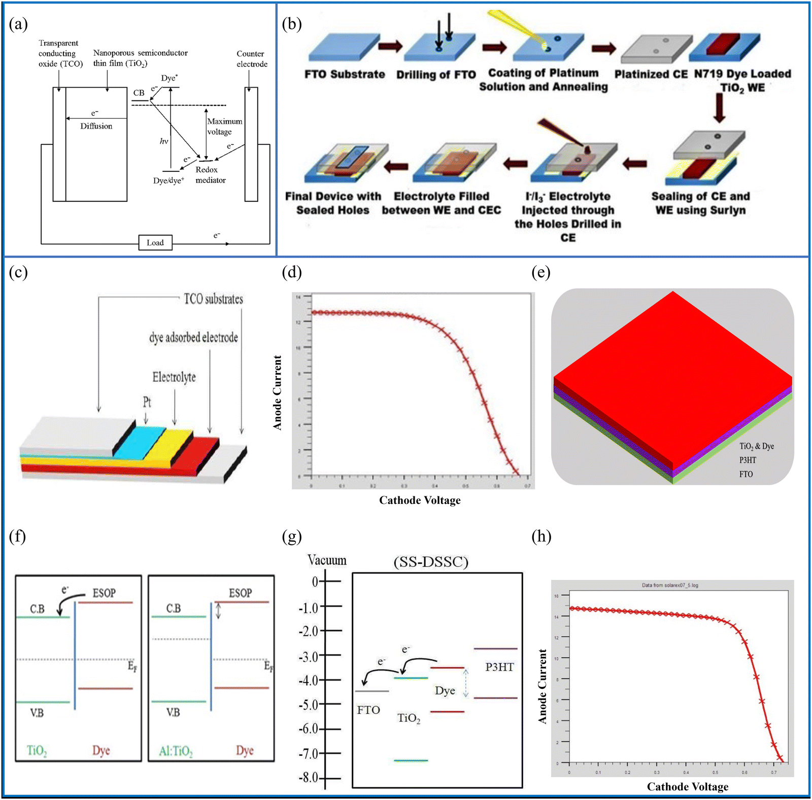 | ||
| Fig. 11 (a) Schematic diagram containing the working principle of the DSSC. (b) Schematic of the step-wise fabrication of DSSCs (reprinted under terms and conditions of the Creative Commons Attribution 4.0 International Public License. Source: Roy et al.;175 ACS, J. Phys. Chem. C, 2019). (c) Illustration of a DSSC with different layers, (d) performance of the DSSC photocurrent density–voltage (J–V) system, (e) SS-FTO/TiO2-Dye/P3HT/Pt:FTO DSSC's structural design, (f) energy level diagram demonstrating charge transfer from the dye to TiO2, (g) samples of the SS-DSSC band diagrams using P3HT and explanations of how the ESOP of the dye, the HOMO of P3HT, and the electrolyte differ from one another (dashed lines), and (h) J–V analysis of the FTO/TiO2-dye/P3HT/platinum-doped FTO structure SS-DSSC (source: Mehrabian et al.;176 copyright 2018 licensed under Copyright Clearance Center, Inc.). | ||
6. Dye sensitized solar cells (DSSCs)
DSSCs are thin-film solar cells that consist primarily of a layer of TiO2 film covered with a charge transfer dye, whose photosensitivity stimulates the absorption of solar energy.177 There has been extensive research carried out on DSSCs for around two decades because they are inexpensive, easily produced, have low toxicity and an effective performance.178 They also have the ability to work under low-light conditions.179,180 Their efficiencies have increased from 5% to 15% with the inclusion of perovskite-based mesoporous solar cell advancements.181 In addition, there are different types of DSSCs, such as liquid electrolyte-based DSSCs,182 quasi solid-state DSSCs,183,184 quantum dot sensitised solar cells185 and flexible DSSCs.186 DSSCs also have the ability to be printed on flexible substrates, they can work in diffuse light and fluorescent light, meaning that they can be used indoors as well.187 Attempts to improve the conversion efficiency have resulted in a variety of DSSC designs. In this connection, tandem systems have assisted in enhancing the overall efficiency of DSSCs, for example, n–n tandem DSSCs, p–n tandem DSSCs and DSSCs in tandem with other solar cells are possible variants of such tandem systems.188 The aim of tandem systems is to improve the absorption capability so that the full solar spectrum is covered. Lü et al. formed a GaInP/GaAs/InGaAs/Ge 4-J tandem solar cell, and they recorded a PCE of 33.9% under AM0 illumination.1896.1 Design and working principle of DSSCs
The purpose of DSSCs, similar to all of the SCs previously outlined, is to transform solar energy into electrical current. Fig. 11(a) shows the step-by-step working mechanism of a DSSC. A conductive glass is used as the substrate, which is mainly ITO or FTO. A thin layer (5–30 microns) of nanocrystalline TiO2 coated on the glass substrate acts as an electrode. The electrode is further coated with a layer of charge transfer dye. When incident light falls on the dye molecules they absorb it and their electrons go into excited states. These excited negatively charged carriers go to the mesoporous TiO2 film which acts as an anode and promotes conduction. When the dye loses an electron the electrolyte restores it by donating one. This electrolyte acts as a redox mediator, which is an organic material that chiefly contains iodide and tri-iodide. The electron donation leads another electron to move towards the oxide film. During this course of action, the iodide is regenerated by the tri-iodide through its reduction at the other electrode via an external load. In short, electric power is generated without complete chemical transformation.190 The selection of the dye depends mainly on the type of DSSC. Liquid electrolyte-based DSSCs use iodide/tri-iodide dyes, whereas quasi-solid-state DSSCs use a hole transport material and polymer gel dyes. A reasonable dye requires a good absorption to match the solar spectrum range, good stability and the ability to be uniformly deposited on the semiconductor electrode. Moreover, its redox potential should support the regeneration reaction with a redox mediator.1916.2 Fabrication techniques for DSSCs
The thermal CVD growth of zinc oxide (ZnO) nanostructures can be used to fabricate DSSCs.192 O'Regan et al. synthesized n-type ZnO DSSCs using electrochemical deposition.193 CuSCN DSSCs can also be fabricated using the chemical solution method.194 Cd-doped ZnO DSSCs were synthesised using the solvothermal method.195 Layer-by-layer assembly can also be used to fabricate DSSCs.196 In another route, DSSCs were manufactured using TiO2-coated multi-walled carbon nanotubes (CNTs) due to their chemical stability and excellent electrical conductivity characteristics. CNTs in DSSCs reduce the series resistance while improving the solar cell performance.197 Roy et al. fabricated DSSCs by changing the TiO2 thickness, where the main factors for determining colour comfort are the color rendering index (CRI) and the correlated color temperature (CCT), which were measured using the observed visible transmittance. A sandwich-like cell was formed by joining the TiO2 coated electrode and a Pt-coated counter electrode (CE). A hot-melt square gasket made of the Surlyn thermoplastic sealant with a thickness of 30 μm was adjusted so that its internal size was consistent with the working electrode's active cell region. While the dye-sensitized metal oxide and the Pt-coated conducting side remained in a side-to-side layout, the CE was placed on the working electrode (WE). To make the final sealed DSSC device, the electrolyte was carefully poured across the hole of the CE. Using various layers of the TiO2 paste, transparent TiO2 films with thicknesses of 3.5, 6 and 10 μm were coated on FTO glass. The step-wise illustration of the manufactured cell configuration is displayed in Fig. 11(b). The fabricated solar cell exhibited PCE values of 2.51, 4.49 and 5.93% under 1 Sum AM 1.5G illumination.1756.3 Simulation and mathematical modelling of DSSCs
The simulation and mathematical modelling of DSSCs typically involves the use of various software tools, such as MATLAB, COMSOL, or SCAPS-DSSC, which can simulate the different mechanisms taking place while the cell operates, including the absorption of light by the dye, the charge carriers, and the movement of electrons through the cell. The simulation of DSSCs typically begins by creating a mathematical model of the electrodes, the electrolyte and the dye that are used for fabrication of the cell. These models are then used to simulate the behaviour of the cell under different operating conditions, including different intensities and temperatures of sunlight. The simulation can also be used to optimize the design of the cell, such as by tuning the thickness of the electrodes or the concentration of the dye, to improve its efficiency. In a DSSC, the sensitizers convert photons into excitons by acting as absorber components, whether they be quantum dots or ruthenium dyes. Due to the disparity in electron affinities, the excitons move towards the interface between the dye and semiconductor, where they separate into independent electrons and holes. For this process to occur, the energy of the semiconductor conduction band should be more than the energy level of the dye's LUMO.In ref. 176, simulations were carried out to replace the liquid electrolyte with a semiconductor solid layer Fig. 11(c) and (f) show the schematic diagram and the band diagram of a DSSC, respectively. The SILVACO TCAD software was employed to simulate a DSSC that featured an FTO/TiO2-Dye/Electrolyte/Pt-doped FTO structure. Subsequently, the interfacial charge transfer mechanism was enhanced by substituting the TiO2 layer in conjunction with an aluminium-doped TiO2 layer. Using a liquid electrolyte containing iodide/tri-iodide redox couples and organic solvents with volatile compounds can lead to significant issues, which include electrolyte leakage, electrode corrosion, degradation of the cell performance over time, and challenges with sealing.
Fig. 11(d) shows the photo-current density–voltage performance of the simulated DSSC featuring the FTO/TiO2 structure, subjected to AM 1.5G solar illumination at 100 mW cm−2. To overcome the shortcomings imposed by the use of liquid electrolytes, a simulation study for a solid-state dye-sensitized solar cell (SS-DSSC) was performed. The SS-DSSC uses a P3HT layer as the hole collector instead of a liquid electrolyte. The results were promising, with a record Voc of 0.67 V and a Jsc of 12.70 mA cm−2. Liquid electrolyte leakage was resolved through introduction of the solid electrolytes. The SS-DSSCs hold great promise for practical applications. The p-type semiconductor poly(3-hexylthiophene) (P3HT) exhibits a relatively high hole mobility of (10−4 to 10−3 m2 V−1 s−1)198 and has an energy bandgap of around 2 eV. Both the HOMO and the LUMO can be found in the energy range of 5 and 3 electron volts (eV) below the vacuum.
One could model a SS-DSSC with a structure comprised of an FTO substrate, a TiO2 and dye layer, a p-type polymer (P3HT) layer and a platinum-coated FTO layer. Such a simulation could demonstrate the potential for P3HT to serve as the HTL in place of an electrolyte.
The corresponding layers were 200 nm, 100 nm, and 80 nm thick. The layout of this model can be seen in Fig. 11(e). Fig. 11(h) shows the J–V analysis of this simulated SS-DSSC with the FTO/TiO2-Dye/P3HT/Pt:FTO structure under AM 1.5G sunlight illumination. The PV parameters of this configuration are Jsc is 0.73 mA cm−2, a short circuit current of 14.74 mA, an FF of 67.69%, and the PCE of this cell is 6.70%.
In an SS-DSSC, the energy gap of the excited singlet state of the p-type semiconducting polymer (P3HT) and its HOMO is less than the energy difference between excited state oxidation potential (ESOP) of the dye and the electrolyte's LUMO, as shown in comparison with a traditional DSSC in Fig. 11(f and g). The rate of photo-electron recombination increases when P3HT is used in place of the liquid electrolyte. This shows that in SS-DSSCs, the dye's ESOP electrons were unable to fully inject into the TiO2 conduction band. In other words, rather than producing the photocurrent, the holes in the HOMO of P3HT will recombine with the electrons when they travel from the dye to TiO2. Consequently, the Jsc dropped from 14.74 to 12.70 mA cm−2. In order to address concerns regarding the use of liquid electrolytes, a SS-DSSC with a P3HT HTL was simulated using the suggested model. The P3HT layer connected dye particles that are joined to TiO2, further to the CE. The findings revealed that, in comparison with a DSSC that uses liquid electrolytes, the SS-DSSC had a slightly smaller efficiency. The difference between the dye, the ESOP, the P3HT HOMO and the electrolyte resulted in an elevated carrier recombination rate, which causes a decrease in the power conversion efficiency. For additional SS-DSSC heterojunction solar modules, these simulation results may offer some encouragement.
All of the types of PV cells that differ from each other on the basis of the active layer are thoroughly discussed in this review paper and are summarized in Table 4 using particular examples. The table includes the types of cells, the materials used in the design of a particular type with their configurations and the fabrication techniques used in their manufacturing. The performance evaluation parameters are also given for each of the examples. It is noteworthy that perovskite solar cells are high-performing devices.
| Cell type | Material | Cell structure | V oc (mV) | J sc (mA cm−2) | FF (%) | PCE (%) | Fabrication technique |
|---|---|---|---|---|---|---|---|
| 2D material | PFN/PTB7:WSe2:PCBM199 | Glass/ITO/PFN/PTB7:WSe2:PCBM/MoO3:A | 0.731 | 17.69 | 71.7 | 9.28 | Three step cleaning process |
| AgNW-MoS2/n-MoS2200 | Glass/AgNW-MoS2/n-MoS2/PBDTTT-CT:PCBM/p-MoS2/Ag | 0.76 | 15.66 | 67 | 8 | Sol–gel method | |
| Graphene/PEDOT:PSS201 | Glass/graphene/PEDOT:PSS/WO3/SMPV1:PC71BM/ZnO/PEDOT:PSS/PTTBDT-FTT:PC71 BM/Ca/Al | 1.56 | 8.45 | 64.32 | 8.84 | Electron beam lithography | |
| Quantum dots | CdS202 | FTO/TiO2/CdS/ZnS/S2−–Sn2−/FGO Cu2S/FTO | 0.496 | 7.2 | 46 | 1.63 | SILAR process |
| CdS–Mn202 | FTO/TiO2/CdS–Mn/ZnS/S2−–Sn2 −/FGO-Cu2S/FTO | 0.583 | 8.9 | 49 | 2.52 | SILAR process | |
| CdSe203 | TiO2/CdSe-MPA/ZnS/S2−–Sn2 −/Cu2S/Brass | 0.561 | 16.96 | 56 | 5.42 | A post-synthesis assembly approach | |
| CdTe/CdSe204 | TiO2/CdS/CdSe/ZnS/S2−–Sn2 −/Pt/FTO | 0.606 | 19.59 | 56 | 6.76 | Non-injection high-temperature pyrolysis route | |
| Perovskites | MAPbI3205 | TiO2/ZrO2/(5-AVA)x(MA)1−xPbI3/C (unsealed) | 1.07 | 21.60 | 76.8 | 17.77 | Solution synthesis |
| CH3NH3PbI3206 | Glass/ITO/CH3NH3PbI3 | 0.86 | 19.46 | 67 | 11.21 | Electro deposition | |
| CH3NH3PbI3207 | ITO/Cu:NiOx/CH3NH3PbI3/Ag | 1.05 | 20.60 | 77 | 17.74 | Combustion method | |
| Organic | q-BHJ in toluene14 | ITO/ZnO/active layer/PFN-Br/Ag | 0.86 | 21.68 | 70 | 13.08 | Green fabrication |
| PTVT-T:ITCC208 | ITO/PTVT-T:ITCC/Ag | 1.08 | 14.30 | 62.06 | 9.60 | ITCC as the acceptor | |
| PEDOT:PSS159 | ITO/WO3/P3HT:ICBA/Ca/Al | 0.71 | 68.1 | 75 | 13.0 | Thermal evaporation | |
| Dye sensitized | TiO2209 | TiO2/TCO/C4H10O | 0.74 | 20.9 | 72 | 11.1 | Screen-printing |
| ZnO210 | SnO2:F-coated (FTO)/ZnO/N719 | 0.62 | 18.11 | 59 | 6.6 | Squeegee method | |
| MgO/SnO2211 | hITO/SnO2/MgO/FTO | 0.75 | 14.21 | 67 | 7.2 | Surface spray | |
7. Future perspective
Researchers are exploiting the exceptional properties of all of the aforementioned variants of solar cell technology to explore new ventures in this domain, and the future of this technology lies in the formation of multi-junction solar cells that are composed of different layers of these favourable materials. The combination of the discussed solar cells may also lead to the formation of heterojunction solar cells that show enhanced photovoltaic properties or characteristics compared with their individual counterparts. A demonstration of such a 2D/3D bulk heterojunction solar cell that consists of a 2D/3D inorganic perovskite has been shown by Kang et al.212 Similarly, a heterojunction solar cell of 2D materials based PSCs and OSCs,213 quantum dot-based PSCs,214 graphene quantum dot-based DSSCs,215 and organic sensitizers for DSSCs216 have been reported in the literature.8. Conclusion
In this review paper, we have set forth a brief overview of the most advanced generation of solar cell technology, i.e., fourth-generation solar cells, that consist mainly of 2D material-based solar cells, quantum dot-based solar cells, perovskite solar cells, organic solar cells and dye-sensitised solar cells. The paper aims for readers to become well acquainted with the working principles, design parameters, fabrication, simulation and mathematical modelling of the aforementioned SCs as they have revolutionized solar cell technology. They currently offer the highest achievable efficiencies along with compact designs, flexibility, environmental friendliness and stability. Using the combined features of these solar cells, researchers in this area may formulate even more efficient designs to offer an extensive set of advantages compared with current solar cell technologies. Further advances in the field of solar cell research are anticipated with the discovery of novel materials, ease of fabrication, device designs, and a deeper understanding of the physics underlying the performance characteristics of solar cells.Conflicts of interest
There are no conflicts to declare.Notes and references
- F. Saeed and A. Zohaib, Eng. Proc., 2022, 11, 35 Search PubMed.
- B. H. Hamadani, Appl. Phys. Lett., 2020, 117, 043904 CrossRef CAS PubMed.
- R. Corkish, in Encyclopedia of Energy, ed. C. J. Cleveland, Elsevier, New York, 2004, pp. 545–557 Search PubMed.
- L. M. Fraas, Low-cost solar electric power, Springer, 2014 Search PubMed.
- T. Zhang, M. Wang and H. Yang, Energies, 2018, 11, 3157 CrossRef CAS.
- B. Salhi, Materials, 2022, 15, 1908 CrossRef CAS PubMed.
- W. Shockley and H. J. Queisser, J. Appl. Phys., 1961, 32, 510–519 CrossRef CAS.
- J. A. Hogan, J. D. Lakey and J. D. Lakey, Duration and bandwidth limiting: prolate functions, sampling, and applications, Springer, 2012 Search PubMed.
- V. Muteri, Cellura, D. Curto, Franzitta, S. Longo, Mistretta and M. L. Parisi, Energies, 2020, 13, 252 CrossRef CAS.
- K. Ahmad, S. Naqvi and S. Bibi Jaffri, Rev. Inorg. Chem., 2020 DOI:10.1515/revic-2020-0009.
- Z. Li, Y. Zhao, X. Wang, Y. Sun, Z. Zhao, Y. Li, H. Zhou and Q. Chen, Joule, 2018, 2, 1559–1572 CrossRef CAS.
- N. S. Kumar and K. C. B. Naidu, J. Materiomics, 2021, 7, 940–956 CrossRef.
- X. Zhao, T. Liu, W. Shi, X. Hou and T. J. S. Dennis, Nanoscale, 2019, 11, 2453–2459 RSC.
- D. Wang, H. Liu, Y. Li, G. Zhou, L. Zhan, H. Zhu, X. Lu, H. Chen and C.-Z. Li, Joule, 2021, 5, 945–957 CrossRef CAS.
- M. Riede, D. Spoltore and K. Leo, Adv. Energy Mater., 2021, 11, 2002653 CrossRef CAS.
- L. X. Chen, ACS Energy Lett., 2019, 4(10), 2537–2539 CrossRef CAS.
- S. A. Gevorgyan, N. Espinosa, L. Ciammaruchi, B. Roth, F. Livi, S. Tsopanidis, S. Züfle, S. Queirós, A. Gregori and G. A. D. R. Benatto, et al. , Adv. Energy Mater., 2016, 6, 1600910 CrossRef.
- F.-A. Kauffer, C. Merlin, L. Balan and R. Schneider, J. Hazard. Mater., 2014, 268, 246–255 CrossRef CAS PubMed.
- T.-I. Razika, Handbook of Nanoelectrochemistry, 2015, pp. 1–18 Search PubMed.
- M. A. Iqbal, M. Malik, W. Shahid, S. Z. U. Din, N. Anwar, M. Ikram and F. Idrees, Materials for Photovoltaics: Overview, Generations, Recent Advancements and Future Prospects, in Thin Films Photovoltaics, IntechOpen, London, 2022, vol. 5 Search PubMed.
- J. Pastuszak and P. Wegierek, Materials, 2022, 15, 5542 CrossRef CAS PubMed.
- N. Nrel, National Renewable Energy Laboratory, Golden, Colorado, 2019 Search PubMed.
- S. Das, D. Pandey, J. Thomas and T. Roy, Adv. Mater., 2019, 31, 1802722 CrossRef PubMed.
- M. K. Singh, P. V. Shinde, P. Singh and P. K. Tyagi, Solar Cells-Theory, Materials and Recent Advances, IntechOpen, 2021 Search PubMed.
- E. Muchuweni, B. S. Martincigh and V. O. Nyamori, Int. J. Energy Res., 2021, 45, 6518–6549 CrossRef CAS.
- Z. Pan, H. Gu, M.-T. Wu, Y. Li and Y. Chen, Opt. Mater. Express, 2012, 2, 814–824 CrossRef CAS.
- W. Wu, H. Wu, M. Zhong and S. Guo, ACS Omega, 2019, 4, 16159–16165 CrossRef CAS PubMed.
- Y. Xiang, L. Xin, J. Hu, C. Li, J. Qi, Y. Hou and X. Wei, Crystals, 2021, 11, 47 CrossRef CAS.
- S. F. Adil, M. Khan and D. Kalpana, Multifunctional Photocatalytic Materials for Energy, Elsevier, 2018, pp. 127–152 Search PubMed.
- S. Paulo, E. Palomares and E. Martinez-Ferrero, Nanomaterials, 2016, 6, 157 CrossRef PubMed.
- C. Chung, Y.-K. Kim, D. Shin, S.-R. Ryoo, B. H. Hong and D.-H. Min, Acc. Chem. Res., 2013, 46, 2211–2224 CrossRef CAS PubMed.
- H. Shen, L. Zhang, M. Liu and Z. Zhang, Theranostics, 2012, 2, 283 CrossRef CAS PubMed.
- M. Sang, J. Shin, K. Kim and K. J. Yu, Nanomaterials, 2019, 9, 374 CrossRef CAS PubMed.
- P. Avouris and F. Xia, MRS Bull., 2012, 37, 1225–1234 CrossRef CAS.
- X. Leng, S. Chen, K. Yang, M. Chen, M. Shaker, E. E. Vdovin, Q. Ge, K. S. Novoselov and D. V. Andreeva, Surf. Rev. Lett., 2021, 28, 2140004 CrossRef CAS.
- T. Reiß, K. Hjelt and A. C. Ferrari, Nat. Nanotechnol., 2019, 14, 907–910 CrossRef.
- E. Inshakova, A. Inshakova and A. Goncharov, IOP Conf. Ser.: Mater. Sci. Eng., 2020, 032031 CAS.
- Q. He, S. Wu, Z. Yin and H. Zhang, Chem. Sci., 2012, 3, 1764–1772 RSC.
- K. P. Loh, S. W. Tong and J. Wu, J. Am. Chem. Soc., 2016, 138, 1095–1102 CrossRef CAS PubMed.
- A. T. Smith, A. M. LaChance, S. Zeng, B. Liu and L. Sun, Nano Mater. Sci., 2019, 1, 31–47 CrossRef.
- T. Mahmoudi, Y. Wang and Y.-B. Hahn, Nano Energy, 2018, 47, 51–65 CrossRef CAS.
- M. Bernardi, M. Palummo and J. C. Grossman, Nano Lett., 2013, 13, 3664–3670 CrossRef CAS PubMed.
- M.-L. Tsai, S.-H. Su, J.-K. Chang, D.-S. Tsai, C.-H. Chen, C.-I. Wu, L.-J. Li, L.-J. Chen and J.-H. He, ACS Nano, 2014, 8, 8317–8322 CrossRef CAS PubMed.
- D. Vikraman, A. A. Arbab, S. Hussain, N. K. Shrestha, S. H. Jeong, J. Jung, S. A. Patil and H.-S. Kim, ACS Sustainable Chem. Eng., 2019, 7, 13195–13205 CrossRef CAS.
- P. Gao, K. Ding, Y. Wang, K. Ruan, S. Diao, Q. Zhang, B. Sun and J. Jie, J. Phys. Chem. C, 2014, 118, 5164–5171 CrossRef CAS.
- K.-T. Lee, D. H. Park, H. W. Baac and S. Han, Materials, 2018, 11, 1503 CrossRef PubMed.
- C. Chakravarty, B. Mandal and P. Sarkar, J. Phys. Chem. C, 2018, 122, 15835–15842 CrossRef CAS.
- Z. Yang, M. Liu, C. Zhang, W. W. Tjiu, T. Liu and H. Peng, Angew. Chem., 2013, 125, 4088–4091 CrossRef.
- X. Miao, S. Tongay, M. K. Petterson, K. Berke, A. G. Rinzler, B. R. Appleton and A. F. Hebard, Nano Lett., 2012, 12, 2745–2750 CrossRef CAS PubMed.
- S. Das, P. Sudhagar, Y. S. Kang and W. Choi, J. Mater. Res., 2014, 29, 299–319 CrossRef CAS.
- O. Samy, S. Zeng, M. D. Birowosuto and A. El Moutaouakil, Crystals, 2021, 11, 355 CrossRef CAS.
- K. M. Islam, T. Ismael, C. Luthy, O. Kizilkaya and M. D. Escarra, ACS Appl. Mater. Interfaces, 2022, 14, 24281–24289 CrossRef CAS PubMed.
- A. Stanford and J. Tanner, Phys. Stud. Sci. Eng., 1985, 691–716 Search PubMed.
- H. Yu, C. Xin, Q. Zhang, M. Utama, L. Tong and Q. Xiong, Semiconductor Nanowires, Elsevier, 2015, pp. 29–69 Search PubMed.
- T. Soga, Nanostructured Materials for Solar Energy Conversion, Elsevier, 2006, pp. 3–43 Search PubMed.
- O. Simya, P. Radhakrishnan, A. Ashok, K. Kavitha and R. Althaf, Handbook of nanomaterials for industrial applications, 2018, pp. 751–767 Search PubMed.
- H. Li, J. Wu, Z. Yin and H. Zhang, Acc. Chem. Res., 2014, 47, 1067–1075 CrossRef CAS PubMed.
- Y. Zhang, L. Zhang and C. Zhou, Acc. Chem. Res., 2013, 46, 2329–2339 CrossRef CAS PubMed.
- Z. Cai, B. Liu, X. Zou and H.-M. Cheng, Chem. Rev., 2018, 118, 6091–6133 CrossRef CAS PubMed.
- A. Iwan and A. Chuchmała, Progress in Polymer Science, 2012, 37, 1805–1828 CrossRef CAS.
- N. Liu, P. Kim, J. H. Kim, J. H. Ye, S. Kim and C. J. Lee, ACS Nano, 2014, 8, 6902–6910 CrossRef CAS PubMed.
- X. Cai, Y. Luo, B. Liu and H.-M. Cheng, Chem. Soc. Rev., 2018, 47, 6224–6266 RSC.
- K. S. Novoselov, A. K. Geim, S. V. Morozov, D.-E. Jiang, Y. Zhang, S. V. Dubonos, I. V. Grigorieva and A. A. Firsov, Science, 2004, 306, 666–669 CrossRef CAS PubMed.
- A. K. Geim, Phys. Scr., 2012, 2012, 014003 CrossRef.
- B. Sigma-Aldrich and P. S.-A. Region, Sigma, 2018, 302, H331 Search PubMed.
- Y. Zhu, T. Cao, C. Cao, X. Ma, X. Xu and Y. Li, Nano Res., 2018, 11, 3088–3095 CrossRef CAS.
- M. B. Tahir, M. Rafique, M. S. Rafique, T. Nawaz, M. Rizwan and M. Tanveer, Nanotechnology and Photocatalysis for Environmental Applications, Elsevier, 2020, pp. 119–138 Search PubMed.
- M. Saeed, Y. Alshammari, S. A. Majeed and E. Al-Nasrallah, Molecules, 2020, 25, 3856 CrossRef CAS PubMed.
- L. Sun, G. Yuan, L. Gao, J. Yang, M. Chhowalla, M. H. Gharahcheshmeh, K. K. Gleason, Y. S. Choi, B. H. Hong and Z. Liu, Nat. Rev. Methods Primers, 2021, 1, 1–20 CrossRef.
- X. Li, W. Cai, J. An, S. Kim, J. Nah, D. Yang, R. Piner, A. Velamakanni, I. Jung and E. Tutuc, et al. , Science, 2009, 324, 1312–1314 CrossRef CAS PubMed.
- E. T. Bjerglund, M. E. P. Kristensen, S. Stambula, G. A. Botton, S. U. Pedersen and K. Daasbjerg, ACS Omega, 2017, 2, 6492–6499 CrossRef CAS PubMed.
- S. Park and R. S. Ruoff, Nat. Nanotechnol., 2009, 4, 217–224 CrossRef CAS PubMed.
- S. Stankovich, R. D. Piner, X. Chen, N. Wu, S. T. Nguyen and R. S. Ruoff, J. Mater. Chem., 2006, 16, 155–158 RSC.
- Y. Si and E. T. Samulski, Nano Lett., 2008, 8, 1679–1682 CrossRef CAS PubMed.
- X. Li, G. Zhang, X. Bai, X. Sun, X. Wang, E. Wang and H. Dai, Nat. Nanotechnol., 2008, 3, 538–542 CrossRef CAS PubMed.
- J. Kenney and G. Hwang, MATERIALS | Etching, in Encyclopedia of Electrochemical Power Sources, Elsevier, 2009 Search PubMed.
- H. Mehmood, H. Nasser, E. Özkol, T. Tauqeer, S. Hussain and R. Turan, 2017 International Conference on Engineering and Technology (ICET), 2017, pp. 1–6.
- H. Mehmood, H. Nasser, S. M. H. Zaidi, T. Tauqeer and R. Turan, Renewable Energy, 2022, 183, 188–201 CrossRef CAS.
- P. Sarker, Md. M. Rana and A. Sarkar, Modeling of graphene conductivity using FDTD in the near infrared frequency, 2016, pp. 1–4 DOI:10.1109/ICECTE.2016.7879581.
- S. Zandi, P. Saxena and N. E. Gorji, Sol. Energy, 2020, 197, 105–110 CrossRef CAS.
- M. Yu, Y. Li, Q. Cheng and S. Li, Sol. Energy, 2019, 182, 453–461 CrossRef CAS.
- S. H. Raad and Z. Atlasbaf, Sci. Rep., 2021, 11, 1–8 CrossRef PubMed.
- C. Kaouther, Study of graphene-based solar cells by simulation, Masters thesis, University of Mohamed Khider Biskra, 2021 Search PubMed.
- M. Dadashbeik, D. Fathi and M. Eskandari, Sol. Energy, 2020, 207, 917–924 CrossRef CAS.
- S. Hungyo, R. S. Dhar, K. Kumar, K. J. Singh, R. Dey and S. Bhattacharya, Microsyst. Technol., 2021, 27, 3693–3701 CrossRef CAS.
- R. R. Nair, P. Blake, A. N. Grigorenko, K. S. Novoselov, T. J. Booth, T. Stauber, N. M. Peres and A. K. Geim, Science, 2008, 320, 1308 CrossRef CAS PubMed.
- L. Isaenko and A. Yelisseyev, Semicond. Sci. Technol., 2016, 31, 123001 CrossRef.
- M. A. Cotta, ACS Appl. Nano Mater., 2020, 3, 4920–4924 CrossRef CAS.
- S. Emin, S. P. Singh, L. Han, N. Satoh and A. Islam, Sol. Energy, 2011, 85, 1264–1282 CrossRef CAS.
- M. Zia-ur Rehman, M. F. Qayyum, F. Akmal, M. A. Maqsood, M. Rizwan, M. Waqar and M. Azhar, Nanomaterials in Plants, Algae, and Microorganisms, 2018, pp. 143–174 Search PubMed.
- V. T. Chebrolu and H.-J. Kim, J. Mater. Chem. C, 2019, 7, 4911–4933 RSC.
- J. Duan, H. Zhang, Q. Tang, B. He and L. Yu, J. Mater. Chem. A, 2015, 3, 17497–17510 RSC.
- S. Kargozar, S. J. Hoseini, P. B. Milan, S. Hooshmand, H.-W. Kim and M. Mozafari, Biotechnol. J., 2020, 15, 2000117 CrossRef CAS PubMed.
- X. Zhang, P. K. Santra, L. Tian, M. B. Johansson, H. Rensmo and E. M. Johansson, ACS Nano, 2017, 11, 8478–8487 CrossRef CAS PubMed.
- X. Song, Z. Ma, L. Li, T. Tian, Y. Yan, J. Su, J. Deng and C. Xia, Sol. Energy, 2020, 196, 513–520 CrossRef CAS.
- R. Pandey, A. Khanna, K. Singh, S. K. Patel, H. Singh and J. Madan, Sol. Energy, 2020, 207, 893–902 CrossRef CAS.
- S. Rühle, M. Shalom and A. Zaban, Chem. Phys. Chem., 2010, 11, 2290–2304 CrossRef PubMed.
- H. Zhao, J. Liu, F. Vidal, A. Vomiero and F. Rosei, Nanoscale, 2018, 10, 17189–17197 RSC.
- G. S. Selopal, H. Zhao, Z. M. Wang and F. Rosei, Adv. Funct. Mater., 2020, 30, 1908762 CrossRef CAS.
- Z. Pan, H. Rao, I. Mora-Seró, J. Bisquert and X. Zhong, Chem. Soc. Rev., 2018, 47, 7659–7702 RSC.
- I. Mora-Seró and J. Bisquert, J. Phys. Chem. Lett., 2010, 1, 3046–3052 CrossRef.
- R. Vogel, K. Pohl and H. Weller, Chem. Phys. Lett., 1990, 174(3–4), 241–246 CrossRef CAS.
- P. V. Kamat, J. Phys. Chem. Lett., 2013, 4, 908–918 CrossRef CAS PubMed.
- S. Mahalingam, A. Manap, A. Omar, F. W. Low, N. Afandi, C. H. Chia and N. Abd Rahim, Renewable Sustainable Energy Rev., 2021, 144, 110999 CrossRef CAS.
- W. Wang, L. Zhao, Y. Wang, W. Xue, F. He, Y. Xie and Y. Li, J. Am. Chem. Soc., 2019, 141, 4300–4307 CrossRef CAS PubMed.
- S. W. Tabernig, L. Yuan, A. Cordaro, Z. L. Teh, Y. Gao, R. J. Patterson, A. Pusch, S. Huang and A. Polman, ACS Nano, 2022, 16, 13750–13760 CrossRef CAS PubMed.
- Y. Arakawa, Solid-State Electron., 1994, 37, 523–528 CrossRef CAS.
- V. M. Ustinov, A. E. Zhukov, A. E. Zhokov, N. A. Maleev and A. Y. Egorov, Quantum dot lasers, Oxford University Press on Demand, 2003, vol. 11 Search PubMed.
- B. D. Chernomordik, A. R. Marshall, G. F. Pach, J. M. Luther and M. C. Beard, Chem. Mater., 2017, 29, 189–198 CrossRef CAS.
- H. Mehmood, H. Nasser, T. Tauqeer and R. Turan, Renewable Energy, 2019, 143, 359–367 CrossRef CAS.
- H. Mehmood, H. Nasser, T. Tauqeer, S. Hussain, E. Ozkol and R. Turan, Int. J. Energy Res., 2018, 42, 1563–1579 CrossRef CAS.
- W. M. Lin, N. Yazdani, O. Yarema, M. Yarema, M. Liu, E. H. Sargent, T. Kirchartz and V. Wood, ACS Appl. Electron. Mater., 2021, 3, 4977–4989 CrossRef CAS.
- K. P. Bhandari, P. J. Roland, H. Mahabaduge, N. O. Haugen, C. R. Grice, S. Jeong, T. Dykstra, J. Gao and R. J. Ellingson, Sol. Energy Mater. Sol. Cells, 2013, 117, 476–482 CrossRef CAS.
- N. Janković, S. Aleksić and D. Pantić, Proceedings of Small Systems Simulation Symposium, 2012, pp. 85–92.
- M. Mehrabian, S. Dalir and H. Shokrvash, Optik, 2016, 127, 10096–10101 CrossRef CAS.
- M. Verschuuren, M. Knight, M. Megens and A. Polman, Nanotechnology, 2019, 30, 345301 CrossRef CAS PubMed.
- C.-H. M. Chuang, P. R. Brown, V. Bulović and M. G. Bawendi, Nat. Mater., 2014, 13, 796–801 CrossRef CAS PubMed.
- V. Wood and V. Bulović, Nano Rev., 2010, 1, 5202 CrossRef PubMed.
- E. A. Katz, Helv. Chim. Acta, 2020, 103, e2000061 CrossRef CAS.
- G. Li, Advanced Nanomaterials for Solar Cells and Light Emitting Diodes, Elsevier, 2019, pp. 305–341 Search PubMed.
- A. Nande, S. Raut and S. Dhoble, Energy Materials, Elsevier, 2021, pp. 249–281 Search PubMed.
- W. Arpavate, K. Roongraung and S. Chuangchote, Green Sustainable Process for Chemical and Environmental Engineering and Science, Elsevier, 2021, pp. 189–203 Search PubMed.
- T. T. Dang, T. L. A. Nguyen, K. B. Ansari, V. H. Nguyen, N. T. Binh, T. T. N. Phan, T. H. Pham, D. T. T. Hang, P. N. Amaniampong and E. Kwao-Boateng, et al., Nanostructured Photocatalysts, 2021, pp. 169–216 Search PubMed.
- D. Alderton, S. A. Elias, S. G. Lucas, T. M. Kusky and L. Wang, Encyclopedia of geology, 2021 Search PubMed.
- N.-G. Park, Mater. Today, 2015, 18, 65–72 CrossRef CAS.
- S. K. Sahoo, B. Manoharan and N. Sivakumar, Perovskite Photovoltaics, Elsevier, 2018, pp. 1–24 Search PubMed.
- A. W. Faridi, M. Imran, G. H. Tariq, S. Ullah, S. F. Noor, S. Ansar and F. Sher, Ind. Eng. Chem. Res., 2023, 62(11), 4494–4502 CrossRef CAS PubMed.
- S. Bello, A. Urwick, F. Bastianini, A. J. Nedoma and A. Dunbar, Energy Rep., 2022, 8, 89–106 CrossRef.
- H. Röhm, T. Leonhard, A. D. Schulz, S. Wagner, M. J. Hoffmann and A. Colsmann, Adv. Mater., 2019, 31, 1806661 CrossRef PubMed.
- H. Li, F. Li, Z. Shen, S.-T. Han, J. Chen, C. Dong, C. Chen, Y. Zhou and M. Wang, Nano Today, 2021, 37, 101062 CrossRef CAS.
- P. R. Varma, Perovskite Photovoltaics, Elsevier, 2018, pp. 197–229 Search PubMed.
- Z.-H. Zheng, H.-B. Lan, Z.-H. Su, H.-X. Peng, J.-T. Luo, G.-X. Liang and P. Fan, Sci. Rep., 2019, 9, 17422 CrossRef PubMed.
- Y. Zhou, L. M. Herz, A. K. Jen and M. Saliba, Nat. Energy, 2022, 7, 794–807 CrossRef CAS.
- J.-P. Correa-Baena, M. Saliba, T. Buonassisi, M. Grätzel, A. Abate, W. Tress and A. Hagfeldt, Science, 2017, 358, 739–744 CrossRef CAS PubMed.
- Z. Li, T. R. Klein, D. H. Kim, M. Yang, J. J. Berry, M. F. Van Hest and K. Zhu, Nat. Rev. Mater., 2018, 3, 1–20 CrossRef CAS.
- J.-W. Lee, D.-K. Lee, D.-N. Jeong and N.-G. Park, Adv. Funct. Mater., 2019, 29, 1807047 CrossRef CAS.
- X. Liu, X. Tan, Z. Liu, H. Ye, B. Sun, T. Shi, Z. Tang and G. Liao, Nano Energy, 2019, 56, 184–195 CrossRef CAS.
- S. Casaluci, L. Cina, A. Pockett, P. S. Kubiak, R. G. Niemann, A. Reale, A. Di Carlo and P. Cameron, J. Power Sources, 2015, 297, 504–510 CrossRef CAS.
- Y. Lei, Y. Chen, R. Zhang, Y. Li, Q. Yan, S. Lee, Y. Yu, H. Tsai, W. Choi and K. Wang, et al. , Nature, 2020, 583, 790–795 CrossRef CAS PubMed.
- K. Zhang, Z. Wang, G. Wang, J. Wang, Y. Li, W. Qian, S. Zheng, S. Xiao and S. Yang, Nat. Commun., 2020, 11, 1006 CrossRef CAS PubMed.
- J. Zhang, L. Wang, C. Jiang, B. Cheng, T. Chen and J. Yu, Adv. Sci., 2021, 8, 2102648 CrossRef CAS PubMed.
- L. Lin, L. Jiang, P. Li, B. Fan and Y. Qiu, J. Phys. Chem. Solids, 2019, 124, 205–211 CrossRef CAS.
- M. Lazemi, S. Asgharizadeh and S. Bellucci, Phys. Chem. Chem. Phys., 2018, 20, 25683–25692 RSC.
- L. Ma, F. Hao, C. C. Stoumpos, B. T. Phelan, M. R. Wasielewski and M. G. Kanatzidis, J. Am. Chem. Soc., 2016, 138, 14750–14755 CrossRef CAS PubMed.
- H.-J. Du, W.-C. Wang and J.-Z. Zhu, Chin. Phys. B, 2016, 25, 108802 CrossRef.
- S. Ijaz, E. Raza, Z. Ahmad, M. Zubair, M. Q. Mehmood, H. Mehmood, Y. Massoud and M. M. Rehman, Sol. Energy, 2023, 250, 108–118 CrossRef CAS.
- A. Ahmed, K. Riaz, H. Mehmood, T. Tauqeer and Z. Ahmad, Opt. Mater., 2020, 105, 109897 CrossRef CAS.
- P. K. Patel, Sci. Rep., 2021, 11, 1–11 CrossRef PubMed.
- F. Baig, Y. H. Khattak, B. Mar, S. Beg, S. R. Gillani and A. Ahmed, Optik, 2018, 170, 463–474 CrossRef CAS.
- Y. Wang, Z. Xia, Y. Liu and H. Zhou, 2015 IEEE 42nd Photovoltaic Specialist Conference (PVSC), 2015, pp. 1–4.
- M. Hösel, D. Angmo and F. Krebs, Handbook of Organic Materials for Optical and (Opto) electronic Devices, 2013, pp. 473–507 Search PubMed.
- C. Dyer-Smith, J. Nelson and Y. Li, in McEvoy's Handbook of Photovoltaics, ed. S. A. Kalogirou, Academic Press, 3rd edn, 2018, pp. 567–597 Search PubMed.
- A. Uddin, Comprehensive Guide on Organic and Inorganic Solar Cells, Elsevier, 2022, pp. 25–55 Search PubMed.
- C. Liu, C. Xiao, C. Xie and W. Li, Nano Energy, 2021, 89, 106399 CrossRef CAS.
- Y. Li, W. Huang, D. Zhao, L. Wang, Z. Jiao, Q. Huang, P. Wang, M. Sun and G. Yuan, Molecules, 2022, 27, 1800 CrossRef CAS PubMed.
- S. Rafique, S. M. Abdullah, K. Sulaiman and M. Iwamoto, Renewable Sustainable Energy Rev., 2018, 84, 43–53 CrossRef.
- M. D. Faure and B. H. Lessard, J. Mater. Chem. C, 2021, 9, 14–40 RSC.
- S.-C. Shin, Y.-J. You, J. S. Goo and J. W. Shim, Appl. Surf. Sci., 2019, 495, 143556 CrossRef CAS.
- S. Kim, M. A. Saeed, S. H. Kim and J. W. Shim, Appl. Surf. Sci., 2020, 527, 146840 CrossRef CAS.
- H. Y. Hafeez, Z. S. Iro, B. I. Adam and J. Mohammed, J. Phys.: Conf. Ser., 2018, 012124 CrossRef.
- H. Hoppe and N. S. Sariciftci, J. Mater. Res., 2004, 19, 1924–1945 CrossRef CAS.
- M. V. Dambhare, B. Butey and S. Moharil, J. Phys.: Conf. Ser., 2021, 012053 CrossRef CAS.
- S. Rasool, J. Yeop, H. W. Cho, W. Lee, J. W. Kim, D. H. Yuk and J. Y. Kim, Mater. Futures, 2023 DOI:10.1088/2752-5724/acd6ab.
- H. Tang, J. Lv, K. Liu, Z. Ren, H. T. Chandran, J. Huang, Y. Zhang, H. Xia, J. I. Khan and D. Hu, et al. , Mater. Today, 2022, 55, 46–55 CrossRef CAS.
- M. Li, Q. Wang, J. Liu, Y. Geng and L. Ye, Mater. Chem. Front., 2021, 5, 4851–4873 RSC.
- O. Wodo and B. Ganapathysubramanian, Comput. Mater. Sci., 2012, 55, 113–126 CrossRef CAS.
- I. Hwang, C. R. McNeill and N. C. Greenham, J. Appl. Phys., 2009, 106, 094506 CrossRef.
- P. K. Watkins, A. B. Walker and G. L. Verschoor, Nano Lett., 2005, 5, 1814–1818 CrossRef CAS PubMed.
- T. Goudon, V. Miljanović and C. Schmeiser, SIAM J. Appl. Math., 2007, 67, 1183–1201 CrossRef.
- D. Macdonald and A. Cuevas, Phys. Rev. B: Condens. Matter Mater. Phys., 2003, 67, 075203 CrossRef.
- E. Bååth and K. Arnebrant, Soil Biol. Biochem., 1994, 26, 995–1001 CrossRef.
- Z. Li, Y. Liang, Z. Zhong, J. Qian, G. Liang, K. Zhao, H. Shi, S. Zhong, Y. Yin and W. Tian, Synth. Met., 2015, 210, 363–366 CrossRef CAS.
- J. Gilot, I. Barbu, M. M. Wienk and R. A. Janssen, Appl. Phys. Lett., 2007, 91, 113520 CrossRef.
- P. Vincent, S.-C. Shin, J. S. Goo, Y.-J. You, B. Cho, S. Lee, D.-W. Lee, S. R. Kwon, K.-B. Chung and J.-J. Lee, et al. , Dyes Pigm., 2018, 159, 306–313 CrossRef CAS.
- A. Roy, A. Ghosh, S. Bhandari, P. Selvaraj, S. Sundaram and T. K. Mallick, J. Phys. Chem. C, 2019, 123, 23834–23837 CrossRef CAS.
- M. Mehrabian and S. Dalir, Optik, 2018, 169, 214–223 CrossRef CAS.
- B. O’regan and M. Grätzel, Nature, 1991, 353, 737–740 CrossRef.
- K. Sharma, V. Sharma and S. Sharma, Nanoscale Res. Lett., 2018, 13, 1–46 CrossRef CAS PubMed.
- D. Devadiga, M. Selvakumar, P. Shetty and M. Santosh, J. Electron. Mater., 2021, 50, 3187–3206 CrossRef CAS.
- S. S.-Y. Juang, P.-Y. Lin, Y.-C. Lin, Y.-S. Chen, P.-S. Shen, Y.-L. Guo, Y.-C. Wu and P. Chen, Front. Chem., 2019, 7, 209 CrossRef CAS PubMed.
- H. M. Upadhyaya, S. Senthilarasu, M.-H. Hsu and D. K. Kumar, Sol. Energy Mater. Sol. Cells, 2013, 119, 291–295 CrossRef CAS.
- F. Sauvage, Adv. Chem., 2014, 2014, 1–23 CrossRef.
- S. Venkatesan, I.-P. Liu, C.-W. Li, C.-M. Tseng-Shan and Y.-L. Lee, ACS Sustainable Chem. Eng., 2019, 7, 7403–7411 CrossRef CAS.
- M. Y. Song, Y. R. Ahn, S. M. Jo, D. Y. Kim and J.-P. Ahn, Appl. Phys. Lett., 2005, 87, 113113 CrossRef.
- S.-C. Lin, Y.-L. Lee, C.-H. Chang, Y.-J. Shen and Y.-M. Yang, Appl. Phys. Lett., 2007, 90, 143517 CrossRef.
- H. C. Weerasinghe, F. Huang and Y.-B. Cheng, Nano Energy, 2013, 2, 174–189 CrossRef CAS.
- D. Wei, Int. J. Mol. Sci., 2010, 11, 1103–1113 CrossRef CAS PubMed.
- B. Sandhia, A. Amirruddin, A. Pandey, M. Samykano, S. Muhammad, S. Kamal and V. Tyagi, Energy Eng., 2021, 118, 737–759 Search PubMed.
- S. Lü and X. Qu, J. Semicond., 2011, 32, 112003 CrossRef.
- A. Hagfeldt and M. Grätzel, Acc. Chem. Res., 2000, 33, 269–277 CrossRef CAS PubMed.
- J. Gong, J. Liang and K. Sumathy, Renewable Sustainable Energy Rev., 2012, 16, 5848–5860 CrossRef CAS.
- A.-J. Cheng, Y. Tzeng, Y. Zhou, M. Park, T.-H. Wu, C. Shannon, D. Wang and W. Lee, Appl. Phys. Lett., 2008, 92, 092113 CrossRef.
- B. O’Regan, D. T. Schwartz, S. M. Zakeeruddin and M. Grätzel, Adv. Mater., 2000, 12, 1263–1267 CrossRef.
- G. Kumara, A. Konno, G. Senadeera, P. Jayaweera, D. De Silva and K. Tennakone, Sol. Energy Mater. Sol. Cells, 2001, 69, 195–199 CrossRef CAS.
- E. S. Esakki, P. Vivek and S. M. Sundar, Inorg. Chem. Commun., 2023, 147, 110213 CrossRef CAS.
- K. B. Bhojanaa, J. J. Mohammed, M. Manishvarun and A. Pandikumar, J. Power Sources, 2023, 558, 232593 CrossRef CAS.
- T. Y. Lee, P. S. Alegaonkar and J.-B. Yoo, Thin Solid Films, 2007, 515, 5131–5135 CrossRef CAS.
- G. Garcia-Belmonte, A. Munar, E. M. Barea, J. Bisquert, I. Ugarte and R. Pacios, Org. Electron., 2008, 9, 847–851 CrossRef CAS.
- G. Kakavelakis, A. E. Del Rio Castillo, V. Pellegrini, A. Ansaldo, P. Tzourmpakis, R. Brescia, M. Prato, E. Stratakis, E. Kymakis and F. Bonaccorso, ACS Nano, 2017, 11, 3517–3531 CrossRef CAS PubMed.
- X. Hu, L. Chen, L. Tan, Y. Zhang, L. Hu, B. Xie and Y. Chen, Sci. Rep., 2015, 5, 12161 CrossRef CAS PubMed.
- A. R. bin Mohd Yusoff, D. Kim, F. K. Schneider, W. J. da Silva and J. Jang, Energy Environ. Sci., 2015, 8(5), 1523–1537 RSC.
- P. K. Santra and P. V. Kamat, J. Am. Chem. Soc., 2012, 134, 2508–2511 CrossRef CAS PubMed.
- H. Zhang, K. Cheng, Y. Hou, Z. Fang, Z. Pan, W. Wu, J. Hua and X. Zhong, Chem. Commun., 2012, 48, 11235–11237 RSC.
- Z. Pan, K. Zhao, J. Wang, H. Zhang, Y. Feng and X. Zhong, ACS Nano, 2013, 7, 5215–5222 CrossRef CAS PubMed.
- W. Chen, Y. Wu, B. Tu, F. Liu, A. B. Djurišić and Z. He, Appl. Surf. Sci., 2018, 451, 325–332 CrossRef CAS.
- Q. Xi, G. Gao, H. Zhou, Y. Zhao, C. Wu, L. Wang, Y. Lei and J. Xu, Appl. Surf. Sci., 2019, 463, 1107–1116 CrossRef CAS.
- J. W. Jung, C.-C. Chueh and A. K.-Y. Jen, Adv. Mater., 2015, 27, 7874–7880 CrossRef CAS PubMed.
- P. Bi, J. Ren, S. Zhang, T. Zhang, Y. Xu, Y. Cui, J. Qin and J. Hou, Front. Chem., 2021, 9, 684241 CrossRef CAS PubMed.
- Y. Chiba, A. Islam, Y. Watanabe, R. Komiya, N. Koide and L. Han, Jpn. J. Appl. Phys., 2006, 45, L638 CrossRef CAS.
- M. Saito and S. Fujihara, Energy Environ. Sci., 2008, 1, 280–283 RSC.
- M. Senevirathna, P. Pitigala, E. Premalal, K. Tennakone, G. Kumara and A. Konno, Sol. Energy Mater. Sol. Cells, 2007, 91, 544–547 CrossRef CAS.
- C. Kang, S. Xu, H. Rao, Z. Pan and X. Zhong, ACS Energy Lett., 2023, 8, 909–916 CrossRef CAS.
- U. K. Aryal, M. Ahmadpour, V. Turkovic, H.-G. Rubahn, A. Di Carlo and M. Madsen, Nano Energy, 2022, 94, 106833 CrossRef CAS.
- F. Agada, Z. Abbas, K. Bakht, A. M. Khan, U. Farooq, M. Bilal, M. Arshad, A. F. Khan, A. H. Kamboh and A. J. Shaikh, Opt. Mater., 2022, 129, 112538 CrossRef CAS.
- S. Mahalingam, A. Manap, R. Rabeya, K. S. Lau, C. H. Chia, H. Abdullah, N. Amin and P. Chelvanathan, Electrochim. Acta, 2023, 439, 141667 CrossRef CAS.
- G. Yashwantrao and S. Saha, Dyes Pigm., 2022, 199, 110093 CrossRef CAS.
| This journal is © The Royal Society of Chemistry 2023 |