
 Open Access Article
 This Open Access Article is licensed under a Creative Commons Attribution-Non Commercial 3.0 Unported Licence
CdZnTe thin films as proficient absorber layer candidates in solar cell devices: a review
Ritika
Sharma
 a,
Sakshi
Chuhadiya
ab,
Kamlesh
a,
Himanshu
cd and
M. S.
Dhaka
*a
a,
Sakshi
Chuhadiya
ab,
Kamlesh
a,
Himanshu
cd and
M. S.
Dhaka
*a
aDepartment of Physics, Mohanlal Sukhadia University, Udaipur-313001, India. E-mail: msdhaka75@yahoo.co.in; msdhaka@mlsu.ac.in
bDepartment of Physics, Gujarat Arts and Science College, Ellisbrige, Ahmedabad 380006, India
cDepartment of Physics, University Institute of Sciences, Chandigarh University, Mohali, 140413, India
dUniversity Centre for Research & Development, Chandigarh University, Mohali, 140413, India
First published on 23rd November 2023
Abstract
The energy crisis has become the greatest global challenge in this era of cutting-edge technology, driving researchers to utilize novel renewable energy resources via solar cells to satisfy the energy demand. To date, the popular silicon solar cell technology has achieved a power conversion efficiency (PCE) of more than 26% at the laboratory scale and is superior to other technologies with a commercial panel efficiency in the range of 14–20%; however, it is very costly. Alternatively, organic solar cell engineering is cheaper but the resulting PCE is very low. Second-generation technology is dominated by CdTe and CIGS solar cells, having an efficiency of more than 22%. In 2009, perovskite solar cell technology was invented with a PCE of 3.8%, which has now reached up to 25.7%. Considering the Shockley–Queisser limit, the maximum efficiencies of these technologies may be around 30% for single-junction devices with 33% for GaAs solar cell devices. Currently, to meet the global energy demands, high-efficiency solar cell devices are required that can surpass the limit for single-junction devices, which can be achieved by tandem structures. In this case, the CdZnTe (CZT) material is a promising candidate for the fabrication of solar cells, where CdZnTe thin films are applied as absorber layers in devices possessing a tandem architecture. Furthermore, the physical properties of these films can be tuned by varying factors such as thermal annealing, Zn concentration and chloride treatment. Accordingly, this review presents an overview of CdZnTe as a suitable absorber material in solar cell devices together with the development employing different techniques, impact of thermal annealing and chloride treatments and variation in composition on the physical properties and performance of devices. Also, future road map is presented with recommendations to surpass the PCE limit through tandem designs.
1. Introduction
Due to the limited fossil fuel resources, attention has been focused on the development of renewable energy resources. In this case, solar irradiance is abundant on the Earth's surface, and therefore solar energy is more attractive than other potential renewable energy resources, namely, wind, biomass, hydro, tidal, and geothermal.1 Furthermore, solar photovoltaic or solar cell devices are environmentally friendly and exhibit unique advantages compared to other types of renewable energy.2–4Solar cells function on the principle of the photovoltaic (PV) effect, wherein incident sunlight leads to a photo-excitation process, creating excitons (electron–hole pairs), which contribute to the production of electricity. The PV effect was invented in 1839, but more than a century later, photovoltaic research was only focused on the development of asymmetric junctions. In 1954, the first silicon-based solar cell device was demonstrated at Bell Laboratories with a power conversion efficiency of ∼6%, followed by research on various solar cell technologies, which were classed based on the name and nature of the associated absorber layer. In the 1990s, developed countries started funding research and development of solar cell technology.5,6 An overview on the globally installed renewable energy resource capacity7 based on PVs is presented in Table 1.
| Year | Solar energy (MW) | Solar photovoltaic (MW) |
|---|---|---|
| 2013 | 141![[thin space (1/6-em)]](https://www.rsc.org/images/entities/char_2009.gif) 417 417 |
137475 |
| 2014 | 180777 |
176177 |
| 2015 | 229067 |
224215 |
| 2016 | 301307 |
296336 |
| 2017 | 396352 |
391280 |
| 2018 | 492575 |
486763 |
| 2019 | 595808 |
589429 |
| 2020 | 728058 |
721546 |
| 2021 | 872403 |
866027 |
| 2022 | 1061632 |
1055030 |
According to the data in Table 1, the continuous enhancement in the last decade reveals that countries around the world are committed to the development of clean energy resources and solar energy-based photovoltaics. Based on their development history, solar cell technology can be categorized into three generations. Specifically, first-generation solar cell technology is dominated by the conventional crystalline Si together with GaAs technology but it consumes a large amount of absorber material, and consequently are very expensive. The thin-film-based second-generation technology includes amorphous and polycrystalline Si, CdTe and CIGS solar cells. The third generation is comprised of CZTS, organic, dye-sensitized, perovskite and quantum dot solar cell technologies.2,8–11 However, according to the detailed balance limit of these single junction devices, their maximum limit is confined to around 30%, while that of GaAs solar cell devices is 33%. Thus, to surpass this limit, tandem devices are needed to harvest the maximum sunlight, in which the bottom and top blocks are comprised of narrower and higher band gap materials, respectively.12–14
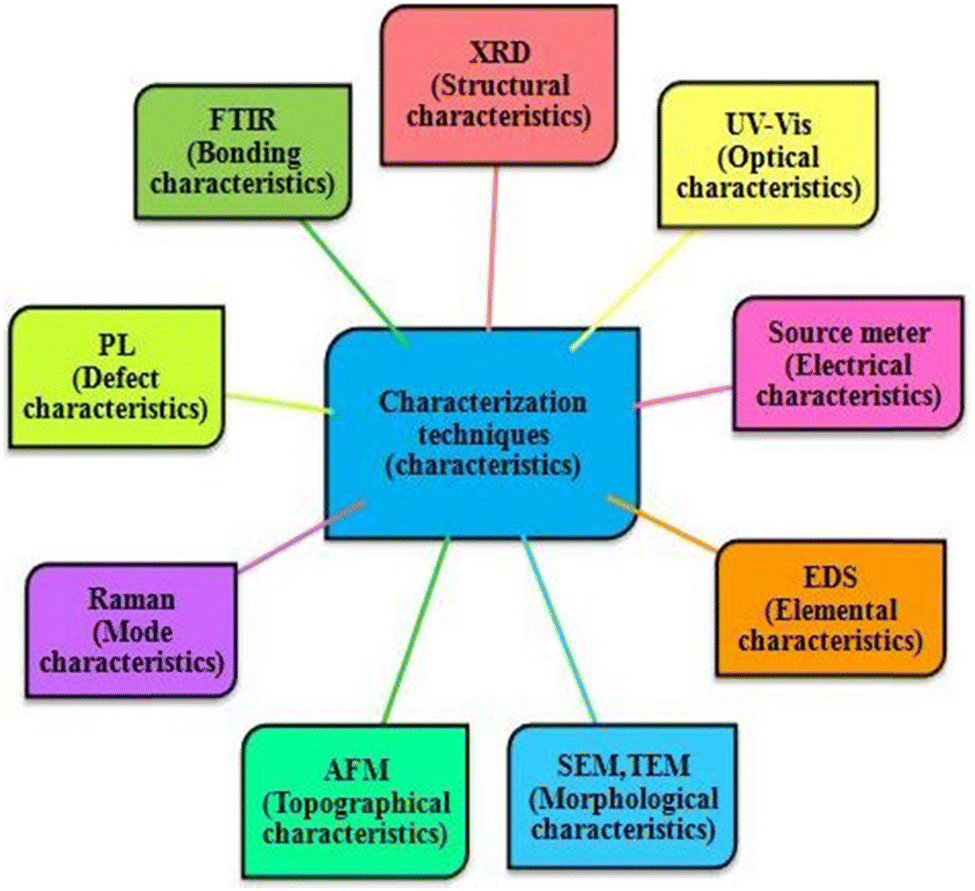
To address the issue of plateaued PCE of thin film solar cells (TFSCs), the development of novel, efficient and cheap multi-junction devices is necessary. Currently, a variety of absorber layer candidates are being investigated for tandem solar cell applications. Among them, cadmium zinc telluride (CdZnTe) is a II–VI compound semiconductor known for its outstanding characteristics to serve as the absorber layer in solar cells15–22 and physical properties of CdZnTe materials can be tuned or altered not only via heat and chloride treatment but also by varying the content of Zn. The performance of CdZnTe-based solar cells can be enhanced by addressing the transmission losses, thermalization and recombination losses, etc. and improving the physical properties of the CdZnTe absorber layers. Furthermore, CdZnTe material-based thin films are potential candidates for a wide variety of applications such as detectors,23–28 nano wires,29 substrates,30–34 and tandem solar cells,35–41 which can be applied as the top block, while Si-based, CIGS, organic or perovskite sub cells are potential bottom blocks for the development of multi-junction or tandem devices. Similar to CdZnTe, the band gap and associated properties of perovskite devices can be altered by varying the content of their constituents, and also be optimized to act as the bottom block in CdZnTe tandem devices. Thus far, significant efforts have been devoted to simulation modeling and device design employing CdZnTe materials for their application in specific technology.42–46 Consequently, frontier research has been undertaken employing CdZnTe thin films as the absorber layer in single-junction and multi-junction solar cells. Herein, a comprehensive review is presented on CdZnTe thin films together with their potential applications in the corresponding photovoltaic device technologies. Briefly, their associated properties, crystal structure, deposition techniques, device applications, effects of thermal annealing and chloride treatment (using CdCl2, MgCl2 and NH4Cl) and impact of elemental variation on the physical properties such as structural, optical, electrical, surface morphological, topographical and elemental characteristics and device fabrication are comprehensively discussed. Based on the literature to the date on CdZnTe thin films and their corresponding devices, the future perspectives and scope of these materials are presented in detail to maintain interest in them although they have a few drawbacks including a toxic constituent and achieving desirable performances comparable to that of the champion technologies dominating the market globally. Fig. 1 pictorially summarizes the various experimental tools used for the deposition and characterization of CdZnTe thin films, surface modifiers and the CdZnTe-based solar cell device architecture.
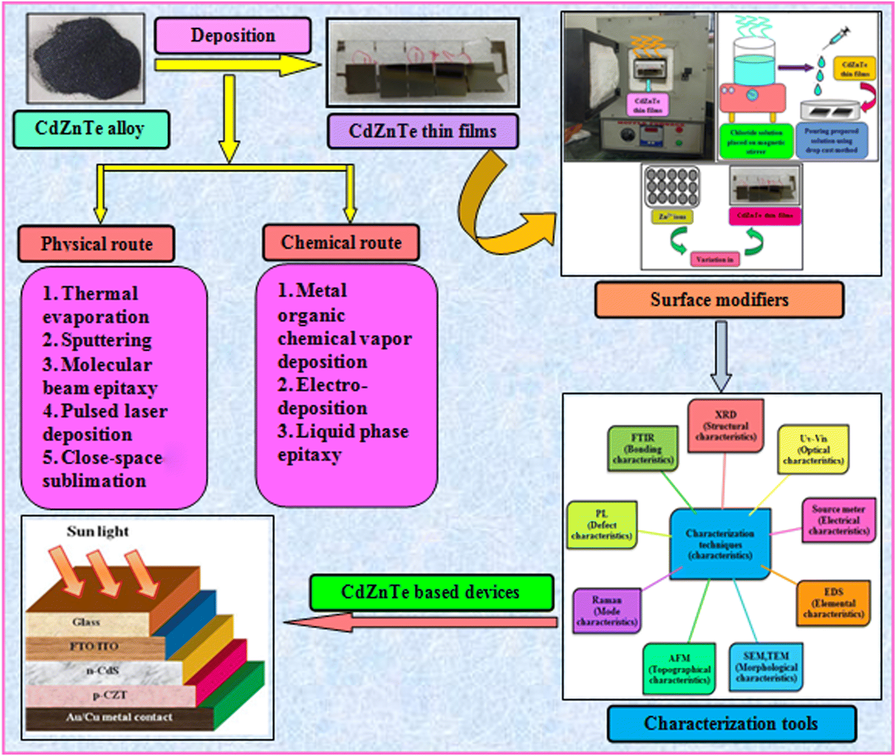 | ||
| Fig. 1 Pictorial illustration of the various experimental tools used for the deposition and characterization of CdZnTe thin films, surface modifiers and the CdZnTe-based solar cell device architecture. | ||
2. Crystal structure and properties of CdZnTe material
CdZnTe is a tertiary alloy composed of CdTe and ZnTe materials in the appropriate ratio depending on its application. CdZnTe has a cubic phase zinc blende crystal structure, which includes two merged face centered cubic (fcc) lattices. Fig. 2(a) presents the zinc blende atomic array of CdZnTe, where depending on its composition, the Cd or Zn atoms are located at the vertices and the face centers, whereas the Te atoms are situated at the four out of the eight tetrahedral corners. Hence, the CdZnTe lattice contains Cd2+ and Zn2+ cations and Te2− anions, where all the ions are arranged in a tetrahedral manner in the lattice and the four outer electrons are shared with the surrounding ones.47 Accordingly, the obtained iso-structural CdZnTe offers desirable properties such as band gap tunability, constituents with high atomic numbers, high absorption coefficient and carrier mobility, low leakage current, long-term stability, and diverse lattice parameters possibility,15–19 which are pictorially depicted in Fig. 2(b).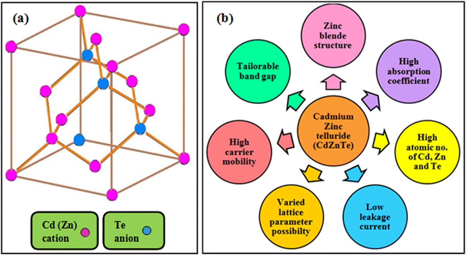 | ||
| Fig. 2 (a) Crystal structure and (b) properties of CdZnTe material. | ||
As stated, the CdZnTe material can be used in the form of thin films as the light-absorbing layer in single-junction and multi-junction solar cells, and therefore the next section is devoted to the deposition techniques used for the growth of CdZnTe absorber layers and their impact on the properties of these films in the corresponding applications.
3. Thin film deposition
Generally, a thin film is a thin layer of materials such as metals, insulators and semiconductors with a thickness ranging from a few nanometers to several micrometers on a substrate. Thin films can be developed for a wide range of applications and to realize the expectations of the corresponding architectures, their thickness can be varied and evolved. The properties of thin films are controlled by various pre- and post-treatments such as deposition methods and associated parameters, inclusion of dopant and additives, annealing temperature, duration, atmosphere, and grain boundary passivation treatment. The properties of thin films are different from their bulk counterparts, which can be attributed to their larger surface to volume ratio and smaller thickness. The deposition of a thin film involves applying a thin layer on a substrate, which can be solid, i.e., glass or metal supported, or flexible depending on the requirements. Presently, numerous advanced techniques are available for the deposition of thin films. These techniques are classified into two categories, namely, physical and chemical routes, which have certain merits and drawbacks. The selection of the deposition technique for the corresponding application depends on the properties of the materials employed such as purity, stability, melting point, and characteristics. Thus far, efforts have been devoted to the development of new recipes for film deposition to modify and improve the properties of CdZnTe thin films, reproduce the appropriate performance and cause the least deviation from the actual composition to develop high-performance devices.48–50Fig. 3 presents an overview of the thin film deposition methods.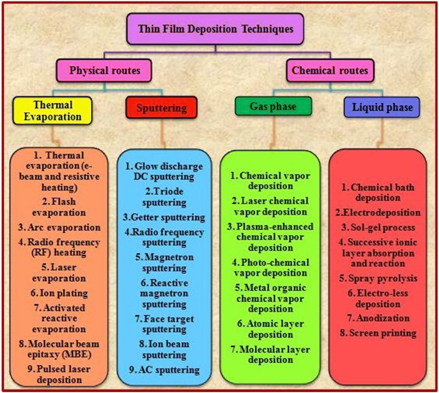 | ||
| Fig. 3 Overview of the various thin film deposition techniques.49 | ||
Considering the routes presented in Fig. 3, the physical route-based thermal evaporation-based resistive heating and sputtering techniques and chemical route-based gas phase and liquid phase recipes are briefly detailed in the following sub-sections together with the corresponding review of the target material.
3.1 Physical routes for the deposition of CdZnTe thin films
The physical route involves thermal evaporation and sputtering recipes, including evaporative and glow discharge processes. Typically, the physical route is also recognized as physical vapor deposition (PVD). In the evaporative process, vapors or evaporants are produced via a suitable process, and then allowed to adhere to the substrate, resulting in formation of a thin film. In the glow discharge process, a chemical reaction is initiated in the gas phase, which creates a glow discharge of the reactant gas, and consequently the source material is deposited on the substrate.48,51,52 In the physical route, various deposition techniques include electron-beam vacuum evaporation,53–59 resistive heating-based thermal evaporation,60–62 sputtering,63–69 molecular beam epitaxy (MBE),70,71 pulsed laser deposition (PLD)72,73 and close-space sublimation (CSS).74–79 The thermal evaporation technique is a vapor deposition technique following the physical route for the deposition of thin films. Based on the heating of the source material, this technique is further classified into two processes, namely, electron-beam vacuum evaporation and resistive heating thermal evaporation.51,52Employing the electron beam vacuum evaporation technique, Cd0.25Zn0.25Te thin films with varying thicknesses (500–2000 nm) were deposited on both glass and ITO substrates, where the ultra-vacuum of 5 × 10⁻⁶ Pa was maintained.53 Also, films having a thickness of 400 nm were developed on glass, ITO and silicon wafers under high vacuum of 1.5 × 10⁻⁶ torr54 and films with a thickness of 300 nm were deposited on ITO substrates under high vacuum (∼2 × 10⁻⁶ mbar), as measured by Penning and Pirani gauges.55 CdZnTe thin films were deposited on an Mo-coated glass substrate via the vacuum co-evaporation of CdTe and ZnTe powders, where the temperature of the CdTe and ZnTe evaporants was 893 K and 993 K, respectively, with a substrate temperature of 673 K.56 CdZnTe thin films were fabricated using the e-beam vacuum evaporation technique on glass and Si substrates, where the temperature of the substrate was maintained at room temperature and the pressure inside the vacuum chamber was kept at 2 × 10⁻⁴ Pa.57 Cd0.2Zn0.8Te thin films were prepared at room temperature using the e-beam technique onto glass substrate having a thickness of 1 μm.58 Cd0.2Zn0.8Te thin films were deposited by employing the e-beam vacuum evaporation technique at different substrate temperatures, i.e., 300 K, 373 K, 473 K and 573 K, and base pressure of 2 × 10⁻⁵ torr.59 Typically, the devices are fabricated by stacking metal contacts thus far using the resistive heating recipe, and thus in the following section, the resistive heating-based thermal evaporation recipe is discussed, which has also been employed thus far to develop CdZnTe thin film layers.
In this method, maintaining a high vacuum in the order of 10−5 to 10−6 mbar is essential to ensure the purity of the deposited films. To obtain deposited films with a uniform thickness, the substrate holder is rotated continuously a manner that each point on the target substrate surface receives the same amount of the vapor material. This technique is advantageous given that a wide variety of materials can be deposited using it.49 Cd1−xZnxTe thin films having varying Zn concentrations were deposited on glass and ITO substrates via thermal evaporation, where the working vacuum of ∼1.2 × 10⁻⁵ mbar was maintained by sustaining a base vacuum of ∼2.8 × 10⁻⁶ mbar.60 Cd1−xZnxTe thin films were developed for photovoltaic applications employing the resistive heating-based thermal evaporation technique, where the working vacuum of 1 × 10⁻⁵ mbar was maintained.61 The influence of the deposition technique on the physical properties of CdZnTe films was investigated, where CdZnTe layers were grown employing the electron beam and resistive heating techniques at a substrate temperature of 25 °C.62
Depending on the type of power supply used, the sputtering process is primarily classified into two categories, namely, direct current (DC) sputtering and radio frequency (RF) sputtering. Besides, the other prevalent sputtering processes are diode sputtering, bias sputtering, reactive sputtering, ion-beam sputtering and magnetron sputtering.51,52,80,83 Cd1−xZnxTe thin films were deposited on ITO substrates by repeated RF magnetron sputtering using a Cd0.9Zn0.1Te target at different substrate temperatures (200 °C, 300 °C and 400 °C), where the sputtering gas was set at a pressure of 5 Pa with a deposition time of 3 h.63 CZT thin films were fabricated on glass substrates employing DC magnetron sputtering at room temperature using a CZT target with a diameter of ∼2 inches and composition of 30 wt% Cd, 20 wt% Zn and 50 wt% Te, where the base pressure of ∼10−4 Pa was developed in the sputtering chamber.64 Cd1−xZnxTe multilayer films having a thickness in the range of 1360–9230 nm were deposited employing repeated RF magnetron sputtering on ITO-coated glass substrates using Cd0.9Zn0.1Te as the target material, where the substrate temperature was fixed at 300 °C with a sputtering power of 60 W.65 Aluminum (Al)-doped CdZnTe thin films were prepared using RF magnetron sputtering on ITO-coated glass substrates employing aluminum-induced crystallization (AIC) technology,66 where high-purity Al and Cd0.9Zn0.1Te crystal target were used. To implement AIC technology for the deposition of the CdZnTe/Al layer, the samples were heated for 60 min at 200 °C. Cd0.6Zn0.4Te thin films were deposited on FTO and cadmium sulphide (CdS) substrates employing RF magnetron sputtering.67 CdZnTe thin films of thickness 800 nm were grown on ITO substrates employing RF magnetron sputtering by fixing the sputtering power and pressure at 66 W and 1.5 Pa, respectively, where the applied target was developed by cutting a Cd0.9Zn0.1Te ingot.68 CdZnTe thin films were produced using RF magnetron sputtering on glass substrates at two substrate temperature of 200 °C and 400 °C by keeping the sputtering power at 80 W.69
3.2 Chemical routes to develop CdZnTe thin films
The chemical route based deposition processes are classified into two categories, namely, gas and liquid phases. In both processes, a chemical reaction takes place either in the gas-phase or liquid phase, which results in the deposition of the desired thin film on the corresponding substrates.51,86,87 The chemical process can also be further classified based on the type of precursor, applications, reactors used and chemical reactions.86 Among the chemical routes, techniques such as metal–organic chemical vapor deposition (MOCVD),88,89 electro-deposition/electro-plating90–92 and liquid-phase epitaxy93 have been frequently applied thus far to develop the CdZnTe thin films and the corresponding devices. These growth techniques are briefly discussed in the following sections together with a review of the corresponding target.| Technique(s) | Route(s) | Merits | Drawbacks | Ref. |
|---|---|---|---|---|
| Thermal evaporation (e-beam and resistive heating) | Physical | • Operation affability. | • Not suitable for fabricating multi-component thin films. | 82 |
| • Low cost. | • Varying evaporation rates and vapor pressures of different materials. | |||
| • Can be used with a wide variety of materials. | ||||
| Sputtering | Physical | • Provides deposited films with homogeneity. | • Requires appropriate control of the different deposition parameters. | 52 |
| • Constant sputtering rate for various materials. | ||||
| Molecular beam epitaxy (MBE) | Physical | • Capable of producing high-purity layered epitaxial thin films. | • Requires ultra-high vacuum for its operation. | 84 |
| • Slow deposition rates. | ||||
| Pulsed laser deposition (PLD) | Physical | • Effective for the development of epitaxial thin films and fabrication of multi-layered hetero-structures. | • Requires appropriate control of the different deposition parameters. | 84 |
| Close-space sublimation (CSS) | Physical | • Cost-effective. | • Requires appropriate control of the process parameters. | 85 |
| • High deposition rates | ||||
| Metal–organic chemical vapor deposition (MOCVD) | Chemical | • Used with a wide variety of substrates. | • Complexity of design and operation. | 95 |
| • Employed for both wide and narrow band gap semiconductors. | • Requires appropriate selection of the organo-metallic precursors. | |||
| Electro-deposition | Chemical | • Cost-effective. | • Operation does not require a vacuum system. | 97, 98 |
| • Easy manufacturing. | • Limited for the deposition of only metals. | |||
| • Appropriate for large-scale applications. | ||||
| Liquid phase epitaxy (LPE) | Chemical | • Provides a high growth rate. | • Only suitable for the growth of single-layered epitaxial films. | 95 |
| • Provides a wide selection of dopants. | • Solution removal is complex. | |||
| • Absence of any toxic by-products. |
Besides the deposition techniques, numerous post-treatments also affect the physical properties of CdZnTe thin films, which ultimately affect the target device performance. In the following section, we discuss the impact of surface modifiers, namely, thermal and chloride treatment and variation in Zn content on the physical characteristics of CdZnTe thin films.
4. Effect of thermal and chloride treatments and variation in Zn content on physical characteristics
The physical characteristics of CdZnTe thin films are affected by surface modifiers such as thermal and chloride treatment and variation in Zn composition, as described in Fig. 4(a)–(c), respectively. The surface of CdZnTe single crystals is comprised of defects such as Cd vacancies, Te interstitials, and dislocations.19,99 Hence, to minimize the presence of these defects and enhance the surface quality of CdZnTe thin films, surface modifiers are required. Firstly, thermal annealing or heat treatment at specific temperatures modifies the surface of CdZnTe thin films, and also reduces the number of surface defects.100 Secondly, polycrystalline thin films are comprised of grain boundaries, which act as trap states and recombination centers for charge carriers, and in the Cd-based layer, they be inverted by chloride activation, where the chlorine atoms are segregated in the grain boundaries, leading to their inversion or passivation. Therefore, the effect of chloride treatment has been widely studied by various researchers. Subjecting thin films to chloride treatment is an effective way to enhance their properties, given that it not only passivates the grain boundaries but also promotes grain growth, recrystallization, and the carrier lifetime and reduces the trap states and recombination centers.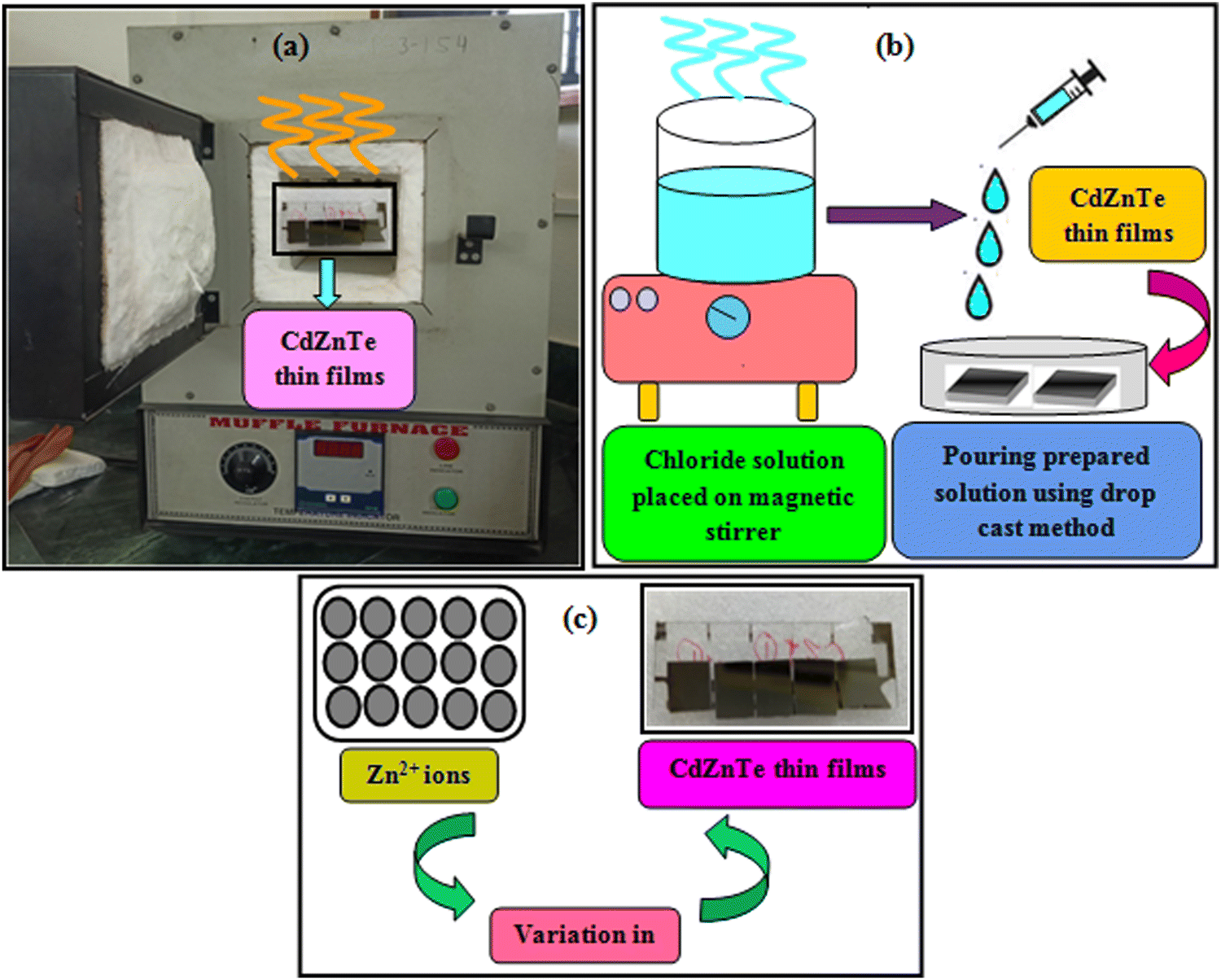 | ||
| Fig. 4 Pictorial illustration of (a) thermal annealing, (b) chloride activation treatment and (c) variation in Zn content on CdZnTe thin films. | ||
Chloride treatment is performed in two ways, namely, wet and dry chloride procedures. In ex situ wet chloride treatment, the samples are exposed to a CdCl2 solution having a specific concentration using the drop cast method, followed by annealing at suitable temperatures, and subsequent removal of the residual solution. In contrast, in in situ dry chloride treatment, a thin layer of CdCl2 is deposited in the same chamber on a previously deposited Cd-based layer, followed by annealing at suitable temperatures.67,101–103 Moreover, the Zn content chosen for the fabrication of ternary composites of Cd, Zn and Te also impacts the physical properties of CdZnTe thin films and needs to be further explored depending on the desired application.62,104
To optimize deposited films for desired applications or device development, their characterization is necessary, and therefore deposited thin films are usually studied using different characterization tools such as X-ray diffractometry (XRD), UV-Vis spectrophotometry, source meter (current measurements), scanning electron microscopy (SEM), atomic force microscopy (AFM) and energy dispersive spectroscopy (EDS) to optimize their structural, optical, electrical, morphological, topographical and elemental properties, respectively. A pictorial representation of the various characterization techniques is shown in Fig. 5. The performance parameters for solar cells such as short circuit current density, open circuit voltage, fill factor, and power conversion efficiency can be obtained by subjecting the prepared devices to supported electronics comprised solar simulator. Moreover, admittance parameters of developed CdZnTe solar cells can be determined by employing an LCR meter setup and the acquired short circuit current can be verified by performing quantum efficiency measurements. In the following sections, a comprehensive analysis is presented on the influence of surface modifiers on the structural, optical, electrical, topographical, and morphological properties of CdZnTe thin films for solar cell applications. In this section, the utilization of CdZnTe films is also highlighted as proficient absorber layers in the corresponding single-junction and tandem devices.
 | ||
| Fig. 5 Graphical representation of the various techniques for the characterization of thin films where UV-Vis stands for UV-Visible spectrophotometry and the tools are indicated by their prevelant abbreviations. | ||
4.1 Structural characteristics
X-ray diffraction (XRD) is recognized as the most powerful tool to probe the structure and phase of materials, where the diffracted beam is comprised of a large number of scattered rays mutually reinforcing each other. The XRD technique is based on Bragg's law of diffraction, which states that when an X-ray beam undergoes diffraction, it is scattered in all directions and the scattered rays are found to be in phase following the condition of constructive interference, and accordingly bright fringes appear.105–107 The assignment of the crystal structure, phase and Miller indices can be achieved by comparing the obtained crystallographic patterns with that of the Joint Committee on Powder Diffraction Standards (JCPDS) data. Based on the measurements, structural parameters such as crystallite size, crystallinity, lattice constant, lattice/inter-planar spacing, dislocation density, number of crystallites per unit area, texture coefficient, and stacking fault probability can be determined for a wide variety of materials and thin films.107–111The structural properties of Cd1−xZnxTe thin films were investigated using XRD,63 which showed that with an increase in the substrate temperature from 200 °C to 400 °C, the thin films possessed a polycrystalline structure with a (111) preferred orientation, the intensity and height of which increased with an increase in the substrate temperature. The associated full width at half maximum (FWHM) and dislocation density were found to decrease for the heated substrates, whereas the grain size increased, indicating the compact structure of the deposited films.63 The structural properties of as-deposited and 300 °C-annealed CdZnTe thin films were studied,64 where the as-grown films were amorphous in nature but the presence of humps in their diffraction patterns indicated that they tend to possess a zinc blende structure. Among the peaks, the peak corresponding to the (111) plane appeared to be dominant, while its intensity and the corresponding grain size increased and the FWHM decreased for the 300 °C-annealed CdZnTe thin films. The structural properties of Cd1−xZnxTe thin films deposited using the electro-deposition method were studied,92 where the films were grown using identical chemical baths at four different potentials, i.e., −550 mV, −650 mV, −750 mV and −850 mV, and annealed at 300 °C for 1 h. The XRD patterns confirmed the crystallization of the CdZnTe films along the cubic phase, where the presence of some other peaks in the XRD patterns was attributed to the substrate (SnO2) used for their deposition. Also, it was observed that an increase in the negative growth potential led to a decrease in the grain size of the CdZnTe films.
The impact of annealing on the structural parameters of e-beam-evaporated CdZnTe thin films was investigated,112 where the annealing temperature was varied in the range of 150–400 °C. The grain size was enhanced in the range of 26–72 nm upon heat treatment, indicating the improved crystallinity of the deposited films.112 The structural properties of CdZnTe thin films were also studied using one-step and two-step growth processes, where the substrate temperatures were varied in the range of 350–600 °C, and the results showed dominant diffraction peaks corresponding to the CZT (004) reflection, indicating the zinc blende structure of the films, and the other peaks corresponding to the CZT (002) reflection indicated the epitaxial growth of the deposited films.113 The XRD patterns of CdZnTe thin films under different mechanical polishing conditions and time114 revealed that all the CdZnTe thin films showed stronger diffraction peaks at around 2θ = 23.76°, corresponding to the preferential (111) orientation. The obtained (220), (311), (400) diffraction peaks were found to be very weak, indicating that the films preferentially grew along the (111) plane. The intensity of the diffraction peak corresponding to the (111) plane significantly increased with an increase in the polishing time. After polishing, the position of the (111) diffraction peak shifted slightly towards a smaller angle, which can be attributed to the influence of different Zn contents on the surface of CdZnTe. Also, with an increase in the mechanical polishing time and Zn content, the grain size was found to decrease.114
The XRD patterns of chemically prepared CdxZn1−xTe samples annealed at 300 °C using ammonia solution as the precipitating agent and NaBH4 solution as the reducing agent were recorded,115 and the patterns displayed three main diffraction peaks for CdxZn1−xTe at the 2θ values of approximately 24°, 39.44°, and 46.9°, which were identified corresponding to the (111), (220) and (311) planes of the cubic phase, respectively. In another work, the unit cell parameters were found to decrease from CdTe to ZnTe and the Cd0.8Zn0.2Te sample showed the lowest crystallite size of 22 nm with a higher micro strain and dislocation density. Also, with an increase in Zn content, the grain size improved from 22 nm to 71 nm.115 CdZnTe thin films having a thickness in the range of 450–1400 nm were deposited via the vacuum evaporation technique on unheated glass substrates using a multilayer method and the structural properties of both the as-deposited and heat-treated samples were investigated at different CdTe source temperatures.116 As observed, the preparation conditions and Zn content in the CdTe/Zn samples played a significant role in the modification of their structural characteristics. During heat treatment of the Zn sub-layers between the CdTe layers, Zn diffusion in the CdTe adjacent layers resulted in an improvement in the crystallinity of the films via the inclusion of Zn atoms in the CdTe lattice. The effect of varying annealing conditions (air, CdCl2 and MgCl2 treatment) on the structural properties of thermally evaporated CdZnTe thin films was reported,117 where the dominant (111) plane was observed for all the films and their grain size was enhanced, whereas the amount of defects was reduced for the air-annealed and chloride-treated films. Several other reports67,118 also revealed that chloride activation treatment led to an enhanced dominant peak intensity and crystallinity in CdZnTe thin films, indicating the crucial impact of chloride treatment on improving the film quality.
CdxZn1−xTe films having varying Zn concentrations (x = 0.0–1.0) were deposited via the vacuum co-evaporation method,119 where the X-ray diffractograms of the films (in normal and enlarged views) are shown in Fig. 6(a) and (b), respectively, which revealed the (111) dominant orientation for all the films. Also, the intensity of the dominant peak and other structural parameters such as the grain size, dislocation density and micro-strain varied with a change in the Zn concentration.
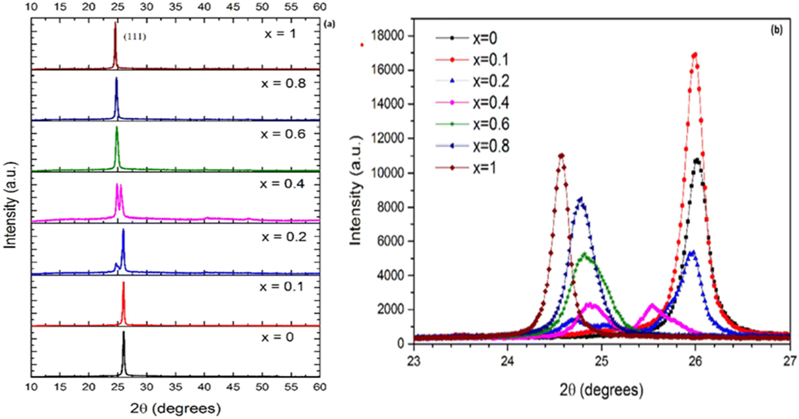 | ||
| Fig. 6 (a) XRD patterns of Cd1−xZnxTe thin films at varying Zn concentrations and (b) enlarged portion of the diffractograms in 2θ range of 23–27°, showing the position of the dominant peak. Reproduced from ref. 119 with permission, Copyright (2020), Elsevier Ltd. | ||
The effect of various surface modifiers on crystallite size calculated using XRD for physically and chemically deposited CdZnTe films is shown in Table 3.
| Surface modifier(s) | Deposition technique(s) | Crystallite size (D) nm | Ref. |
|---|---|---|---|
| Annealing | Sputtering | 38–81 | 63 |
| Annealing | Electron beam evaporation | 26–72 | 112 |
| Zn content variation | Close-space sublimation | 34–45 | 114 |
| Zn content variation | Chemical bath deposition | 22–72 | 115 |
| Annealing | Electron beam evaporation | 29–41 | 117 |
| Chloride treatment (CdCl2) | Electron beam evaporation | 29–44 | 117 |
| Chloride treatment (MgCl2) | Electron beam evaporation | 29–42 | 117 |
| Zn content variation | Vacuum co-evaporation | 18–42 | 119 |
Due to the instrumentation resolution limit, the crystallite/grain size of more than 50 nm acquired using the XRD technique should be verified via transmission electron microscopy (TEM) measurements. The structural parameters such as crystallinity and grain/crystallite size for the constituent absorber layers in thin film solar cells should be higher and the grain boundary (GB) density should as low as possible. The other structural parameters such as inter planar spacing, lattice constant, internal strain, dislocation density and number of crystallites per unit area are typically found to be consistent with the grain size and position of the dominant peak. There is a stronger correlation between the structural properties and other physical properties such as optical, electrical, surface morphological and topographical properties. Therefore, the aim is to achieve the largest possible grain growth for the single constituent layer, followed by its implication in the corresponding device to enhance the performance of developed solar cell devices.
4.2 Optical characteristics
The investigation of the optical properties and parameters such as optical energy band gap, spectral behavior of the refractive index, lattice dielectric constant, dispersion energy, single oscillator energy, Urbach energy, absorption coefficient, extinction coefficient, surface energy loss function (SELF), and volume energy loss function (VELF) of materials can be typically carried out employing UV-Vis spectroscopy by measuring absorbance, transmittance and reflectance spectra in the near-ultraviolet (190–380 nm) and visible (380–780 nm) range, where the associated instrumentation wavelength range is from the minimum of 190 nm to the maximum of 1100 nm. UV-Vis NIR spectrophotometers are used to measure spectra in the wavelength range of 190–3300 nm. The typical manufacturing and associated instrumentation are based on solar irradiance, which is dominated by the visible range not only at the earth but also near the sun. This radiation provides sufficient energy for electronic transitions, and consequently the optical spectrum of the sample under observation is obtained. The amount of radiation absorbed by the sample is related to its concentration and path length and is governed by Beer–Lambert's law, which states that the absorbance of a sample is directly proportional to its concentration and path length of the associated sample holder.120,121 The optical energy band gap can be estimated using different approaches such as Tauc plots, derivative transmittance spectroscopy, and diffuse reflectance spectroscopy. The spectral behavior of the refractive index can be determined using the Swanepoel envelope method. Different dispersion parameters of materials and thin films can be obtained using the Wemple-Di Domenico (WDD) model. Thus, by using UV-Vis spectroscopy, a comprehensive analysis of the optical parameters considering the associated applications can be performed.122–125Numerous researchers have investigated the influence of different modifiers on the optical properties of CdZnTe thin films, with the aim to align and optimize their properties considering their utilization in single- and multi-junction solar cells. The optical characteristics of sputtered Cd1−xZnxTe thin films were analyzed as a function of the substrate temperature (200–400 °C) and the transmittance of the films attained was in the range of 5–20%, where the films exhibited a lower transmittance and higher absorbance. Also, with an increase in the substrate temperature, the optical energy band gap decreased in the range of 1.514–1.507 eV due to the increment in the grain size and decrease in the amount of defects.63 The optical properties of Cd1−xZnxTe thin films deposited using the electro-deposition technique were analyzed92 and it was observed that the transmission spectra of the films grown at −800 mV and −850 mV showed a step-like nature in the region where absorption occurred for both samples. This step-like nature indicated nanocrystalline behavior, resulting from the discrete nature of the energy levels and step-like density of states. Also, it was observed that with an increase in the Zn content from 0 to 0.4, the optical energy band gap varied in the range of 1.55–1.8 eV.92 Similar results were reported by Chander et al.,112 where the energy band gap decreased upon heat treatment for e-beam-evaporated CdZnTe thin films.
The Tauc plots of chemical bath-deposited CdxZn1−xTe films with varying Zn contents of 0.0, 0.2, 0.5, 0.8 and 1.0 were reported,115 where their Eg was found to be 1.37 eV, 1.5 eV, 1.65 eV, 1.8 eV and 2.1 eV, respectively. The reported work showed that the addition of Cd to substitute Zn metal led to a decrease in Eg or an increase in Zn content led to an increase in band gap. The effect of different annealing conditions, i.e., air annealing and CdCl2 and MgCl2 treatments, on the optical properties of e-beam-evaporated CdZnTe thin films was investigated,117 where in the case of the pristine films, Eg = 1.55 eV was attained. In the case of the air-annealed, CdCl2- and MgCl2-treated films, the optical energy band gap decreased not only for the air-annealed films but also for the chloride-treated films, which was in the range of 1.44–1.54 eV, 1.43–1.53 eV and 1.41–1.52 eV, respectively.
The impact of chloride activation treatment on the optical properties of sputtered CdZnTe thin films was studied118 and chloride activation corresponding to different atmospheres of hydrogen, nitrogen and dry air led to a decreased Eg from 1.82 eV to 1.61 eV. The optical characteristics of CdxZn1−xTe thin films having a low Zn concentration (x = 0.0–1.0) deposited using the vacuum co-evaporation method were reported,119 where their transmittance spectra revealed the presence of an absorption edge corresponding to the wavelength range of 500–820 nm. Also, the optical energy band gap decreased with an increase in Zn content and determined to be in the range of 1.53–2.17 eV. Fig. 7(a) and (b) show the Tauc plots and achieved optical energy band gap as a function of Zn content for Cd1−xZnxTe thin films for reference to understand this empirical recipe graphically.
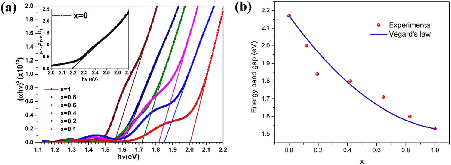 | ||
| Fig. 7 (a) Tauc plots where vertical scale bears unit (cm−1 eV)2 and (b) variation in optical energy band gap as a function of Zn content for Cd1−xZnxTe thin films. Reprinted from ref. 119 with permission, Copyright (2020), Elsevier Ltd. | ||
The optical properties of vacuum-annealed Cd1−xZnxTe thin films were reported,126 where the films were deposited via the vacuum evaporation method. The films were annealed in the temperature range of 300–450 °C and their energy band gap was determined to be in the range of 1.38–2 eV. The reduced energy band gap for the 325 °C- and 400 °C-vacuum annealed films may be due to the presence of defects and impurities in the films. Hence, the optical parameters of CdZnTe thin films are significantly altered by various treatments. The evolution of the optical energy band gap with different surface modifiers estimated using Tauc plots for films deposited employing various physical and chemical deposition techniques is presented in Table 4.
| Surface modifier(s) | Deposition technique(s) | Optical energy band gap (Eg) eV | Ref. |
|---|---|---|---|
| Annealing | Sputtering | 1.507–1.514 | 63 |
| Zn content variation | Electro-deposition | 1.55–1.8 | 92 |
| Annealing | Electron beam evaporation | 1.76–2.17 | 112 |
| Zn content variation | Chemical bath deposition | 1.37–2.1 | 115 |
| Annealing | Electron beam evaporation | 1.44–1.55 | 117 |
| Chloride treatment (CdCl2) | Electron beam evaporation | 1.43–1.55 | 117 |
| Chloride treatment (MgCl2) | Electron beam evaporation | 1.41–1.55 | 117 |
| Chloride treatment (CdCl2) | Sputtering | 1.61–1.82 | 118 |
| Annealing | Physical vapor deposition | 1.38–2.0 | 126 |
The absorber layer in solar cells should have a high absorption coefficient and low transmittance in the visible region. As stated, CdZnTe thin films are used as the absorber layer in solar cell devices, and thus attempts have been made to optimize their optical energy band gap around the optimal energy band gap, which is about 1.4 eV for single-junction devices considering the solar irradiance available on the Earth's surface and the Shockley–Queisser limit based on the principle of detailed balance.
To apply these absorbers in tandem devices as the top block, the Eg should be optimized in the range of 1.5–2.0 eV for the corresponding sub cell to harvest the maximum incident spectra, where low optical energy band gap absorber layer based sub-cells such as Si-based, organic and perovskite solar cells can be applied as the bottom block by optimizing their Eg in the range of 1.0–1.4 eV depending on the device architecture.
4.3 Electrical characteristics
The electrical properties of films such as current and voltage behavior, resistivity, conductivity, carrier concentration, and mobility can be investigated using a source meter/electrometer112 and Hall measurement system.127 Generally, a source meter/electrometer is a device used to measure the electrical properties of materials and thin films precisely, which measures the current flow or potential difference of charges. By coupling a source meter with a solar simulator, it can also be employed to determine the electrical properties and performance parameters of solar cell devices. A source meter has merits compared to the common current–voltage measuring devices, including it can perform both voltage and current measurements simultaneously in the forward and reverse directions, covers a wide operating range, high resolution, user friendly interface owing to numerous applications in batteries, solar cells and other devices and allows measurement of basic physical quantities at faster rates with high accuracy and sensitivity. Thus, it is used to perform current voltage measurements to determine the electrical properties of thin films and performance of devices.The dark current–voltage (I–V) characteristics of Au/CdZnTe/ITO and Au/CdZnTe/Au sandwich-structures were determined as a function of Zn concentration, where non-linear and linear behaviors were observed, respectively, and the resistivity of the films increased with an increase in Zn concentration due to the widened optical energy band gap.20 The photo-induced electric bi-stability properties of sputter-deposited pristine and 300 °C-annealed CdZnTe thin films under light and dark conditions were analyzed, where the I–V curves indicated high conductivity under illumination, i.e., the electrical bi-stability was enhanced under light conditions for both samples. Under dark conditions, the films revealed no electric bi-stability and the conductivity of the 300 °C-annealed CdZnTe thin films was found to be much higher than that of the pristine films.64 The current–voltage characteristics of CSS-deposited Au and Au/ZnTe:Cu electrodes on pristine and polished CdZnTe thin films were investigated77 and found to be non-linear (non-Ohmic) and linear (Ohmic), respectively. The electrical properties of vacuum-evaporated CdZnTe thin films were reported,112 where their I–V characteristics indicated linear current behavior with voltage. The electrical conductivity was found to increase with annealing owing to the increase in grain size or grain growth due to the recrystallization of the grains and decrease in grain boundaries. The electrical properties of CdZnTe thin films prepared under different annealing conditions (air, CdCl2 and MgCl2) were studied, where in the case of the air-annealed and CdCl2-treated films, their conductivity decreased, whereas that of the MgCl2-treated films varied with the treatment temperature.117 Moger et al.119 studied the electrical properties of vacuum co-evaporated CdxZn1−xTe thin films as a function of Zn concentration (x = 0.0–1.0) and observed that the electrical resistivity varied with the Zn content. The samples with x = 0.0 and x = 1.0 concentration (ZnTe) exhibited p-type and n-type conductivities, respectively. The resistivity measurements were performed employing the van der Pauw method and the results revealed that the chosen Zn content had a significant impact not only on the carrier type and mobility but also on the resistivity of the thin films. The electrical properties of Cd1−xZnxTe thin films were investigated via Hall effect and resistivity measurements,128 where the positive sign of the Hall coefficient (RH) confirmed the p-type semiconducting nature of all the Cd1−xZnxTe thin films. The resistivity of the films varied, which increased initially, attained the maximum value at a Zn composition of x = 0.2, decreased to the minimum value at x = 0.8, and then slightly increased again at x = 1.0. The carrier concentration also varied, i.e., initially increased with an increase in x up to 0.4, and then slightly decreased at x = 0.6. The maximum carrier concentration was observed at x = 0.8, and later found to decrease at x = 1.0. The maximum and minimum mobilities were found to be about 11.54 cm2 V−1 s−1 and 0.17 cm2 V−1 s−1 for the films having x = 0.6 and x = 0.2 concentrations, respectively.
The effect of surface modifiers on the electrical resistivity of CdZnTe thin films deposited via various physical and chemical deposition routes is presented in Table 5.
| Surface modifier(s) | Deposition technique(s) | Resistivity (ρ) Ω cm | Ref. |
|---|---|---|---|
| Zn content variation | Close-space sublimation | 2 × 10⁸–6.5 × 10⁹ | 20 |
| Annealing | Electron beam evaporation | 0.64–2.68 × 10² | 117 |
| Chloride treatment (CdCl2) | Electron beam evaporation | 0.64–2.56 × 10² | 117 |
| Chloride treatment (MgCl2) | Electron beam evaporation | 0.53–2.01 × 10² | 117 |
| Zn content variation | Vacuum co-evaporation | 2.84–5.36 × 10³ | 119 |
| Zn content variation | Close-space sublimation | 1.73 × 10³–1.28 × 10⁵ | 128 |
To develop high-efficiency solar cell devices, the current–voltage (I–V) characteristics of CdZnTe thin films should be linear or films should possess Ohmic character and the electrical parameters such as carrier concentration, mobility and conductivity of the absorber films should be high, while their electrical resistivity should be as low as possible.
4.4 Morphological characteristics
The surface morphological features such as shape, size and orientation of the grains play a vital role in modification of the quality of films and performance of the corresponding devices. The visualization of the grain boundaries and defects such as cracks, pinholes, and voids can be explicitly done using different microscopy techniques. The surface morphological and micro-structural characteristics of nano-materials and thin films can be observed employing scanning electron microscopy (SEM) and transmission electron microscopy (TEM), which are described herein in detail in the context of CdZnTe thin films with the appropriate scientific interpretation.The impact of different surface modifiers on the morphological properties of CdZnTe thin films has been widely investigated by various research groups employing SEM. The SEM micrographs of sputtered CZT films deposited at different substrate temperatures (200–400 °C) were recorded,63 where their morphology was enhanced with an improved grain size or grain growth and decreased grain boundaries with an increase in the substrate temperature. The results showed that the substrate temperature had an explicit impact on the crystallization quality, which may help to reduce the trapping effects among grain boundaries by improving the charge carrier collection.63
The surface morphological properties of PLD-deposited CdxZn1−xTe thin films from two targets (hot-pressed and annealed) over several compositions (x = 0.00, 0.03, 0.06, 0.10, 0.20, and 1.00) were investigated, where all the films were found to be uniform, having the same thickness and crystal size. Also, a low temperature reduced the grain growth, while regardless of the target type, as the Zn concentration increased, the porosity decreased.72 The surface morphology of CdZnTe thin films with an increase in the substrate temperature and growth time, namely, A1 (substrate temperature of 350 °C and growth time of 27 s), A2 (substrate temperature of 430 °C and growth time of 53 s), B1 and B2 (substrate temperature of 350 °C and growth time of 230 s) is shown in Fig. 8(a)–(d) for the clarity and understanding the grain growth mechanism. The surface morphology of the A1 film (Fig. 8(a)) revealed surface coverage with a layer of continuous and homogeneous islands, indicating that the nucleation process was faster and lesser sensitive to the surface asymmetry of GaAs. The islands in the A2, B1 and B2 films (Fig. 8(b)–(d), respectively) were larger in size or had larger grain growth compared to the A1 film, which was less compact even with a longer growth time. The size of the islands in the CdZnTe films estimated from the SEM images was in the range of 30–300 nm, which was much larger than that of the crystallite/grain size, as calculated employing XRD measurements.76
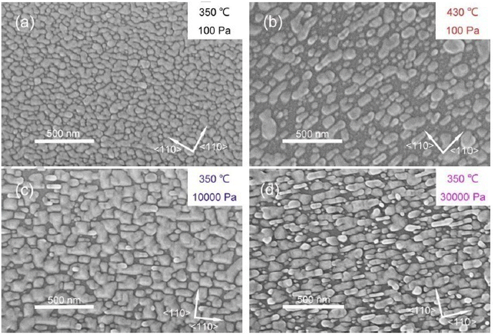 | ||
| Fig. 8 Surface morphological images of (a) A1, (b) A2, (c) B1 and (d) B2 CdZnTe samples. Adapted with permission from ref. 76 Copyright (2018), Elsevier Ltd. | ||
SEM micrographs of CSS-deposited CdZnTe thin films over different substrate temperatures (100–500 °C) were recorded,79 which revealed that as the substrate temperature increased, some voids and pitfalls appeared in the surface morphology of all the films. Also, the grain size increased with an increase in the substrate temperature up to 400 °C, and thereafter decreased. The field-emission scanning electron microscopy (FE-SEM) images of 300 °C-annealed CdxZn1−xTe samples (x = 0.0, 0.2, 0.5, 0.8 and 1.0) synthesized via the wet chemical method were studied,115 which showed cloud-like structures in the Cd0.2Zn0.8Te thin films. The Cd0.5Zn0.5Te thin films had dense network-like structures and the Cd0.8Zn0.2Te films showed a prismatic-like morphology with better crystallinity than the other films. The impact of cadmium chloride activation on the morphological properties of CdZnTe thin films was investigated,118 where in the case of the as-grown films, they possessed a spherical uniform morphology. For the samples thermally treated at 380 °C and 400 °C, spherical large-sized grains were observed owing to the coalescence and recrystallization of the grains upon chloride treatment. The morphological micrographs of vacuum co-evaporated CdxZn1−xTe thin films were studied as a function of Zn content (x = 0.0–1.0), where the SEM images revealed a spherical homogenous and crack-free morphology for all the films.119
The surface morphological properties of CSS-deposited CdxZn1−xTe thin films with varying Zn contents were reported, where an increase in the Zn concentration from 0.0 to 1.0 resulted in a decrease in the grain size from 9 μm to 1.8 μm.128
The effect of surface modifiers on the grain size estimated employing SEM for films deposited via different physical and chemical deposition techniques is shown in Table 6.
| Surface modifier(s) | Deposition technique(s) | Grain size (D) | Ref. |
|---|---|---|---|
| Zn content variation | Pulsed laser deposition | 20 nm | 72 |
| Annealing | Close-space sublimation | 30–300 nm | 76 |
| Annealing | Close-space sublimation | 0.4–1 μm | 79 |
| Zn content variation | Chemical bath deposition | 1–2.5 μm | 115 |
| Zn content variation | Close-space sublimation | 1.8–9 μm | 128 |
The surface morphology of CdZnTe thin films should be compact and homogenous without any crystallographic defects such as pinholes and voids and the grain size of the corresponding absorber or constituent layers should be higher to achieve devices with better performances. As stated, TEM also gives information about the surface morphology, grain growth and microstructure of the constituent thin film layers, and therefore the next sub-section includes an overview of TEM with a detailed analysis.
To perform an in-depth micro-structural analysis of CdZnTe thin films, researchers have analyzed the impact of surface modifiers using TEM. TEM and HRTEM micrographs of annealed and pristine samples of Cd1−xZnxTe thin films were captured88 and the results showed that the thickness and grain size of these films were of the same order of ∼5 μm and multiple twinning was observed. Also, no transitional layer was observed between the films and bottom glass substrate. At a temperature of up to 300 °C, the grain size did not change significantly in the films; however, twins and stacking faults were observed on the sample surface. The HRTEM micrographs revealed the presence of dislocations near the grain boundaries, which formed glide bands inside the grains. For reference and understanding, the TEM micrographs of Cd1−xZnxTe thin films deposited using the MOCVD method are depicted in Fig. 9, where the effect of annealing on these films was studied at 200 °C and 300 °C. In these films, their surface was modified by four processes, as follows: (a) recrystallization started at 200 °C, increasing the grain size, and at 300 °C, the grain size increased from 0.1 μm to 1.5 μm; (b) the mechanical twinning process produced thin-lamella-like structures on the surface of the films; (c) spinodal decomposition started at temperatures > 250–300 °C, where TEM selected area diffraction (SAD) indicated broadening of the diffraction rings owing to the phase transformation; and (d) ordering process, in which the ordered areas showed strong absorption and referred to as “black clouds” in the TEM micrographs. Thus, thermal annealing below 300 °C modified the surface of the films by these four processes, i.e., recrystallization, twinning, decomposition and ordering.89
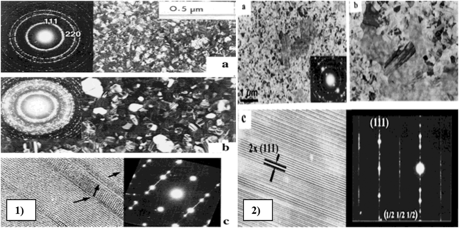 | ||
| Fig. 9 TEM images of (1) Cd0.48Zn0.52Te thin films: (a) as-deposited state, (b) after in situ annealing for 15 min at 250 °C, and (c) HRTEM images. (2) In situ Cd0.48Zn0.52Te thin films annealed at 250 °C for (a) 30 min and (b) 33 min and (c) HRTEM images. Reproduced from ref. 89 with permission, Copyright (2002), Wiley-VCH. | ||
The TEM images of CdCl2-treated Cd0.6Zn0.4Te thin films were analyzed,132 where the effect of chloride treatment on the sample surface was found to be prominent given that obvious recrystallization and grain growth started at the surface and proceeded towards the CdS/CdZnTe junction. Initially, the surface consisted of columnar-shaped grains having a high density of stacking faults below the recrystallized region, whereas after recrystallization, the morphology changed to oval-shaped. The effect of the metal-semiconductor interface of gold contacts on 85 °C-baked CdZnTe thin films was investigated employing the electro-less deposition method,133 where the TEM micrographs of these films revealed the presence of bright grains deep in the subsurface, which were dispersed throughout the surface, indicating their uniform deposition.
In the case of CdZnTe thin films, TEM analysis provides information not only about the grain size of the deposited films but also visualizes processes such as recrystallization, mechanical twinning, decomposition and spontaneous ordering in thin films. These processes offer evidence about significant changes associated with the morphology, phase transformation and defects present on the surface of the thin film.
In the present section, the surface morphological properties of CdZnTe thin films are described carefully together with their implication in order to enhance performance of the corresponding devices. Besides morphology, the surface topography of each layer also influences the properties and performance of the devices because a higher surface roughness is required for the absorber layer to enhance the absorption probability of incident photons through multiple scattering based on the principle of total internal reflection. Therefore, in the next section, an overview of the surface topography of the target domain is presented, which is typically observed employing atomic force microscopy (AFM).
4.5 Topographical characteristics
AFM is a particular type of scanning probe microscopy (SPM), which is based on the piezoelectric effect and uses the inter-atomic forces between the tip and specimen for the topographical characterization of the surface of the sample under investigation. AFM produces both two-dimensional (2D) and three-dimensional (3D) images of the specimen and can be used with non-conducting specimens, where 2D images are real, while the 3D images are artifacts.134,135 The basic set-up of a typical AFM includes a specimen holder, spring cantilever, laser and detector. The specimen holder holds the specimen (sample) under observation, the spring cantilever is used together with an integrated tip at one end, the laser beam measures the inter-atomic forces between the tip and specimen and the detectors process the collected information related to the specimen surface. Upon rastering the cantilever tip over the specimen surface, an inter-atomic potential is developed between the tip and sample surface, and consequently the cantilever moves upwards and downwards and these deflections are measured by the detector, producing 2D, and then 3D images of the specimen.134–136 The measurements of topographical characteristics using AFM can be performed in three modes, i.e., contact, non-contact and semi contact or intermediate mode.The effect of thermal treatment on the topographical properties of vacuum-evaporated Cd0.2Zn0.8Te thin films was investigated,58 where homogeneously distributed grains were attained and the RMS roughness of the annealed Cd0.2Zn0.8Te thin films was determined to be 6 nm. Prabakar et al.59 explored the impact of substrate temperature (300 °C) on the 2D AFM images of Cd0.2Zn0.8Te thin films, where the films had a spherical-shaped granular morphology/topography and their RMS roughness changed with the substrate temperature. The effect of different Zn contents (x = 0.05–0.15) on the topographical properties of 300 °C-annealed CdxZn1−xTe thin films was analyzed,60 where the films were deposited via the resistive heating-based thermal evaporation technique. All the films revealed a hill-like topography comprised of small-large height hills and the root mean square (RMS) roughness varied in the range of 7–16 nm with a variation in the Zn concentration. The AFM images of RF-sputtered CZT thin films deposited at varying substrate temperatures of 200 °C, 300 °C and 400 °C were analyzed, which showed that the films deposited at 200 °C had pebble-like crystal grains with a size of 130 nm. The CZT films deposited at 300 °C exhibited a complete grain shape with a size of 253 nm and better degree of crystallinity, whereas the films deposited at 400 °C demonstrated a denser structure with a grain size of 300 nm. As the substrate temperature increased, the grain size increased, which may be due to the kinetic limitation at low temperature.63 The topographical properties of RF-sputtered CdZnTe thin films were observed,68 where the substrate temperature was set at 300 °C and pebble-like structures were formed, having a mean diameter of 143 nm. Cao et al.113 studied the topographical images of CSS-deposited CdZnTe thin films corresponding to the first-step and second-step growth temperatures in the range of 350–600 °C, as shown in Fig. 10(a)–(d), where ridge-like topographies were acquired for all the films and their RMS roughness was in the range of 0.33–1.23 nm. The 3D topographical images of vacuum co-evaporated CdxZn1−xTe thin films were studied as a function of Zn content (x = 0.0, 0.4 and 1.0) and the AFM images revealed a medium to large height hill-like topography. Also, the RMS surface roughness varied from 4.01 nm to 5.66 nm with an increase in the zinc content.119
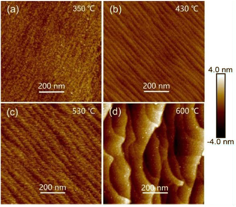 | ||
| Fig. 10 2D AFM images of CdZnTe thin films deposited at one-step growth temperature of 350 °C and second-step growth temperatures of (a) 350 °C, (b) 430 °C, (c) 530 °C, and (d) 600 °C. Reprinted from ref. 113 with permission, Copyright (2019), Elsevier Ltd. | ||
The effect of surface modifiers on the topographical features such as surface roughness and mean grain size calculated using AFM for CdZnTe thin films deposited via various physical and chemical deposition techniques is presented in Table 7.
| Surface modifier(s) | Deposition technique(s) | RMS roughness (nm) | Mean grain size (nm) | Ref. |
|---|---|---|---|---|
| Annealing | Vacuum evaporation | 6 | — | 58 |
| Annealing | Vacuum evaporation | 3.2–5.8 | — | 59 |
| Zn content variation | Resistive heating thermal evaporation | 7–16 | — | 60 |
| Annealing | Sputtering | — | 130–300 | 63 |
| Annealing | Sputtering | — | 143 | 68 |
| Annealing | Close-space sublimation | 0.33–1.23 | — | 113 |
| Zn content variation | Vacuum co-evaporation | 4.01–5.66 | — | 119 |
To prepare high-quality CdZnTe thin films, their grain size should be high, while AFM findings should be correlated with the SEM and XRD findings, and if any deviation is observed, appropriate scientific interpretation of the facts is necessary to mitigate the problem in the future. The surface roughness of the corresponding absorber layer should be high given that it enhances the chances of absorbing of incident photons by the phenomenon of multiple scattering or total internal reflection as stated earlier.
4.6 Elemental characteristics
The compositional analysis of thin films and materials can be undertaken via energy dispersive spectroscopy (EDS)/energy dispersive X-ray spectroscopy (EDAX), which is based on the fundamental principle of the spectroscopy, i.e., each atom has a unique atomic structure, and consequently produces characteristic X-rays, appearing as a unique set of peaks. A typical EDS consists of four main components, i.e., an excitation source, X-ray detector, pulse processor and analyzer. An e-beam or X-rays can be used as the excitation source, the X-ray detector is used to collect information, the pulse processor is utilized for processing the collected information and the analysis is accomplished by an analyzer.137–139EDS has been widely employed by the scientific community to investigate the composition and confirm the stoichiometry to implicate the optimized films in the targeted domain. For readers to understand EDS, a the elemental analysis of annealed CdZnTe thin films is shown in Fig. 11(a)–(c), where Cd, Zn and Te peaks confirmed the successful deposition. Besides these peaks, oxygen (O) and silicon (Si) peaks are also present in the spectra due to the indium-doped tin oxide (ITO)-coated glass substrate underneath the deposited CdZnTe thin films. The Cd and Zn concentrations increased, whereas the Te concentration decreased upon annealing, indicating a shift in the preferred diffraction peak towards a higher side.55 These alterations in the peaks can be supported and correlated by other physical characteristic findings depending on the aim of the researcher.
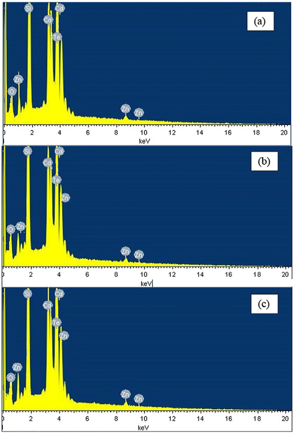 | ||
| Fig. 11 EDS spectra of CdZnTe thin films thermally annealed at (a) 100 °C, (b) 200 °C, and (c) 300 °C. Adapted from ref. 55 with permission. Copyright (2017), Elsevier Ltd. | ||
The EDS spectra of CZT films deposited at different substrate temperatures were studied, where a decrease, increase and no variation were observed for the applied concentrations of Zn, Cd and Te, respectively. The lower Cd content than Zn content may be due to the loss of Cd during deposition and its associated low sticking coefficient.63 The elemental properties of sputtered CZT thin films were studied, where their EDAX spectra confirmed the deposition of the pristine and 300 °C-annealed films, and the chemical composition was found to be 13.39%, 27.87% and 58.74% and 12.95%, 28.14% and 58.91% for Cd, Zn and Te elements, respectively.64 To introduce suitable grain growth, CdCl2-treated RF-sputtered Cd0.6Zn0.4Te films were explored, where their EDAX spectra confirmed the deposition, and a considerable loss was observed in Zn content given that the CdCl2 vapors reacted with Zn, resulting in the formation of ZnCl2.67 The elemental analysis of Cd1−xZnxTe thin films synthesized via the electro-deposition method92 revealed the dependence of the Zn content on the ionic composition of the starting solution, where the Zn/Cd ratio in the films increased consistently with an increase in the ionic Zn/Cd ratio in the chemical bath. Moger et al.119 studied the elemental characteristics of Cd0.4Zn0.6Te thin films deposited via the vacuum co-evaporation method and the EDS mappings revealed the presence of Cd, Zn and Te peaks, indicating the successful growth of the ternary alloy.
The EDS patterns of CSS-deposited Cd1−xZnxTe thin films were analyzed as a function of Zn content (x = 0.0–1.0), where the patterns revealed the presence of cadmium, zinc and tellurium elements in the thin films, confirming the deposition. Considering the stoichiometric compositions of the materials, an excess of Zn atoms was observed in all the developed films, whereas in the films with a low Zn content (x = 1.0), an excess of Cd atoms was observed in the acquired CdTe films.128 The compositional properties of chemically prepared and 300–500 °C annealed CdZnTe thin films were studied, where their EDAX spectra confirmed the deposition of CdZnTe thin films and the Cd content was found to be higher than that of Zn in the pristine and annealed films. Other elements such as Au, Pd and Mg were also present due to formation of impurities during the deposition of films.140 The elemental composition of the developed thin films not only plays an important role to ensure the development of appropriate films and nanomaterials but presents information about any type of impurities together with optimizing the single constituent layers to implicate them in corresponding devices. The developed layers should be stoichiometric, which also affects all the properties, where a deviation from stoichiometry/non-stoichiometry may reduce the quality of the constituent single layers and performance of the corresponding device. Therefore, attempts should be made to develop stoichiometric constituent layers.
Beside the above-mentioned properties, characteristics such as vibrational group, defect analysis, and band stretching are also important, which can be investigated by the analysis of the corresponding Raman, PL and FTIR spectra. Raman spectroscopy provides information about vibrational modes to the materials or individual constituent thin layers. The photoluminescence (PL) properties of individual thin film layers are important to explore defects present and optimize them for development of devices and and other field of applications. Fourier transform infrared spectroscopy (FTIR) provides information on the band stretching and functional group of individual constituent layers. Considering the literature, analyses employing Raman, PL and FTIR spectroscopy in the target domain are discussed in next section.
4.7 Other significant characteristics using Raman, PL and FTIR spectroscopy
Raman spectroscopy is a molecular spectroscopic technique, which provides information about the characteristics of a material based on the interaction of light with matter, whereas infrared (IR) spectroscopy relies on the absorption of light. The basic principle of the Raman spectroscopic technique is the interaction of light with molecules present in gas, liquid or solid, and consequently the scattering of a large number of photons bearing identical energy to that of the incident photons. This process is termed elastic/Rayleigh scattering, while a small fraction of photons is scattered at a different frequency than that of the incident photons.Photoluminescence (PL) is a light emission process, where photo-excited carriers decay from one energy level to another. The energy of a particular luminescence transition depends on the relative spacing/energy of its initial and final energy states. These states may be localized impurity or defect levels, continuum levels in conduction or valence bands or exciton states. Fourier transform infrared spectroscopy (FTIR) is another important spectroscopic technique, which is used to obtain an infrared spectrum (IR) of absorption or emission by a solid, liquid or gas to identify materials and determine the different functional groups present in a specimen. FTIR spectroscopy is based on the principle where a beam comprised of a wide range of frequencies falls on the sample surface and the amount of light absorbed by the sample can be measured. The beam is modified to contain a different combination of frequencies, giving a second data point. This process is speedily repeated many times over a short period and the data collected to deduce the amount of absorption at each wavelength. An FTIR spectrometer is used to collect high-spectral-resolution data over a wide spectral range, which is advantageous in comparison to a dispersive spectrometer, measuring the intensity over only a narrow wavelength range.
To date, Raman, PL and FTIR spectroscopy have been employed by the scientific community to investigate the associated characteristics of the targeted CdZnTe thin films. The effect of annealing on the Raman and PL spectra of DC-sputtered CdZnTe thin films was investigated,64 where the Raman spectra of the pristine and 300 °C-annealed films in the wavenumber range of 100–300 cm−1 demonstrated peaks at 119.7 cm−1 and 139.2 cm−1, corresponding to the longitudinal optic (LO) mode. The peaks observed at wavenumbers of 118.6 cm−1 and 137.6 cm−1 correspond to phonons having Al symmetry in the 300 °C-annealed films, which are tellurium rich, whereas the peak observed at the wavenumber of 262.5 cm−1 is due to presence of secondary phonons having Al symmetry. Also, the PL spectra of CdZnTe thin films corresponding to an excitation wavelength of 620 nm at room temperature64 revealed a strong emission band at 630 nm, and after irradiation, the intensity of the emission peak was reduced significantly. The presence of imperfections in the films was observed, which were activated during excitation and a higher-order band was observed at 720 nm for the annealed films owing to the tellurium-rich phase segregation. Hence, the PL studies showed strong red emission together with the presence of defect sites.
For readers to understand the PL spectra, Fig. 12 depicts that of the Cd1−xZnxTe films possessing a higher Zn content (0.10 ≤ x ≤ 0.42) at different substrate temperatures (100–500 °C). The spectra showed the appearance of a single broad peak, corresponding to the electronic transition from the conduction band to valence band, and no other peak associated with the single phase of CdTe or ZnTe compound was obtained. In the case of the films grown at different substrate temperatures (100–300 °C), no considerable variation was observed in the peak position. However, at a substrate temperature above 400 °C, the PL peak of the CdZnTe thin films showed a blue shift.79
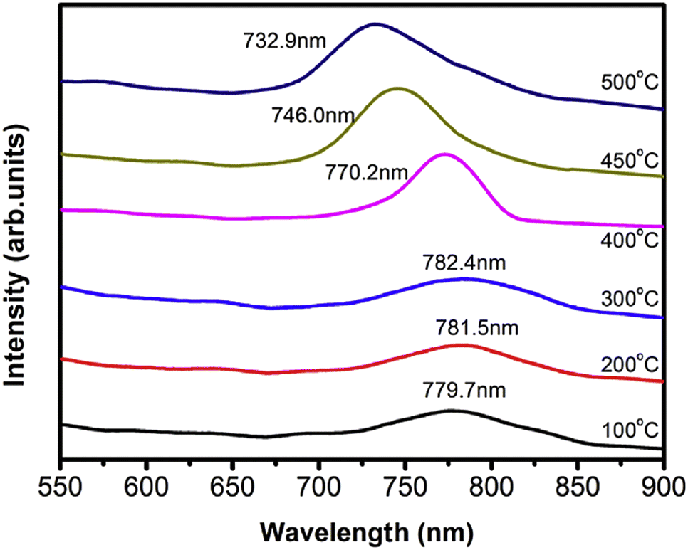 | ||
| Fig. 12 Photoluminescence spectra of CdZnTe thin films deposited at varied substrate temperatures. Reproduced from ref. 79 with permission, Copyright (2016), Elsevier. | ||
The normalized PL spectra of Cd1−xZnxTe films (x = 0.0–1.0) deposited via the MOCVD method were reported,88 where the reference PL spectra of the monocrystalline Cd1−xZnxTe films revealed the existence of the narrow and high intensity peaks corresponding to the band gap dealt recombination together with some wide and weaker intensity sub-band peaks owing to the defect-impurity associated recombination mechanism. Also, the normalized PL spectra of polycrystalline CdZnTe films revealed wide peaks due to the much higher defect-impurity recombination compared to the narrow peaks owing to the considerable plastic deformation in Cd1−xZnxTe films. The Raman and FTIR spectra of CSS-deposited Cd1−xZnxTe thin films having different Zn contents were measured,128 where the Raman spectra revealed the occurrence of Te (Al) phonons at the wavenumber of 116 cm−1 for all the compositions. In the case of CdTe films, the CdTe (1TO) + Te (E) phonon modes were observed at the wavenumber of 137 cm−1, for ZnTe films, the Te (E) phonon mode at the wavenumber of 137 cm−1 and the ZnTe (1LO) phonon mode at the wavenumber of 198 cm−1. The FTIR spectra of the Cd1−xZnxTe thin films showed the presence of two dominant absorption peaks at around 550 cm−1 and 825 cm−1 for all the concentrations. The first peak shifted towards a lower energy at 542 cm−1, which may be attributed to the shorter bond length of Zn–Te compared to that of Cd–Te.128
The effect of laser annealing on CZT films was studied by Raman spectroscopy, where annealing was performed using a micro-Raman IR laser. In the case of the pristine samples, as the concentration of Zn increased, the CdTe(LO1) mode was blue-shifted, whereas the ZnTe(LO1) mode was red-shifted. In the case of the annealed samples, the Te concentration was noteworthy and an A1(Te) mode of high intensity was observed and the intensity of the E(Te) mode also increased. The obtained results indicated that laser annealing led to an enhancement in the characteristics of the CZT films.141
In the case of CdZnTe thin films, the obtained Raman peaks should have high intensity and the corresponding modes should depict detailed information about the impact of the concentration of Cd, Zn and Te elements in CdZnTe thin films. Also, the intensity of the peaks depends on several factors such as quantity of sample, structural defects, and crystallinity. Therefore, the deposited films should have low defects, large grain size and high crystallinity to develop efficient devices. In the case of CdZnTe thin films, PL studies are based on their emission spectra, which should be comprised of strong emission lines and peaks of high intensity, indicating the presence of a small amount of crystal defects or imperfections. The FTIR spectra of CdZnTe thin films must demonstrate their actual chemical structure and the bonding present in the films efficiently.
An overview of the merits and drawbacks of the different characterization tools discussed in this review is depicted in Table 8.
| Technique(s) | Property | Merit(s) | Drawback(s) | Ref. |
|---|---|---|---|---|
| X-ray diffraction (XRD) | Structure and phase | • Provides information about structure and phase with: | • Not suitable for measuring small crystalline structures given that small structures present in trace amounts remain undetected in XRD measurements. | 142 |
| (a) Crystallinity. | ||||
| (b) Crystallite size. | ||||
| (c) Dislocation density. | ||||
| (d) Number of crystallites per unit area. | ||||
| (e) Internal strain. | ||||
| UV-Vis Spectrophotometry or UV-Vis NIR Spectrophotometry | Optical | • Useful for obtaining optical parameters such as: | • Requires careful operation given that factors such as electronic noise and outside contamination can influence measurements. | 143 |
| (a) Absorbance, transmittance and reflectance spectra. | ||||
| (b) Refractive index. | ||||
| (c) Extinction coefficient. | ||||
| (d) Optical energy band gap. | ||||
| Source meter/electrometer | Electrical | • Determines electrical parameters such as: | • Requires careful operation. | 144 |
| (a) Carrier concentration. | ||||
| (b) Mobility. | ||||
| (c) Conductivity. | ||||
| (d) Resistivity. | ||||
| Scanning electron microscopy (SEM) | Surface morphology | • Useful for obtaining morphological parameters such as: | • Requires high vacuum for samples those are non-conductive and volatile. | 145 |
| (a) Shape and size of grains of sample under observation. | ||||
| Transmission electron microscopy (TEM) | Surface morphology and structure | • Useful for obtaining micro-structural and morphological parameters such as: | • Ionizing radiation can damage samples used in TEM. | 146 |
| (a) Planes and orientations of sample surface. | • Destructive technique. | |||
| (b) Grain size. | ||||
| Atomic force microscopy (AFM) | Surface topography | • Provides information about: | • In comparison to SEM and TEM, AFM has a relatively slower scanning process. | 147 |
| (a) Surface roughness. | ||||
| (b) Root mean square (RMS) roughness. | ||||
| (c) Grain size. | ||||
| Energy dispersive spectroscopy (EDS) | Elemental or compositional | • Provides information about: | • Provides poor energy resolution of peaks. | 148 |
| (a) Elemental composition and concentration of different elements present in samples. | • Has low peak to Bremsstrahlung background ratio. | |||
| • Low detection limit to the lighter elements. |
Among the physical characterization tools depicted in Table 8, transmission electron microscopy is a destructive tool, while the other techniques are non-destructive, where the subjected sample can also be utilized in further measurements. Hence, the present section comprehensively described the different physical characteristics of individual CdZnTe thin films. The optimized conditions can be further applied in the development of CdZnTe thin film single-junction and tandem solar cells. The next section of the present review is dedicated to the development and characterization of the corresponding CdZnTe solar cell devices.
5. CdZnTe thin film-based solar cell devices
Nowadays, cost-effective and highly efficient CdTe thin film solar cells are the leading choice among research communities and industrialists based on their associated merits compared to drawbacks. By altering the thickness of the various layers used in CdTe-based devices and via various post-treatments, they may achieve a comparable performance to that of crystalline silicon (c-Si) solar cell devices. However, although CdTe-based devices have achieved a high efficiency of 22.1%, the requirement of an appropriate metal for rear contact in the superstrate configuration as lacking bears open circuit voltage loss, high recombination rate and density of surface states are the drawbacks those need to be overcome. Accordingly, to achieve this and exceed the efficiency limit of single-junction cells, CdZnTe has emerged as a promising material that can be applied as an absorber layer not only in single-junction thin film solar cells but also in tandem architectures owing to its high absorption coefficient, mobility and tunable band gap.117,149 CdZnTe thin film solar cells are fabricated with two configurations, either in the substrate (with architecture of metal substrate or metal coating substrate/p-CdZnTe/n-CdS/ITO/glass) structure or superstrate (with architecture Glass/ITO/CdS/CdZnTe/metal contact) structure. When a metal sheet or metallic-coated glass substrate with the desired dimensions as the base is employed, it is recognized as the substrate configuration, whereas the conducting transparent oxide-coated glass substrate comprising architecture is known as the superstrate configuration.50,150In both configurations in CdTe or CdZnTe devices, n-type CdS material is typically used as the window layer, which transmits the maximum incident light to the absorber layer, while the CdS optical window can also be replaced by a suitable layer considering cost effectiveness and environment friendly aspects.150Fig. 13(a) and (b) depict a pictorial view of the substrate and superstrate configurations. Fig. 13(c) shows the energy band diagram of a CdZnTe thin film-based solar cell device, explaining the position of the valence and conduction bands and metal contact work function. Also, the schematic structures together with energy levels and charge transfer mechanism in a CdZnTe based solar cell device is shown in Fig. 13(d) where transport layer engineering needs to be undertaken by materials evolution in order to enhance performance by reducing open circuit voltage loss. To establish a metal contact in these devices, either gold (Au) with copper (Cu) or silver (Ag) is used due to their good electrical conductivity and corrosion resistivity, where the combination of Cu with Au has been employed thus far in these devices given that Cu provides p-type doping in the CdTe layer and establishes better contact than pure Au and Ag materials.
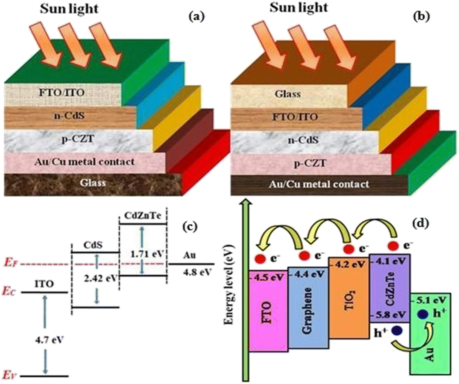 | ||
| Fig. 13 Typical device architecture in (a) substrate (where instead of metal coated glass, metal sheet could be employed) and (b) superstrate configurations (in both the architectures, Cd free environmental friendly optical window could also be applied but needs comparable performance), (c) energy band diagram and (d) schematic structures and energy levels of individual layers along with charge transfer mechanism in a CdZnTe thin film solar cell device, where (c) is reprinted with permission from ref. 151, Copyright (2018), Elsevier Ltd. | ||
To assess the performance of a solar cell device, the characteristic performance parameters, namely, short circuit current (Isc), short circuit current density (Jsc), open circuit voltage (Voc), fill factor (FF) and power conversion efficiency (η), are considered, which are typically obtained from current–voltage measurements performed under AM 1.5G illumination and standard test conditions of 25 °C temperature, where the incident solar power density is considered 100 mW cm−2 or 1000 W m−2 for simplicity. Further quantum efficiency (QE) measurements are performed to confirm the exact short circuit current.
The role of the CdS barrier reducing Zn loss during CdCl2 treatment of a CSS-deposited CdZnTe thin absorber layer was studied, and the results showed that the thin films of CdS acted as a barrier to prevent the escape of Zn during CdCl2 treatment. Also, the CdZnTe-based devices revealed Jsc, Voc, FF and η values of 12.5 mA cm−2, 0.60 V, 45% and 3.3%, respectively.132 CdZnTe-based solar cell devices having the architecture of ITO/CdS/CdZnTe/Au were fabricated using the vapor deposition technique,151 followed by treatment under vacuum and different annealing atmospheres, i.e., H2, N2 and Ar + O2. Among the devices, the findings revealed the highest PCE of 8.49% for the device annealed at 400 °C and treated in an Ar + O2 atmosphere. CdCl2-treated CdTe solar cell devices corresponding to different durations and CdZnTe solar cell devices having device architectures of ITO/CdS/CdTe/CdCl2/Cu-Au and FTO/CdS/CdZnTe/Cu-Au, respectively were fabricated employing the vapor evaporation technique152 and the associated performance parameters of Isc, Voc, FF and η were found to be 1.535 mA, 0.85 V, 66% and 8.11%, respectively. The CdCl2-treated CdTe solar cell devices demonstrated a slightly lower performance than the CdZnTe device. The QE characteristics of the CdTe solar cell device showed the photovoltaic nature of these cells with average peaks at 450 nm, 540 nm and 675 nm and the CdZnTe device revealed almost square-shaped behavior with average peaks at 440 nm and 625 nm.152
The influence of CdCl2 heat treatment on the ZnTe electron reflector layer was investigated in MOCVD-grown thin film CdTe solar cells153 and the associated performance parameters of Jsc, Voc, FF and η were determined to be 16 mA cm−2, 0.53 V, 40% and 3.4%, respectively. This study demonstrated that CdZnTe can be explored as an alternative electron reflector layer in solar cell devices. To explore impact of annealing and CdCl2 and ZnCl2 treatments on CdZnTe solar cells, devices were developed by incorporating a sputtered CdZnTe absorber,154 where the better photovoltaic performance was observed for the absorber treated and annealed at 430 °C, attaining Jsc, Voc, FF and η of 19 mA cm−2, 0.74 V, 51% and 7.2%, respectively. The efficiency was improved for the CdCl2- and ZnCl2-treated devices compared to the untreated devices, and thus annealing in hydrogen and argon atmospheres was performed to demonstrate the better device efficiency of the CdCl2- and ZnCl2-treated devices.
ZnTe and CdZnTe alloys were grown as the back contact on CdTe thin film solar cells,155 where CdZnTe and nitrogen-doped ZnTe layers were first grown on glass and GaAs substrates employing the MBE method, and later ZnTe films having a lower Zn to Te ratio were grown on CdTe thin films using the CSS method. For the device architecture of CdS/CdTe/Cd0.5Zn0.5Te:N/Au, Voc = 0.68 V, FF = 49%, η = 7.46% and Jsc = 22.60 mA cm−2 were obtained for a 0.2 μm-thick ZnTe layer. CdTe and CdZnTe solar cells were developed using the MOCVD and MBE methods in both the p–i–n and n–i–p configurations on glass/SnO2/CdS substrates and the effect of CdCl2 treatment on these solar cells was investigated. The PCE for the CdZnTe and CdTe solar cells was observed to be 4.4% and 10%, respectively. A higher PCE was attained for the CdTe solar cells, which may be due to the effective chloride treatment, promoting grain growth, reducing defects, and also improving the Jsc and Voc of the corresponding solar cell devices.156 CdTe and CdZnTe thin films were deposited on CdS/SnO2/glass substrates as the top subcell in tandem devices using the MOCVD and MBE methods, where the impact of annealing (in the range of 100–400 °C) on these films was explored.157 The Jsc, Voc, FF and η for the CdTe and CdZnTe solar cells were found to be in the range of 20.7–22.1 6 mA cm−2, 0.73–0.76 V, 59–72% and 9.7–10.8% and 3.21–14.4 mA cm−2, 0.429–0.646 V, 29–58% and 0.62–3.6%, respectively.157
Thus far, persistent efforts have been devoted for developing the high-performance solar cell devices comprised of CdZnTe absorber layers, but they are still far away from realizing performances to rival to the champion devices. Based on this review, Table 9 summarizes the performance parameters of the CdZnTe-based devices developed using various physical and chemical deposition techniques.
| Deposition techniques | Short circuit current density (Jsc) (mA cm−2) | Short circuit current (Isc) (mA) | Open circuit voltage (Voc) (V) | Fill factor (FF) (%) | Efficiency (η) (%) | Ref. |
|---|---|---|---|---|---|---|
| Close-space sublimation | 12.5 | — | 0.60 | 45 | 3.3 | 132 |
| Electron beam evaporation | — | 1.54 | 0.85 | 66 | 8.11 | 152 |
| Metal organic chemical vapor deposition | 16 | — | 0.53 | 40 | 3.4 | 153 |
| Sputtering | 19 | — | 0.74 | 51 | 7.2 | 154 |
| Molecular beam epitaxy | 22.6 | — | 0.68 | 49 | 7.46 | 155 |
Considering the above-mentioned detailed analysis on the work reported thus far on CdZnTe-based devices, herein, an n-type CdS window layer forms an asymmetric junction with the corresponding CdZnTe absorber layer to develop a suitable built-in-potential, which efficiently separates the generated charge carriers/excitons and drives them towards the respective electrodes to generate electricity. The window layer should be highly transparent to enable the maximum amount of sunlight to be transmitted to the absorber layer, i.e., no photocurrent generation should take place in the respective optical window layers. The p-type CdZnTe absorber layer should have a high absorption coefficient to absorb or harvest the maximum amount of incident sunlight transmitted by the window layer, followed by generating the maximum amount of charge carriers. Also, the solar cell parameters such as Jsc, Voc, FF and η of the corresponding device should be as high as possible as a consequence of the efficient conversion of sunlight into electricity. An advancement in the performance parameters of solar cells can be achieved by enhancing the quality of the CdZnTe layers via pre- and post-treatments such as doping, varying Zn concentration, annealing, and chloride activation.
Besides, although numerous simulation modeling tools have also been introduced to predict the performance to demonstrate high performance devices to meet the current energy demands together with compliance of global mandate for the production of energy with zero carbon emissions, these simulation tools do not consider the impact of grain boundaries, which are recognized as trap states and recombination centres those ultimately impact the performance of the devices, and thus experimental validation of the predicted performance is not possible.
6. Conclusion and future roadmap
The conversion of solar energy into electricity not only satisfies the demand of power generation but also contributes to tackling the severe climate change globally. However, although solar energy has been proven to be a major contributor in curbing environmental issues, there is a huge room for further improvement in the effective harvesting of sunlight and achieving the anticipated electrical power without harming the environment. Also, to address the issue of CO2 emission and satisfy the energy demand in a cost-effective manner, thin film solar cells have been emerged as potential candidates, wherein II–VI compound semiconductors are used to fabricate these devices due to their fascinating traits suitable for solar cell development.Among the II–VI compound semiconductors, CdTe has attracted significant attention owing to its desirable properties and CdTe-based thin film solar cells have significantly contributed to meeting the global power requirements. However, to reduce the parasitic resistance and open circuit voltage loss and enhance their photovoltaic performance, an alternative absorber is required. Accordingly, based on the present detailed review, an amalgamation of CdTe and ZnTe, i.e., CdZnTe, has been investigated in thin film solar cells due to its capable properties such as tunable energy band gap, high absorption coefficient and mobility, low leakage current and diverse lattice parameters. Despite the work done thus far, the required properties of CdZnTe thin films still have scope for enhancement for their application in single-junction and tandem devices not only in bearing mankind energy need but also satellite or space applications. However, although thin film technology has emerged and new technologies are being invented to develop cost-effective high-quality devices, there are still some drawbacks those need to be overcome. Drawbacks such as high production cost of PV modules, limited lifetime, material availability, life cycle constraints, efficiency, and toxicity are the future challenges for solar cell technology. Nevertheless, despite these issues, mature technologies for the preparation of CdZnTe thin films such as CdCl2 passivation, concentration evolution, post-annealing treatment, CdZnTe nanostructures, nanowires, quantum dots, and quantum wells have been employed thus far, which would be helpful in achieving the expected power conversion efficiency and open wider domains in the field of CdZnTe thin film solar cell devices in due course. Considering the above-mentioned facts, the present review provides useful insights, and also meticulously deals with the properties, physical and chemical deposition techniques and impact of thermal and chloride treatment and variation in zinc content on the physical characteristics of CdZnTe thin films and corresponding device development employing CdZnTe as the absorber layer.
To demonstrate high performances, CdZnTe-based solar cell devices need appropriate simulation modeling for designing suitable device architectures to predict a higher PCE for CZT-based single and tandem devices, which can be validated experimentally. Also, there are still many challenges in the development of highly efficient CZT-based single junction devices compared to the champion Si-based and competent perovskite solar cell devices considering the Shockley–Queisser limit. To break this limit, CZT-based tandem devices can be fabricated, wherein CZT can be applied as the top block. If CZT- and perovskite-based sub-cells are used as the top and bottom blocks, respectively, then the stability of perovskite solar cell devices may be enhanced due to the reduced degradation. Furthermore, the optical energy band gap of both CZT- and perovskite-based solar cells can be altered according to the needs of the developer by varying the concentrations of their constituent elements, and accordingly, high-PCE devices can be fabricated. Although the authors tried their best to incorporate almost all the available literature, they apologize if any work was inadvertently omitted.
Author contributions
All the authors have significantly contributed in the present review and therefore, they are credited for this review. The author wise credit is as under: Ritika Sharma: formal analysis, writing – original draft. Sakshi Chuhadiya: writing – original draft. Kamlesh: writing – original draft. Himanshu: writing – original draft. M. S. Dhaka: conceptualization, writing – original draft, supervision.Conflicts of interest
There are no conflicts of interest to declare.Acknowledgements
The authors sincerely acknowledge Department of Physics, Mohanlal Sukhadia University, Udaipur (India) and Ministry of Education, Government of India and Ministry of Higher Education, Government of Rajasthan, India through RUSA 2.0 Research and Innovation project for required financial support.References
- O. Ellabban, H. Abu-Rub and F. Blaabjerg, Renewable Sustainable Energy Rev., 2014, 39, 748–764 CrossRef.
- J. I. Kwak, S. H. Nam, L. Kim and Y. J. An, J. Hazard. Mater., 2020, 392, 122297 CrossRef CAS PubMed.
- A. A. Rockett, Curr. Opin. Solid State Mater. Sci., 2010, 14(6), 117–122 CrossRef.
- J. Nelson, Curr. Opin. Solid State Mater. Sci., 2002, 6(1), 87–95 CrossRef CAS.
- J. Nelson, The Physics of Solar Cells, Imperial College Press, 2002 Search PubMed.
- R. W. Birkmire and B. E. McCandless, Curr. Opin. Solid State Mater. Sci., 2010, 14(6), 139–142 CrossRef CAS.
- IRENA, Renewable Capacity Statistics, July 2023.
- M. L. Parisi, S. Maranghi, L. Vesce, A. Sinicropi, A. D. Carlo and R. Basosi, Renewable Sustainable Energy Rev., 2020, 121, 109703 CrossRef.
- V. Fthenakis, Renewable Sustainable Energy Rev., 2009, 13(9), 2746–2750 CrossRef CAS.
- A. J. McMichael, C. D. Butler and C. Folke, Science, 2003, 302(5652), 1919–1920 CrossRef CAS PubMed.
- S. K. Deb, Curr. Opin. Solid State Mater. Sci., 1998, 3, 31–59 CrossRef.
- D. J. Friedman, Curr. Opin. Solid State Mater. Sci., 2010, 14(6), 131–138 CrossRef CAS.
- W. Shockley and H. J. Queisser, J. Appl. Phys., 1961, 32, 510 CrossRef CAS.
- C. H. Henry, J. Appl. Phys., 1980, 51, 4494–4500 CrossRef CAS.
- S. Surabhi, K. Anurag and S. R. Kumar, Chalcogenide Lett., 2022, 19(2), 143–152 CrossRef CAS.
- N. A. Shah, W. Mahmood, M. Abbas, N. Nazar, A. H. Khosa, A. Zeb and A. Malik, RSC Adv., 2021, 11, 39940–39949 RSC.
- D. Zeng, D. Guo and X. Ren, Thin Solid Films, 2023, 768(1), 139685 CrossRef CAS.
- T. Li, Y. Shen, P. Sun, J. Huang, F. Gu, X. Liang, L. Wang and J. Min, Mater. Sci. Semicond. Process., 2023, 153, 107118 CrossRef CAS.
- X. Wan, Y. Li, T. Tan, Y. Liu, H. Wei, K. Cao and G. Zha, Mater. Sci. Semicond. Process., 2023, 153, 107158 CrossRef CAS.
- Y. V. Znamenshchykov, V. V. Kosyak, O. K. Kononov, I. O. Shpetnyi, V. I. Grebinaha, P. M. Fochuk and A. S. Opanasyuk, Vacuum, 2018, 149, 270–278 CrossRef CAS.
- S. Chander and M. S. Dhaka, Mater. Lett., 2017, 186, 45–48 CrossRef CAS.
- Y. Zhang, J. Huang, J. Zhang, Q. Mou, Y. Shen and L. Wang, Surf. Coat. Technol., 2016, 307, 1158–1161 CrossRef CAS.
- L. Li, Y. Xu, B. Zhang, A. Wang, J. Dong, H. Yu and W. Jie, Appl. Phys. Lett., 2018, 112, 112101 CrossRef.
- K. H. Kim, S. Hwang, P. Fochuk, L. Nasi, A. Zappettini, A. E. Bolotnikov and R. B. James, IEEE Trans. Nucl. Sci., 2016, 63(4), 2278–2282 CAS.
- U. N. Roy, R. M. Mundle, G. S. Camarda, Y. Cui, R. Gul, A. Hossain, G. Yang, A. K. Pradhan and R. B. James, Sci. Rep., 2016, 6, 26384 CrossRef CAS PubMed.
- S. U. Egarievwe, W. Chan, K. H. Kim, U. N. Roy, V. Sams, A. Hossain, A. Kassu and R. B. James, IEEE Trans. Nucl. Sci., 2016, 63(1), 236–245 CAS.
- Y. Zhang, L. Wang, J. Lai, J. Huang, J. Zhang, R. Xu and Y. Shen, IEEE International Conference on Optoelectronics and Microelectronics (ICOM), 2015, pp. 474–477 Search PubMed.
- Y. Shen, Y. Xu, J. Sun, Z. Zhang, J. Huang, M. Cao, F. Gu and L. Wang, Surf. Coat. Technol., 2019, 358, 900–906 CrossRef CAS.
- K. Davami, J. Pohl, M. Shaygan, N. Kheirabi, H. Faryabi, G. Cuniberti, J. S. Lee and M. Meyyappan, Nanoscale, 2013, 5, 932–935 RSC.
- E. V. Maistruk, I. G. Orletsky, M. I. Ilashchuk, I. P. Koziarskyi, D. P. Koziarskyi, P. D. Marianchuk and O. A. Parfenyuk, Semicond. Sci. Technol., 2019, 34(4), 045016 CrossRef CAS.
- I. G. Orletskyi, M. I. Ilashchuk, E. V. Maistruk, M. M. Solovan, P. D. Maryanchuk and S. V. Nichyi, Ukr. J. Phys., 2019, 64(2), 164–172 CrossRef.
- S. Rubio, N. V. Sochinskii, E. Repiso, Z. Tsybrii, F. Sizov, J. L. Plaza and E. Diéguez, J. Cryst. Grow., 2017, 457, 211–214 CrossRef CAS.
- F. F. Sizov, R. K. Savkina, A. B. Smirnov, R. S. Udovytska, V. P. Kladko, A. I. Gudymenko, N. V. Safryuk and O. S. Lytvyn, Phys. Solid State, 2014, 56(11), 2160–2165 CrossRef CAS.
- Q. Zheng, F. Dierre, V. Corregidor, J. Crocco, H. Bensalah, J. L. Plaza, E. Alves and E. Dieguez, Thin Solid Films, 2012, 525, 56–63 CrossRef CAS.
- S. S. Verma, Next generation solar cells, 2016, pp. 21–25 Search PubMed.
- S. E. Sofia, J. P. Mailoa, D. N. Weiss, B. J. Stanbery, T. Buonassisi and I. M. Peters, Nat. Energy, 2018, 3, 387–394 CrossRef.
- M. Powalla, S. Paetel, E. Ahlswede, R. Wuerz, C. D. Wessendorf and T. M. Friedlmeier, Appl. Phys. Rev., 2018, 5, 041602 Search PubMed.
- M. A. Green, Y. Hishikawa, W. Warta, E. D. Dunlop, D. H. Levi, J. H. Ebinger and A. W. Y. H. Baillie, Prog. Photovoltaic, 2017, 25, 668–676 CrossRef.
- T. D. Lee and A. U. Ebong, Renewable Sustainable Energy Rev., 2017, 70, 1286–1297 CrossRef CAS.
- M. A. Green, J. Mater. Sci.: Mater. Electron., 2007, 18, 15–19 CrossRef.
- E. Kabir, P. Kumar, S. Kumar, A. A. Adelodun and K. H. Kim, Renewable Sustainable Energy Rev., 2018, 82(1), 894–900 CrossRef.
- A. A. Ellakany, M. Abouelatta, A. Shaker, G. T. Sayah and M. E. Banna, J. Eng., 2017, 10, 574–576 CrossRef.
- M. Kurban and S. Erkoc, Phys. E: Low-Dimens. Syst. Nanostructures, 2017, 88, 243–251 CrossRef CAS.
- M. Kurban and S. Erkoc, Comput. Mater. Sci., 2016, 122, 295–300 CrossRef CAS.
- M. Kurban, O. B. Malcioglu and S. Erkoc, Chem. Phys., 2016, 464, 40–45 CrossRef CAS.
- Y. Zhang, L. Wang, K. Qin, R. Xu, J. Lai, J. Huang, J. Zhang, J. Min and Y. Xia, Mater. Res. Innovations, 2015, 19, S9-14–S9-16 CrossRef.
- R. Triboulet and P. Siffert, CdTe and Related Compounds; Physics, Defects, Hetero- and Nano-structures, Crystal Growth, Surfaces and Applications, Elsevier, Oxford, 2010 Search PubMed.
- K. L. Chopra and L. K. Malhotra, Thin Film Technology and Applications, Tata Mc-GrawHill Publishing Co. Ltd., 1985 Search PubMed.
- M. S. Dhaka, Recent trends in thin film technology, Kalpana Publications, India, 2015 Search PubMed.
- K. L. Chopra, P. D. Paulson and V. Dutta, Prog. Photovoltaic, 2004, 12, 69–92 CrossRef CAS.
- K. Seshan, Handbook of Thin-Film Deposition Processes and Techniques, Noyes Publication, 2nd edn, 2002 Search PubMed.
- S. Banerjee and A. K. Tyagi, Functional Materials Preparation, Processing and Applications, Elsevier Publications, 2012 Search PubMed.
- A. E. Al-salami, A. Dahshan and E. R. Shaaban, Optik, 2017, 150, 34–47 CrossRef CAS.
- S. Chander, A. Purohit, S. L. Patel and M. S. Dhaka, Phys. E Low Dimens. Syst. Nanostruct., 2017, 89, 29–32 CrossRef CAS.
- S. Chander and M. S. Dhaka, Thin Solid Films, 2017, 625, 131–137 CrossRef CAS.
- Y. V. Znamenshchykov, V. V. Kosyak, A. S. Opanasyuk and P. M. Fochuk, Proc. Int. Conf. Nanomater.: Appl. Prop., 2015, 4, 01NTF16 Search PubMed.
- G. Zha, H. Zhou, J. Gao, T. Wang and W. Jie, Vacuum, 2011, 86(3), 242–245 CrossRef CAS.
- K. Prabakar, S. K. Narayandass and D. Mangalaraj, J. Alloys Compd., 2004, 364(1–2), 23–28 CrossRef CAS.
- K. Prabakar, S. Venkatachalam, Y. L. Jeyachandran, S. K. Narayandass and D. Mangalaraj, Sol. Energy Mater. Sol. Cells, 2004, 81(4), 1–12 CrossRef CAS.
- R. Sharma, A. Sharma, Himanshu, A. Thakur, M. D. Kannan and M. S. Dhaka, Mater. Res. Bull., 2023, 163, 112214 CrossRef CAS.
- K. Bashir, N. Mehboob, A. Ali, A. Zaman, M. Ashraf, M. Lal, K. Althubeiti and M. Mushtaq, Mater. Lett., 2021, 304, 130737 CrossRef CAS.
- I. Haider, B. Khan, M. Ali, A. Shuja, A. F. Qureshi and Z. Ali, Mater. Sci. Semicond. Process., 2020, 114, 105074 CrossRef CAS.
- X. Gao, S. Zhu, X. Zhu, B. Zhao, H. Sun, D. Yang and P. Wangyang, J. Mater. Sci.: Mater. Electron., 2018, 29(10), 8313–8319 CrossRef CAS.
- G. Rajesh, N. Muthukumarasamy, D. Velauthapillai, K. Mohanta, V. Ragavendran and S. K. Batabyal, Mater. Res. Express, 2018, 5, 026412 CrossRef.
- X. Gao, X. Zhu, H. Sun, D. Yang, P. Wangyang and S. Zhu, J. Mater. Sci.: Mater. Electron., 2017, 28, 4467–4474 CrossRef CAS.
- D. Zeng, Y. Mu, J. Meng, W. Liu, F. Chen and H. Zhou, Surf. Eng., 2016, 32(3), 190–193 CrossRef CAS.
- T. M. Shimpi, J. M. Kephart, D. E. Swanson, A. H. Munshi, W. S. Sampath, A. Abbas and J. M. Walls, J. Vac. Sci. Technol., A, 2016, 34, 051202 CrossRef.
- G. Zha, Y. Lin, D. Zeng, T. Tan and W. Jie, Appl. Phys. Lett., 2015, 106, 062103 CrossRef.
- D. Zeng, Y. Mu, W. Liu, H. Zhou and F. Chen, Adv. Mater. Res., 2014, 941–944, 1288–1292 Search PubMed.
- S. Seyedmohammadi, M. J. DiNezza, S. Liu, P. King, E. G. LeBlanc, X. H. Zhao, C. Campbell, T. H. Myers, Y. H. Zhang and R. J. Malik, J. Cryst. Grow., 2015, 425, 181–185 CrossRef CAS.
- P. Gergaud, A. Jonchère, B. Amstatt, X. Baudry, D. Brellier and P. Ballet, J. Electron. Mater., 2012, 41, 2694–2699 CrossRef CAS.
- S. Yoo, J. Avendano, L. Delmar, S. Nama, M. Q. Lopez and H. Choi, Thin Solid Films, 2016, 612, 91–95 CrossRef CAS.
- A. Aydinli, A. Compaan, G. C. Puente and A. Mason, Solid State Commun., 1991, 80(7), 465–468 CrossRef CAS.
- J. Huang, Q. Gu, F. Yang, K. Tang, S. Gou, Z. Zhang, Y. Shen, J. Zhang, L. Wang and Y. Lu, Surf. Coat. Technol., 2019, 364, 444–448 CrossRef CAS.
- Z. Zhang, Y. Shen, Y. Xu, J. Huang, M. Cao, F. Gu and L. Wang, Vacuum, 2018, 152, 145–149 CrossRef CAS.
- K. Cao, W. Jie, G. Zha, T. Tan, Y. Li and R. Hu, J. Cryst. Grow., 2018, 498, 197–201 CrossRef CAS.
- K. Qin, H. Ji, J. Huang, K. Tang, Y. Shen, X. Zhang, M. Cao, J. Zhang, Y. Shen and L. Wang, Surf. Coat. Technol., 2017, 320, 366–370 CrossRef CAS.
- Y. Zhang, L. Wang, R. Xu, J. Huang, J. Tao, H. Meng, J. Zhang and J. Min, Appl. Surf. Sci., 2016, 388, 589–592 CrossRef CAS.
- Y. Wu, H. Xu, H. Ji, J. Huang, J. Zhang, Z. Fang, K. Tang, X. Liang, R. Xu and L. Wang, Vacuum, 2016, 132, 106–110 CrossRef CAS.
- N. Pandey, S. Tripathi, B. Kumar and D. K. Dwivedi, 5th IEEE Uttar Pradesh Section International Conference on Electrical, Electronics and Computer Engineering (UPCON), 2018 Search PubMed.
- N. F. Patel, S. A. Bhakhar, H. S. Jagani, G. K. Solanki and P. M. Pataniya, Opt. Mater., 2023, 136, 113403 CrossRef CAS.
- A. Lakhatia and R. J. M. Palma, Engineered Biomimicry, Elsevier Publications, 2013 Search PubMed.
- M. Ohring, The Materials Science of Thin Films, Academic Press, San Diego, 1992 Search PubMed.
- R. Kumar, G. Kumar, O. Al-Dossary and A. Umar, Mater. Express, 2015, 5(1), 3–23 CrossRef CAS.
- N. N. Nikitenkov, Modern Technologies for Creating the Thin-film Systems and Coatings, Intech Open Ltd., 2017 Search PubMed.
- P. A. Savale, Asian J. Res. Chem., 2018, 11(1), 195–205 CrossRef.
- J. R. Creighton and P. Ho, Chemical Vapor Deposition (#06682G), ASM International, 2001 Search PubMed.
- S. Stolyarova, F. Edelman, A. Chack, A. Berner, P. Werner, N. Zakharov, M. Vytrykhivsky, R. Beserman, R. Weil and Y. Nemirovsky, J. Phys. D: Appl. Phys., 2008, 41, 065402 CrossRef.
- F. Edelman, S. Stolyarova, A. Chack, N. Zakharov, P. Werner, R. Beserman, R. Weil and Y. Nemirovsky, Phys. Status Solidi B, 2002, 229(1), 141–144 CrossRef CAS.
- R. G. Solanki, Indian J. Pure Appl. Phys., 2010, 48, 133–135 CAS.
- N. B. Chaure, S. Chaure and R. K. Pandey, Electrochim. Acta, 2008, 54(2), 296–304 CrossRef CAS.
- A. Bansal and P. Rajaram, Mater. Lett., 2005, 59(28), 3666–3671 CrossRef CAS.
- I. Nasieka, L. Rashkovetskyi, O. Strilchuk and B. Danilchenko, Nucl. Instrum. Methods Phys. Res., Sect. A, 2011, 648(1), 290–292 CrossRef CAS.
- M. Henini, Molecular Beam Epitaxy: From research to mass production, Elsevier Publications, 2013 Search PubMed.
- S. Kasap and P. Capper, Springer Handbook of Electronic and Photonic Materials, Springer International Publishing AG, 2017 Search PubMed.
- X. Qi and J. L. MacManus-Driscoll, Curr. Opin. Solid State Mater. Sci., 2001, 5(4), 291–300 CrossRef CAS.
- I. M. Dharmadasa and J. Haigh, J. Electrochem. Soc., 2006, 153(1), G47–G52 CrossRef CAS.
- M. A. Carreon and V. V. Guliants, Ordered Porous Solids: Recent Advances and Prospects, Elsevier Publications, 2009 Search PubMed.
- R. Chen, Y. Shen, T. Li, J. Huang, F. Gu, X. Liang, M. Cao, L. Wang and J. Min, Vacuum, 2021, 193, 110484 CrossRef CAS.
- G. Kartopu, Q. Fan, O. Oklobia and S. J. C. Irvine, Appl. Surf. Sci., 2021, 540(2), 148452 CrossRef CAS.
- I. M. Dharmadasa, Coatings, 2014, 4, 282–304 CrossRef.
- A. Kampmann and D. Lincot, J. Electroanal. Chem., 1996, 418(1–2), 73–81 CrossRef CAS.
- D. E. Swanson, C. Reich, A. Abbas, T. Shimpi, H. Liu, F. A. Ponce, J. M. Walls, Y. H. Zhang, W. K. Metzger, W. S. Sampath and Z. C. Holman, J. Appl. Phys., 2018, 123, 203101 CrossRef.
- M. A. Sayeed and H. K. Rouf, Surf. Interfaces, 2021, 23, 100968 CrossRef CAS.
- W. L. Bragg, Proc. R. Soc. A, 1913, 89(610), 248–277 CAS.
- B. D. Cullity and S. R. Stock, Elements of X-Ray Diffraction, Prentice Hall, Inc., Upper Saddle River, New Jersey, U.S.A., 3rd edn, 2001 Search PubMed.
- J. Trevithick, J. Li, R. Ohno and C. A. Wolden, IEEE 43rd Photovoltaic Specialists Conference (PVSC), 2016, pp. 0518–0523 Search PubMed.
- C. Suryanarayan and M. G. Nortan, X-Ray Diffraction A Practical Approach, Plenum Press, New York, 1998 Search PubMed.
- P. Scherrer, Gottinger Nachr. Math. Phys., 1918, 2, 98–100 Search PubMed.
- U. Holzwarth and N. Gibson, Nat. Nanotechnol., 2011, 6(9), 534 CrossRef CAS PubMed.
- G. K. Williamson and R. E. Smallman, Philos. Mag., 1956, 1(1), 34–46 CrossRef CAS.
- S. Chander and M. S. Dhaka, Mater. Lett., 2016, 182, 98–101 CrossRef CAS.
- K. Cao, W. Jie, G. Zha, R. Hu, S. Wu and Y. Wang, Vaccum, 2019, 164, 319–324 CrossRef CAS.
- F. Yang, J. Huang, T. Zou, K. Tang, Z. Zhang, Y. Ma, S. Gou, Y. Shen, L. Wang and Y. Lu, Surf. Coat. Technol., 2019, 357, 575–579 CrossRef CAS.
- A. Y. Shenouda and M. M. Rashad, Mater. Res. Innovations, 2018, 23(6), 363–368 CrossRef.
- G. G. Rusu, M. Rusu and M. Girtan, Vacuum, 2007, 81(11–12), 1476–1479 CrossRef CAS.
- R. Sharma, Himanshu, S. L. Patel, M. D. Kannan and M. S. Dhaka, Surf. Interfaces, 2022, 33, 102204 CrossRef CAS.
- F. K. Alfadhili, G. K. Liyanage, A. B. Phillips and M. J. Heben, MRS Adv., 2018, 3(52), 3129–3134 CrossRef CAS.
- S. N. Moger, D. U. Shanubhogue, R. Keshav and M. G. Mahesha, Superlattices Microstruct., 2020, 142, 106521 CrossRef CAS.
- P. J. Worsfold and E. A. Zagatto, Encyclopedia of Analytical Science, Elsevier Publications, 2nd edn, 2017 Search PubMed.
- H. H. Perkampus, UV-Vis Spectroscopy and its Application, Springer-Verlag: Publications, 1992 Search PubMed.
- J. Tauc, Amorphous and Liquid Semiconductors, Springer, US, 1974 Search PubMed.
- S. Chander and M. S. Dhaka, Phys. E Low Dimens. Syst. Nanostruct., 2016, 84, 112–117 CrossRef CAS.
- R. Swanepoel, J. Phys. E: Sci. Instrum., 1983, 16(12), 1214–1222 CrossRef CAS.
- P. J. L. Herve and L. K. J. Vandamme, J. Appl. Phys., 1995, 77, 5476–5477 CrossRef CAS.
- M. Chakraborty and S. Bhattacharyya, Mater. Sci. Semicond. Process., 2016, 53, 47–55 CrossRef CAS.
- D. Zeng, W. Jie, H. Zhou, Y. Yang and F. Chen, Adv. Mater. Res., 2011, 194–196, 2312–2316 CAS.
- K. Chanthercrob, T. Gaewdang, N. Wongcharoen and C. P. Rakkiat, The 43rd Congress on Science and Technology of Thailand (STT 43), 2017 Search PubMed.
- C. R. Bundle, C. A. Evans Jr. and S. Wilson, Encyclopedia of Materials Characterization: Surfaces, Interfaces, Thin Films, Butterworth-Heinemann Inc. Publications, 1992 Search PubMed.
- I. Z. Jenei, Scanning electron microscopy (SEM) analysis of tribo-films enhanced by fullerene-like nanoparticles, thesis for the degree of Licentiate in Physics, Stockholm University, Sweden, 2012 Search PubMed.
- S. Wang, Surface characterization of chemically modified fiber, wood and paper, PhD thesis, Abo Akademi University, Finland, 2014 Search PubMed.
- T. M. Shimpi, D. E. Swanson, J. Drayton, A. Abbas, J. M. Walls, K. L. Barth and W. S. Sampath, Sol. Energy, 2018, 173, 1181–1188 CrossRef CAS.
- S. J. Bell, M. A. Baker, D. D. Duarte, A. Schneider, P. Seller, P. J. Sellin, M. C. Veale and M. D. Wilson, Appl. Surf. Sci., 2018, 427, 1257–1270 CrossRef CAS.
- R. N. Jagpat and A. H. Ambre, Indian J. Eng. Mater. Sci., 2006, 13(4), 368–384 Search PubMed.
- M. Hrouzek, Atomic Force Microscopy, modeling, estimation and control, PhD thesis, Universite Fourier-Joseph Grenoble and Brno University of Technology, France, 2007 Search PubMed.
- D. K. Schroder, Semiconductor material and device characterization, IEEE Press Wiley, 2006 Search PubMed.
- M. L. Kioko, Characterization of SnxSey/ZnO:Sn p–n Junction For Solar Cell Applications, PhD thesis, School of Pure and Applied Sciences, Kenyatta University, Nairobi-Kenya, 2011 Search PubMed.
- J. C. Russ, Fundamentals of Energy Dispersive X-ray Analysis, Butterworths & Co Publishers Ltd., 1984 Search PubMed.
- S. K. Pradhan, A Project Report on Liquid Fuel from Oil Seeds by Pyrolysis, National Institute of Technology, Rourkela, India, 2012 Search PubMed.
- S. N. Vidhya, O. N. Balasundaram and M. Chandramohan, Optik, 2015, 126(24), 5460–5463 CrossRef CAS.
- Y. V. Znamenschhykov, V. V. Kosyak, A. S. Opanasyuk, A. Stanislavov, V. Kuznetsov and Y. P. Gnatenko, Proc. Int. Conf. Nanomater.: Appl. Prop., 2014, 3, 01NTF24 Search PubMed.
- https://sciencing.com/advantages-disadvantages-xrd-xrf-6054766.html, Retrieved in March, 2023.
- https://sciencing.com/advantages-disadvantages-uvvis-spectrometer-6466475.html, Retrieved in March, 2023.
- https://download.tek.com/document/SMU+RnD_eguide2514.pdf, Retrieved in March, 2023.
- https://www.innovatechlabs.com/newsroom/2083/advantages-disadvantages-scanning-electron-microscopy/, Retrieved in March, 2023.
- https://www.news-medical.net/life-sciences/Limitations-of-TEM.aspx, Retrieved in March, 2022.
- https://www.microscopemaster.com/atomic-force-microscope.html, Retrieved in March, 2022.
- https://www.globalsino.com/EM/page4661.html, Retrieved in March, 2023.
- S. Chander and S. K. Tripathi, Adv. Mater. Interfaces, 2023, 10(28), 2300327 CrossRef CAS.
- A. Romeo and E. Artegiani, Energies, 2021, 14(6), 1684 CrossRef CAS.
- S. Chander, A. K. De and M. S. Dhaka, Sol. Energy, 2018, 174, 757–761 CrossRef CAS.
- S. Chander and M. S. Dhaka, Sol. Energy, 2017, 150, 577–583 CrossRef CAS.
- D. Mohanty, P. Y. Su, G. C. Wang, T. M. Lu and I. B. Bhat, Sol. Energy, 2016, 135, 209–214 CrossRef CAS.
- S. H. Lee, A. Gupta and A. D. Compaan, Phys. Status Solidi C, 2004, 1(4), 1042–1045 CrossRef.
- N. Amin, A. Yamada and M. Konagai, Jpn J. Appl. Phys., 2002, 41, 2834–2841 CrossRef CAS.
- A. Rohatgi, R. Sudharsanan, S. A. Ringel and M. H. M. Dougal, Sol. Cells, 1991, 30(1–4), 109–122 CrossRef CAS.
- A. Rohatgi, S. A. Ringel, R. Sudharsanan, P. V. Meyers, C. H. Liu and V. Ramanathan, Sol. Cells, 1989, 27(1–4), 219–230 CrossRef CAS.
| This journal is © The Royal Society of Chemistry 2023 |