
 Open Access Article
 This Open Access Article is licensed under a Creative Commons Attribution-Non Commercial 3.0 Unported Licence
Planar micro-supercapacitors toward high performance energy storage devices: design, application and prospects
Shifan
Zhu†
 a,
Zhiheng
Xu†
bc,
Haijun
Tao
*d,
Dandan
Yang
e,
Xiaobin
Tang
*bc and
Yuqiao
Wang
*a
a,
Zhiheng
Xu†
bc,
Haijun
Tao
*d,
Dandan
Yang
e,
Xiaobin
Tang
*bc and
Yuqiao
Wang
*a
aResearch Center for Nano Photoelectrochemistry and Devices, School of Chemistry and Chemical Engineering, Southeast University, Nanjing 211189, China. E-mail: yqwang@seu.edu.cn
bDepartment of Nuclear Science and Technology, Nanjing University of Aeronautics and Astronautics, Nanjing 211106, China. E-mail: tangxiaobin@nuaa.edu.cn
cKey Laboratory of Nuclear Technology Application and Radiation Protection in Astronautics, Ministry of Industry and Information Technology, Nanjing 211106, China
dJiangsu Key Laboratory of Materials and Technology for Energy Conversion, College of Material Science and Technology, Nanjing University of Aeronautics and Astronautics, Nanjing 211100, China. E-mail: taohaijun@nuaa.edu.cn
eSchool of Chemistry and Chemical Engineering, Yangzhou University, Yangzhou 225002, China
First published on 1st May 2023
Abstract
The burgeoning revolutions of portable and integrated electronic products have drastically stimulated the upgrade of traditional power supplies toward miniaturized scales. In this regard, planar micro-supercapacitors (PMSCs) are considered as candidates for energy storage devices owing to the unique two-dimensional structure, fast charge/discharge rate, high power density and long cycling lifetime. However, the manufacturing of PMSCs requires advanced techniques to provide rational designs on microelectrodes and reduce the size while maintaining high-resolution. The vacuum filtration and spray coating techniques have been used to design millimeter-scale electrodes with the assistance of an interdigital mask. The electrochemical strategy and other mask-free techniques can further reduce the size of the microelectrodes and meet the requirements of high-resolution PMSCs, including electrolytic and electrophoretic deposition, inkjet printing, laser scribing, plasma jet, nanoimprint lithography and 3D printing techniques. The precise design of PMSCs contributes to energy storage devices, sensors and filters. Furthermore, it is vital to design a microelectrode with superior structural integrity for the controllable manufacture of high precision and high performance PMSCs by considering the mechanism and key factors of microfabrication strategies.
 Shifan Zhu | Shifan Zhu received his BS degree in Mineral Process Engineering from China University of Mining and Technology. He is currently pursuing his PhD degree in Physics & Chemistry on Materials in Southeast University, Nanjing, China. His research interests focus on the energy materials, electrochemical reaction kinetics and device integration. |
 Zhiheng Xu | Zhiheng Xu received his BS degree in Nuclear Engineering and Technology from East China University of Technology, and MS and PhD in Nuclear Technology and Materials Engineering from Nanjing University of Aeronautics and Astronautics. Now, he is an associate research fellow working at Nanjing University of Aeronautics and Astronautics. His current research interests focus on energy conversion technologies and their applications, preparation and performance characterization of new energy materials and devices. |
 Haijun Tao | Haijun Tao received his BS degree in Materials Science from Nanjing University of Aeronautics and Astronautics, and MS and PhD in Materials Science and Engineering from Nanjing University of Aeronautics and Astronautics. Now, he is a Full Associate Professor at Nanjing University of Aeronautics and Astronautics. His current research interests focus on photovoltaic materials and devices and recycling of new energy materials. |
 Dandan Yang | Dandan Yang received her BS degree in Chemical Engineering and Technology from Luoyang Normal University, MS in Chemical Engineering from Nanjing University of Technology, and PhD in Materials Science and Engineering from Nanjing University of Science and Technology. Now, she is a lecturer at Yangzhou University. Her current research interests focus on surface design, optical performance optimization, stability improvement and optoelectronic applications of metal halide nanocrystals. |
 Xiaobin Tang | Xiaobin Tang received his BS, MS and PhD degrees from Nanjing University of Aeronautics and Astronautics. Now, he is a Full Professor at Nanjing University of Aeronautics and Astronautics, who is also the Deputy Dean of the College of Materials Science and Technology, the head of discipline and specialty, and the director of the Key Laboratory of the Ministry of Industry and Information Technology for Space Nuclear Technology Application and Radiation Protection. His current research interests focus on new energy technologies and materials, electrical stability of electronic components, and nuclear instrumentation development. |
 Yuqiao Wang | Yuqiao Wang received his BS degree from Anhui University, and MS and PhD degrees from Southeast University. Now, he is a Full Professor at Southeast University, who is also the Head of Research Center for Nano Photoelectrochemistry & Devices. His current research interests focus on energy and environmental materials, photoelectrochemical reaction mechanism, device integration, and the relationship between material invalidation and device performance attenuation. |
1. Introduction
The emerging miniaturized electronic components have become an integral part of the Internet of Things (IoTs), concomitantly leading to the renovation of traditional energy storage supplies to reduce the size without sacrificing the power and energy densities.1–3 In particular, wearable electronics, biomedical sensors and renewable energy grids can facilitate the miniaturization and integration of energy storage systems.4,5 Lithium-ion batteries (LIBs) and supercapacitors (SCs) are commonly used as the energy storage components in different fields depending on their intrinsically high energy and power densities, respectively. However, the limited lifetime and power density of LIBs may restrain their widespread application for on-chip electronics as well as be a bottleneck in micro-sized and integrated systems. Compared with LIBs, SCs can deliver long-term stability and meet the high-power requirements in automatic systems, intelligent grids and rail traffic.6–8 However, the integration of traditional SCs in a miniaturized module is commonly restricted by their large space occupancy and unsatisfactory integration capabilities. Therefore, it is expected that micro-sized energy storage devices with fertile energy and power densities will be designed and manufactured for the next generation of power supplies.Recently, micro-supercapacitors (MSCs), especially planar micro-supercapacitors (PMSCs), have been considered as one of the candidates for traditional energy storage devices due to their unique two-dimensional structure, fast charge/discharge rate, high power density and long-term stability. The size of PMSCs can be reduced to several millimeters and even micrometers, and the corresponding planar configuration is evidently different from the conventional sandwich-like SCs.9–11 The unique in-plane structure enables the integration of the monolithic device into the overall system with low space occupancy. The ion transport inside the PMSCs can be drastically accelerated owing to the interdigital structure of the planar microelectrodes.12–14 The ion diffusion distance between the negative and positive electrodes can be shortened to several micrometers, which endows fast ionic diffusion kinetics for high-rate capability.15,16 PMSCs can be assembled into micro-integrated systems over conventional energy storage components.17 However, the technique of fabricating PMSCs remains a critical hurdle due to the complicated process. Recent reports have tended to reduce the electrode size and shorten the gap between adjacent electrodes, while retaining the high-resolution of the PMSCs simultaneously. The design strategies of MSCs have been extensively reviewed in relevant literature.18–20 Researchers have focused on the recent progress in advanced techniques to demonstrate the practicality of diverse manufacturing strategies. The manufacturing strategies determine the size and precision of the microelectrodes based on the guidance of the interdigital mask. Hence, it is necessary to develop suitable design strategies for the desired PMSCs through in-depth analysis and comparison of different fabrication techniques.
Herein, we discussed the basic configurations, energy storage mechanisms and fabrication techniques of PMSCs in comparison with conventional SCs. The rational design of microelectrodes plays a key role in the manufacture of high-resolution PMSCs. For vacuum filtration and spray coating techniques, the interdigital mask can be designed as a structured guidance for the fabrication of millimeter-scale electrodes. Further reduction in the size of the microelectrodes can be achieved by electrolytic and electrophoretic deposition, inkjet printing, laser scribing, plasma jet, nanoimprint lithography and 3D printing techniques. The well-designed PMSCs with high resolution and structural integrity can be used as energy storage devices, sensors and filters (Fig. 1).
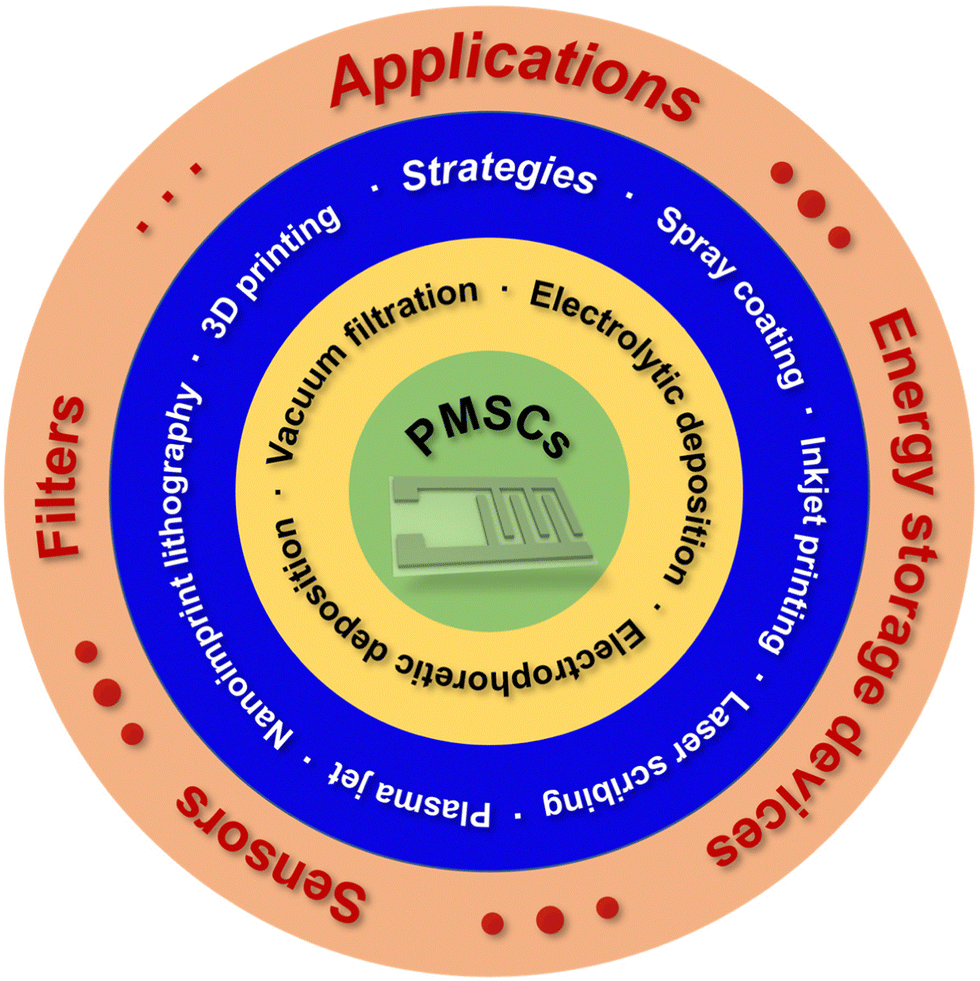 | ||
| Fig. 1 Schematic diagram of the contents of this review, including strategies for constructing PMSCs and corresponding applications. | ||
2. Configuration and energy storage mechanism of PMSCs
The basic configuration of PMSCs consists of four coplanar parts, including a positive and a negative electrode, a gel or solid-state electrolyte, and a substrate. Whether the current collector is needed depends on the electrical conductivity of the electrode materials.21,22 Carbon-based materials generally deliver a decent metalloid electron conductivity of 103–107 S m−1, enabling carbon-based electrodes to be an alternative to the current collector.23 Meanwhile, metal oxides and hydroxides commonly suffer from inferior electric conductivities (10−1–10−5 S m−1). Therefore, the conductive substrate in PMSCs is necessary for a high charge-transfer efficiency.24 In addition, electrode materials utilized in PMSCs are basically in accordance with conventional SCs, which can be divided into two types based on the charge storage mechanisms: (1) electric double layered capacitor (EDLC) type materials, relying on the mechanism of ion adsorption/desorption on the surface of electrodes; (2) pseudocapacitive materials, depending on the reversible faradaic redox reaction between the electrodes and electrolyte ions.25 Basically, the specific capacitance of pseudocapacitive materials, such as metal oxides and hydroxides, is higher than that of EDLC type materials (such as the carbon-based materials) owing to the fast reversible faradaic redox reactions.26–28 However, the universal drawback of PMSCs and SCs is the unsatisfactory energy density in comparison with batteries. Various approaches have been dedicated to tackling the issue according to the equation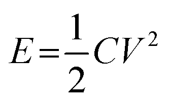 . The energy density (E) can be directly enhanced via improving the specific capacitance (C) of electrode materials and expanding the potential window (V). In this regard, pseudocapacitive materials may be employed to push the energy density towards a higher level due to the intrinsically superior capacitance. Besides, the potential window can be expanded by assembling an asymmetric device to match the operating voltage of pseudocapacitive materials and EDLC materials for an enhanced energy density.29–31
The electrolytes used in PMSCs are mainly divided into two types, namely gel polymers and ionic liquids. Conventional aqueous electrolytes, including KOH, H2SO4 and Na2SO4, have a risk of leakage in planar devices as well as a limitation in potential window (below 1.23 V) due to water electrolysis.32 Meanwhile, gel polymer electrolytes have been demonstrated to be excellent electrolytes for PMSCs. In general, poly (vinyl alcohol) (PVA) is used as the host polymer to mix with acid, alkali, and neutral-based electrolytes.33–35 The solvent evaporation and poor thermal stability are the main disadvantages of gel polymer electrolytes. To this end, ionic liquids have garnered tremendous attention recently for their fair stability and high operating voltage (up to 3.7 V).36,37 The superior stability arises from the combination of ionic liquids and the silica matrix in polycondensation processes. Therefore, the selection of an appropriate electrolyte is critical for optimizing the energy storage capabilities and ensuring long-term cycling stability of PMSCs.
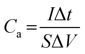
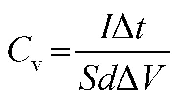
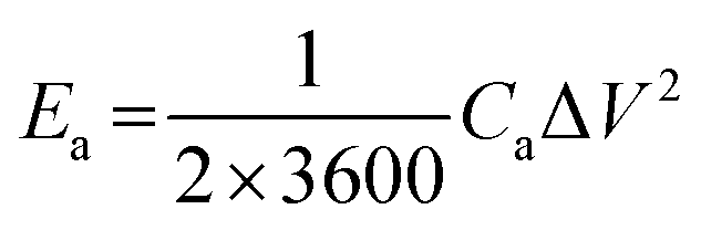
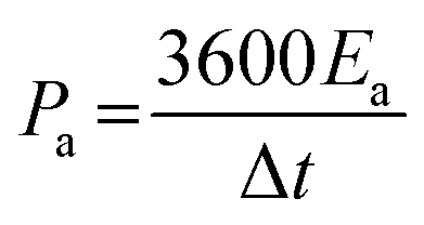
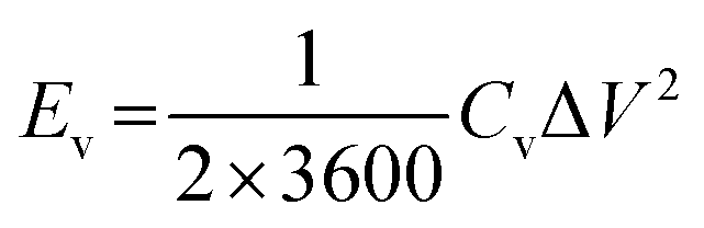
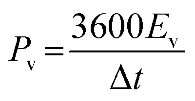
To cater for the requirements of high mechanical stability and flexibility, substrates used in the PMSCs can be classified into two categories. The first category is rigid substrates, such as silicon wafers, which are promising candidates for on-chip electronics.27,38,39 As the second category, flexible substrates (polymer, paper, and textile cloth) have been incorporated into foldable and wearable devices.40–43 To evaluate the electrochemical performance of PMSCs, conventional test parameters should be finely tuned based on the planar configuration. The measurement units need to be changed to the area and volume of PMSCs instead of the mass of active materials. Generally, the areal capacitance (Ca, mF cm−2) and volumetric capacitance (Cv, mF cm−3) can be calculated by eqn (1) and (2), while the areal energy density (Ea, mW h cm−2) and power density (Pa, mW cm−2) of PMSCs can be obtained viaeqn (3) and (4). The volumetric energy density (Ev, mW h cm−3) and power density (Pv, mW cm−3) can be calculated through eqn (5) and (6), respectively.20,44,45
 | (1) |
 | (2) |
 | (3) |
 | (4) |
 | (5) |
 | (6) |
The areal mass loading of the active material determines the energy storage capability of PMSCs. The higher mass loading can contribute to the improved Ca on considering two devices with equal area. However, the device resistance (R) may also increase with the mass loading, leading to a deteriorated time constant (τ) according to eqn (7).11,16,19
| τ = RCa | (7) |
The power performance of PMSCs is closely related to τ. A high value of τ can result in decreased power performance. Hence, it is crucial to explore materials with high conductivity for lowering the τ to improve the power performance and enhance the energy capability of PMSCs.
3. Preparation strategies of PMSCs
The trend towards miniaturized and integrated electronics has greatly stimulated the development of techniques for designing PMSCs. A variety of approaches have been dedicated to the manufacture of micro-sized electrodes. The challenge is to reduce the adjacent distance of interdigital electrodes and ensure the device has a high resolution simultaneously.32,46 In this regard, the vacuum filtration and spray coating techniques can fabricate millimeter-sized electrodes with the assistance of masks, which are designed by laser cutting technology with a hollow interdigital structure. The electrochemical strategies can reduce the size of PMSCs to the micrometer-scale without using masks. The inkjet printing, laser scribing, plasma jet, nanoimprint lithography and 3D printing techniques can also be applied to design and manufacture miniaturized PMSCs. The working conditions of each technique determine their feasibility for large-scale fabrication and precise design of monolithic devices.3.1 Mask-assisted strategies
 | ||
| Fig. 2 Vacuum filtration of electrode material suspensions to construct PMSCs. (a) Schematic illustration of the fabrication process of nano-sandwiched MHCF/graphene (M = Cu, Ni, Co, Fe) PMSCs on the PET substrate and the corresponding photograph. Reproduced with permission.48 Copyright 2019, Royal Society of Chemistry. (b) Schematic illustrating the fabrication process of the Ti3C2Tx/MnO2-based PMSCs. Reproduced with permission.49 Copyright 2020, IOP. (c) Schematic preparation process of VN‖MnO2-AMSCs. Reproduced with permission.50 Copyright 2018, Elsevier. (d) Mask-assisted construction process of COF-MSC and the corresponding optical photograph. Reproduced with permission.53 Copyright 2019, Wiley-VCH. | ||
Furthermore, the vacuum filtration strategy can be used to manufacture asymmetric electrodes with the assistance of pre-designed positive and negative masks. After the filtration of exfoliated graphene (EG) as the current collector, the porous VN and mesoporous MnO2 were successively filtrated as the negative and positive electrodes, respectively (Fig. 2(c)).50 The VN‖MnO2 based PMSC was assembled by using a novel “water-in-salt” gel of SiO2–lithium bis(trifluoromethane sulfonyl)imide (LiTFSI) as the electrolyte. The device delivered a voltage window of 2.0 V due to the asymmetric configuration. Meanwhile, the porous VN and MnO2 can accelerate the electrolyte ion transportation in plane for enhanced diffusion kinetics.51,52 Apart from this asymmetric configuration, the symmetric covalent organic framework (COF)-based MSC was fabricated through a one-step mask-assisted vacuum filtration strategy (Fig. 2(d)).53 The assembled MSC exhibited a thickness of 3 μm and showed an excellent flexibility by using the PET substrate and LiCl/PVA gel electrolyte.
To sum up, vacuum filtration is a simple strategy to manufacture thickness-controlled PMSCs without time-consuming processes. However, the size of the electrode is critically determined by the pre-designed mask. The adjacent distance between interdigital electrodes is commonly several millimeters in width. The reduction of the size from millimeters to micrometers remains a great challenge owing to the possibility of crosslinking between interdigital electrodes during filtration processes. Therefore, the vacuum filtration strategy is suitable for the fast and scalable fabrication of PMSCs, which have no specific requirements for micro-sized and high-resolution devices.
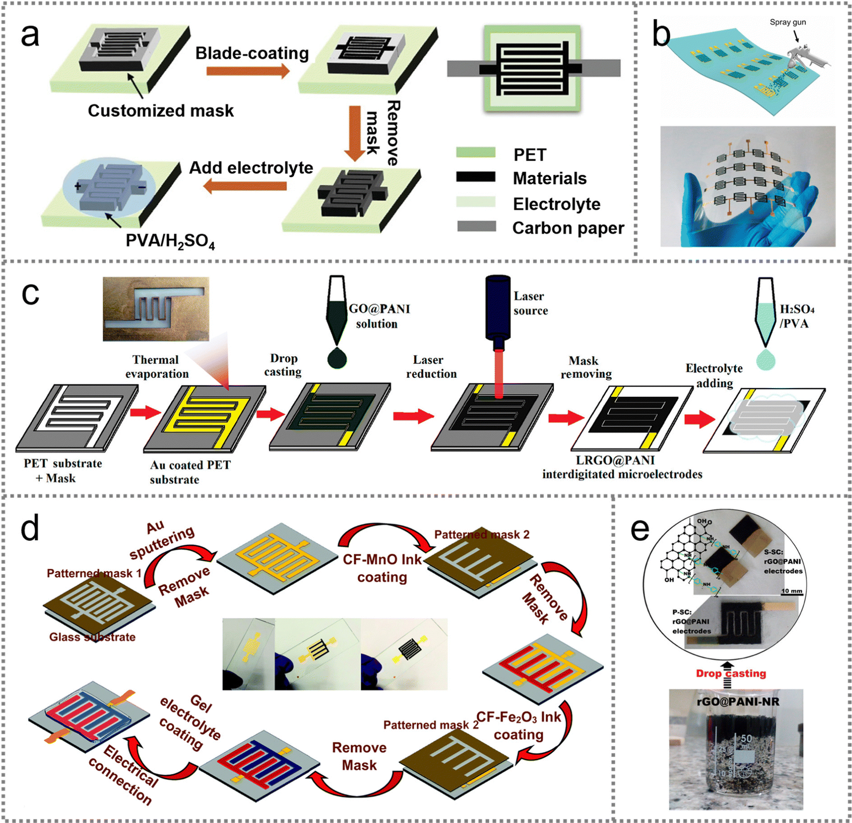 | ||
| Fig. 3 Spray coating strategy for PMSC fabrication. (a) Schematic illustration of the mask-assisted preparation process of PMSCs and the corresponding configuration. Reproduced with permission.55 Copyright 2019, Wiley-VCH. (b) Illustration of a spray coating method to construct PMSC arrays. Reproduced with permission.56 Copyright 2021, Elsevier. (c) Schematic illustration of the fabrication process for LRGO@PANI-MSC. Reproduced with permission.57 Copyright 2020, American Chemical Society. (d) Schematic illustrating the procedure of solid-state PMSCs on a glass substrate. Reproduced with permission.58 Copyright 2021, Royal Society of Chemistry. (e) Digital photographs of the rGO@PANI-NR nanocomposite for fabricating electrodes. Reproduced with permission.59 Copyright 2021, American Chemical Society. | ||
An interdigital Au electrode can be designed by the thermal evaporation technique on a PET substrate to facilitate the electron transfer and improve the conductivity of the device. Then, the graphene oxide@polyaniline (GO@PANI) ink was drop cast on the interdigital Au current collector followed by in situ laser reduction for fabricating LRGO@PANI PMSC (Fig. 3(c)).57 The assembled symmetric PMSC presented a 13 times higher areal capacitance of 72 mF cm−2 than that of the RGO-based device at the current density of 35 μA cm−2. As an effective strategy to improve the electrochemical performance, the asymmetric PMSCs can also be constructed by coating methods. The carbon foam (CF)-based asymmetric PMSC was designed to exhibit a wide potential window of 1.4 V by using CF–MnO as the positive and CF–Fe2O3 as the negative electrode on a glass substrate (Fig. 3(d)).58 Three types of interdigital stainless-steel masks with different patterns assisted the coating of the Au current collector, positive electrode and negative electrode, respectively. The in-plane configuration of the PMSCs enabled fast ion transport and charge transfer for the superior rate capability. The RGO@PANI nanorod composite-derived PMSCs showed higher energy and power densities than those of sandwich structured SCs (Fig. 3(e)).59
Generally, the spray coating strategy can fabricate PMSCs on a large scale with simple procedures. The active materials can be directly coated on the substrates with the guidance of interdigital masks. However, the low homogeneity of the slurry has a negative effect on the uniformity of the microelectrodes. The weak adhesion between the electrodes and substrate hinders their long-term stability. Therefore, the exploration of homogenous slurries is expected to enhance the affinity with substrates for fabricating high-performance devices.
3.2 Strategies without using masks
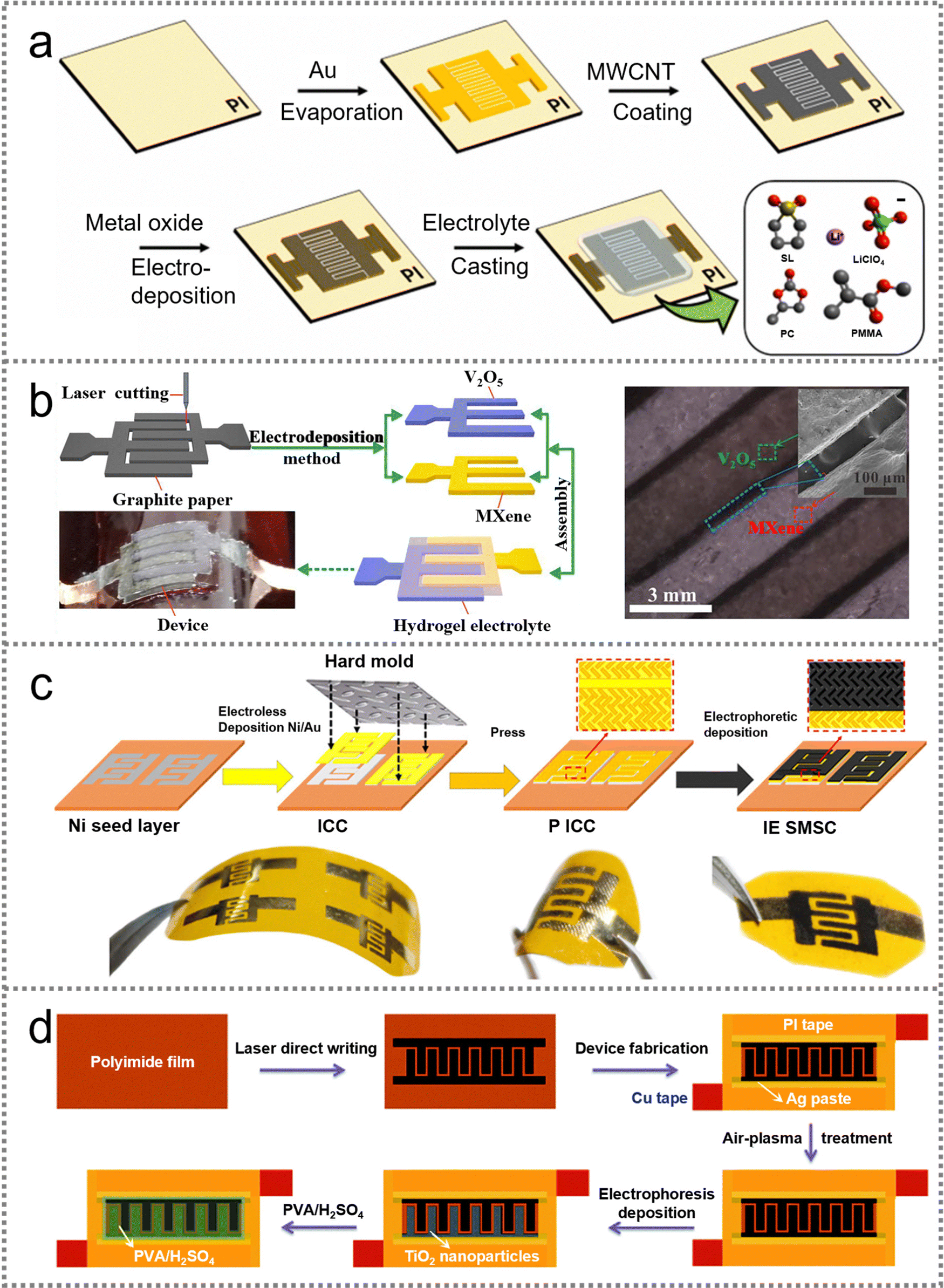 | ||
| Fig. 4 PMSC fabrication by an electrolytic and electrophoretic deposition strategy. (a) Schematic illustration of the fabrication process of a flexible PMSC. Reproduced with permission.62 Copyright 2021, Elsevier. (b) Schematic diagram of the preparation and assembly process of the ZIHMSC and the corresponding SEM image. Reproduced with permission.63 Copyright 2021, Elsevier. (c) Schematic preparation procedures of IE SMSCs. Reproduced with permission.64 Copyright 2019, American Chemical Society. (d) Illustration of the construction process of a carbon/TiO2 PMSC. Reproduced with permission.65 Copyright 2017, Royal Society of Chemistry. | ||
As an alternative strategy to electrolytic deposition, electrophoretic deposition has been deemed as another effective electrochemical method to construct interdigital electrodes. The charged nanosheets, nanoparticles, and nanorods can diffuse toward the current collector under the electric field force for further deposition. In Fig. 4(b), the charged Ti3C2Tx nanosheets were electrophoretically deposited onto the finger-structure graphite paper as the anode under the potential of 20 V. The interdigital current collector (ICC) also plays a significant role in guiding the electrophoretic deposition process as the forementioned electrolytic deposition strategy (Fig. 4(c)).64 The patterned Ni seed layer was deposited with Ni and Au to serve as the ICC for the fabrication of an interfacial enhanced active carbon symmetrical MSC (IE SMSC). The interdigital electrode presented a finger width of 500 μm and interspace of 300 μm, demonstrating the feasibility of the electrochemical strategy in the reduction of electrode size from millimeter to micrometer-scale in comparison to the mask-assisted techniques. In the case of charged nanoparticles, the asymmetric carbon‖carbon/TiO2 PMSC was fabricated with the electrophoretic deposition method on a PI substrate (Fig. 4(d)).65 The micro-scale interdigital pattern was designed via laser direct writing followed by air-plasma etching for the hydrophilic surface, which was conducive to the deposition of TiO2 nanoparticles on the substrate.
The electrochemical strategies exhibit simple procedures to obtain controllable thickness and reduced size of interdigital electrodes. However, the uncontrollable growth in the lateral direction can lead to the deteriorated resolution of the electrolytic deposited electrode owing to the decreased interspace. For the electrophoretic deposition strategy, the active materials are required to be electrically charged for directional migration to the conductive substrate under the electric field. Meanwhile, the fabricated electrodes may suffer from poor stability due to the weak adhesion between the deposited materials and conductive substrates.
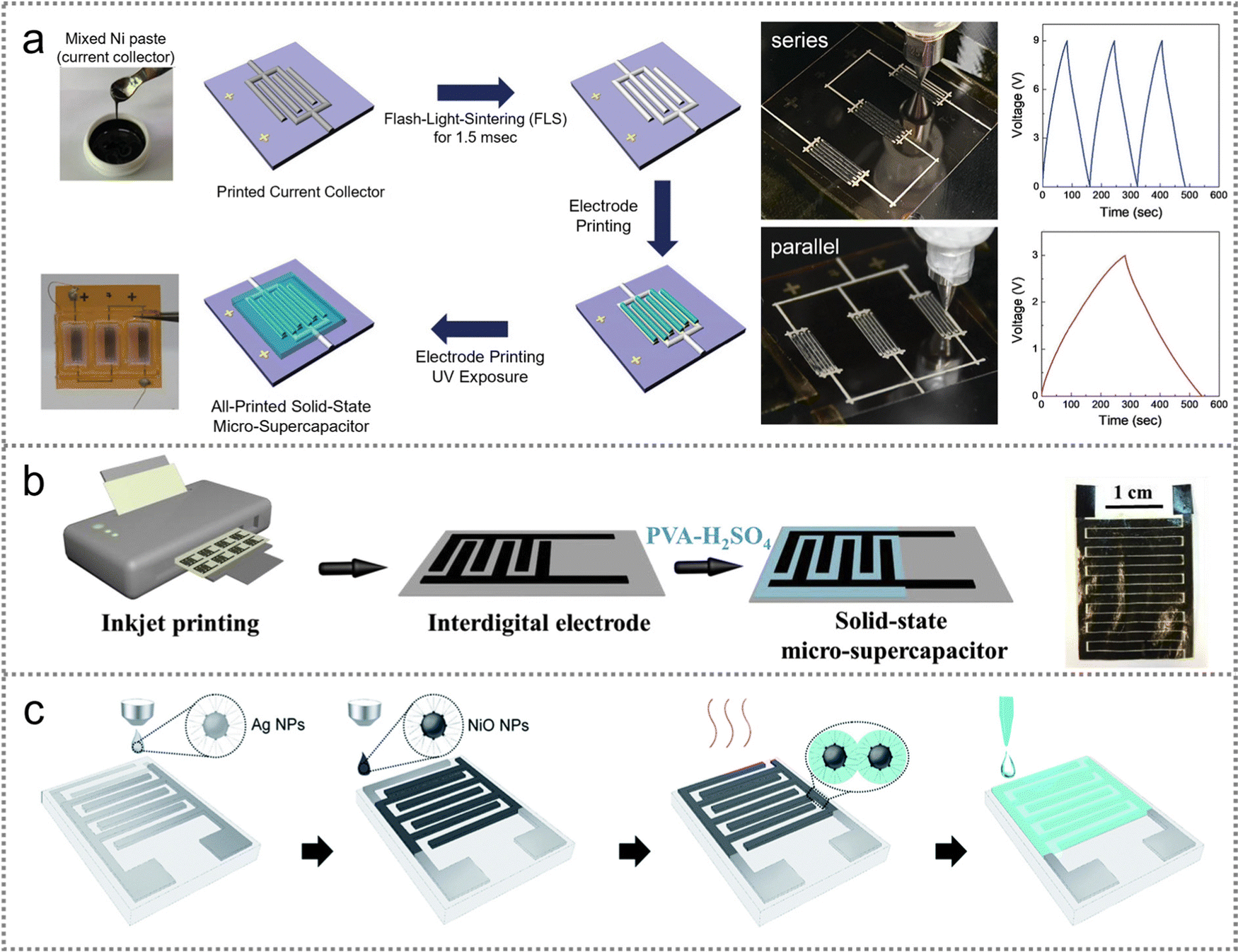 | ||
| Fig. 5 PMSC fabrication with the inkjet printing technique. (a) Schematic illustration of the sequential preparation process for the all-printed solid-state Ni S-MSC and a photograph of devices connected in series and parallel and the corresponding GCD curves. Reproduced with permission.70 Copyright 2020, Wiley-VCH. (b) Schematic illustrating the procedure of the fabrication for SA-MXene nanocomposite PMSCs and the photograph of an interdigital structure device. Reproduced with permission.71 Copyright 2019, Elsevier. (c) Schematic illustration of the fabrication process for inkjet-printed planar MSCs. Reproduced with permission.72 Copyright 2019, Royal Society of Chemistry. | ||
The current collector is critically needed on account of the poor conductivity of composite ink-state electrode materials. The single layer conductive substrate can ameliorate the inferior charge transfer between the bulk electrodes instead of mixing the active materials with binders and conductive components. Recently, a layer-by-layer printing strategy was developed to fabricate planar NiO MSCs by using the printed Ag nanoparticles (NPs) as the current collector (Fig. 5(c)).72 The conductivity of the film electrode was up to 210 S m−1. The adhesion between the Ag NPs and NiO NPs was enhanced by the sintering process to guarantee the high conductivity of the device.
In brief, the inkjet printing strategy can greatly shorten the manufacturing time for the scalable fabrication of PMSCs. But the remaining obstacle consists in the uncertain rheological characteristics of printing inks as well as the hydrophilicity of the substrates. The strong surface tension of inks and hydrophobic substrates may severely deteriorate the quality of printed electrodes. The size of ink drops is uncontrollable for designing a high-resolution micro electrode. Therefore, the forementioned bottlenecks require in-depth research on novel printing inks and substrates to ensure the scalable fabrication of printed PMSCs.
The laser scribing strategy is commonly used in combination with other techniques to fabricate high-quality PMSC devices. The fundamental procedures can be divided into two types.77,78 In the first type, the finger-structured current collectors are designed by the laser direct writing technique.79,80 The active materials can be loaded on conductive substrates via electrochemical deposition and mask-assisted coating methods. For example, a MnO2@polypyrrole(Ppy)@MWCNT asymmetric PMSC was developed by laser scribing and a successive electrodeposition process (Fig. 6(a)).81 In step I, six interdigital electrodes (0.5 mm × 5 mm) were designed through computer-controlled laser direct writing on an indium tin oxide-polyethylene terephthalate (ITO-PET) film. Then, the reduced graphene oxide (rGO) flakes were electrodeposited onto the interdigital ITO-PET substrate to serve as the current collector (step II). In the following steps, a Ppy@MWCNT cathode and MnO2 anode were anchored respectively on the patterned electrodes by an electrodeposition strategy. The asymmetric PMSC delivered a five-fold higher energy density of 12.16 μW h cm−2 at 5 mV s−1 than the symmetric PMSC (2.58 μW h cm−2). Commercial CNT paper could also be used as the raw material to construct PMSCs by laser engraving. The interdigital conductive substrate could be designed for further electrodeposition due to its superior conductivity (1–2 × 10⁵ S m−1) (Fig. 6(b)).82 The zinc ions were reduced and deposited onto the working electrode to serve as the anode of the zinc-ion micro-supercapacitor (ZmSC) by using the patterned CNTs as the working and counter electrode in 1 M ZnSO4 aqueous electrolyte. The entire manufacturing process was simple and efficient to ensure the replenishment of Zn without additional electrodes and electrolytes.
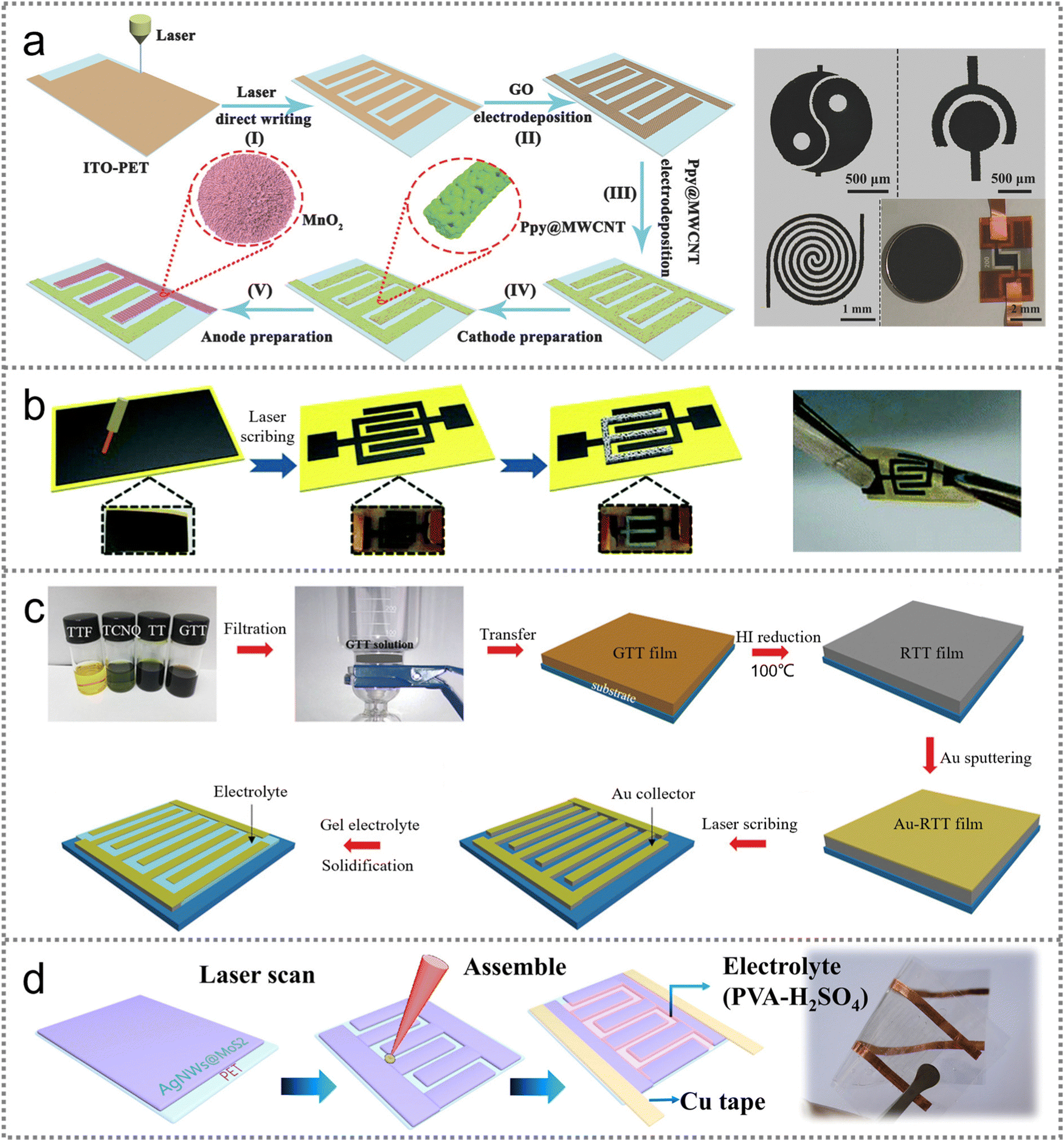 | ||
| Fig. 6 Laser scribing strategy for fabricating PMSCs. (a) Schematic illustration of the fabrication process for AMSC and digital photographs of electrodes with different shapes. Reproduced with permission.81 Copyright 2018, Wiley-VCH. (b) Schematic diagram of the preparation process for the ZmSC and corresponding photograph. Reproduced with permission.82 Copyright 2018, Royal Society of Chemistry. (c) Schematic illustrating the fabrication process of RTT-MSCs. Reproduced with permission.86 Copyright 2019, Wiley-VCH. (d) Direct laser-patterning technique for fabricating the TFE-TMSC. Reproduced with permission.87 Copyright 2018, Elsevier. | ||
In the second type, the film structured active material should be firstly prepared through spray coating and vacuum filtration strategies.83 The laser scribing technique can be used to tailor the film-shaped materials into a customized interdigital pattern.84,85 For example, the vacuum filtration method was conducted to fabricate graphene and tetrathiafulvalene-tetracyanoquinodimethane (GTT) based films for laser scribed reduced GTT (RTT) PMSCs (Fig. 6(c)).86 The obtained GTT film was transferred onto the PET substrate for the further reduction of GTT to RTT. After being covered with a 150 nm thick Au layer, the Au-RTT film was manufactured into finger structure electrodes by the laser scribing technique. Apart from the vacuum filtration method, the film-structured materials can also be prepared by a spray coating strategy. Recently, a spray coating combined with laser scribing strategy was developed to fabricate MoS2-based PMSCs on PET film (Fig. 6(d)).87 The Ag nanowires (AgNWs) were mixed with MoS2 in a water/ethanol solution to obtain a homogenous ink for spray coating, enabling the enhanced conductivity of the bulk electrode owing to the superior conductivity of the AgNWs. The interdigital pattern was designed on microelectrodes via a laser scribing process followed by coating PVA/H2SO4 gel electrolyte to assemble the PMSC device. Although the laser scribing strategy can directly fabricate microelectrodes without tedious procedures, the expensive equipment may restrict the widespread application in large-scale industrial production.
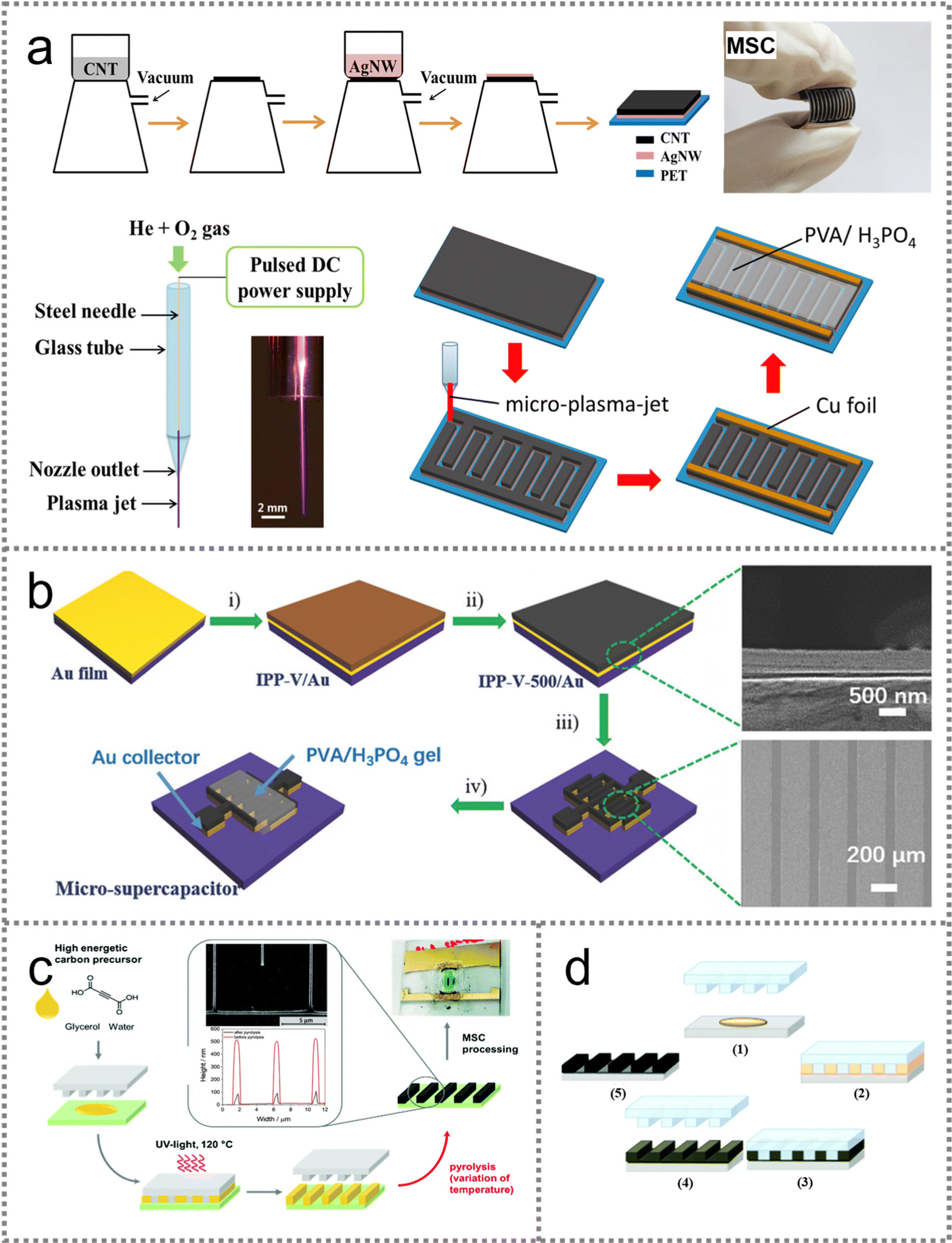 | ||
| Fig. 7 PMSC fabrication with plasma jet and nanoimprint lithography strategies. (a) Schematic illustration of the fabrication process of flexible in-plane MSCs and the configuration of the micro-plasma-jet setup. Reproduced with permission.89 Copyright 2018, IOP. (b) Schematic diagram of the construction procedure for the IPP-V-500 based MSC with plasma etching and the cross-sectional and top-view SEM images. Reproduced with permission.90 Copyright 2018, Wiley-VCH. (c) Solvent-assisted nanoimprint process for fabricating PMSCs. Reproduced with permission.92 Copyright 2021, Royal Society of Chemistry. (d) Schematic illustration of the preparation procedure for the printed interdigital electrodes. Reproduced with permission.93 Copyright 2018, Royal Society of Chemistry. | ||
![[thin space (1/6-em)]](https://www.rsc.org/images/entities/char_2009.gif) 000 cycles at 8.3 μA cm−2. In addition, sucrose-derived carbon was used as an EDLC type material to fabricate interdigital electrodes via the nanoimprint lithography technology (Fig. 7(d)).93 The width of the micro-structured fingers in the MSC could be further reduced to 500 nm. The interdigital carbon-based electrodes were peeled off from the stamps and the morphology remained intact after the pyrolysis process. Therefore, the nanoimprint lithography technique can be extensively used in the scalable production of micro- and nanoscale devices, indicating the feasibility of fabricating miniaturized electronic components.
000 cycles at 8.3 μA cm−2. In addition, sucrose-derived carbon was used as an EDLC type material to fabricate interdigital electrodes via the nanoimprint lithography technology (Fig. 7(d)).93 The width of the micro-structured fingers in the MSC could be further reduced to 500 nm. The interdigital carbon-based electrodes were peeled off from the stamps and the morphology remained intact after the pyrolysis process. Therefore, the nanoimprint lithography technique can be extensively used in the scalable production of micro- and nanoscale devices, indicating the feasibility of fabricating miniaturized electronic components.
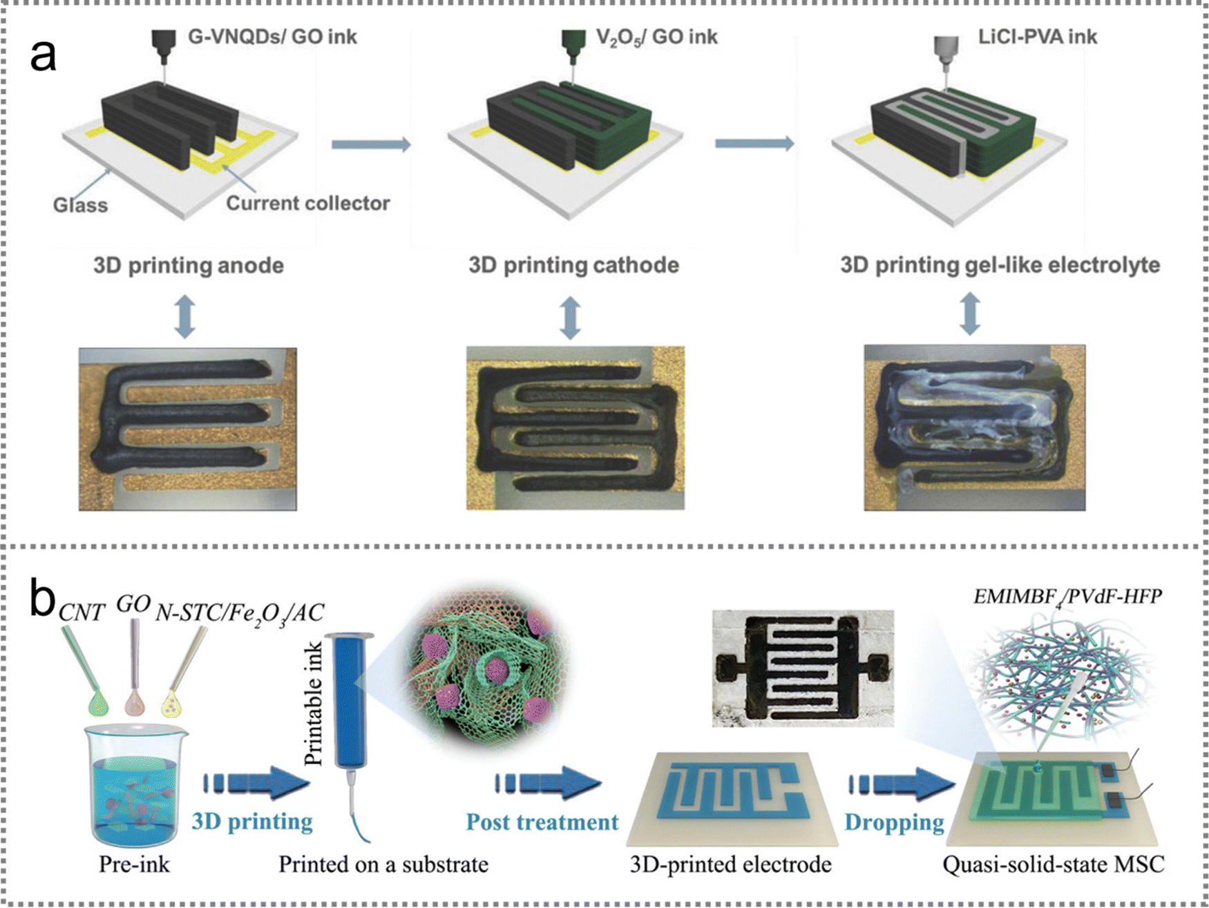 | ||
| Fig. 8 3D printing technology for the fabrication of PMSCs. (a) G-VNQDs/GO anode, V2O5/GO cathode and LiCl-PVA gel-like electrolyte constructed with the 3D printing method. Reproduced with permission.97 Copyright 2018, Wiley-VCH. (b) Schematic illustration of the ionogel-based quasi-solid-state MSC. Reproduced with permission.98 Copyright 2020, Wiley-VCH. | ||
Overall, the 3D printing technique has showcased practicability in designing on-chip microdevices. Microelectrodes with interdigital patterns can be accurately printed according to pre-designed configurations in computer programs. However, the active material printing ink should be developed with suitable shear-thinning rheological properties and fluidity. A high solid content is also required for printing inks to be extruded through nozzles without structural collapse. Hence, research on 3D printing techniques is still confronted with tremendous challenges for the manufacture of high-precision PMSCs.
In brief, PMSCs can be designed and manufactured through mask-assisted strategies and other advanced techniques. The devices fabricated with the above-mentioned microfabrication technologies are summarized in Table 1, considering the interdigital width, interspace and electrochemical performance. The vacuum filtration and spray coating strategy showed limitations in reducing the size of the microelectrode from millimeters to micrometers. With the assistance of advanced microfabrication machines, the interdigital width of PMSCs could even be reduced to 500 nm with the interspace of 1 μm by the nanoimprint lithography technique. However, the feasibility of each strategy depends on the structure of the raw materials, and it is still a crucial challenge to develop a facile technique for designing and manufacturing high performance PMSCs.
| Techniques | PMSCs | Interdigital width/mm | Interspace/mm | Substrate | Electrolyte | Potential window/V | C a/mF cm−2 | E max/mW h cm−3 | P max/W cm−3 | Cycling stability | Ref. |
|---|---|---|---|---|---|---|---|---|---|---|---|
| Vacuum filtration | CuHCF/graphene//FeHCF/graphene | 1.6 | 1.6 | PET | PVA/LiCl | 0–1.8 | 19.84 | 44.6 | 16.88 | 5000 (96.8%) | 48 |
| Ti3C2Tx/MnO2//Ti3C2Tx/MnO2 | 1 | — | PET | PVA/EMIMBF4 | 0–2.5 | 24.7 | 21.5 μW h cm−2 | 0.154 mW cm−2 | 3000 (83.6%) | 49 | |
| VN//MnO2 | 1 | 0.5 | Nylon membrane | SiO2-LiTFSI | 0–2.0 | 16.1 | 21.6 | 1.539 | 5000 (90%) | 50 | |
| g-C34N6-COF//g-C34N6-COF | 1.6 | 1.6 | PET | PVA/LiCl | 0–0.8 | 15.2 | 7.3 | 10 | 5000 (93.1%) | 53 | |
| Spray coating | NMCSs//NMCSs | 1 | 0.5 | PET | PVA/H2SO4 | 0–1 | 22.11 | 0.307 | 0.058 | — | 55 |
| PANI/C-MWCNTs//PANI/C-MWCNTs | 1 | 1 | PET | PVA/H2SO4 | 0–0.8 | 45.4 | 2.6 | 1.49 | 1000 (84.6%) | 56 | |
| LRGO@PANI//LRGO@PANI | 2 | 1 | PET | PVA/H2SO4 | −1.0 to 1.0 | 72.0 | 2.7 | — | 1000 (93.5%) | 57 | |
| CF-MnO//CF-Fe2O3 | 1 | 0.7 | Glass | PVA/KOH | 0–1.4 | 18.4 | 5 μW h cm−2 | 3440.7 μW cm−2 | 10000 (86.1%) | 58 | |
| rGO@PANI-NR//rGO@PANI-NR | 2 | 1 | PET | PVA/H2SO4 | −1.0 to 1.0 | 51 | 52.2 W h kg−1 | 3722.3 W kg−1 | 1000 (98.3%) | 59 | |
| Electrolytic deposition | Mn/V oxide@MWCNT//Mn/V oxide@MWCNT | — | — | PI | Polycarbonate/sulfolane/LiClO4/polymethylmethacrylate | 0–2 | 11.8 | 6.58 μW h cm−2 | 1.0 mW cm−2 | 5000 (78%) | 62 |
| Ti3C2Tx//V2O5 | 1.5 | 0.1 | PI | Polyacrylamide/ZnSO4 | 0–1.65 | 129 | 48.9 μW h cm−2 | — | 10000 (77%) | 63 | |
| Electrophoretic deposition | AC//AC | 0.5 | 0.3 | PI | 1 M KNO3 | 0–1.6 | 76.6 | 13.61 μW h cm−2 | 40.0 mW cm−2 | 5000 (92.9%) | 64 |
| Carbon//carbon/TiO2 | 0.6 | 0.15 | PI | PVA/H2SO4 | 0–1.0 | 27.3 | — | — | 10000 (100%) | 65 | |
| Inkjet printing | MWCNTs/graphene//MWCNTs/graphene | 0.25 | — | PI | EMIM-TFSI | 0–3.0 | 16.15 | 79 mJ cm−2 | 12.8 mW cm−2 | — | 70 |
| SA-MXene//SA-MXene | — | — | Photo paper | PVA/H2SO4 | 0–1.0 | 108.1 | 100.2 | — | 4000 (94.7%) | 71 | |
| NiO//NiO | 1 | 0.5 | PET | PVA/Mg(ClO4)2 | 0–1.0 | 155 | — | — | 5300 (94%) | 72 | |
| Laser scribing | MnO2//Ppy@MWCNT | 0.5 | 0.2 | ITO-PET | PVA/LiCl | 0–1.6 | 21.8 | 12.16 μW h cm−2 | — | — | 81 |
| Zn/CNT//CNT | 0.5 | 0.3 | PI | 1 M ZnSO4 | 0–1.8 | 83.2 | 29.6 μW h cm−2 | 8 mW cm−2 | 6000 (87.4%) | 82 | |
| RTT//RTT | 0.5 | 0.3 | PET | PVA/H2SO4 | 0–1.0 | 151 μF cm−2 | 1.57 | 0.2 | 10000 (98%) | 86 | |
| AgNWs-MoS2//AgNWs-MoS2 | 1 | 25 μm | PET | PVA/H2SO4 | 0–1.2 | 27.6 | 2.453 μW h cm−2 | — | 20000 (85.2%) | 87 | |
| Plasma jet | MWCNT/AgNW//MWCNT/AgNW | 0.8 | 0.2 | PET | PVA/H3PO4 | 0–0.8 | 274.8 μF cm−2 | 0.17 | — | 10000 (92.3%) | 89 |
| IPP-V-500//IPP-V-500 | 0.2 | 64 μm | Si wafer | PVA/H3PO4 | 0–1.0 | — | 0.35 | — | — | 90 | |
| Nanoimprint lithography | Carbon//carbon | 500 nm | 1 μm | B-Al silicate | PVA/H2SO4 | 0–0.8 | 1.32 | 0.07 | — | 10000 (97%) | 92 |
| N-doped carbon//N-doped carbon | 500 nm | 1 μm | Glass | PVA/H2SO4 | 0–1.0 | 65 μF cm−2 | 58 | 22 | 1000 (98%) | 93 | |
| 3D printing | G-VNQDs/GO//V2O5/GO | 0.2 | 0.3 | Glass | PVA/LiCl | 0–1.6 | 207.9 | 73.9 μW h cm−2 | — | 8000 (65%) | 97 |
| N-STC/Fe2O3//N-STC/Fe2O3 | 0.75 | 1.25 | PET | EMIMBF4/PVDF-HFP | 0–4.0 | 1.79 F cm−2 | 114 W h kg−1 | 0.1 kW kg−1 | 10000 (93.2%) | 98 |
4. Applications
PMSCs have exhibited a variety of advantages including high power densities, superior flexibility and excellent rate capability, showing great potential for integration into electronic components.98 As demonstrated in previous reports, the development of various micro-electronics has stimulated the miniaturization of energy storage systems. The configuration of PMSCs differs dramatically from conventional batteries and sandwich-structured SCs. The unique planar structure enables fast ion transport kinetics in the horizontal direction, which can contribute to the enhanced rate capability. The reduction in size allows the PMSC to be used as a novel energy storage device for microelectronics. Meanwhile, PMSCs can also be utilized in flexible power supplies and wearable sensors owing to their superior mechanical flexibility.99,100 With the characteristics of cutting off DC, connecting the alternating current (AC) and preventing low frequency, PMSC-based electric systems can be used as energy filters in power grids to compensate the intermittency of fluctuant input power. In this section, the applications of PMSCs in energy storage devices, sensors and filters are discussed for next generation microelectronics.4.1 Energy storage devices
The emerging PMSCs can meet the requirements of miniaturized energy storage devices with decent power density, high-rate capability, and an almost indefinite cycling stability. The unique planar configuration allows the micro-sized unit to be integrated into on-chip electronics in parallel and series connections. For instance, ten inkjet-printed NiO MSCs (IPNIO) were connected in parallel and series configurations, respectively (Fig. 9(a)).72 The parallel connected devices exhibited a ten-fold higher capacity than a single IPNIO under the voltage window of 1 V. Meanwhile, devices connected in series presented a higher potential of 10 V, indicating the integratability of PMSCs in energy storage devices. In addition, the PMSC could retain the initial capacitance under bending states due to the planar configuration and flexible substrates. The stretchable PMSC arrays were fabricated and four devices could be connected in series and parallel with satisfactory mechanical flexibility (Fig. 9(b)).79 The voltage of the series connected devices was four times higher than that of a single PMSC with 0.6 V. The devices connected in parallel showed an equal voltage window to the single device. The flexible measurements demonstrated the superior capacity retention of PMSC arrays with increasing elongation from 0% to 100%. Scalable fabrication could also be realized with a linear relationship between the number of PMSC arrays and the capacitance. These features manifested the integratable characteristics of PMSCs in flexible and integrated microelectronics.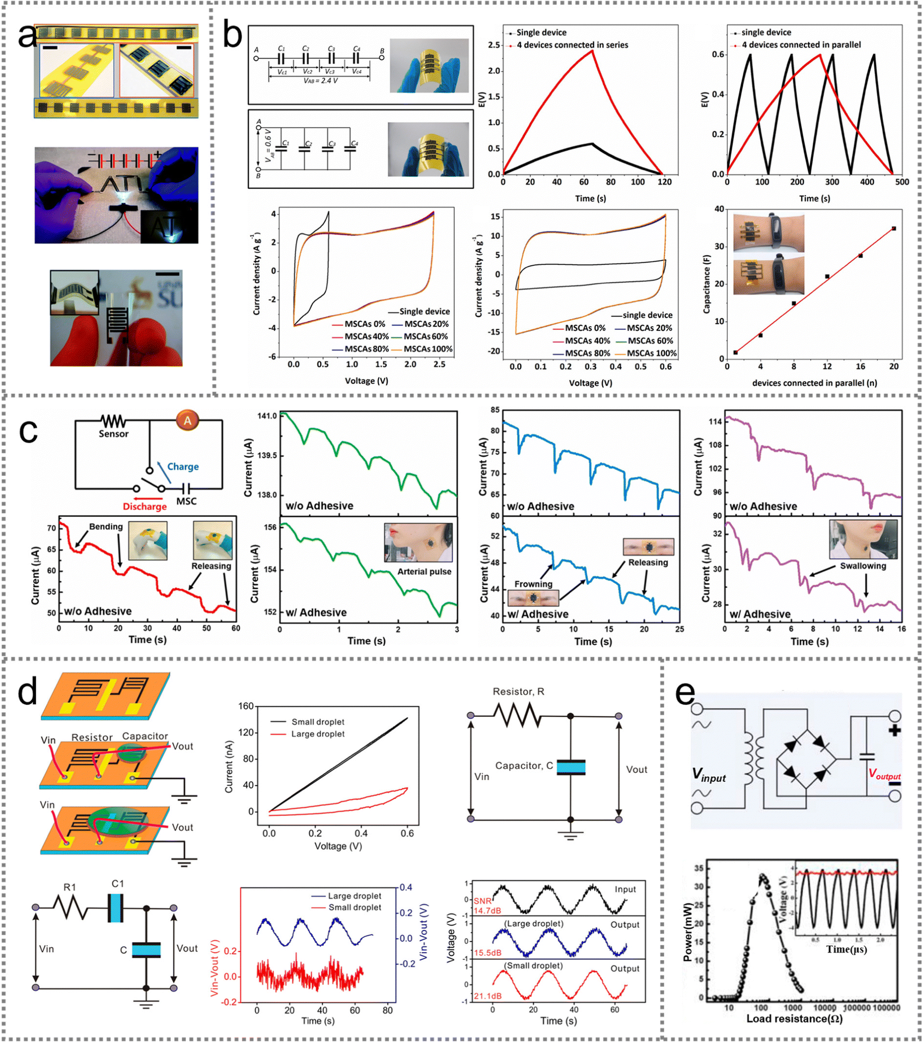 | ||
| Fig. 9 Applications of PMSCs including energy storage devices, sensors and filters. (a) Digital photographs of 10 IPNiO MSCs connected in parallel and series configurations, then used as the energy storage unit for LEDs. Reproduced with permission.72 Copyright 2019, Royal Society of Chemistry. (b) Electrochemical performance and flexibility of PMSCs with series and parallel connections. Reproduced with permission.79 Copyright 2021, Elsevier. (c) Schematic diagram of the integrated system and the strain measurement induced by bio-signals including arterial pulse, frowning and swallowing. Reproduced with permission.62 Copyright 2021, Elsevier. (d) The fsrGO MSCs applied in RC filter circuits. Reproduced with permission.101 Copyright 2018, American Chemical Society. (e) Schematic circuit diagram of the wireless charging unit and corresponding output power. Reproduced with permission.85 Copyright 2020, Elsevier. | ||
4.2 Sensors
PMSCs have been developed in bio-sensors to detect the strains induced by arterial pulse, respiration and body movements owing to their outstanding flexibility. The planar structure ensures that the device has a highly adhesive attachment onto the human skin. Recently, a skin-attachable bio-signal sensor was designed with a vertically integrated PMSC system to detect wrist bending, arterial pulse, frowning of the brow and swallowing signals (Fig. 9(c)).62 Adhesive film and PI tape were used in two contact modes to tightly attach the bio-sensor onto the skin for contact enhancement. The output electrochemical data suggested that the forementioned bio-signals could be evidently amplified by the PI attachment rather than the adhesive film. The sharper peaks in PI tape fixed sensors indicated the tighter adhesion between human skin and the bio-sensors, while the adhesive films might hamper the precise detection of bio-signal induced strains. Therefore, the adhesion mode remains an obstacle for PMSC-based planar sensors to accurately detect the bio-signals without skin irritation.4.3 Filters
High-quality power is critically needed in medical apparatus, signal processors and the communication industry. Filters are of great function for integrated grids to decrease the ripples and output a steady voltage. Similar to conventional SCs, PMSCs can also be used as resistor–capacitor (RC) filters to eliminate the interference signals. In particular, a graphene-based RC filter was assembled by using PMSCs and a fs laser reduced graphene oxide (fsrGO) resistor (Fig. 9(d)).101 The filters were divided into two types based on the size of the PVA/H2SO4 gel electrolyte droplet. In the first type, the interdigital microelectrode of the PMSC was precisely coated with a small electrolyte droplet, exhibiting a typical resistor feature with a linear loop in the current–voltage (CV) curve. Meanwhile, the filter coated with a large droplet showed a capacitive-type rectangular loop in the CV curve, leading to an increased number of capacitors in the equivalent circuit. When the sinusoidal signal at 0.045 Hz was applied with white noise, the small droplet-coated filter could output a stronger high-frequency noise with an increased signal-to-noise ratio (SNR) from 14.7 to 21.1 dB compared to that of the large droplet coated filter (15.5 dB). Therefore, the quality of the output signal could be affected by the coating domain of the gel electrolyte. Likewise, the series connected PMSC system was designed to convert the input AC voltage into the output DC voltage of 3.0 V (Fig. 9(e)).85 The wireless charging unit was assembled with the PMSC system for autonomous electronics, which delivered the maximum output power of 33.0 mW with an external load resistance of 60 Ω. Meanwhile, the voltage and power of the PMSC system were 3 V and 1.43 mW, demonstrating the feasibility of planar microdevices to be integrated into a self-powered system.5. Summary and outlook
In summary, the demand for miniaturized electronics has boosted the development of microelectrode designs and manufacturing strategies for PMSCs. The interdigital electrodes of PMSCs can be achieved by pre-designed masks in vacuum filtration and spray coating techniques for large-scale fabrication of millimeter-sized devices without time-consuming processes. The electrochemical strategies can further reduce the size of PMSCs and improve the resolution between the adjacent electrodes. Printing strategies and laser-induced techniques are also conducive to manufacturing micro- and nanoscale PMSCs with higher accuracy. Many challenges in the microfabrication techniques need to be conquered to pave the way for the realization of intelligent energy systems.The intrinsically inferior electrochemical performance of electrode materials hinders the energy and power density upper limit of PMSC devices. Novel EDLC-type and pseudocapacitive materials should be developed to compensate the performance deficiencies of PMSCs. In particular, composite electrodes can be designed by incorporating carbon-derived (EDLC type) and transitional metal-based materials (pseudocapacitive type) to maximize the synergistic effect. Meanwhile, the energy storage mechanisms should be elucidated in depth and the mass transfer dynamics at the electrode/electrolyte interface need to be probed for designing the expected electrode materials. Stable gel/solid-state electrolytes should be further exploited with an enticing potential window to improve the performance of PMSCs.
Advanced microfabrication technologies are needed to design high-resolution PMSCs on a grand scale. The distance between adjacent interdigital electrodes should be narrowed down to micrometers for a shortened ion diffusion pathway in plane. The finger-structure patterns are required to be loaded on a flexible and silicon substrate with tiny footprint areas. The affinity between the substrates and electrode materials should be further reinforced for long-term stability. A low contact resistance is desired to obtain efficient ion transport and charge transfer.
The monolithic integration of PMSCs into autonomous systems should be forged ahead for energy harvesters, sensors, filters and other untapped fields. We should further focus on miniaturized electronics with high flexibility and responsive capability. The requirement for micro power supplies in IoTs electronics pushes the incorporation of PMSCs into self-powered systems. So, various attempts should be unremittingly executed to break the bottlenecks for the development of PMSCs. Interdisciplinary cooperation is indispensable to guide the microelectronic systems towards a higher level.
Author contributions
Shifan Zhu: methodology, investigation, writing – original draft; Zhiheng Xu: methodology, validation, writing – review & editing; Haijun Tao: writing – review & editing, supervision; Dandan Yang: writing – review & editing; Xiaobin Tang: writing – review & editing, supervision; Yuqiao Wang: conceptualization, writing – review & editing, supervision, funding acquisition.Conflicts of interest
The authors declare that they have no known competing financial interests or personal relationships that could have appeared to influence the work reported in this paper.Acknowledgements
This work was financially supported by the Joint Funds of NUAA-SEU (6907046031) and Excellent Postdoctoral Program of Jiangsu Province (2022ZB235). We thank the Big Data Center of Southeast University for providing the facility support on the numerical calculations in this paper.References
- Y.-Z. Zhang, Y. Wang, T. Cheng, L.-Q. Yao, X. Li, W.-Y. Lai and W. Huang, Chem. Soc. Rev., 2019, 48, 3229–3264 RSC.
- B. D. Boruah, Energy Storage Mater., 2019, 21, 219–239 CrossRef.
- Q. Liu, G. Zhang, N. Chen, X. Feng, C. Wang, J. Wang, X. Jin and L. Qu, Adv. Funct. Mater., 2020, 30, 2002086 CrossRef CAS.
- X. Chen, N. S. Villa, Y. Zhuang, L. Chen, T. Wang, Z. Li and T. Kong, Adv. Energy Mater., 2020, 10, 1902769 CrossRef CAS.
- P. Zhang, S. Yang, H. Xie, Y. Li, F. Wang, M. Gao, K. Guo, R. Wang and X. Lu, ACS Nano, 2022, 16, 17593–17612 CrossRef CAS PubMed.
- Y. Jiang, J. Ou, Z. Luo, Y. Chen, Z. Wu, H. Wu, X. Fu, S. Luo and Y. Huang, Small, 2022, 2201377 CrossRef CAS PubMed.
- L. Chen, F. Wang, Z. Tian, H. Guo, C. Cai, Q. Wu, H. Du, K. Liu, Z. Hao, S. He, G. Duan and S. Jiang, Small, 2022, 2201307 CrossRef CAS PubMed.
- X. Shi, S. Zheng, Z.-S. Wu and X. Bao, J. Energy Chem., 2018, 27, 25–42 CrossRef.
- J. Wang, F. Li, F. Zhu and O. G. Schmidt, Small Methods, 2019, 3, 1800367 Search PubMed.
- Y.-Q. Li, H. Shi, S.-B. Wang, Y.-T. Zhou, Z. Wen, X.-Y. Lang and Q. Jiang, Nat. Commun., 2019, 10, 4292 CrossRef PubMed.
- M. Beidaghi and Y. Gogotsi, Energy Environ. Sci., 2014, 7, 867–884 RSC.
- R. Peri, S. Balasubramanian and M. Bhagavathiachari, J. Energy Storage, 2022, 50, 104636 CrossRef.
- C. Peng, Q. Li, L. Niu, H. Yuan, J. Xu, Q. Q. Yang, Y. J. Yang, G. Li and Y. Zhu, Carbon, 2021, 175, 27–35 CrossRef CAS.
- I. Karbhal, A. Basu, A. Patrike and M. V. Shelke, Carbon, 2021, 171, 750–757 CrossRef CAS.
- W. A. Haider, M. Tahir, L. He, H. A. Mirza, R. Zhu, Y. Han and L. Mai, ACS Cent. Sci., 2020, 6, 1901–1915 CrossRef CAS PubMed.
- N. A. Kyeremateng, T. Brousse and D. Pech, Nat. Nanotechnol., 2017, 12, 7–15 CrossRef CAS PubMed.
- C. Gao, J. Huang, Y. Xiao, G. Zhang, C. Dai, Z. Li, Y. Zhao, L. Jiang and L. Qu, Nat. Commun., 2021, 12, 2647 CrossRef CAS PubMed.
- J. Zhang, G. Zhang, T. Zhou and S. Sun, Adv. Funct. Mater., 2020, 30, 1910000 CrossRef CAS.
- F. Bu, W. Zhou, Y. Xu, Y. Du, C. Guan and W. Huang, npj Flexible Electron., 2020, 4, 31 CrossRef.
- P. Zhang, F. Wang, S. Yang, G. Wang, M. Yu and X. Feng, Energy Storage Mater., 2020, 28, 160–187 CrossRef.
- X. Zhang, W. Zhao, L. Wei, Y. Jin, J. Hou, X. Wang and X. Guo, Energy, 2019, 170, 338–348 CrossRef CAS.
- Y. Rong, Y. Chen, J. Zheng, Y. Zhao and Q. Li, J. Colloid Interface Sci., 2021, 598, 1–13 CrossRef CAS PubMed.
- T. Wang, H. C. Chen, F. Yu, X. S. Zhao and H. Wang, Energy Storage Mater., 2019, 16, 545–573 CrossRef.
- C. Wang, K. Xia, H. Wang, X. Liang, Z. Yin and Y. Zhang, Adv. Mater., 2019, 31, 1801072 CrossRef PubMed.
- X. Sun, K. Chen, F. Liang, C. Zhi and D. Xue, Front. Chem., 2022, 9, 807500 CrossRef PubMed.
- Y. Jiang and J. Liu, Energy Environ. Mater., 2019, 2, 30–37 CrossRef.
- C. Gao, K. Chen, Y. Wang, Y. Zhao and L. Qu, ChemSusChem, 2020, 13, 1255–1274 CrossRef CAS PubMed.
- X. Zhou, W. Long, Q. Wang, X. Dong and S. Tang, Adv. Mater. Interfaces, 2022, 9, 2200590 CrossRef CAS.
- J. Ma, J. Xia, Z. Liang, X. Chen, Y. Du and C.-H. Yan, Small, 2021, 17, 2104423 CrossRef CAS PubMed.
- T. Kim, S. Subedi, B. Dahal, K. Chhetri, T. Mukhiya, A. Muthurasu, J. Gautam, P. C. Lohani, D. Acharya, I. Pathak, S.-H. Chae, T. H. Ko and H. Y. Kim, Adv. Sci., 2022, 2200650 CrossRef CAS PubMed.
- M. Dai, D. Zhao and X. Wu, Chin. Chem. Lett., 2020, 31, 2177–2188 CrossRef CAS.
- C. Lethien, J. L. Bideau and T. Brousse, Energy Environ. Sci., 2019, 12, 96–115 RSC.
- J. Qin, J. Gao, X. Shi, J. Chang, Y. Dong, S. Zheng, X. Wang, L. Feng and Z.-S. Wu, Adv. Funct. Mater., 2020, 30, 1909756 CrossRef CAS.
- G. Lee, J. W. Kim, H. Park, J. Y. Lee, H. Lee, C. Song, S. W. Jin, K. Keum, C.-H. Lee and J. S. Ha, ACS Nano, 2019, 13, 855–866 CrossRef CAS PubMed.
- S. Jiang, X. Zhou, H. Xiao, W. Chen, X. Xu and Z. Liu, Chem. Eng. J., 2021, 405, 127009 CrossRef CAS.
- S. Selvam and J.-H. Yim, J. Mater. Chem. A, 2021, 9, 14319–14330 RSC.
- J. Yan, L. Miao, H. Duan, D. Zhu, Y. Lv, L. Li, L. Gan and M. Liu, Chin. Chem. Lett., 2022, 33, 2681–2686 CrossRef CAS.
- D. Jhajhria, P. Tiwari and R. Chandra, ACS Appl. Mater. Interfaces, 2022, 14, 26162–26170 CrossRef CAS PubMed.
- I. Khakpour, A. R. Baboukani, S. Forouzanfar, A. Allagui and C. Wang, J. Power Sources, 2021, 516, 230701 CrossRef CAS.
- S. Jiao, A. Zhou, M. Wu and H. Hu, Adv. Sci., 2019, 6, 1900529 CrossRef PubMed.
- N. Lin, H. Chen, W. Wang and L. Lu, Adv. Mater. Technol., 2021, 6, 2000991 CrossRef CAS.
- P. Das, X. Shi, Q. Fu and Z.-S. Wu, Adv. Funct. Mater., 2020, 30, 1908758 CrossRef CAS.
- L. Lu, D. Zhang, Y. Xie and W. Wang, J. Energy Storage, 2022, 51, 104458 CrossRef.
- A. Muzaffar, M. B. Ahamed, K. Deshmukh and J. Thirumalai, Renewable Sustainable Energy Rev., 2019, 101, 123–145 CrossRef CAS.
- J.-C. Li, J. Gong, X. Zhang, L. Lu, F. Liu, Z. Dai, Q. Wang, X. Hong, H. Pang and M. Han, ACS Appl. Energy Mater., 2020, 3, 3692–3703 CrossRef CAS.
- C. Zhao, Y. Liu, S. Beirne, J. Razal and J. Chen, Adv. Mater. Technol., 2018, 3, 1800028 CrossRef.
- R. Wang, S. Luo, C. Xiao, Z. Chen, H. Li, M. Asif, V. Chan, K. Liao and Y. Sun, Electrochim. Acta, 2021, 386, 138420 CrossRef CAS.
- Y. He, P. Zhang, M. Wang, F. Wang, D. Tan, Y. Li, X. Zhuang, F. Zhang and X. Feng, Mater. Horiz., 2019, 6, 1041–1049 RSC.
- X. Feng, J. Ning, M. Xia, H. Guo, Y. Zhou, D. Wang, J. Zhang and Y. Hao, Nanotechnology, 2021, 32, 035402 CrossRef CAS PubMed.
- J. Qin, S. Wang, F. Zhou, P. Das, S. Zheng, C. Sun, X. Bao and Z.-S. Wu, Energy Storage Mater., 2019, 18, 397–404 CrossRef.
- G. Ping, L. Miao, A. Awati, X. Qian, T. Shi, Y. Lv, Y. Liu, L. Gan, M. Liu and D. Zhu, Chin. Chem. Lett., 2021, 32, 3811–3816 CrossRef CAS.
- X. Zhang, G. Qu, Z. Wang, G. Xiang, S. Hao, X. Wang, X. Xu, W. Ma and G. Zhao, Chin. Chem. Lett., 2021, 32, 2453–2458 CrossRef CAS.
- J. Xu, Y. He, S. Bi, M. Wang, P. Yang, D. Wu, J. Wang and F. Zhang, Angew. Chem., Int. Ed., 2019, 58, 12065–12069 CrossRef CAS PubMed.
- C. Couly, M. Alhabeb, K. L. Van Aken, N. Kurra, L. Gomes, A. M. Nanarro-Suárez, B. Anasori., H. N. Alshareef and Y. Gogotsi, Adv. Electron. Mater., 2018, 4, 1700339 CrossRef.
- Y. Qiu, M. Hou, J. Gao, H. Zhai, H. Liu, M. Jin, X. Liu and L. Lai, Small, 2019, 15, 1903836 CrossRef CAS PubMed.
- X. Chu, Z. Zhu, H. Huang, Y. Xie, Z. Xu, Y. Wang, C. Yan, L. Jin, Y. Wang, H. Zhang and W. Yang, J. Power Sources, 2021, 513, 230555 CrossRef CAS.
- K. G. Laelabadi, R. Moradian and I. Manouchehri, ACS Appl. Energy Mater., 2020, 3, 5301–5312 CrossRef.
- S. Kumar and A. Misra, Nanoscale, 2021, 13, 19453–19465 RSC.
- K. G. Laelabadi, R. Moradian and I. Manouchehri, ACS Appl. Energy Mater., 2021, 4, 6697–6710 CrossRef.
- J. Lee, J. Y. Seok, S. Son, M. Yang and B. Kang, J. Mater. Chem. A, 2017, 5, 24585–24593 RSC.
- T. Purkait, G. Singh, N. Kamboj, M. Das and R. S. Dey, J. Mater. Chem. A, 2018, 6, 22858–22869 RSC.
- H. Park, C. Song, S. W. Jin, H. Lee, K. Keum, Y. H. Lee, G. Lee, Y. R. Jeong and J. S. Ha, Nano Energy, 2021, 83, 105837 CrossRef CAS.
- X. Li, Y. Ma, Y. Yue, G. Li, C. Zhang, M. Cao, Y. Xiong, J. Zou, Y. Zhou and Y. Gao, Chem. Eng. J., 2022, 428, 130965 CrossRef CAS.
- C. Huang, L. Kang, N. Zhang, S. Wan, X. Zhou and J. Zhang, ACS Appl. Mater. Interfaces, 2019, 11, 38303–38312 CrossRef CAS PubMed.
- J. Cai, C. Lv and A. Watanabe, RSC Adv., 2017, 7, 415–422 RSC.
- Y. Bräuniger, S. Lochmann, J. Grothe, M. Hantusch and S. Kaskel, ACS Appl. Energy Mater., 2021, 4, 1560–1567 CrossRef.
- H. J. Yang, J.-W. Lee, S. H. Seo, B. Jeong, B. Lee, W. J. Do, J. H. Kim, J. Y. Cho, A. Jo, H. J. Jeong, S. Y. Jeong, G.-H. Kim, G.-W. Lee, Y.-E. Shin, H. Ko, J. T. Han and J. H. Park, Nano Energy, 2021, 86, 106083 CrossRef CAS.
- Y. Lin, Y. Gao and Z. Fan, Adv. Mater., 2017, 29, 1701736 CrossRef PubMed.
- H. Chen, S. Chen, Y. Zhang, H. Ren, X. Hu and Y. Bai, ACS Appl. Mater. Interfaces, 2020, 12, 56319–56329 CrossRef CAS PubMed.
- C. Chae, J. H. Han, S. S. Lee, Y. Choi, T.-H. Kim and S. Jeong, Adv. Funct. Mater., 2020, 30, 2000715 CrossRef CAS.
- C.-W. Wu, B. Unnikrishnan, I.-W. P. Chen, S. G. Harroun, H.-T. Chang and C.-C. Huang, Energy Storage Mater., 2020, 25, 563–571 CrossRef.
- P. Giannakou, M. G. Masteghin, R. C. T. Slade, S. J. Hinder and M. Shkunov, J. Mater. Chem. A, 2019, 7, 21496–21506 RSC.
- H. Liu, Z. Sun, Y. Chen, W. Zhang, X. Chen and C.-P. Wong, ACS Nano, 2022, 16, 10088–10129 CrossRef CAS PubMed.
- J. Lin, Z. Peng, Y. Liu, F. R. Zepeda, R. Ye, E. L. G. Samuel, M. J. Yacaman, B. I. Yakobson and J. M. Tour, Nat. Commun., 2014, 5, 5714 CrossRef CAS PubMed.
- S. Kwon, Y. Yoon, J. Ahn, H. Lim, G. Kim, J.-H. Kim, K.-B. Choi and J. Lee, Carbon, 2018, 137, 136–145 CrossRef CAS.
- T. R. Anthony, J. Appl. Phys., 1982, 53, 9154–9164 CrossRef CAS.
- W. Yan, H. Hu, L. Wang and D. Ho, Small Methods, 2022, 2101616 CrossRef CAS PubMed.
- X.-Y. Fu, Z.-D. Chen, Y.-L. Zhang, D.-D. Han, J.-N. Ma, W. Wang, Z.-R. Zhang, H. Xia and H.-B. Sun, Nanoscale, 2019, 11, 9133–9140 RSC.
- C. Zhang, Z. Peng, C. Huang, B. Zhang, C. Xing, H. Chen, H. Cheng, J. Wang and S. Tang, Nano Energy, 2021, 81, 105609 CrossRef CAS.
- Y. Shao, J. Li, Y. Li, H. Wang, Q. Zhang and R. B. Kaner, Mater. Horiz., 2017, 4, 1145–1150 RSC.
- J. Gao, C. Shao, S. Shao, F. Wan, C. Gao, Y. Zhao, L. Jiang and L. Qu, Small, 2018, 14, 1801809 CrossRef PubMed.
- G. Sun, H. Yang, G. Zhang, J. Gao, X. Jin, Y. Zhao, L. Jiang and L. Qu, Energy Environ. Sci., 2018, 11, 3367–3374 RSC.
- B. Xie, Y. Wang, W. Lai, W. Lin, Z. Lin, Z. Zhang, P. Zou, Y. Xu, S. Zhou, C. Yang, F. Kang and C.-P. Wong, Nano Energy, 2016, 26, 276–285 CrossRef CAS.
- Y. Yuan, L. Jiang, X. Li, P. Zuo, C. Xu, M. Tian, X. Zhang, S. Wang, B. Lu, C. Shao, B. Zhao, J. Zhang, L. Qu and T. Cui, Nat. Commun., 2020, 11, 6185 CrossRef CAS PubMed.
- Y. Wu, H. Hu, C. Yuan, J. Song and M. Wu, Nano Energy, 2020, 74, 104812 CrossRef CAS.
- D. Zhao, W. Chang, C. Lu, C. Yang, K. Jiang, X. Chang, H. Lin, F. Zhang, S. Han, Z. Hou and X. Zhuang, Small, 2019, 15, 1901494 CrossRef CAS PubMed.
- J. Li, Q. Shi, Y. Shao, C. Hou, Y. Li, Q. Zhang and H. Wang, Energy Storage Mater., 2019, 16, 212–219 CrossRef.
- B. Dousti, S. Babu, N. Geramifard, M. Y. Choi, J. B. Lee, S. F. Cogan and G. S. Lee, J. Power Sources, 2022, 520, 230779 CrossRef CAS.
- L. Liu, H. Y. Li, Y. Yu, L. Liu and Y. Wu, Nanotechnology, 2018, 29, 055401 CrossRef PubMed.
- L. Wang, J. Ding, S. Sun, B. Zhang, X. Tian, J. Zhu, S. Song, B. Liu, X. Zhuang and Y. Che, Adv. Mater. Interfaces, 2018, 5, 1701679 CrossRef.
- C. Gao, J. Gao, C. Shao, Y. Xiao, Y. Zhao and L. Qu, J. Mater. Chem. A, 2018, 6, 19750–19756 RSC.
- C. Gellrich, S. Lochmann, T. Otto, J. Grothe and S. Kaskel, Mater. Adv., 2021, 2, 6380–6387 RSC.
- S. Lochmann, J. Grothe, K. Eckhardt, D. Leistenschneider, L. Borchardt and S. Kaskel, Nanoscale, 2018, 10, 10109–10115 RSC.
- Z. Wang, Q. E. Zhang, S. Long, Y. Luo, P. Yu, Z. Tan, J. Bai, B. Qu, Y. Yang, J. Shi, H. Zhou, Z.-Y. Xiao, W. Hong and H. Bai, ACS Appl. Mater. Interfaces, 2018, 10, 10437–10444 CrossRef CAS PubMed.
- Y. Zhang, T. Ji, S. Hou, L. Zhang, Y. Shi, J. Zhao and X. Xu, J. Power Sources, 2018, 403, 109–117 CrossRef CAS.
- X. Li, S. Ling, W. Cao, L. Zeng, R. Yuan and C. Zhang, Angew. Chem., Int. Ed., 2022, 61, 202202663 Search PubMed.
- K. Shen, J. Ding and S. Yang, Adv. Energy Mater., 2018, 8, 1800408 CrossRef.
- F. Lai, C. Yang, R. Lian, K. Chu, J. Qin, W. Zong, D. Rao, J. Hofkens, X. Lu and T. Liu, Adv. Mater., 2020, 32, 2002474 CrossRef CAS PubMed.
- C. Gao, C. Bai, J. Gao, Y. Xiao, Y. Han, A. Shaista, Y. Zhao and L. Qu, J. Mater. Chem. A, 2020, 8, 4055–4061 RSC.
- Z. Liu, H. I. Wang, A. Narita, Q. Chen, Z. Mics, D. Turchinovich, M. Klaui, M. Bonn and K. Müllen, J. Am. Chem. Soc., 2017, 139, 9443–9446 CrossRef CAS PubMed.
- D. Shen, G. Zou, L. Liu, W. Zhao, A. Wu, W. W. Duley and Y. N. Zhou, ACS Appl. Mater. Interfaces, 2018, 10, 5404–5412 CrossRef CAS PubMed.
Footnote |
| † These authors contributed equally to this work. |
| This journal is © The Royal Society of Chemistry 2023 |