
Bifunctional solid state electrochromic device using WO3/WS2 nanoflakes for charge storage and dual-band color modulation†
Suchita
Kandpal
a,
Love
Bansal
a,
Anjali
Ghanghass
b,
Tanushree
Ghosh
a,
Chanchal
Rani‡
a,
Bhumika
Sahu
a,
Deb Kumar
Rath
a,
Ravi
Bhatia
b,
I.
Sameera
 *b and
Rajesh
Kumar
*ac
*b and
Rajesh
Kumar
*ac
aMaterials and Device Laboratory, Department of Physics, Indian Institute of Technology Indore, Simrol-453552, India. E-mail: rajeshkumar@iiti.ac.in
bDepartment of Physics, Guru Jambheshwar University of Science & Technology, Hisar, 125001, India
cCentre for Advanced Electronics, Indian Institute of Technology Indore, Simrol-453552, India
First published on 14th August 2023
Abstract
A new methodology to enhance electrochromic performance and make it multifunctional ready has been demonstrated where an all-organic solid state electrochromic device has been made to display dual band color switching in the visible and near-infrared (NIR) spectrum. Additionally, energy storage capabilities have been added to make it a multifunctional solid-state device. A mixture of WS2/WO3 synthesized by the hydrothermal technique was characterized by X-ray diffraction, scanning electron microscopy (SEM), and Raman microscopy, prior to being used as a dopant with polythiophene (P3HT) and ethyl viologen (EV) active electrochromic layers. In situ kinematics was performed to check the electrochromic performance of the device in two wavelength (visible ∼515 nm and NIR ∼800 nm) regions. The fabricated device shows improved electrochromic performance in terms of switching time, color contrast, efficiency, and stability/cyclability in both wavelength regions of the electromagnetic spectrum. A very small external voltage bias (±1.5 V) was enough to switch the device (magenta ↔ blue) very quickly by taking less than a second's time. Furthermore, the supercapacitive performance parameters of the device have been investigated through cyclic voltammetry (CV), galvanostatic charge/discharge (GCD) curves, and electrochemical impedance spectroscopy (EIS). The results show that the specific capacitance value of the device is ∼50 F g−1 at a current density of 1 A g−1 along with a fast response (charging/discharging) time and excellent energy density. The designed electrochromic supercapacitor device successfully demonstrated excellent capacitive performance along with ability as an electrochromic indicator and paves the way for the integration of electrochromic energy storage indicators in various energy storage or energy-efficient buildings.
1. Introduction
Smart electrochromic devices (ECDs),1–4 which can control transmittance light through small applied voltages are becoming preferred choices for use in electrochromic smart windows/displays that can regulate the amount of light entering a building.5 In addition to the inherent color changing applications, recently, the functionalities of these devices have been extended by adding energy storage technology, which is referred to as electrochromic supercapacitors (ESCs).6–8 The research on dual-functioning electrochromic devices is increasing because these devices not only change their optical properties (color or transparency) but also store energy by the applied external voltage. Moreover, solar radiation transmittance can also be modulated by electrochromic windows to control the temperature of the ambience, which is very promising for designing energy efficient buildings.9–12 This application is more helpful if the device displays color modulation in the infrared (IR) region, which actually is the major component that causes heating. In other words, an electrochromic device with dual band color switching and added supercapacitive capabilities will be a technologically advantageous device to demonstrate. Therefore, incorporating smart materials in devices is highly desirable for multiple applications that can easily allow estimating or determining the storage of electrical energy, which is of great significance. Materials showing overlapping properties between electrochromic and supercapacitive nature may be a great choice to design such multifunctional devices.It is well-known that the electrode material plays a vital role to achieve high-performance ESCs, which contain a series of active electrodes including metal oxides/dichalcogenides, carbon-based materials, MOFs, conducting polymers, and their composites.13–23 Some transition metal oxides or conducting polymers such as polythiophene, polyaniline, WO3, V2O5, MnO2, etc. are widely used active materials for both electrochromic and energy storage applications due to their faradic reactions between the active material and electrolyte.24,25 However, a large proportion of CPs have poor cycling stability, but polythiophene (P3HT)26,27 is one of the most favorable materials in the field of electrochromic and energy storage due to its high conductivity, good thermal properties, and long-term stability. Though the value of its capacitance is not much, it can potentially be enhanced by doping with 2D materials, capable of offering a large surface area, more electroactive sites, and faster ion transport properties. Despite offering all these merits, the transition metal dichalcogenides (TMDs) still suffer from poor cycle life due to the restacking of the nanolayers. The poor structural integrity can be resolved by developing composites or mixtures, or developing hybrid core/shell nanostructures.28–31 Among the TMDs, WS2 with a covalently bonded S–W–S layered structure offers a large surface area, making it one of the ideal energy storage materials, but on the other side, its inherent color decreases the electrochromic color contrast.32–35 Thus, nanoflakes of WS2/WO3 might be a good option to opt for as a dopant to make a device suitable for electrochromic as well as energy storage applications without compromising the electrochromic performance of the device. Using the WS2/WO3 combination as a dopant, in a device fabricated using well-established electrochromic materials, instead of the main active layer, could be a better choice as they will help in managing the redox activity without hindering the electrochromic operation as has been investigated here.
In the current work, a mixture of WS2/WO3 was synthesized, by a hydrothermal technique, for utilization in fabricating a multifunctional P3HT/EV-based electrochromic charge storage device. In situ bias-dependent UV-Vis spectroscopy and electrochemical measurements show a fast switching between magenta and blue states with a small bias of 1.5 V. Compared with the undoped polythiophene-based devices, the fabricated device has outstanding electrochromic/supercapacitor properties in terms of a large contrast ratio of ∼52%, fast switching speeds (0.5 s/0.7 s at λ ∼ 515 nm and 0.8 s/0.8 s at λ ∼ 800 nm), excellent coloration efficiency and high specific capacitance along with charging/discharging stability under fast switching conditions. The successfully fabricated multifunctional solid-state device displays a change in color under small external bias and stores the energy supplied for coloration making it a multifunctional energy-storing ECSD with great potential for use in the next-generation smart electrochemical components. The multifunctional solid state ECD, in addition to the above-mentioned dual application in energy storage & electrochromic color change, displays color modulation in two bands vis-e-vis visible as well as near infrared. The latter may give an additional advantage in designing thermal control smart windows to be used in next-generation smart electrochemical components.
2. Experimental details
2.1 Chemicals used
Commercial grade chemicals, polyethylene oxide (PEO, Alfa Aesar, MW = 100![[thin space (1/6-em)]](https://www.rsc.org/images/entities/char_2009.gif) 000), ethyl viologen diperchlorate (EV, 98%, Sigma Aldrich), poly(3-hexyl thiophene-2,5-diyl) (P3HT, regioregular, Sigma Aldrich), ammonium paratungstate, thiourea, 1,2-dichlorobenzene (DCB, anhydrous, 99%, Sigma Aldrich) and acetonitrile (ACN, anhydrous, 99%, Sigma Aldrich) were used for device fabrication in the present study.
000), ethyl viologen diperchlorate (EV, 98%, Sigma Aldrich), poly(3-hexyl thiophene-2,5-diyl) (P3HT, regioregular, Sigma Aldrich), ammonium paratungstate, thiourea, 1,2-dichlorobenzene (DCB, anhydrous, 99%, Sigma Aldrich) and acetonitrile (ACN, anhydrous, 99%, Sigma Aldrich) were used for device fabrication in the present study.
2.2 WS2/WO3 synthesis
A facile one-step hydrothermal method was used for the synthesis of WS2/WO3 nanoflakes. The synthesis was performed using 1:3 weight ratio of ammonium paratungstate [(NH4)10(H2W12O42)·4H2O] and thiourea [(NH2)2CS]. The precursors were dissolved in 70 mL of de-ionized water by continuous stirring for 30 minutes. A homogeneous and colorless solution was obtained after stirring. The solution was transferred into a 100 mL Teflon-lined stainless steel hydrothermal reactor. The reactor was heated to 240 °C in a muffle furnace for 3 h and then allowed to cool down to room temperature. The nanoflake sample in the form of a greyish black precipitate was collected after centrifugation and then washed with de-ionized water and ethanol several times. The reaction product was dried overnight using a vacuum oven at 60 °C.36,37
2.3 Device fabrication
For the fabrication of the electrochromic device (ECD), thin films of P3HT and WS2/WO3 doped ethyl viologen, grown through the spin coating and drop casting techniques over ITO-coated glass substrates, have been used. For this, three different solutions i.e., 0.3 wt% P3HT in DCB, 5 wt% PEO in ACN and 4 wt% EV in ACN were prepared by using vortex mixing. The P3HT film (∼1 μm thick) was spin-coated on an ITO-coated glass substrate at 500 rpm for 120 s and then annealed at 80 °C for one hour, whereas a layer of EV (premixed with WS2/WO3) in a PEO matrix was drop casted on another ITO coated glass substrate and then assembled together with the help of double-sided tape using the simple flip-chip method as reported elsewhere in detail.382.4 Characterization and measurements
Structural and morphological characterizations of the synthesized nanoflakes have been carried out by using a Rigaku Smart lab Multipurpose Versatile XRD and 7610F Plus/JEOL field emission scanning electron microscope (FESEM). Raman spectra were recorded at a wavelength of 532 nm by using an Alpha300/WITec Raman spectrometer. Electrochemical measurements of the device have been done using a Keithley-2450 workstation and a Metrohm-Multi Autolab M204 potentiostat. The PerkinElmer make lambda 365 spectrometer was used for all in situ bias-dependent UV-Vis measurements.3. Results and discussion
Prior to making an electrochromic energy storage device, hydrothermally synthesized WS2/WO3 nanoflakes have been characterized by SEM, XRD and Raman spectroscopy.The FESEM micrograph (Fig. 1(a)) depicts the morphological aspect of the hydrothermally synthesized WS2/WO3 nanoflakes. It can be clearly observed that the synthesized nanoflakes have a thickness in the range of ∼10 nm. The EDS measurements (Fig. S1, ESI†) reveal the presence of W, O and S in the sample, which confirms the nanoflakes of WS2/WO3. The structural characteristics were analyzed using XRD data (Fig. 1(b)). The diffraction peaks at ∼ 13.7°, 28.7°, 31.3°, 39.0°, 43.0°, 49.47°, 59.3°, 65.4° and 75.8° correspond to the (002), (004), (101), (103), (006), (105), (112), (114) and (205) planes of the 2H-phase of WS2 [JCPDS card no: 08-1398] and the peaks at 24.0°, 27.7°, 34.0°, 36.9°, 42.1°, 47.1°, 54.0° and 57.7° correspond to the (001), (200), (111), (201), (300), (002), (221) and (400) planes of the hexagonal phase of WO3 [JCPDS card no: 75-2187].39,40 The peak marked by an asterisk (*) represents the (111) plane of orthorhombic WO3.0.33H2O.41 The structural features of the nanoflake sample have been further verified using Raman spectroscopy (inset, Fig. 1(b)). The peaks centered at ∼351.5 and 420.5 cm−1 are attributed to the E12g and A1g modes of WS2.42 The E12g mode is associated with the interlayer atomic vibrations of the W–S bond with both the atoms moving in opposite directions, whereas the A1g mode is related to the intralayer vibrations of S atoms. The peaks at ∼173 and 269 cm−1 represent the bending (W–O–W) mode of the bridging oxygen, whereas the peak at ∼788 cm−1 corresponds to the stretching (O–W–O) vibrational mode of tungsten atoms and adjacent oxygen atoms of hexagonal WO3.42 An estimate of the thickness of the nanoflakes can be obtained by using the difference in the peak position of the E12g and A1g modes of the Raman spectrum (Fig. 1(b), inset). The frequency difference between the modes is ∼69 cm−1, which represents ∼3–4 layer thick WS2/WO3.43,44
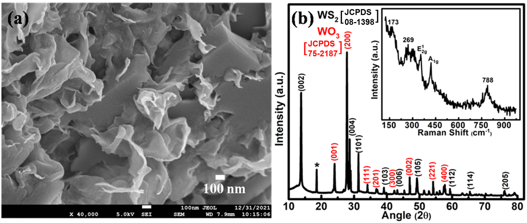 | ||
| Fig. 1 (a) FESEM micrograph; (b) XRD pattern of WS2/WO3 nanoflakes along with their Raman spectra (inset). | ||
As planned, the above-characterized nanoflakes of WS2/WO3 have been used as a dopant to make a multifunctional solid-state ECD by following the recipe mentioned in the experimental section. The ECD having structure “ITO glass/P3HT/(WO3/WS2 + EV)/ITO” glass was obtained by sandwiching the P3HT and EV (doped with WO3/WS2) in PEO gel electrodes, as shown in the schematic (Fig. 2(a)). The finally prepared device appears in its magenta color due to the inherent color of pristine P3HT with the EV layer being transparent. As the external power supply (+1.5 V, with respect to P3HT) is applied across the two different electrodes of the device, the device changes its initial magenta color to blue color as shown in the actual photographs of the device (inset, Fig. 2(a)). This is because of the reduction of the EV2+ ion to its EV˙+ radical cation and comes from its transparent state to a blue state.45 Subsequently, neutral P3HT gets oxidized by losing its electron to the electrode and changes its magenta color to its transparent color through a dynamic doping process. Thus, the simultaneous change in the color of both electrodes gives the overall blue color to the device, which can also be understood using the bias-dependent UV-Vis transmission spectra of the device as has been discussed later on. On reversing the bias polarity (−1.5 V), the device comes back to its magenta color (Fig. 2(b)) due to the bias reversal redox behavior of both the EV and P3HT electrodes.
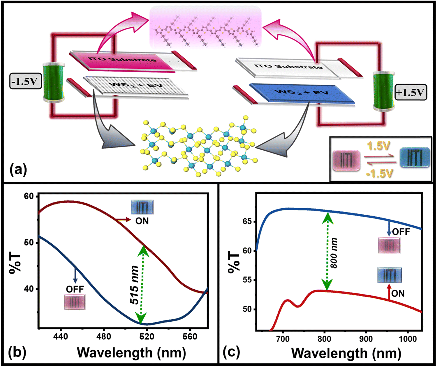 | ||
| Fig. 2 (a) Schematic representation of the layered device along with its actual photographs (inset) under different bias conditions, (b) in situ bias dependent transmission spectra of the device in the visible (∼515 nm) as well as NIR (∼800 nm) wavelength region in (c). Graphics Partly adopted with permission from ref. 26 Copyright American Chemical Society (2023). | ||
The color change of the device can also be understood by the bias-dependent transmission spectra of the device (Fig. 2(b) and (c)), which shows the change in optical transmittance of the device as a function of applied bias and can be correlated with the perceived color of the device. The maximum transmission occurs in the blue and red wavelength regions of the visible spectrum, which gives the initial (magenta, OFF) color to the device (blue curve, Fig. 2(b)) whereas the colored (blue or “ON”) state is characterized by the overall transmission band in the lower energy (blue wavelength) region (red curve, Fig. 2(b)) and giving the blue appearance to the device. There is an increased transmission of IR-radiation in the OFF state of the device whereas suppressed transmission in the IR-radiation value, as a function of applied bias. It can be appreciated from Fig. 2(c), which shows the multiwavelength transmission modulation of the device in the visible (∼515 nm) as well as NIR (∼800 nm) wavelength regions. The device has sufficiently good color contrast in the visible wavelength region with a maximum value of ∼52% at 515 nm. The device shows reversible color switching between the two colors represented through the CIE color coordinates (u′,v′) of (0.381, 0.362) in the OFF state and (0.198, 0.262) in the ON state, as shown in Fig. 3. It also maintains its good contrast value corresponding to a higher wavelength in the near infrared (NIR) region. Therefore, these two wavelength regions have been chosen to carry out investigations related to the electrochromic switching behavior of the device by measuring its switching kinetics.
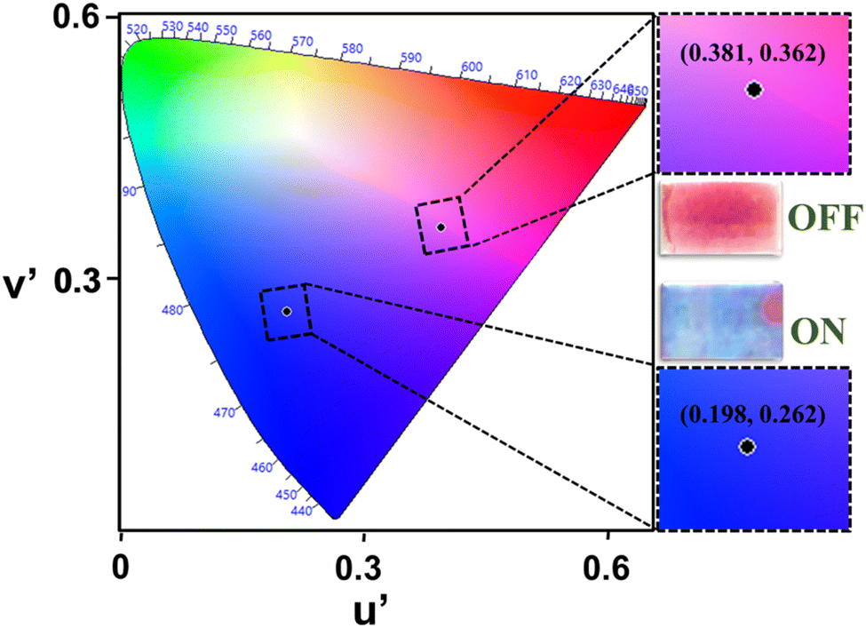 | ||
| Fig. 3 Color identification through the CIE chart of the fabricated device and the corresponding images. | ||
In addition to the color contrast of the device, switching stability/cyclability is another important parameter, when we examine the electrochromic performance of an electrochromic device (Fig. 4). The device shows excellent switching stability of at least 1000 seconds when the device is continuously toggled between ON/OFF states with an applied square pulse of ±1.5 V amplitude of 5 s time intervals each at 515 nm and 800 nm wavelength regions, respectively. The ECD exhibited less variation in absorbance even after the 200 repeated operation cycles in the visible (∼515 nm, Fig. 4(a)) wavelength region whereas the repeated switching cycles in the infrared (IR) (∼800 nm) region show some spikes in the absorbance values due to the external environmental disturbance while recording the repeating switching cycles of the device (Fig. 4(b)). The significantly lower variation in absorbance in the repetition of such switching steps up to 1000 s or 200 switching cycles shows a great stability/cyclability of the device in both wavelength regions.
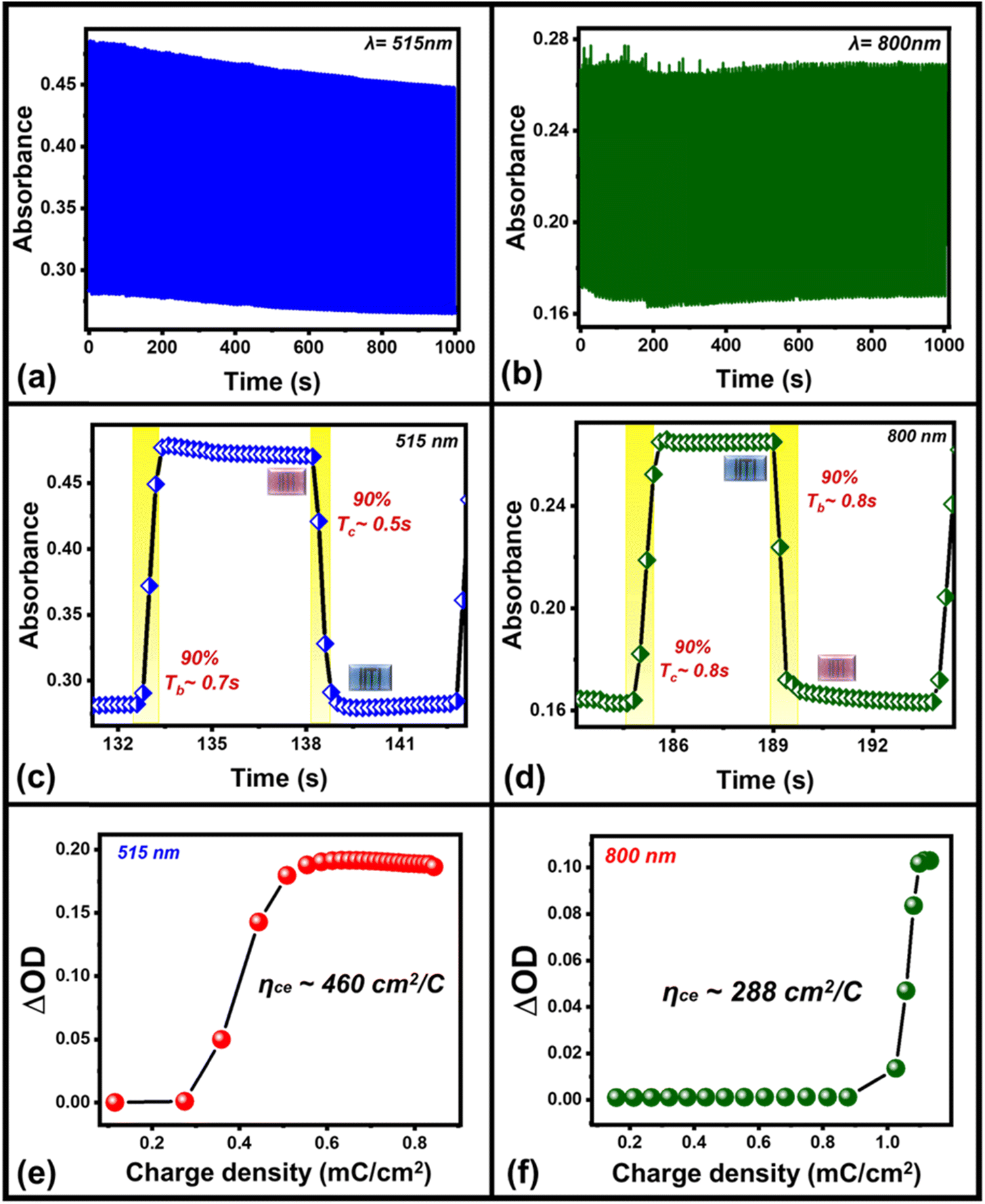 | ||
| Fig. 4 (a) In situ bias-dependent multiple switching cycles of the device between ON and OFF states in the voltage window (±1.5 V) in the visible and infrared (IR) wavelength region in (b) and (c) single switching cycle at 515 nm wavelength, (d) response time of the device in the same fixed voltage window at 800 nm wavelength, and the corresponding estimated coloration efficiencies of the device in (e) and (f). | ||
One of these absorbance switching cycles has been used to measure the switching time taken by the device to toggle between its ON and OFF states (Fig. 4(c) and (d)). The switching time is defined as the time taken by the device to show 90% change in the absorbance value. The as-prepared device takes 500 ms to switch from its OFF state (magenta) to ON state (blue), while 700 ms is required to switch back to the OFF state from the ON state in the visible (∼515 nm) wavelength region (Fig. 4(c)) whereas its switching time in the IR-wavelength (∼800 nm) region is 0.8 s (coloration, ON)/0.8 s (bleaching, OFF), respectively (Fig. 4(d)). A switching time of less than a second shown by the device represents a fast switching that has been achieved due to the presence of the mixture of WS2/WO3 as it can store charge carriers under external bias, which facilitates the necessary charges to take part in reversible redox reaction to P3HT in ECD that can be compared with the device in the absence of the mixture of WS2/WO3 (Fig. S2, ESI†). Additionally, the coloration efficiency (CE)46,47 is one of the most crucial parameters to measure the performance of an ECD in terms of the overall power efficiency, which is estimated by the formula given in eqn (1) below:
 | (1) |
| S. no | Device composition | Switching time (s) | Coloration efficiency (cm2 C−1) | Ref. |
|---|---|---|---|---|
| 1 | P3HT-NTTO | 0.8 | 1055 | Bansal et al.26 |
| 2 | PANI/P3HT | 0.5 | 534 | Pathak et al.48 |
| 3 | P3HT/PCBM | 0.5 | 320 | Chaudhary et al.49 |
| 4 | P3HT/IAI/PET | 0.3 | 252 | Kim et al.50 |
| 5 | P3HT/viologen | 1.5 | 200 | Chaudhary et al.38 |
| 6 | P3HT/WO3 + WS2 + EV | 0.5 | 460 | This work |
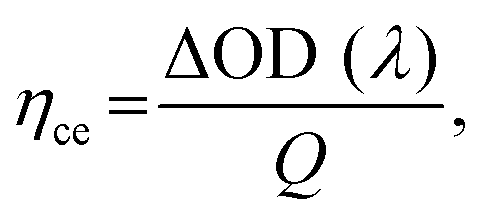
The (super-)capacitive property of the electrochromic device has also been optimized through cyclic voltammetry (CV), electrochemical impedance spectroscopy (EIS), and galvanostatic charge–discharge (GCD) curves. The CV curves of the fabricated solid-state ECD at different scan rates from 100 mV s−1 to 400 mV s−1 with the potential range of −1.5 V to 2 V have been recorded (Fig. 5(a)) which shows a pair of redox peaks indicating pseudocapacitive behavior of WS2/WO3 nanoflakes. Furthermore, the movement of ion diffusion in an electrochromic device has been investigated by EIS using a Nyquist plot (Fig. 5(b)) up to the frequency range of 100 kHz to 10 mHz. The Nyquist plot exhibits a semicircle and linear regiment representing high- and low-frequency regions, respectively. The semi-circle in the high-frequency region is associated with the contact resistance between the solution and electrolyte whereas the linear regiment at the low-frequency region associated with the redox mechanism occurs at the electrode–electrolyte interface, which indicates the capacitive behavior of the fabricated hybrid electrochromic device. To fit the EIS analysis data, an equivalent electrical circuit (inset, Fig. 5(b)) has been plotted, which shows the small charge transfer resistance, indicating fast charging and discharging response time of the device.
 | ||
| Fig. 5 (a) Cyclic voltammetry of the device for different scan rates, (b) Nyquist plot (inset: equivalent electric circuit), (c) charging/discharging curves with increasing current densities and (d) varying specific capacitance value along with the energy density variation of the device in the inset. | ||
Furthermore, the electrochemical performance of the device has been investigated through the galvanostatic charge/discharge curve with different current densities (1 A g−1 to 2 A g−1) using a potential window from 1.6 V to −1.6 V. The deviation from the ideal triangular shape of the GCD curves indicates the contribution from the pseudocapacitive charge storage behavior of the device. The small infrared (IR) drop present in the GCD curves of the device also shows the small charge transfer resistance offered by the electrolyte ions as also expected from the EIS plot. It is also clearly seen that the discharging time decreases with the increase in the current density due to the faster diffusion of electrolyte ions on the active material of the device. A bit longer discharging time, than charging time, indicates the high Coulombic efficiency of the device, which makes it suitable for practical applications. This can also be seen in the recorded time dependent absorbance spectrum curve (Fig. S3, ESI†) of the device during charging and discharging, which also shows the decreasing absorbance value during the discharging process, which is one of the crucial factors for electrochromic supercapacitors. Furthermore, the specific capacitance51,52 of the device has been calculated from a GCD plot using the equation (eqn (2)) mentioned below:
 | (2) |
 | (3) |
Based on the above discussion, it is very clearly evident that a solid-state electrochromic device vis-e-vis ITO/(EV + WS2/WO3)/P3HT/ITO shows not only an improvement in electrochromic performance but also displays moderately high super capacitive performance. The two properties, namely improved electrochromic performance and charge storage capabilities, are complementary to each other and support mutual operation. Incorporation of WS2/WO3 plays a key role by storing charge to facilitate the necessary redox process in a better way as well as thus assisting in necessary charge transport during color switching of the device. This yields a better way to make an improved multifunctional solid state electrochromic device made using complementing redox active layers. In other words, the WS2/WO3 doping enables one to achieve (i) improved dual band electrochromic modulation in the visible and NIR range and (ii) multifunctional operation by adding charge storage making it an overall multifunctional electrochromic solid state device.
4. Conclusion
A multifunctioning all-organic solid-state electrochromic device with supercapacitance charge storage capabilities can be fabricated using WS2/WO3 nanoflakes. The well characterized WS2/WO3 nanoflakes when doped with the organic electrochromic materials, P3HT and EV, display power efficient multifunctional applications with a color switching between magenta and blue colors with a small bias of ±1.5 V. The device shows a great contrast ratio of 52%, fast switching time of less than one second and excellent coloration efficiencies of 460 cm2 C−1 and 288 cm2 C−1 at wavelengths ∼515 nm (visible), and ∼800 nm (NIR), respectively. Additionally, the device exhibited a maximum capacitance of ∼50 F g−1 and an energy density of ∼60 W h kg−1 at a current density of 1 A g−1. Furthermore, the GCD curves of the device show excellent response time and high coulombic efficiency with the increase in current density, making it suitable for practical applications. The improved electrochromic super capacitive device originates from the mutually supporting redox behavior of the P3HT, EV, and charge-facilitating nature of WS2/WO3. The WS2/WO3 doping in an all-organic material combines two applications, namely improved dual band electrochromic modulation in the visible and NIR range and charge storage, making it an overall multifunctional electrochromic solid-state device where the latter itself shows switching in the dual color band.Data availability statement
The data that supports the findings of this study are available within the article and ESI.†Conflicts of interest
There are no conflicts to declare.Acknowledgements
The authors acknowledge financial support from Science and Engineering Research Board, Government of India (grant no. CRG/2022/002787; CRG/2019/000371) and Indo German Science and Technology Centre (IGSTC grant number: IGSTC/SING-2022/40/2021-22/336). Authors T. G. and B. S. acknowledge IIT Indore for the fellowship. The DST, Govt. of India, is acknowledged for providing a fellowship to C. R. (DST/INSPIRE/03/2019/002160/IF190314). Authors S. K. and L. B. acknowledge UGC (Ref. 1304-JUNE-2018-513215) and CSIR (09/1022(12309)/2021-EMR-I), Govt. of India for providing fellowships. Author D. K. R. acknowledges UGC (Ref. 211610006497) Govt. of Indi, for providing fellowships. Raman Spectroscopy (IIT Indore) and XRD facilities (GJU) received from Department of Science and Technology (DST), Government of India, under FIST scheme (grant SR/FST/PSI-225/2016) are highly acknowledged. Authors I. Sameera & R. Bhatia are thankful to Department of Science and Technology (DST), New Delhi (India) for the financial support in the form of Inspire Faculty Awards (DST/INSPIRE04/2017/002776 & DST/INSPIRE/04/2015/000902). Technical assistance from Dr N. Upadhyay and Mr Prashant Gupta is also acknowledged.References
- R. Kumar, R. G. Pillai, N. Pekas, Y. Wu and R. L. McCreery, J. Am. Chem. Soc., 2012, 134, 14869–14876 CrossRef CAS PubMed.
- Y. Alesanco, A. Viñuales, J. Palenzuela, I. Odriozola, G. Cabañero, J. Rodriguez and R. Tena-Zaera, ACS Appl. Mater. Interfaces, 2016, 8, 14795–14801 CrossRef CAS PubMed.
- T. Ghosh, S. Kandpal, C. Rani, A. Chaudhary and R. Kumar, Adv. Opt. Mater., 2023, 11, 2203126 CrossRef CAS.
- A.-L. Alexe-Ionescu, A. Th Ionescu, N. Scaramuzza, G. Strangi, C. Versace, G. Barbero and R. Bartolino, Phys. Rev. E: Stat., Nonlinear, Soft Matter Phys., 2001, 64, 011708 CrossRef CAS PubMed.
- F. G. K. Baucke, K. Bange and T. Gambke, Displays, 1988, 9, 179–187 CrossRef CAS.
- X. Chen, H. Lin, J. Deng, Y. Zhang, X. Sun, P. Chen, X. Fang, Z. Zhang, G. Guan and H. Peng, Adv. Mater., 2014, 26, 8126–8132 CrossRef CAS PubMed.
- S. Kandpal, T. Ghosh, C. Rani, A. Chaudhary, J. Park, P. S. Lee and R. Kumar, ACS Energy Lett., 2023, 8, 1870–1886 CrossRef CAS.
- Y. Guo, W. Li, H. Yu, D. F. Perepichka and H. Meng, Adv. Energy Mater., 2017, 7, 1601623 CrossRef.
- T. S. Hernandez, C. J. Barile, M. T. Strand, T. E. Dayrit, D. J. Slotcavage and M. D. McGehee, ACS Energy Lett., 2018, 3, 104–111 CrossRef CAS.
- X. Guo, J. Chen, A. L.-S. Eh, W. C. Poh, F. Jiang, F. Jiang, J. Chen and P. S. Lee, ACS Appl. Mater. Interfaces, 2022, 14, 20237–20246 CrossRef CAS PubMed.
- A. Chaudhary, D. K. Pathak, M. Tanwar, J. Koch, H. Pfnür and R. Kumar, J. Mater. Chem. C, 2020, 8, 1773–1780 RSC.
- H. J. Lee, C. Lee, J. Song, Y. J. Yun, Y. Jun and C. S. Ah, J. Mater. Chem. C, 2020, 8, 8747–8754 RSC.
- A. S. Shaplov, D. O. Ponkratov, P.-H. Aubert, E. I. Lozinskaya, C. Plesse, F. Vidal and Y. S. Vygodskii, Chem. Commun., 2014, 50, 3191–3193 RSC.
- S. Y. Kim, T. Y. Yun, K. S. Yu and H. C. Moon, ACS Appl. Mater. Interfaces, 2020, 12, 51978–51986 CrossRef CAS PubMed.
- X. Xia, Y. Zhang, D. Chao, C. Guan, Y. Zhang, L. Li, X. Ge, I. Mínguez Bacho, J. Tu and H. Jin Fan, Nanoscale, 2014, 6, 5008–5048 RSC.
- S. Kandpal, T. Ghosh, C. Rani, M. Tanwar, M. Sharma, S. Rani, D. K. Pathak, R. Bhatia, I. Sameera, J. Jayabalan and R. Kumar, ACS Mater. Au, 2022, 2, 293–300 CrossRef CAS PubMed.
- S. Li, Y. Wang, J.-G. Wu, L. Guo, M. Ye, Y.-H. Shao, R. Wang, C. Zhao and A. Wei, RSC Adv., 2016, 6, 72037–72043 RSC.
- A. Chaudhary, D. K. Pathak, T. Ghosh, S. Kandpal, M. Tanwar, C. Rani and R. Kumar, ACS Appl. Electron. Mater., 2020, 2, 1768–1773 CrossRef CAS.
- S. Kandpal, T. Ghosh, M. Sharma, D. K. Pathak, M. Tanwar, C. Rani, R. Bhatia, I. Sameera, A. Chaudhary and R. Kumar, Appl. Phys. Lett., 2021, 118, 153301 CrossRef CAS.
- T. Ghosh, S. Kandpal, C. Rani, L. Bansal, M. Tanwar and R. Kumar, Adv. Electron. Mater., 2023, 9, 2201042 CrossRef CAS.
- C. Liu, Y. Bai, W. Li, F. Yang, G. Zhang and H. Pang, Angew. Chem., Int. Ed., 2022, 61, e202116282 CrossRef CAS PubMed.
- J.-L. Yang, J.-M. Cao, X.-X. Zhao, K.-Y. Zhang, S.-H. Zheng, Z.-Y. Gu and X.-L. Wu, EnergyChem, 2022, 4, 100092 CrossRef CAS.
- P. Geng, L. Wang, M. Du, Y. Bai, W. Li, Y. Liu, S. Chen, P. Braunstein, Q. Xu and H. Pang, Adv. Mater., 2022, 34, 2107836 CrossRef CAS PubMed.
- G. Cai, J. Wang and P. S. Lee, Acc. Chem. Res., 2016, 49, 1469–1476 CrossRef CAS PubMed.
- W. Guo, Z. Cong, Z. H. Guo, P. Zhang, Y. Chen, W. Hu, Z. L. Wang and X. Pu, Adv. Funct. Mater., 2021, 31, 2104348 CrossRef CAS.
- L. Bansal, T. Ghosh, S. Kandpal, C. Rani, M. Tanwar and R. Kumar, ACS Appl. Eng. Mater., 2023, 1, 577–583 CrossRef CAS.
- L. Groenendaal, F. Jonas, D. Freitag, H. Pielartzik and J. R. Reynolds, Adv. Mater., 2000, 12, 481–494 CrossRef CAS.
- B.-R. Huang, T.-C. Lin and Y.-M. Liu, Sol. Energy Mater. Sol. Cells, 2015, 133, 32–38 CrossRef CAS.
- K. Ahmad, M. A. Shinde, G. Song and H. Kim, Ceram. Int., 2021, 47, 34297–34306 CrossRef CAS.
- K.-W. Kim, T. Y. Yun, S.-H. You, X. Tang, J. Lee, Y. Seo, Y.-T. Kim, S. H. Kim, H. C. Moon and J. K. Kim, NPG Asia Mater., 2020, 12, 1–10 CrossRef.
- C. C. Mayorga-Martinez, A. Ambrosi, A. Y. S. Eng, Z. Sofer and M. Pumera, Electrochem. Commun., 2015, 56, 24–28 CrossRef CAS.
- A. Azam, J. Kim, J. Park, T. G. Novak, A. P. Tiwari, S. H. Song, B. Kim and S. Jeon, Nano Lett., 2018, 18, 5646–5651 CrossRef CAS PubMed.
- K. S. Kumar, N. Choudhary, D. Pandey, L. Hurtado, H.-S. Chung, L. Tetard, Y. Jung and J. Thomas, Nanotechnology, 2020, 31, 435405 CrossRef CAS PubMed.
- V. V. Mohan, M. Manuraj, P. M. Anjana and R. B. Rakhi, Energy Technol., 2022, 10, 2100976 CrossRef CAS.
- Y. Wang, D. Kong, W. Shi, B. Liu, G. J. Sim, Q. Ge and H. Y. Yang, Adv. Energy Mater., 2016, 6, 1601057 CrossRef.
- Q. Liu, X. Li, Z. Xiao, Y. Zhou, H. Chen, A. Khalil, T. Xiang, J. Xu, W. Chu, X. Wu, J. Yang, C. Wang, Y. Xiong, C. Jin, P. M. Ajayan and L. Song, Adv. Mater., 2015, 27, 4837–4844 CrossRef CAS PubMed.
- L. Wang, K. Wang, R. Huang, Z. Qin, Y. Su and S. Tong, Chemosphere, 2020, 252, 126578 CrossRef CAS PubMed.
- A. Chaudhary, D. K. Pathak, S. Mishra, P. Yogi, P. R. Sagdeo and R. Kumar, Sol. Energy Mater. Sol. Cells, 2018, 188, 249–254 CrossRef CAS.
- S. V. P. Vattikuti, C. Byon and V. Chitturi, Superlattices Microstruct., 2016, 94, 39–50 CrossRef CAS.
- I. Sharma, M. M. Ghangrekar, R. C. Biswal and K. Biswas, J. Electrochem. Soc., 2015, 163, F183 CrossRef.
- Y. Li, Z. Tang, J. Zhang and Z. Zhang, Appl. Catal., B, 2017, 207, 207–217 CrossRef CAS.
- V. N. Tuan, H. H. Do, T. Mahider, V. L. Quyet, N. T. Phan, S. H. Hong, J. H. Cho, V. D. Dung, S. H. Ahn and K. S. Young, Nano Convergence, 2021, 8, 28 CrossRef PubMed.
- H. Zeng, G.-B. Liu, J. Dai, Y. Yan, B. Zhu, R. He, L. Xie, S. Xu, X. Chen, W. Yao and X. Cui, Sci. Rep., 2013, 3, 1608 CrossRef PubMed.
- L. Yuan and L. Huang, Nanoscale, 2015, 7, 7402–7408 RSC.
- S. Mishra, H. Pandey, P. Yogi, S. K. Saxena, S. Roy, P. R. Sagdeo and R. Kumar, Opt. Mater., 2017, 66, 65–71 CrossRef CAS.
- S.-H. Lee, H. M. Cheong, C. E. Tracy, A. Mascarenhas, A. W. Czanderna and S. K. Deb, Appl. Phys. Lett., 1999, 75, 1541–1543 CrossRef CAS.
- S. Kandpal, T. Ghosh, C. Rani, S. Rani, D. K. Pathak, M. Tanwar, R. Bhatia, I. Sameera and R. Kumar, Sol. Energy Mater. Sol. Cells, 2022, 236, 111502 CrossRef CAS.
- D. K. Pathak, T. Ghosh, S. Kandpal, C. Rani and R. Kumar, Opt. Mater., 2023, 137, 113519 CrossRef CAS.
- A. Chaudhary, D. K. Pathak, M. Tanwar, P. Yogi, P. R. Sagdeo and R. Kumar, ACS Appl. Electron. Mater., 2019, 1, 58–63 CrossRef CAS.
- T.-H. Kim, S.-H. Park, D.-H. Kim, Y.-C. Nah and H.-K. Kim, Sol. Energy Mater. Sol. Cells, 2017, 160, 203–210 CrossRef CAS.
- H. Teng, J. Song, G. Xu, F. Gao and X. Luo, Electrochim. Acta, 2020, 355, 136772 CrossRef CAS.
- M. K. Singh, A. K. Gupta, S. Krishnan, N. Guha, S. Marimuthu and D. K. Rai, J. Energy Storage, 2021, 43, 103301 CrossRef.
- X. Li, Y. Ma, P. Shen, C. Zhang, M. Cao, S. Xiao, J. Yan, S. Luo and Y. Gao, Adv. Mater. Technol., 2020, 5, 2000272 CrossRef CAS.
- K. L. Van Aken, M. Beidaghi and Y. Gogotsi, Angew. Chem., Int. Ed., 2015, 127, 4888–4891 CrossRef.
Footnotes |
| † Electronic supplementary information (ESI) available: In situ absorbance performance, EDS profile, and absorbance curve during charging/discharging. See DOI: https://doi.org/10.1039/d3tc01880f |
| ‡ Current address: Department of Chemistry, University of Michigan, Ann Arbor, Michigan 48109, United States of America. |
| This journal is © The Royal Society of Chemistry 2023 |