
One-dimensional lead-free perovskite single crystals with high X-ray response grown by liquid phase diffusion†
Chang-Feng
Wang‡
 ,
Cui-Ling
Fang‡
,
Yan
Feng
,
Shi-Yu
Liu
,
Yi
Zhang
,
Heng-Yun
Ye
,
Le-Ping
Miao
and
Lang
Liu
*
,
Cui-Ling
Fang‡
,
Yan
Feng
,
Shi-Yu
Liu
,
Yi
Zhang
,
Heng-Yun
Ye
,
Le-Ping
Miao
and
Lang
Liu
*
Chaotic Matter Science Research Center, Department of Materials, Metallurgy and Chemistry, Jiangxi University of Science and Technology, Ganzhou 341000, China. E-mail: amn716@163.com
First published on 30th November 2022
Abstract
Organic–inorganic hybrid bismuth halides, as essential members of the lead-free family, have attracted much attention due to their unique properties. However, the growth of bismuth-based single crystals with potentially low defect density has encountered many challenges, such as intractable rapid crystallization, the use of toxic organic solvents, and halide oxidation caused by prolonged heating. Herein, we developed a liquid phase diffusion method to prepare large-sized one-dimensional hybrid bismuth single crystals. Adopting this method, centimeter-sized (1,5-pentanediamine)BiI5 single crystals were harvested, which possess a hole trap density as low as 1.31 × 109 cm−3 and a carrier mobility reaching 28.2 cm2 V−1 s−1. The X-ray detectors based on (1,5-pentanediamine)BiI5 single crystals exhibit a sensitivity value of 8120 μC Gyair−1 cm−2 at −80 V. This work provided a new strategy for the growth of bismuth-based perovskite single crystals and inspired the growth of other hybrid perovskite materials.
Introduction
X-ray detectors are widely used in computed tomography, nondestructive product inspection, scientific research, etc.1–3 At present, two detector technologies prevail: the indirect scintillator and the direct photoconductor.4 Between them, the semiconductor-based direct conversion form has attracted more attention as it outperformed the scintillators in the aspect of device configuration and detection sensitivity. Currently, the most advanced and popular direct X-ray imaging system is based on amorphous selenium (α-Se). However, its charge transport properties and X-ray stopping capacity are still far from satisfactory. Accordingly, candidates with high X-ray absorption capacity (e.g. PbI2, CdZnTe, and HgI2) have been extensively developed.5 Although the emergence of these candidates partially fulfilled the expectations, it also caused other challenges inherently. For instance, the growth of high-quality CdZnTe needs a processing temperature of 600 °C, far beyond the heat resistance limit of thin-film transistors.6 Recently, organic–inorganic hybrid lead halide perovskites have been recognized as a dark horse for the development of direct X-ray imaging due to their solution-processability, structural diversity, and excellent photophysical properties.7–12 Detectors based on the perovskites demonstrated astounding performance, e.g. ultra-high sensitivity,13 an extremely low detection limit,14 and rapid light response.15,16 Despite the abovementioned substantial advances, the use of lead has also raised environmental concerns.17–20Theoretically, the X-ray absorption coefficient of an element is proportional to its atomic number.21 Bismuth not only possesses a higher atomic number but also its trivalent ions share the same electronic configuration with Pb2+.20,22–25 Therefore, bismuth-based hybrid halide perovskites, as a class of lead-free members, provides potential new players for high-performance detection materials as exemplified by (3-(aminomethyl)pyridine)BiI5, (benzamidinium)BiI4, MA3Bi2I9, (CH3NH3CH2CH2NH3CH3)BiI5 and (N-methyl-1,3-diaminopropanium)BiI5.17,26–30 In addition to enriching the bismuth-based perovskite family, researchers have also made a lot of attempts in crystal growth methods. For example, using the antisolvent vapor-assisted method, centimeter-sized 1D (pentamethylenediamine)BiBr5 single crystals (SCs) were obtained.31 With the help of the top-seeded solution growth method, Luo's group prepared large-sized 1D (N-methyl-1,3-diaminopropanium)BiI5.29 Employing a temperature cooling method, (3-(aminomethyl)pyridine)BiI5 as well as (CH3NH3CH2CH2NH3CH3)BiI5 SCs were also harvested.17,28 Additionally, the inverse temperature crystallization method was also adopted to prepare 0D MA3Bi2I9 SCs from γ-butyrolactone solution.27 Despite recent blooming advances, the aforementioned methods still suffer from some drawbacks. The top-seeded solution growth method, inverse temperature crystallization method, and temperature cooling method, usually require long periods of heating, which inevitably triggers I− oxidation, greatly impairing crystal quality32–35 while the antisolvent vapor method often needs toxic organic solvents such as toluene and dichloromethane. Moreover, the crystallization properties and kinetics of Bi-based perovskites are also significantly different from those of the lead ones, e.g. Bi-based perovskite precursors convert into target phase directly without mediating through crystalline solvated phases.36–38 In these aspects, the crystallization of Bi-based perovskites should be comprehensively considered in the context of growth methods and their own features.
In this work, we first studied the solubility of Bi-based perovskite and its corresponding precursors and found that there is a huge discrepancy between them. Specifically, the solubility of the BiI3 is more than 100 times that of the target product. Such a huge gap leads to the precipitation of a large number of microcrystals. Based on this understanding, we propose a liquid phase diffusion (LPD) growth strategy to control the precipitation amount of crystal nucleus, which allows harvesting of centimeter-sized single crystals (SCs). X-ray detectors based on the prepared (1,5-PDA)BiI5 (1,5-PDA is 1,5-pentanediamine) SCs deliver a sensitivity value of 8120 μC Gyair−1 cm−2 under −80 V. Our finding provides new insight into SC growth, which expands the crystal growth spectrum of mixed perovskite materials. This strategy can also be easily extended to other perovskite-based materials to improve their optoelectronic performance.
Results and discussion
Crystal structure of (1,5-PDA)BiI5
We first use the popular temperature cooling method to grow (1,5-PDA)BiI5 SCs (the detailed method can be seen in the ESI†). At room temperature, (1,5-PDA)BiI5 crystallizes in the orthorhombic space group of P212121 (point group of 222) with cell parameters: a = 8.5824(4) Å, b = 14.7005(7) Å, c = 14.1760(7) Å, and V = 1788.52(15) Å3, of which asymmetric unit consists of one BiI5− anion and one protonated 1,5-PDA cation (Table S1, ESI†). Each Bi3+ metal cation is coordinated with six I− anions to form a BiI6 octahedron, in which four I− anions are terminal and two act as a bridge to connect two neighboring BiI6 octahedrons, showing that 1D corner-shared (BiI5)n2n− zigzag chains extend infinitely along a-axis direction, as shown in Fig. 1. The Bi–I bond distances range from 2.8928(11) to 3.3144(10) Å; I–Bi–I bond angles range from 83.990(13) to 97.90(3)°, Table S2 and S3 (ESI†). Δd (distortion index) and σ2 (bond angle variance) were employed to evaluate the distortion level of the BiI6 octahedrons, respectively (the detailed calculation process can be seen in the ESI†). Δd and σ2 were separately calculated to be 0.03909 and 18.55°,2 indicating significant distortion. The 1,5-PDA organic cations occupied the cavities that can be seen to be composed of the four (BiI5)n2n− zigzag chains (Fig. S1, ESI†). As shown in Fig. S2a (ESI†), the Hirshfeld surface mapped with dnorm (normalized contact distance) disclose that the main interaction between organic cations and inorganic formwork is N–H⋯I Hydrogen bonds range from 2.766 to 2.875 Å. Fingerprint plots suggest N–H⋯I Hydrogen is 75.3% of the total Hirshfeld surface as shown in Fig. S2b (ESI†).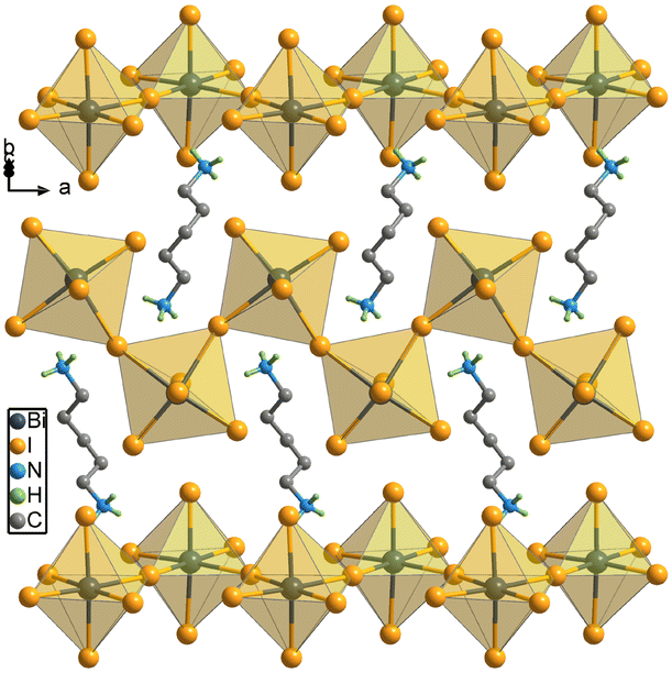 | ||
| Fig. 1 The packing structure of (1,5-PDA)BiI5. | ||
Growth and optimization of (1,5-PDA)BiI5 SCs
During the aforementioned temperature cooling process, we found that the colour of the solution turned into black from pale yellow, suggesting severe oxidation of iodide ions after a long period of continuous heating.39 Moreover, we found it difficult to control the number of precipitated nuclei as evidenced by a large amount of microcrystals were obtained at the bottom of the flask. Further experiments show that there is a huge difference in solubility between the precursors and target products. By contrast to the good solubility of 1,5-PDAI2 (2.14 mmol ml−1) and BiI5 (3.88 mmol ml−1) in hydroiodic acid, the solubility of the (1,5-PDA)BiI5 is as low as 0.0348 mmol ml−1, even if the hydroiodic acid is heated to near boiling point (127 °C), the solubility of the (1,5-PDA)BiI5 can only reach 0.0875 mmol ml−1 (Fig. 2a). Due to such a low solubility, a large number of (1,5-PDA)BiI5 crystallites formed rapidly once the precursors mixed together, hindering further growth of single-crystals. The process of crystallization can be divided into two steps: nucleation and growth.3 Clearly, in our case, the key factor for growing large-sized and high-quality SCs is how to effectively control the number of nuclei. Based on the above analysis, we developed the LPD method to grow (1,5-PDA)BiI5 SCs. Briefly, it is carried out in an H-shaped test tube composed of three parts (A, B, and C), as shown in Fig. 2b. First, hydroiodic acid containing BiI5 and 1,5-PDAI2 were added into test tubes A and C, respectively. Then hydroiodic acid acting as a buffer to prevent the formation of a large number of (1,5-PDA)BiI5 crystallites was carefully injected into test tube B. As time goes on, precursor 1,5-PDAI2 in test tube A and BiI5 in test tube C would continually diffuse into the middle of test tube B. When the concentration of (1,5-PDA)BiI5 in the middle of test tube B reaches supersaturation, crystal nuclei would be formed. The formation of crystal nuclei would decrease the concentration of BiI5 and 1,5-PDAI2 around crystal nuclei, which brings about the concentration gradient. Therefore, 1,5-PDAI2 and BiI5 would resume diffusion toward crystal nuclei and crystal nuclei would continually grow. Notably, the diffusion of precursors and crystal growth are synchronous. After a month, black crystals were obtained in the middle of the test tube B.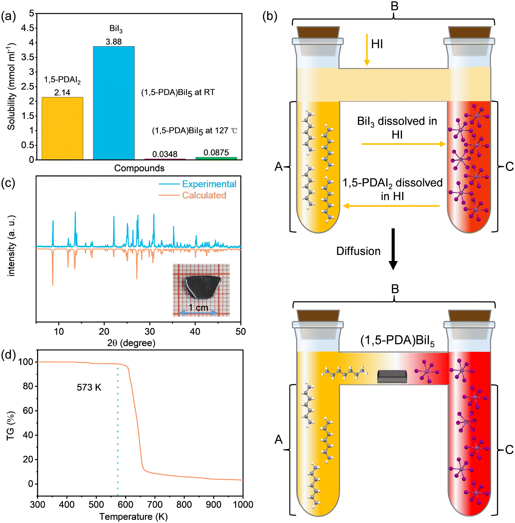 | ||
| Fig. 2 (a) Solubility of precursors and target product. (b) The schematic diagram for (1,5-PDA)BiI5 large-sized single-crystal growth using the LPD method. (c) Comparison between experimental PXRD pattern and calculated counterpart. Inset: Optical image of the SC of (1,5-PDA)BiI5. (d) TG measurement for (1,5-PDA)BiI5. | ||
The digital photograph of the as-prepared (1,5-PDA)BiI5 SC is presented in the inset of Fig. 2c. The powder X-ray diffraction measurements verified the phase purity of (1,5-PDA)BiI5 (Fig. 2c). Thermogravimetric (TG) measurement was adopted to evaluate the thermal stability. As shown in Fig. 2d, there is no obvious mass loss until 573 K, suggesting the decomposition of (1,5-PDA)BiI5 greater than this temperature.
The UV-vis absorption spectrum of (1,5-PDA)BiI5 was recorded for evaluation of the potential of (1,5-PDA)BiI5 in photoelectronic applications. As shown in Fig. 3a, there is an absorption edge at about 650 nm. By fitting variant Tauc equation (the detailed process can be seen in ESI†), the optical band gap of (1,5-PDA)BiI5 was determined to be 1.95 eV, which is close to MA3Bi2I9 of 1.99 eV,27 and greater than (3-(aminomethyl)pyridine)BiI5 of 1.74 eV,17 (benzamidinium)BiI4 of 1.77 eV,26 (N-methyl-1,3-diaminopropanium)BiI5 of 1.83 eV,29 and (CH3NH3CH2CH2NH3CH3)BiI5 of 1.86 eV.28 The theoretical calculations were further adopted to disclose the band gap characteristic of (1,5-PDA)BiI5. As shown in Fig. 3b, the bottom of the conduction band (CBM) and the top of the valence band (VBM) are both located at the G point, indicating a direct band gap similar to (CH3NH3CH2CH2NH3CH3)BiI5.28 The difference value between the CBM and the VBM, the calculated band gap, is approximately 2 eV, on par with that of the experimental result. The partial densities of states (PDOS) calculations were carried out to investigate the origin of the band gap of (1,5-PDA)BiI5. As shown in Fig. S3 (ESI†), the VBM mainly consists of I 5p orbitals with a small number of Bi 6s and 6p orbitals, while CBM originates from Bi 6p and I 5p orbitals.
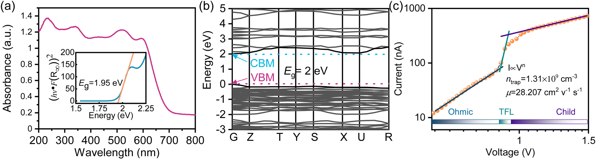 | ||
| Fig. 3 (a) UV-vis absorption spectra of (1,5-PDA)BiI5. Inset shows the Tauc plot of (1,5-PDA)BiI5. (b) Band structure of (1,5-PDA)BiI5. (c) Current–voltage curve of the (1,5-PDA)BiI5 SC device. | ||
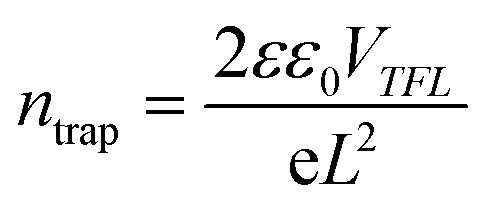
We further studied the trap density (ntrap) and carrier mobility (μ) of the prepared crystal based on the space charge-limited current (SCLC) method. As shown in Fig. 3c, the ohmic region, trap-filling region and the trap-free SCLC region can be identified clearly from the current–voltage curve. The hole trap density can be obtained from the following equation:
Device performance of (1,5-PDA)BiI5 SC X-ray detectors
Inspired by the prepared high-quality crystals, we then try to evaluate their performance as X-ray detectors. We first calculated the X-ray absorption coefficients of (1,5-PDA)BiI5 and several common traditional semiconductors by the photon cross-section database.1 As shown in Fig. 4a, the absorption coefficient of (1,5-PDA)BiI5 is much higher than that of the semiconductor Si and is close to that of the α-Se and CdTe within the photon energy range of 5 keV to 100 MeV. This is consistent with a fact that Bi possesses a higher atomic number and indicates its X-ray absorption capacity is similar to or even better than those of traditional semiconductors. Fig. 4b shows the relationship between the thickness and the attenuation efficiency of (1,5-PDA)BiI5 and several traditional detector materials at 40 keV X-ray photons. The attenuation efficiency of (1,5-PDA)BiI5 and several traditional semiconductor materials increases with the increase of thickness under irradiation. At the same thickness, the attenuation efficiency of (1,5-PDA)BiI5 is obviously higher than that of the Si and α-Se. Taking 0.5 mm as an example, (1,5-PDA)BiI5 attenuates 95% of the incident photons, while that of the Si and α-Se is only about 8% and 82%, respectively.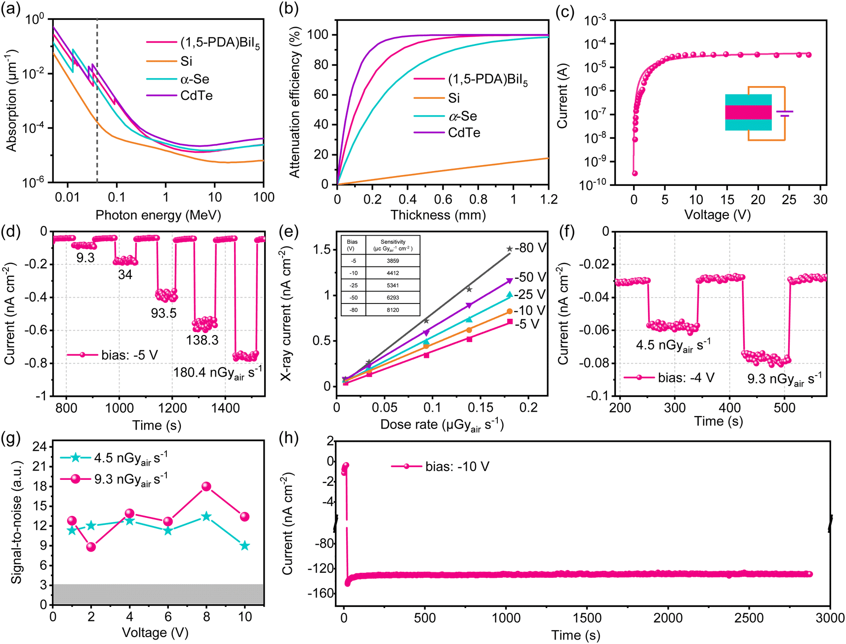 | ||
| Fig. 4 Performance of the (1,5-PDA)BiI5 SC X-ray detector. (a) Absorption coefficients of (1,5-PDA)BiI5, Si, α-Se, and CdTe as a function of photon energy. (b) Attenuation efficiency of (1,5-PDA)BiI5, Si, α-Se, and CdTe for 40 keV X-ray photons versus thickness. (c) Bias-dependent photoconductivity of the (1,5-PDA)BiI5 device. Inset: Schematic illustration of the device used for photoconductivity measurement. (d) Relationship between time and current density of (1,5-PDA)BiI5, (1,5-PDA)BiI5 device under −5 V bias voltage. (e) X-Ray response current at various dose rates (the sensitivity can be derived from the slope of the fitting line). (f) Representative photo-response curve under low dose rate radiation with a (1,5-PDA)BiI5 bias of −4 V. (g) Signal-to-noise ratio of the detector under low dose rate radiation with different bias voltage. (h) Device stability upon continuous radiation with a dose rate of 113.1 μGyair s−1 under −10 V. | ||
After undergoing a range of interactions between X-ray and detection materials, a massive amount of carriers were generated, whose lifetime and mobility product (μτ) determined the mean distance drifted under a unit electric field before recombination. This value was obtained by fitting the photoconductivity curve (Fig. 4c) based on the modified Hecht equation.2 The μτ product of the (1,5-PDA)BiI5 SC is 7.49 × 10⁻³ cm2 V−1, which is comparable to that of the CdZnTe (9.13 × 10⁻³ cm2 V−1)3 and is just slightly lower than that of the MAPbBr3 (1.43 × 10⁻² cm2 V−1).40 In order to study the detection performance of the device, we designed a parallel planar electrode, which consists of a 120 nm-thick Au. The detector sensitivity is an important parameter of advanced imaging, which is defined as the charge collected per unit area of radiation exposure (μC Gyair−1 cm−2). Fig. 4d shows the representative light response feature of the as-prepared detector under different dose rates (for other photoelectric response curves please see Fig. S4, ESI†). It displays a –42 pA cm−2 dark current without obvious drift during test that lasted more than ten minutes. Moreover, the on–off switching feature can also be clearly identified under low radiation dose rates, indicating excellent light response properties. The corresponding sensitivity (S) value can be obtained according to the following formula:
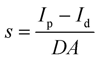
Encouraged by the aforementioned outstanding weak light response feature, we further studied the detection limit of the detector. IUPAC defines the detection limit as the equivalent dose rate that generates a signal greater than three times the noise level under a given electric field. The calculation formula for the signal-to-noise ratio is
Conclusions
In summary, the LPD method is demonstrated to control the precipitation amount of crystal nucleus which enables us to harvest centimeter-sized SCs in perovskite systems with huge solubility discrepancy. As a result, the harvested (1,5-PDA)BiI5 SCs show a low trap-state density of 1.31 × 109 cm−3 and a high carrier mobility of 28.207 cm2 V−1 s-1. X-ray detectors based on the prepared SCs not only delivered an impressive sensitivity value (8120 μC Gyair−1 cm−2), but also exhibited an ultra-low detection limit (4.5 nGyair s−1). We believe that this simple and feasible crystal growth method could be applied to the preparation of other materials.Author contributions
C.-F. Wang designed the single crystal growth method, prepared materials, determined the single crystal structure, carried out DFT calculations and wrote the original draft; C.-L. Fang prepared the devices, performed device performance measurements and wrote the original draft; Y. Feng prepared synthetic materials; S.-Y. Liu performed device performance measurements; Y. Zhang, H.-Y Ye and L.-P. Miao provided suggestions for the research. L. Liu wrote and revised draft. All authors have given approval to the final version of the manuscript.Conflicts of interest
There are no conflicts to declare.Acknowledgements
The authors acknowledge the support from the National Natural Science Foundation of China (22109057 and 21875093), the Natural Science Foundation of Jiangxi Province (20212BAB214021, 20204BCJ22015, and 20202ACBL203001), and the Science and Technology Project of Jiangxi Provincial Department of Education (GJJ200836 and GJJ210847).Notes and references
- M. Ahmadi, T. Wu and B. Hu, Adv. Mater., 2017, 29, 1605242 CrossRef PubMed.
- Y. Zhang, Y. Liu, Z. Xu, H. Ye, Z. Yang, J. You, M. Liu, Y. He, M. G. Kanatzidis and S. F. Liu, Nat. Commun., 2020, 11, 2304 CrossRef CAS PubMed.
- Y. Liu, H. Ye, Y. Zhang, K. Zhao, Z. Yang, Y. Yuan, H. Wu, G. Zhao, Z. Yang, J. Tang, Z. Xu and S. Liu, Matter, 2019, 1, 465–480 CrossRef.
- Y. C. Kim, K. H. Kim, D.-Y. Son, D.-N. Jeong, J.-Y. Seo, Y. S. Choi, I. T. Han, S. Y. Lee and N.-G. Park, Nature, 2017, 550, 87–91 CrossRef CAS PubMed.
- H. Wei and J. Huang, Nat. Commun., 2019, 10, 1066 CrossRef PubMed.
- S. Kasap, J. B. Frey, G. Belev, O. Tousignant, H. Mani, J. Greenspan, L. Laperriere, O. Bubon, A. Reznik, G. DeCrescenzo, K. S. Karim and J. A. Rowlands, Sensors, 2011, 11, 5112–5157 CrossRef CAS PubMed.
- X. Xu, W. Qian, S. Xiao, J. Wang, S. Zheng and S. Yang, EcoMat, 2020, 2, e12064 CAS.
- L. Mao, C. C. Stoumpos and M. G. Kanatzidis, J. Am. Chem. Soc., 2018, 141, 1171–1190 CrossRef PubMed.
- H. Hu, G. Niu, Z. Zheng, L. Xu, L. Liu and J. Tang, EcoMat, 2022, 4, e12258 CAS.
- Y. Zhou, J. Chen, O. M. Bakr and O. F. Mohammed, ACS Energy Lett., 2021, 6, 739–768 CrossRef CAS.
- Z. Li, F. Zhou, H. Yao, Z. Ci, Z. Yang and Z. Jin, Mater. Today, 2021, 48, 155–175 CrossRef.
- Y. Y. Chen, C. H. Gao, T. Yang, W. J. Li, H. J. Xu and Z. H. Sun, Chin. J. Struct. Chem., 2022, 41, 2204001–22040011 CAS.
- Y. Song, L. Li, M. Hao, W. Bi, A. Wang, Y. Kang, H. Li, X. Li, Y. Fang, D. Yang and Q. Dong, Adv. Mater., 2021, 33, 2103078 CrossRef CAS PubMed.
- J. Peng, Y. Xu, F. Yao, H. Huang, R. Li and Q. Lin, Matter, 2022, 5, 2251–2264 CrossRef CAS.
- H. Li, J. Song, W. Pan, D. Xu, W. A. Zhu, H. Wei and B. Yang, Adv. Mater., 2020, 32, 2003790 CrossRef CAS PubMed.
- R. Zhuang, X. Wang, W. Ma, Y. Wu, X. Chen, L. Tang, H. Zhu, J. Liu, L. Wu, W. Zhou, X. Liu and Y. Yang, Nat. Photonics, 2019, 13, 602–608 CrossRef CAS.
- X. Yang, Y. H. Huang, X. D. Wang, W. G. Li and D. B. Kuang, Angew. Chem., Int. Ed., 2022, e202204663, DOI:10.1002/anie.202204663.
- X. Liu, H. Li, Q. Cui, S. Wang, C. Ma, N. Li, N. Bu, T. Yang, X. Song, Y. Liu, Z. Yang, K. Zhao and S. F. Liu, Angew. Chem., Int. Ed., 2022, e202209320, DOI:10.1002/anie.202209320.
- Z. Xu, H. Wu, D. Li, W. Wu, L. Li and J. Luo, J. Mater. Chem. C, 2021, 9, 13157–13161 RSC.
- C. F. Wang, H. Li, M. G. Li, Y. Cui, X. Song, Q. W. Wang, J. Y. Jiang, M. M. Hua, Q. Xu, K. Zhao, H. Y. Ye and Y. Zhang, Adv. Funct. Mater., 2021, 31, 2009457 CrossRef CAS.
- X. Xu, W. Qian, S. Xiao, J. Wang, S. Zheng and S. Yang, EcoMat, 2020, 2, e12064 CAS.
- X. G. Zhao, D. W. Yang, J. C. Ren, Y. H. Sun, Z. W. Xiao and L. J. Zhang, Joule, 2018, 2, 1662–1673 CrossRef CAS.
- C. F. Wang, H. Li, Q. Ji, C. Ma, L. Liu, H. Y. Ye, B. Cao, G. Yuan, H. F. Lu, D. W. Fu, M. G. Ju, J. Wang, K. Zhao and Y. Zhang, Adv. Funct. Mater., 2022, 32, 2205918 CrossRef CAS.
- W. Guo, X. Liu, S. Han, Y. Liu, Z. Xu, M. Hong, J. Luo and Z. Sun, Angew. Chem., Int. Ed., 2020, 59, 13879–13884 CrossRef CAS PubMed.
- Z. Xu, X. Liu, Y. Li, X. Liu, T. Yang, C. Ji, S. Han, Y. Xu, J. Luo and Z. Sun, Angew. Chem., Int. Ed., 2019, 58, 15757–15761 CrossRef CAS PubMed.
- C. Ma, H. Li, M. Chen, Y. Liu, K. Zhao and S. Liu, Adv. Funct. Mater., 2022, 32, 2202160 CrossRef CAS.
- Y. Liu, Z. Xu, Z. Yang, Y. Zhang, J. Cui, Y. He, H. Ye, K. Zhao, H. Sun, R. Lu, M. Liu, M. G. Kanatzidis and S. Liu, Matter, 2020, 3, 180–196 CrossRef.
- L. Yao, G. Niu, L. Yin, X. Du, Y. Lin, X. Den, J. Zhang and J. Tang, J. Mater. Chem. C, 2020, 8, 1239–1243 RSC.
- K. Tao, Y. Li, C. Ji, X. Liu, Z. Wu, S. Han, Z. Sun and J. Luo, Chem. Mater., 2019, 31, 5927–5932 CrossRef CAS.
- X. Zheng, W. Zhao, P. Wang, H. Tan, M. I. Saidaminov, S. Tie, L. Chen, Y. Peng, J. Long and W.-H. Zhang, J. Energy Chem., 2020, 49, 299–306 CrossRef.
- Y. Xu, J. Hu, X. Du, X. Xiao, M. Li, J. Tang, J. Chen and Y. He, Chem. – Asian J., 2021, 16, 4137–4144 CrossRef CAS PubMed.
- B. Kou, W. Zhang, C. Ji, Z. Wu, S. Zhang, X. Liu and J. Luo, Chem. Commun., 2019, 55, 14174–14177 RSC.
- W. S. Yang, B. W. Park, E. H. Jung, N. J. Jeon, Y. C. Kim, D. U. Lee, S. S. Shin, J. Seo, E. K. Kim, J. H. Noh and S. I. Seok, Science, 2017, 356, 1376–1379 CrossRef CAS PubMed.
- W. Zhang, B. Kou, Y. Peng, Z. Wu, Y. Yao, D. Dey, L. Li and J. Luo, J. Mater. Chem. C, 2018, 6, 12170–12174 RSC.
- W. Zhang, X. Liu, L. Li, Z. Sun, S. Han, Z. Wu and J. Luo, Chem. Mater., 2018, 30, 4081–4088 CrossRef CAS.
- M.-C. Tang, D. Barrit, R. Munir, R. Li, J. M. Barbé, D.-M. Smilgies, S. Del Gobbo, T. D. Anthopoulos and A. Amassian, Solar RRL, 2019, 3, 1800305 CrossRef.
- Q. Jia, C. Li, W. Tian, M. B. Johansson, E. M. J. Johansson and R. Yang, ACS Appl. Mater. Interfaces, 2020, 12, 43876–43884 CrossRef CAS PubMed.
- T. Singh, A. Kulkarni, M. Ikegami and T. Miyasaka, ACS Appl. Mater. Interfaces, 2016, 8, 14542–14547 CrossRef CAS PubMed.
- Q. Lv, Z. Lian, Q. Li, J. L. Sun and Q. Yan, Chem. Commun., 2018, 54, 1049–1052 RSC.
- W. Wei, Y. Zhang, Q. Xu, H. Wei, Y. Fang, Q. Wang, Y. Deng, T. Li, A. Gruverman, L. Cao and J. Huang, Nat. Photonics, 2017, 11, 315–321 CrossRef CAS.
Footnotes |
| † Electronic supplementary information (ESI) available. CCDC 2207566. For ESI and crystallographic data in CIF or other electronic format see DOI: https://doi.org/10.1039/d2tc04481a |
| ‡ These authors contributed equally to this work. |
| This journal is © The Royal Society of Chemistry 2023 |