
Narrowband photoresponse of a self-powered CuI/SrTiO3 purple light detector with an ultraviolet-shielding effect†
Yong
Zhang‡
ab,
Hui
Liu‡
c,
Shuai
Liu‡
b,
Qian
Gong
b,
Yushen
Liu
 *a,
Dan
Tian
*d and
Lixing
Kang
*b
*a,
Dan
Tian
*d and
Lixing
Kang
*b
aSchool of Electronic and Information Engineering, Changshu Institute of Technology, Changshu 215500, China
bDivision of Advanced Materials, Suzhou Institute of Nano-Tech and Nano-Bionics, Chinese Academy of Sciences, Suzhou 215123, China. E-mail: lxkang2013@sinano.ac.cn
cDepartment of Chemistry, Hubei Minzu University, Enshi 445000, China
dCollege of Materials Science and Engineering, Co-Innovation Center of Efficient Processing and Utilization of Forest Resources, Nanjing Forestry University, Nanjing 210037, China
First published on 8th December 2022
Abstract
The p-CuI/n-SrTiO3 heterojunction photodetector (PD) is constructed based on a SrTiO3 wafer, which is covered with a CuI film via the vacuum thermal evaporation method. Compared with the SrTiO3 (STO) device, the CuI/STO PD exhibits significantly enhanced photocurrent. Furthermore, the CuI/STO PD presents excellent self-powered characteristics, including high on/off ratio (7 × 10³) and fast response speed (0.6/3.3 ms) under 400 nm light irradiation. In particular, the CuI/STO PD shows a great narrowband photoresponse (FWHM ∼ 27 nm) at zero bias because of the proper and compatible bandgap of CuI and STO. More importantly, the CuI/STO device demonstrates a transparency of 70% over the entire visible light region and blocks 99.9% UV light (200–385 nm). This work provides an effective strategy to realize power-free, filter-free and UV-free PDs for many special applications.
Introduction
Photodetectors (PDs), which could directly detect light irradiation by transforming the optical signal into electrical information through the photoelectric effect, have been broadly applied in various fields, such as chemical and biological analysis, intelligent and environmental monitoring, image sensing and communication.1–5 In general, effective photodetection can be achieved based on the photoconductive effect or photovoltaic effect. The photoconductive PDs can realize a high photoconductive gain by the majority carrier transport with an external voltage, but they may have the disadvantages of a low on/off ratio and a slow response speed. By contrast, photovoltaic devices can realize a fast response speed, a high on/off ratio and possible self-powered features. The self-powered devices can operate effectively without consuming external power due to the photovoltaic effect from homojunctions, heterojunctions or Schottky junctions. The built-in electric field generated from heterojunctions can be used as a driving force to efficiently separate photogenerated carriers, producing a stable photocurrent at zero bias. Therefore, many research groups have reported excellent works on self-powered devices with enhanced performances or integrated characteristics.6–11 However, the construction of designed heterojunctions is still very essential to fabricate self-powered devices integrated with unique properties.PDs usually can be divided into narrowband (selective spectrum response) and broadband (full spectrum response) according to their light response range.12 Broadband PDs are broadly used in multicolor photodetection, and narrowband PDs are required highly for given wavelength detection. In general, narrowband PDs can be achieved via several approaches: photoactive materials with narrowband absorption,13,14 combination of broadband devices with optical bandpass filters,15,16 and regulating the quantum efficiency by the photo-generated carrier collection narrowing mechanism.17,18 Narrowband PDs depending upon this mechanism develop rapidly owing to tunable spectral responses and the simplicity of the system. This mechanism has been successfully realized in organic–inorganic hybrid PDs. For instance, Li et al. fabricated a highly tunable perovskite single crystal narrowband PD with an external quantum efficiency of 200%.18 Zeng et al. reported inorganic narrowband PDs via a freeze-drying approach, and the detectivity could reach up to 4 × 10¹¹ Jones.19 However, the reported narrowband PDs usually need an external bias for operation. Therefore, it is very essential to study self-powered PDs with narrowband response.
Ultraviolet (UV) light radiation can directly cause severe diseases and damage biotic tissue. Excessive exposure to purple light may cause eye disease or chronobiological disorders.20,21 Moreover, light pollution is becoming more and more serious due to the development of the excessive applications of architectural glass and artificial illumination. UV shielding is required highly to protect against the increasingly serious light pollution. UV shielding usually arises from semiconductor absorption or the quantum confinement effect.22–24 Purple light monitoring is generally based on appropriate bandgap semiconductors. In our previous reports, the CuI film was used to fabricate the CuI/CsPbBr3 device, which demonstrates excellent self-powered features with fast response speed and high photocurrent.25 Moreover, SrTiO3 (STO) films were employed to prepare tunable self-powered STO/CuZnS devices.26 Being integrated with a p-CuI film (3.0 eV) to form a heterostructure, n-STO is an appealing candidate owing to its band gap of 3.1 eV. Therefore, it is very essential to explore the CuI/STO device and further develop its self-powered characteristics and investigate its possibility of purple light monitoring and UV shielding.
The p-CuI/n-SrTiO3 heterojunction PD was constructed based on a STO wafer, which was covered with a CuI film by the vacuum thermal evaporation method. Compared with the STO device, the CuI/STO PD exhibits significantly enhanced photocurrent at 5 V under 400 nm illumination. Furthermore, the CuI/STO device presents excellent self-powered characteristics, high on/off ratio (7 × 10³) and fast response speed (0.6/3.3 ms) under 400 nm light irradiation. In particular, the CuI/STO device shows a great narrowband photoresponse (FWHM ∼ 27 nm) at zero bias. More importantly, the CuI/STO device shows a transparency of 70% over the entire visible light region and blocks 99.9% UV (200–385 nm). The combination of bias-free purple-light detection and transparent UV shielding is readily applicable to protect against light pollution.
Experimental
Preparation of the CuI/STO heterojunction
The STO wafers were purchased from Kejing Materials Technology Limited Company (Hefei). The CuI film was prepared via a facile vacuum thermal evaporation method. For the deposition of CuI, the STO wafers were mostly covered via a weigh paper as a mask and fixed on a plate of vacuum thermal evaporation equipment. CuI powder (0.2 g, 99.5%, Aladdin) was utilized as the source and was transferred to a molybdenum boat. In the growth process, the pressure of the vacuum system was monitored to be less than 10−3 Pa and the temperature of the plate was maintained at 150 °C. Then the samples were taken out and the masks were torn off. Two small indium grains were bladed onto the CuI and STO films as electrodes to construct the heterojunction PDs.Material characterization and photoelectric measurements
The morphology of the CuI film on the surface of the STO film was observed using an optical microscope and was further characterized by field emission scanning electron microscopy (FE-SEM, Zeiss Sigma). An atomic force microscope (AFM) (Bruker Multimode Catalyst) was used to measure the roughness of the films. X-ray diffraction patterns were characterized using a Bruker D8-A25 diffractometer with Cu Kα radiation. The investigation of surface elemental composition was carried out on an X-ray photoelectron spectroscopy instrument (XPS) (PHI 5000C ESCA). The optical properties of the CuI and STO films were studied using a UV-vis spectrophotometer (Hitachi U-3900H). The photoelectric performance was analysed using a program-controlled semiconductor measurement system (Keithley 4200). Time resolved responses for the devices were counted using a 355 nm YAG:Nd laser and an oscilloscope. The light intensity was calculated using a power meter (NOVA II). All measurements were carried out in the atmospheric environment at room temperature.Results and discussion
In order to study the feasibility of the self-powered properties and the improved photoelectric performance of the STO PD, the CuI film was used to integrate with the STO wafer to form the p-CuI/n-STO heterojunction. The CuI film in situ covered most of the STO wafers via a facile vacuum thermal evaporation method (Fig. S1, ESI†). Fig. 1(a) and (b) show the scanning electron microscopy images (SEM) of the CuI film on the surface of the STO wafer at different magnifications, respectively. As shown in Fig. 1(a), the as-prepared CuI film on the surface of the STO wafer consists of a large number of tightly packed particles with sizes ranging from tens of nanometers to hundreds of nanometers. It can be clearly observed that there are obvious grain boundaries between adjacent particles. As displayed in Fig. 1(b) and Fig. S2 (ESI†), the surface of the CuI film on STO shows good homogeneity and smoothness, and shows no obvious macroscopic cracks and large particles. Meanwhile, the optical microscope photograph of the CuI film and STO wafer is observed in Fig. 1(c). The obvious boundary line between CuI and STO is displayed due to the occlusion of the hard mask. The atomic force microscope (AFM) images provide a further insight into the thickness and roughness of CuI film topography, where the roughness root mean-square value of the CuI film is calculated to be about 10.0 nm, respectively, which means a good flatness, as shown in Fig. S3 (ESI†). The thickness of the CuI film is measured to be 350 nm according to the AFM image (Fig. 1(d)). Meanwhile, the flat surface of STO provides a good substrate for growth of the CuI film (Fig. S4, ESI†). It is found that the CuI film exhibits high density, excellent compactness and good uniformity, and both the surfaces of CuI and STO are smooth and clean. This is caused mainly by the thermal evaporation method. In addition, this CuI film could be grown simply in situ on other semiconductor materials or various substrates to form heterojunctions for a variety of devices. | ||
| Fig. 1 (a) and (b) The SEM images of the CuI film on the STO wafer at different magnifications. (c) The optical microscope photograph of the CuI film and STO wafer. (d) The AFM images of the CuI film and the inset presents the thickness profile. | ||
The phase structure of the CuI film and the STO wafer is characterized by the X-ray diffraction method (XRD), respectively. As exhibited in Fig. 2(a), the sharp and strong peak that appeared at 25.5° is assigned to the (111) plane of the CuI (JCPDF no. 06-0246). This strong peak demonstrates that the CuI film grows along the [111] direction. As shown in Fig. 2(b), the diffraction peaks located at 46.5 and 22.8 are indexed to (200) and (100) planes of the STO wafer with the lattice constants of a = b = c = 3.905 Å (JCPDF no. 35-0734). In order to investigate the surface chemical compositions and the chemical state of each element, X-ray photoelectron spectroscopy (XPS) measurements were recorded. In Fig. 2(c) and (d), the 934 eV and 954 eV peaks can be assigned to Cu 2p3/2 and Cu 2p1/2, respectively. Moreover, the incisive peaks at 620 and 631 eV are referred to I 3d5/2 and I 3d3/2, verifying the existence of CuI. Fig. S5 (ESI†) provides detailed information of the Sr 3d5, Ti 2p3, and O 1s peaks, indicating the chemical composition of the SrTiO3 film.
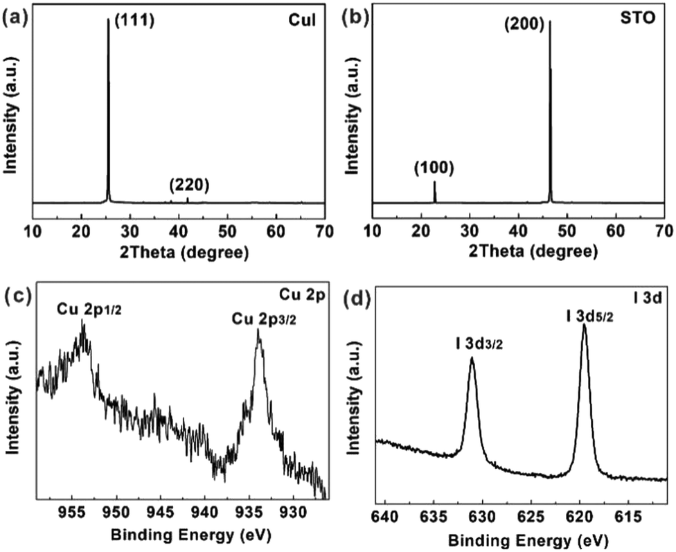 | ||
| Fig. 2 (a) and (b) XRD patterns of CuI and STO. (c) and (d) XPS spectra of the CuI film, (c) Cu 2p and (d) I 3d spectrum. | ||
Furthermore, the UV-vis absorption spectrum of the CuI film and STO wafer was recorded to investigate their optical property, respectively. As displayed in Fig. 3(a), the sharp absorption edge of the CuI film is at around 410 nm. And the optical bandgap can be estimated to be 3.0 eV by the Tauc plot using the UV-vis absorbance spectrum in Fig. 3(b). Meanwhile, the obvious absorption edge of the STO wafer is at around 400 nm in Fig. 3(c), and the corresponding bandgap could be calculated to be 3.1 eV, as seen in Fig. 3(d). Due to their approximate absorption edge and considerable bandgap width, the CuI/STO device may have strong coupling and unique photoelectric properties. The optical transmissivities of the obtained experimental samples are studied before the PD construction, and the corresponding results are displayed in Fig. 3(e). Both the CuI film and the STO wafer have good transparency in the visible region. The CuI film shows an obvious transmittance decline at about 400 nm, and then a gradual transmittance decline from 400 to 200 nm. Meanwhile, the STO film shows a sharp transmittance cut-off at about 400 nm. The CuI and STO films both maintain an average transmittance of 70% in the visible light region (400–760 nm) owing to the transparent crystal structure and the proper bandgap. Furthermore, the composite CuI/STO film has a high transmittance of >70% in the visible light range, and is opaque to ultraviolet radiation, with a sharp transmittance cut-off at about 400 nm. The light transmittance decreases sharply in the UV range, blocking 99.9% UV (200–385 nm) radiation. Fig. 3(f) displays the transmittance of the CuI/STO device photograph, which provides a clear observation of the PD transparency. The CuI/STO PD exhibits a visible light transparency of >70%, and the corresponding printed photograph can be distinguished evidently under the PD. These results are comparable to related transparent UV filters in previous literature.27–29 Therefore, the CuI/STO device has a high visible light transparency (>70%) and a high UV shielding (>99.9%).
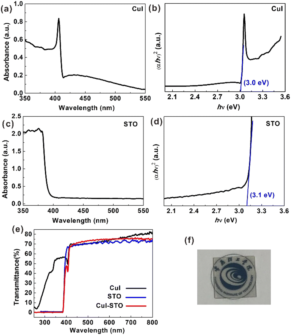 | ||
| Fig. 3 (a)–(d) UV-vis absorption spectrum of the CuI film (a) and STO wafer (c), and Tauc plot of the CuI film (b) and STO wafer (d) obtained from its absorbance spectrum, respectively. (e) The transmittance curves of the CuI film, the STO wafer and the CuI/STO film, respectively. (f) The photograph of the CuI/STO device on printed patterns. | ||
To investigate the photoelectric performance and self-powered features of the CuI-based device, the p–n heterojunction between the p-CuI film and the n-STO film was constructed via a simple vacuum thermal evaporation method. Two small indium grains were bladed onto the CuI and STO film as electrodes to form the heterojunction devices. The planar p-CuI/n-GaN PDs were constructed, as schematically described in Fig. 4(a). The performance of the as-fabricated device was measured by a two-probe technique in the atmospheric environment at room temperature. To quantitatively characterize the performance of the CuI/STO PD, Fig. 4(b) exhibits the current voltage curve (I–V) of this device in the dark and under 400 nm light irradiation in a logarithmic plot. And the nonsymmetrical I–V curve of the CuI/STO PD in the dark indicates the rectifying behavior from the p–n junction. It is observed clearly that the photocurrent could reach up to 31 nA at 5 V under 400 nm light irradiation, which is slightly higher than the photocurrent (25 nA) at −5 V. Furthermore, the photocurrents of this device are as high as 20![[thin space (1/6-em)]](https://www.rsc.org/images/entities/char_2009.gif) 000 times and 5000 times that of the dark current (1.5 pA) at 5 V and dark current (5.1 pA) at −5 V, respectively. In particular, an obvious shift of the I–V curve reveals the generation of an open-circuit voltage (0.5 V) upon 400 nm light irradiation. It is noteworthy that the great difference between the dark and photo current at zero bias reveals the excellent self-powered behaviors of this PD. In other words, upon 400 nm light irradiation, a large number of electron–hole pairs will be produced and separated. The built-in electric field generated by the heterojunction acts as the driving force, and the holes transfer from n-type STO to p-type CuI and electrons transport in the opposite direction. The high quality of the interface between CuI and STO was favourable to form the p–n heterojunction.
000 times and 5000 times that of the dark current (1.5 pA) at 5 V and dark current (5.1 pA) at −5 V, respectively. In particular, an obvious shift of the I–V curve reveals the generation of an open-circuit voltage (0.5 V) upon 400 nm light irradiation. It is noteworthy that the great difference between the dark and photo current at zero bias reveals the excellent self-powered behaviors of this PD. In other words, upon 400 nm light irradiation, a large number of electron–hole pairs will be produced and separated. The built-in electric field generated by the heterojunction acts as the driving force, and the holes transfer from n-type STO to p-type CuI and electrons transport in the opposite direction. The high quality of the interface between CuI and STO was favourable to form the p–n heterojunction.
 | ||
| Fig. 4 (a) Schematic illustration of the CuI/STO device structure. (b)–(d) I–V curves of the CuI/STO device, pure CuI device and pure STO device, respectively. | ||
To explain the origin of the self-powered behaviour, the I–V features of pure CuI and STO PDs are shown in Fig. 4(c) and (d), respectively. The nearly symmetrical I–V curves suggest that the junction between In electrodes and CuI (STO) is unable to produce the self-powered behavior owing to a narrow depletion area from a relatively low barrier height. Thereby it is proved that this prominent self-powered feature mainly results from the p-CuI/n-STO heterojunction between CuI and STO. As displayed in Fig. 4(c), the I–V curve indicates that the CuI film exhibits a high conductivity; however, the CuI PD has no obvious photo-response features. The current of the CuI device reaches the mA level. As exhibited in Fig. 4(d), the photocurrent of the pure STO device reaches 0.4 nA at 5 V, which is 1200 times that of the dark current (0.33 pA) under 400 nm light illumination, which demonstrates that the STO PD exhibits a good photo-response. In particular, the CuI is a p-type semiconductor and has a high hole mobility. Meanwhile, the STO is an n-type semiconductor and has a high electron mobility. So, the built-in electric field acts as the driving force to separate the electrons and holes upon 400 nm light irradiation, leading to a relatively large photocurrent. These results indicate that the CuI/STO devices not only exhibit enhanced photocurrent, but also have a potential self-powered ability.
To further explore the photoelectric features, the current–time (I–t) curves of the CuI/STO PD at −0.5 V and 0.5 V were measured separately. The results are exhibited in Fig. 5(a) and (b), respectively. It is found that the CuI/STO device shows a reproducible photo-response upon 400 nm light illumination at 0.5 V and −0.5 V, respectively. The current of the PD increases rapidly to 60 pA and decreases rapidly to 0.06 pA as the light is switched on and off at −0.5 V, while the current of the PD quickly increases to 4 nA and quickly declines to 0.1 pA when the 400 nm light is turned on and off at 0.5 V. The on/off ratio is described as the ratio of photocurrent to dark current (Iph/Id) of a device. By comparing the data, it is clear that the CuI/STO device at 0.5 V exhibits higher photocurrent (4 nA) and larger on–off ratio (4 × 10⁴) than the 0.06 nA and 1 × 10³ at −0.5 V, respectively. Due to its 0.5 V open-circuit voltage, the CuI/STO device shows evidently different properties at −0.5 V and 0.5 V separately. As shown in Fig. 5(c), the currents of the STO and CuI/STO PDs rise rapidly to 0.4 and 24.0 nA, and then decline quickly to 1.0 and 3.0 pA as the light is switched on and off separately. And the corresponding on–off ratios are estimated to be 400 and 8000, respectively. Therefore, the CuI/STO device presents much larger photocurrent and much higher on–off ratio than the pure STO device. This may be explained due to the high conductivity and enhanced light absorption of the CuI film. These results confirm that this CuI/STO device presents enhanced photocurrent and may operate at different biases to realize multifunctional detection when the p–n heterojunctions were formed successfully at the interface.
 | ||
| Fig. 5 (a) and (b) I–t curves of the CuI/STO device at different bias voltages, respectively. (c) and (d) Comparison of I–t curves (c) and the responsivity (d) between CuI/STO and STO devices at 5 V, respectively. | ||
The spectral responsivity (Rλ) and specific detectivity (D*) are examined to evaluate and compare the performance of these devices at 5 V bias voltage. The responsivity can be described as the photocurrent per unit of incident light power, which indicates the efficiency of a device in detecting the light signals. The specific detectivity (D*) defines the ability of a detector to respond to weak light signals in a noise environment. Herein the major contributor originates from the shot noise in the dark current. The responsivity and detectivity of a detector can be expressed as the following equations:
| Rλ = (Iph − Id)/(Pλ·S) | (1) |
| D* = Rλ/(2eId/S)1/2 | (2) |
The response speed and repeatability are significant parameters to evaluate the performance of a detector. Fig. 6(a) exhibits the I–t curve of the CuI/STO PD at 0 V under a periodic 400 nm light irradiation. The I–t curve presents good stability and a fast response without noticeable delay. For the CuI/STO PD, the photocurrent retains good repeatability at 0 V. This indicates that the built-in electric field could operate efficiently without an external voltage. The photocurrent of this PD increases rapidly to 2.5 nA and then quickly decreases to 0.36 pA as the 400 nm light is switched on and off. And the corresponding on–off ratio of the CuI/STO device is calculated to be about 7000. A rapid measurement equipment is applied to calculate the accurate time of this CuI/STO PD. The normalized curves of the response as a function of time at zero bias are displayed in Fig. 6(b). The rise and fall times of the CuI/STO PD are measured to be 0.6 and 3.3 ms at zero bias, respectively. The excellent self-powered features mainly originate from the p–n junction, which produces a built-in electrical field and separates the photo-generated carriers. Therefore, the CuI/STO device exhibits good repeatability, high on/off ratio (7000) and fast speed (0.6/3.3 ms) at zero bias, indicating its great potential for developing microscale photodetectors.
 | ||
| Fig. 6 (a) I–t curves of the CuI/STO device at 0 V. (b) The normalized single pulse response of the CuI/STO device at 0 V. (c) The responsivity and the detectivity of the CuI/STO device at 0 V, respectively. (d) The schematic energy band diagram of the CuI/STO device. | ||
Fig. 6(c) displays the responsivity and the detectivity of the CuI/STO PD with excitation wavelength in the range of 600–300 nm at 0 V, respectively. As seen in Fig. 6(c), the CuI/STO device has a maximum responsivity of 22.15 μA W−1 at 390 nm, and the responsivity rapidly increases from 420 nm (0.78 μA W−1) to 390 nm (22.15 μA W−1) and then dramatically decreases at 360 nm (0.025 μA W−1) ranging from 600 to 300 nm. The responsivity of the CuI/STO film device is relatively low, and it can be further improved by reducing the effective irradiation area. The detectivity (D*) also exhibits a similar trend to the responsivity, and has a maximum value of 2.26 × 10¹⁰ Jones. The detectivity rises quickly from 420 nm (0.08 × 10¹⁰ Jones) to 390 nm (2.26 × 10¹⁰ Jones) and then falls quickly at 360 nm (0.02 × 10¹⁰ Jones) in the range of 600–300 nm. The cut-off wavelength, defined as the ratio of the maximum to the natural constant (e ≈ 2.718), occurs at 375 and 405 nm, respectively. That is, the CuI/STO device has a narrowed photo-response spectrum (405–375 nm). The full width at half maximum (FWHM) of the CuI/STO device is about 27 nm at zero bias. Recently, the GaN/MoO3 heterojunction and the CuGaTe2/Si p–n junction PDs all demonstrate self-powered characteristics and narrowband response because of nonequilibrium photogenerated carrier transport in the p–n junction region.30–33 In addition, it can be found through comparison that the photo-response curve of the CuI/STO device is steeper (<390 nm) than that of the STO device, and the photo-response curve of the CuI/STO device at 0 V is much steeper (<390 nm) than that of the device at 5 V. The CuI film deposited on the STO film can decrease the light penetration distance. Meanwhile, part of the photo-generated electrons of STO may be quenched by the holes of CuI upon light irradiation (<390 nm). With the decrease of applied bias, the photo-generated carrier collection efficiency by the built-in electric field will be further weakened in the short wavelength range. The wavelength of 400 nm is the dividing point between visible light and UV light. Therefore, the CuI/STO device has excellent self-powered performance, and is a purple-light sensitive (375–405 nm) detector, and could realize effectively power-free, filter-free and UV-shielding photodetectors.
To investigate the self-powered mechanism for the CuI/STO PD, the energy levels of p-CuI and n-STO are exhibited in Fig. 6(d). Due to the formation of the p–n heterojunction, the CuI/STO device demonstrates excellent self-powered characteristics. Under 400 nm light illumination, the pure STO device displays high photo-response at 390 nm, and the CuI/STO PD also exhibits high performance under 390 light irradiation, indicating that STO plays a major role in the photoelectric performance of the CuI/STO PD. Therefore, the STO wafer is the main carrier transport channel. In addition, the electron affinities of CuI and STO are regarded as 3.3 and 3.6 eV, while their band gaps are 3.0 and 3.1 eV, respectively.25,34 After the CuI covering, the interface between CuI and STO is bonded closely, permitting good charge collection. Upon 390 nm light irradiation, photo-generated carriers will be quickly separated by the built-in electric field at the interface of CuI and STO. According to the band diagram, the CuI and STO consist of a typical Type II heterojunction. The electrons in the CuI conduction band will transfer to the STO side, and the holes in STO will move to the CuI valence band, yielding a stable photocurrent. Photo-generated electron–hole pairs passing through the heterojunction barrier will be collected by the corresponding electrodes. The close interface contact of this planar photodetector structure makes the carriers quickly move and reach the corresponding electrodes. This is conducive to significant enhancement of photocurrent. At the same time, the energy band diagram of the CuI/STO interface exhibits the valence band and conduction band offsets. These offsets provide a large barrier for the diffusion induced transport of holes and electrons. This explains the reason for the low forward current in the dark.
With the increase of the light penetration distance, the number of carriers in the crystal exponentially decreases. The low extinction coefficient of the STO crystal in the long wavelength indicates a wide region. However, the high extinction coefficient in the short wavelength reveals that the photo-generated carrier shows a narrow region near the irradiated side. Generally speaking, the narrowband PD is related closely to light penetration distance and the carrier diffusion length in the whole spectral region. The carrier diffusion length is affected by the thickness of the film and the utilized bias for PDs. Due to the large thickness of the STO wafer, this CuI/STO PD displays relatively weak photoresponse in the short wavelength region. And the surface-carrier recombination generated from CuI can also decrease the photoresponse under the light irradiation. Moreover, the carrier collection efficiency will be weakened in the short wavelength range at the electrode with the decrease of the utilized bias. Self-powered PDs can work without an external power source, which is appealing for their miniaturization, portability and integration.35,36 Self-powered narrowband PDs can detect specific wavelengths without needing an optical filter, and show high noise immunity and high potential for secure optical communication systems and high quality biological imaging.30,31,37,38 In addition, UV shielding is highly desired to protect against the ultraviolet irradiation and the increasing light pollution.39 Therefore, this power-free, filter-free and UV-free PD shows considerable promise in real-life applications.
Conclusions
In summary, the heterojunction film between p-CuI and n-SrTiO3 was prepared by a simple vacuum thermal evaporation. Compared with the STO device, the CuI/STO device exhibits markedly enhanced photocurrents. Furthermore, the CuI/STO device presents high on/off ratio (7 × 10³) and fast response speed (0.6/3.3 ms) at 0 V at 400 nm. In particular, the CuI/STO device shows a great narrowband photoresponse (FWHM ∼ 27 nm) at zero bias. More importantly, the CuI/STO device demonstrates a transparency of 70% over the entire visible light region and blocks 99.9% UV light (200–385 nm). This work provides an effective strategy to realize power-free, filter-free and UV-free photodetectors for many special applications.Author contributions
The manuscript was written through contributions of all authors. All authors have given approval to the final version of the manuscript. Yong Zhang: conceptualization, formal analysis, writing – original draft, and supervision. Hui Liu: validation, investigation, formal analysis, and resources. Shuai Liu: validation, formal analysis, investigation, and resources. Qian Gong: writing – review & editing, and resources. Yushen Liu: writing – review & editing, resources, and supervision. Dan Tian: writing – review & editing, resources, and supervision. Lixing Kang: writing – review & editing, resources, and supervision.Conflicts of interest
There are no conflicts to declare.Acknowledgements
This work was supported by China Postdoctoral Science Foundation (2022M712322), High level Scientific Research Cultivation Project of Hubei Minzu University (No. PY22001), National Natural Science Foundation of China (No. 21971113, 22175094, 62174016, and 52272136), Natural Science Foundation of Jiangsu Higher Education Institutions (20KJA150001) and Jiangsu Independent Innovation Fund Project of Agricultural Science and Technology (CX(21)3163), Jiangsu Natural Science Foundation (BK20221402). The authors are grateful for the technical support for Nano-X from Suzhou Institute of Nano-Tech and Nano-Bionics, Chinese Academy of Sciences (SINANO).Notes and references
- Y. Zhang, Y. Ma, Y. Wang, X. Zhang, C. Zuo, L. Shen and L. Ding, Adv. Mater., 2021, 33, 2006691 CrossRef CAS.
- Q. Qiu and Z. Huang, Adv. Mater., 2021, 33, 2008126 CrossRef CAS.
- Y. Zhang, X. Zhao, J. Chen, S. Li, W. Yang and X. Fang, Adv. Funct. Mater., 2020, 30, 1907650 CrossRef CAS.
- Y. Zhang, S. Li, Z. Li, H. Liu, X. Liu, J. Chen and X. Fang, Nano Lett., 2021, 21, 382–388 CrossRef CAS PubMed.
- Y. Zhang, F. Cao, S. Li, X. Liu, L. Kang, L. Wu and X. Fang, J. Mater. Sci. Technol., 2022, 129, 108–114 CrossRef.
- X. Du, W. Tian, J. Pan, B. Hui, J. Sun, K. Zhang and Y. Xia, Nano Energy, 2022, 92, 106743 CrossRef.
- X. Hu, X. Li, G. Li, T. Ji, F. Ai, J. Wu, E. Ha and J. Hu, Adv. Funct. Mater., 2021, 31, 2011284 CrossRef CAS.
- M. Al Fattah, A. Khan, H. Anabestani, M. Rana, S. Rassel, J. Therrien and D. Ban, Nanoscale, 2021, 13, 15526–15551 RSC.
- J. Chen, W. Ouyang, W. Yang, J. He and X. Fang, Adv. Funct. Mater., 2020, 30, 1909909 CrossRef CAS.
- Y. Zhang and W. Song, J. Mater. Chem. C, 2021, 9, 4799–4807 RSC.
- Y. Zhang, W. Liu, Y. Liu, C. Wang, G. Zhu and W. Song, J. Mater. Chem. C, 2021, 9, 15654–15661 RSC.
- H. Wang and D. Kim, Chem. Soc. Rev., 2017, 46, 5204–5236 RSC.
- E. Cicek, R. McClintock, C. Cho, B. Rahnema and M. Razeghi, Appl. Phys. Lett., 2013, 103, 191108 CrossRef.
- A. Sobhani, M. Knight, Y. Wang, B. Zheng, N. King, L. Brown, Z. Fang, P. Nordlander and N. Halas, Nat. Commun., 2013, 4, 1643 CrossRef PubMed.
- F. Cao, J. Chen, D. Yu, S. Wang, X. Xu, J. Liu, Z. Han, B. Huang, Y. Gu, K. Choy and H. Zeng, Adv. Mater., 2020, 32, 1905362 CrossRef CAS PubMed.
- Y. Higashi, K. Kim, H. Jeon and M. Ichikawa, J. Appl. Phys., 2010, 108, 034502 CrossRef.
- A. Armin, R. Jansen-van Vuuren, N. Kopidakis, P. Burn and P. Meredith, Nat. Commun., 2015, 6, 6343 CrossRef CAS.
- J. Li, J. Wang, J. Ma, H. Shen, L. Li, X. Duan and D. Li, Nat. Commun., 2019, 10, 806 CrossRef.
- J. Xue, Z. Zhu, X. Xu, Y. Gu, S. Wang, L. Xu, Y. Zou, J. Song, H. Zeng and Q. Chen, Nano Lett., 2018, 18, 7628–7634 CrossRef CAS PubMed.
- D. Walker, H. Vollmer-Snarr and C. Eberting, J. Am. Acad. Dermatol., 2012, 66, 130–135 CrossRef PubMed.
- J. Lu, B. Jiang, F. Hsiao, Y. Peng, Y. Su, Y. Lin, T. Tsai, M. Shiu, C. Lin, Y. Fang and C. Chen, Chem. Eng. J., 2022, 437, 135327 CrossRef CAS.
- N. Subramani, S. Kasargod Nagaraj, S. Shivanna and H. Siddaramaiah, Macromolecules, 2016, 49, 2791–2801 CrossRef CAS.
- Z. Xie, Q. Du, Y. Wu, X. Hao and C. Liu, J. Mater. Chem. C, 2016, 4, 9879–9886 RSC.
- J. Xu, H. Nagasawa, M. Kanezashi and T. Tsuru, ACS Appl. Mater. Interfaces, 2018, 10, 42657–42665 CrossRef CAS.
- Y. Zhang, S. Li, W. Yang, M. Joshi and X. Fang, J. Phys. Chem. Lett., 2019, 10, 2400–2407 CrossRef CAS PubMed.
- Y. Zhang, X. Xu and X. Fang, InfoMat, 2019, 1, 542–551 CrossRef CAS.
- D. Chen, W. Sun, C. Qian, A. Wong, L. Reyes and G. Ozin, Adv. Opt. Mater., 2017, 5, 1700237 CrossRef.
- J. Zhang, W. Lei, J. Chen, D. Liu, B. Tang, J. Li and X. Wang, Polymer, 2018, 148, 101–108 CrossRef CAS.
- X. Zhang, W. Liu, D. Yang and X. Qiu, Adv. Funct. Mater., 2019, 29, 1806912 CrossRef.
- Y. Guo, W. Song, Q. Liu, Y. Sun, Z. Chen, X. He, Q. Zeng, X. Luo, R. Zhang and S. Li, J. Mater. Chem. C, 2022, 10, 5116–5123 RSC.
- L. Wang, Z. Li, M. Li, S. Li, Y. Lu, N. Qi, J. Zhang, C. Xie, C. Wu and L. Luo, ACS Appl. Mater. Interfaces, 2020, 12, 21845–21853 CrossRef CAS.
- J. Wang, S. Xiao, W. Qian, K. Zhang, J. Yu, X. Xu, G. Wang, S. Zheng and S. Yang, Adv. Mater., 2020, 33, 2005557 CrossRef PubMed.
- Y. Hou, C. Wu, X. Huang, D. Yang, T. Ye, J. Yoon, R. Sriramdas, K. Wang and S. Priy, Adv. Funct. Mater., 2020, 31, 2007016 CrossRef.
- W. Yang, Y. Zhang, Y. Zhang, W. Deng and X. Fang, Adv. Funct. Mater., 2019, 29, 1905923 CrossRef CAS.
- Z. Zhang, Y. Ning and X. Fang, J. Mater. Chem. C, 2019, 7, 223–229 RSC.
- Y. Chen, L. Su, M. Jiang and X. Fang, J. Mater. Sci. Technol., 2022, 105, 259–265 CrossRef.
- K. Li, Y. Lu, X. Yang, L. Fu, J. He, X. Lin, J. Zheng, S. Lu, C. Chen and J. Tang, InfoMat, 2021, 3, 1145–1153 CrossRef CAS.
- W. Cheng, W. Tian, F. Cao and L. Li, InfoMat, 2022, e12348 CAS.
- X. Cui, J. Chen, W. Wu, Y. Liu, H. Li, Z. Xu and Y. Zhu, Nano Energy, 2022, 95, 107022 CrossRef CAS.
Footnotes |
| † Electronic supplementary information (ESI) available. See DOI: https://doi.org/10.1039/d2tc04294k |
| ‡ These authors contributed equally. |
| This journal is © The Royal Society of Chemistry 2023 |