
Efficiency boosting in Sb2(S,Se)3 solar cells enabled by tailoring bandgap gradient via a hybrid growth method†
Yazi
Wang‡
a,
Seunghwan
Ji‡
a,
Choongman
Moon
a,
Jinwoo
Chu
a,
Hee Joon
Jung
 *b and
Byungha
Shin
*a
*b and
Byungha
Shin
*a
aDepartment of Materials Science and Engineering, Korea Advanced Institute of Science and Technology (KAIST), Daejeon 34141, Republic of Korea. E-mail: byungha@kaist.ac.kr
bKorea Research Institute of Standards and Science (KRISS), Daejeon 34113, Republic of Korea. E-mail: hjjung@kriss.re.kr
First published on 11th October 2023
Abstract
Antimony selenosulfide (Sb2(S,Se)3) solar technology has garnered widespread interest in recent years due to its exceptional photovoltaic properties and excellent stability. The hydrothermal deposition method has enabled cell efficiencies of over 10% in state-of-the-art Sb2(S,Se)3 solar cells. Nevertheless, issues arising from the hydrothermal method, such as the formation of an inappropriate bandgap gradient during film growth and the loss of S and Se during the annealing process, remain unresolved. To address these challenges, we developed a hybrid growth method with a specific emphasis on optimizing the unfavorable bandgap gradient. This method consists of two stages: the first stage involves hydrothermal deposition, while the second stage employs vapor transport deposition. By controlling the second-stage process, two types of optimized bandgap gradients have been achieved. As a result, the short-circuit current density (Jsc) and fill factor (FF) of Sb2(S,Se)3 solar cells with a superstrate configuration of Glass/Fluorine-doped Tin Oxide/CdS/Sb2(S,Se)3/Poly(triaryl amine)/Au were significantly improved, resulting in a promising efficiency approaching 8%. The enhanced Jsc and FF can be attributed to the tailored bandgap gradient of the Sb2(S,Se)3 film fabricated using the hybrid method. This work presents a viable approach to enhance the device performance of Sb2(S,Se)3 solar cells and sheds new light on the fabrication of high-performance Sb2(S,Se)3-based photovoltaic devices.
Introduction
In recent years, antimony selenosulfide (Sb2(SxSe1−x)3, 0 < x < 1) has experienced a surge of interest as a promising photovoltaic material due to its superior optoelectrical properties, such as a strong light-absorbing capability and a tunable bandgap ranging from 1.1 to 1.7 eV.1–5 Notably, the performances of recently reported Sb2(S,Se)3 solar cells have gradually improved, with the record power conversion efficiencies (PCEs) exceeding 10%,6–8 demonstrating their potential for practical applications. However, despite these advancements, the current champion efficiency achieved by Sb2(S,Se)3 solar cells still significantly lags behind that of other well-established chalcogenide-based solar cells, such as CdTe (22.1%)9 and Cu(In,Ga)Se2 (CIGS) (23.35%).10 Researchers have been exploring various strategies to enhance the performance of Sb2(S,Se)3 solar cells.Bandgap engineering has proven to be a practical approach for achieving high photovoltaic performance in tunable bandgap solar cells, such as CIGS,11–16 and Cu2ZnSn(S,Se)4![[thin space (1/6-em)]](https://www.rsc.org/images/entities/char_2009.gif) 17–21 solar cells. For example, high-performance CIGS solar cells often employ a double-graded bandgap profile, featuring a narrower bandgap in the middle of the absorber layer and wider bandgaps at the front and back sides. The front grading enhances the open-circuit voltage (Voc),22,23 while the back grading facilitates carrier transport and suppresses interface recombination at the back contact.12 This optimization strategy significantly improves device performance. Similarly, researchers have recognized the potential of achieving a favorable bandgap gradient in Sb2(S,Se)3 solar cells by tuning the S/Se ratio, leveraging the isomorphic crystal structures of Sb2Se3 and Sb2S3.24–26 Various approaches have been explored to enhance the photovoltaic performance of Sb2(S,Se)3 solar cells. For instance, Li et al. achieved a V-shaped bandgap grading of Sb2(S,Se)3 film through a dual-source vapor transport deposition process, leading to enhanced Voc and short-circuit current density (Jsc), and a cell efficiency of 7.27%.27 Liu and co-workers utilized a co-sublimation technique, varying the molar ratio of Sb2Se3 and Sb2S3 sources to fabricate a V-shaped graded bandgap. Their work achieved a record PCE of 9.02% for Cd-free Sb-based solar cells.28 Zhao et al. proposed a solution post-treatment technique (SPT) to control the bandgap grading of Sb2(S,Se)3 deposited using the hydrothermal method.8 By using alkaline metal fluoride-assisted SPT, they successfully generated a shallow bandgap gradient within the Sb2(S,Se)3 film, resulting in a favorable energy band structure promoting efficient charge carrier transfer. This approach led to significant improvements in Jsc and fill factor (FF), ultimately achieving the highest PCE of 10.7% among antimony chalcogenide solar cells.
17–21 solar cells. For example, high-performance CIGS solar cells often employ a double-graded bandgap profile, featuring a narrower bandgap in the middle of the absorber layer and wider bandgaps at the front and back sides. The front grading enhances the open-circuit voltage (Voc),22,23 while the back grading facilitates carrier transport and suppresses interface recombination at the back contact.12 This optimization strategy significantly improves device performance. Similarly, researchers have recognized the potential of achieving a favorable bandgap gradient in Sb2(S,Se)3 solar cells by tuning the S/Se ratio, leveraging the isomorphic crystal structures of Sb2Se3 and Sb2S3.24–26 Various approaches have been explored to enhance the photovoltaic performance of Sb2(S,Se)3 solar cells. For instance, Li et al. achieved a V-shaped bandgap grading of Sb2(S,Se)3 film through a dual-source vapor transport deposition process, leading to enhanced Voc and short-circuit current density (Jsc), and a cell efficiency of 7.27%.27 Liu and co-workers utilized a co-sublimation technique, varying the molar ratio of Sb2Se3 and Sb2S3 sources to fabricate a V-shaped graded bandgap. Their work achieved a record PCE of 9.02% for Cd-free Sb-based solar cells.28 Zhao et al. proposed a solution post-treatment technique (SPT) to control the bandgap grading of Sb2(S,Se)3 deposited using the hydrothermal method.8 By using alkaline metal fluoride-assisted SPT, they successfully generated a shallow bandgap gradient within the Sb2(S,Se)3 film, resulting in a favorable energy band structure promoting efficient charge carrier transfer. This approach led to significant improvements in Jsc and fill factor (FF), ultimately achieving the highest PCE of 10.7% among antimony chalcogenide solar cells.
The majority of recently reported high-efficiency Sb2(S,Se)3 solar cells are fabricated using a facile hydrothermal deposition method, which offers advantages such as low-temperature processing, high-quality thin film, and high reproducibility.6,29,30 However, this method is not without drawbacks. One commonly observed issue is a non-uniform distribution of S and Se in a growing Sb2(S,Se)3 film during the synthesis process. As the growth progresses, the Se content decreases while the S content increases, leading to a bandgap gradient from the S-rich surface (wider bandgap) to the Se-rich bottom (narrower bandgap). This compositional distribution hampers hole transport in the Sb2(S,Se)3 absorber layer, particularly in the superstrate configuration, and limits further improvement in cell efficiency.8 Another recently identified concern with the hydrothermal method is the loss of S and Se from the Sb2(S,Se)3 film in the subsequent annealing process for crystallization.31 This loss results in volume shrinkage and the formation of pinholes within the Sb2(S,Se)3, significantly impeding charge transfer and degrading the photovoltaic performance of Sb2(S,Se)3 solar cells. Therefore, it is crucial to adopt a comprehensive strategy that addresses the inappropriate bandgap gradient and simultaneously mitigates the loss of elements.
To address the limitations of the hydrothermal method, we developed a hybrid growth method to prepare Sb2(S,Se)3 absorber layers with an optimized bandgap gradient. Our approach involves a two-step process, starting with the first-stage hydrothermal deposition process, followed by the second-stage process using the vapor deposition transport (VTD) method. By combining these techniques, we aimed to overcome the challenges related to the bandgap gradient and element loss. In the VTD process, amorphous Sb2(S,Se)3 thin films from the hydrothermal process were annealed under a Se-rich atmosphere created by the evaporation of Se-containing powder (Sb2Se3 and/or pure Se). This process allowed for tailoring the surface S-rich bandgap gradient of Sb2(S,Se)3 while simultaneously preventing the loss of Se. We adopted superstrate Sb2(S,Se)3 solar cells in this work, with a cell configuration of glass/fluorine-doped tin oxide (FTO)/CdS/Sb2(S,Se)3/Poly(triaryl amine)(PTAA)/Au. By carefully controlling the second-stage VTD process, we optimized the bandgap grading of the Sb2(S,Se)3 absorber layers in two ways. In both cases, a Se-rich surface was formed, which improved hole transport and enhanced the efficiency of charge carrier collection. As a result, the Jsc and FF of Sb2(S,Se)3 solar cells fabricated using the hybrid method were notably improved compared to the reference devices prepared solely using the first-stage hydrothermal method, eventually yielding a cell efficiency approaching 8%.
Experimental section
First-stage process with hydrothermal deposition method
The Sb2(S,Se)3 films were fabricated using a hydrothermal deposition method, employing potassium antimonyl tartrate trihydrate (K2Sb2(C4H2O6)2·3H2O), sodium thiosulfate pentahydrate (Na2S2O3·5H2O), and selenourea (SeC(NH2)2) as sources for Sb, S, and Se, respectively. Initially, 14.2 mM K2Sb2(C4H2O6)2·3H2O and 68.5 mM Na2S2O3·5H2O were mixed in 50 mL of deionized water and stirred until a homogenous liquid was obtained. Subsequently, 6.9 mM SeC(NH2)2 was added to the mixture and continuously stirred until a pale yellow clear precursor solution was formed. The as-prepared samples were placed into a Teflon container filled with the precursor solution, with the sample surfaces facing downwards. The Teflon container in the autoclave was then transferred to a dry cabinet oven and heated at 125 °C for 3.5 h. Afterward, the autoclave was allowed to cool to room temperature, and the samples were removed, rinsed with DI water, and dried with nitrogen. Note that all the parameters we provided for this process are optimized.Second-stage process with vapor deposition transport method
As-grown amorphous Sb2(S,Se)3 thin films were placed into a tube furnace with four separate heating zones designed for the vapor transport deposition process. Two types of Se-containing powder were chosen as evaporation sources: a mixed powder comprising 20 mg of Sb2Se3 and 5 mg of Se, or 20 mg of pure Se powder. During the process, the Se-containing source powders were evaporated at a temperature of 480 °C, while the substrate temperature was maintained at 300 °C, and the distance from the substrate to the source was kept at 15 cm. Once the process was completed, the tube was allowed to cool down naturally to reach room temperature, and then the samples were retrieved. It is important to highlight that the parameters we have presented for this process have all been fine-tuned for optimization.Device fabrication
Adopting the conventional superstrate Sb2(S,Se)3 solar cell structure (Glass/FTO/ETL/Sb2(S,Se)3/HTL/Au), CdS was selected as the electron transport layer (ETL) and fabricated using a chemical bath deposition (CBD) method. The as-deposited CdS layer was subsequently treated with CdCl2, and further details of this process can be found in our previous publications.32,33 For the hole transport layer (HTL), a solution of PTAA HTL was prepared by mixing 10 mg of PTAA, 8 μL of 4-tert-butylpyridine (tBP), and 17.5 μL of 170 mg mL−1 lithium bis(trifluoromethylsulphonyl)imide (LiTFSI) in a mixture of 500 μL toluene and 500 μL N-methyl-2-pyrrolidone (NMP). The PTAA solution was then spin-coated onto the Sb2(S,Se)3 films at a speed of 4500 rpm for 25 s. Finally, Au electrodes with a thickness of 100 nm were deposited using a thermal evaporation system. The active area of the device was 0.1125 cm2, as defined by a shadow mask.Material characterizations
The crystal structures of the Sb2(S,Se)3 films were analyzed using an X-ray diffractometer (SmartLab, Rigaku) with a Cu-Kα line as the X-ray source. The cross-sectional structural analyses of Sb2(S,Se)3 layers were conducted using transmission electron microscopy (TEM, Thermofisher Scientific Tecnai G2 F30) at 300 kV acceleration voltage and scanning electron microscopy (SEM, Hitachi SU5000). Bright-field TEM (BFTEM) was recorded from the center transmitted beam filtered by an objective aperture of 10 μm, and selected area diffraction (SAD) patterns were obtained using a SAD aperture with a diameter of 200 nm. The chemical maps were collected using Spectra 300 with scanning transmission electron microscopy – X-ray energy dispersive spectroscopy (STEM-EDS). The detailed settings were 150 pA probe current, 22.7 mrad convergence angle, and 0.9 srad X-ray collection solid angles from Super X EDS system (four Silicon Drift Detectors). Cross-section TEM samples were prepared using focused ion beam (FIB, FEI Helios NanoLab 650) operated at 30 kV Ga focused ion beam, and the sample surface was fine-cleaned using the low acceleration of 1 kV beam. The current density–voltage (J–V) characteristics were measured under simulated AM 1.5 (100 mW cm−2) illumination using a solar simulator (Oriel, Model 94043, Newport) with a source meter (Keithley, 2400). The dark J–V measurement was conducted solely using the source meter at room temperature. The external quantum efficiency (EQE) spectra of the devices were obtained using a solar cell quantum efficiency measurement system (QEX7). The elemental depth profiles of the Sb2(S,Se)3 thin films were determined using time-of-flight secondary ion mass spectrometry (TOF-SIMS, ION-TOF GmbH). The impedance spectra were acquired using a potentiostat/galvanostat (SP-150, Bio-Logic). The positions of the valence band maximum (VBM) were determined through ultraviolet photoelectron spectroscopy (UPS, Axis-Supra) measurement.
Results and discussion
Fabrication process and photovoltaic performance
Fig. 1 illustrates the fabrication process of superstrate Sb2(S,Se)3 solar cells. The as-grown Sb2(S,Se)3 films from the first-stage hydrothermal deposition process, which subsequently underwent annealing treatment for crystallization in a tube furnace filled with N2 at 350 °C for 10 minutes, are denoted as “HTD”, and the corresponding devices are also referred to by the same name. In contrast, the Sb2(S,Se)3 films fabricated using the two-stage deposition process, with the second stage employing a single Se source of Se powder or a mixed Se source of Sb2Se3 and Se powder, are labelled as “HTD + VTD (Se)” and “HTD + VTD (Sb2Se3 + Se)”, respectively. Further details on the process can be found in the experimental section.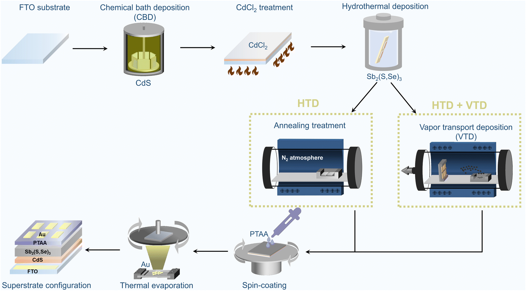 | ||
| Fig. 1 Schematic illustration of the fabrication process of superstrate-structured Sb2(S,Se)3 solar cells. (*HTD: hydrothermal deposition, *VTD: vapor transport deposition). | ||
The photovoltaic performance of the solar devices is presented in Fig. 2. The devices with the optimized two-stage process (HTD + VTD (Se) and HTD + VTD (Sb2Se3 + Se)) exhibited enhanced performance compared to the control device (HTD) (Fig. 2a–d). The improved performance primarily stems from the increased Jsc and FF. The photovoltaic parameters of champion cells from the control HTD samples with varying deposition time and the optimized HTD + VTD devices are summarized in Table 1. Note that 3.5 h represents the optimal deposition time for HTD samples, and all VTD processes were conducted under this condition. The thicknesses of the corresponding Sb2(S,Se)3 films are also included in Table 1. The nominal bandgaps of HTD, HTD + VTD (Se), and HTD + VTD (Sb2Se3 + Se) Sb2(S,Se)3 were estimated to be 1.53, 1.51 and 1.61 eV, respectively. These values were determined from the peak position of the first-order derivative of the EQE curve (see ESI Fig. S1†).34,35Fig. 2e displays the light current density–voltage (J–V) curves of the best-performing cells for each device. The changes in Jsc were further confirmed by the EQE spectra shown in Fig. 2f. The HTD + VTD (Se) sample exhibited an increase in Jsc, aligning with an amplified response within the 500–900 nm wavelength range. On the other hand, the HTD + VTD (Sb2Se3 + Se) device showed a slightly increased Jsc from an improved EQE response within the 500–750 nm range in spite of a reduced response in the range of 750–900 nm. In comparison to the control (HTD) sample, the HTD + VTD (Se) devices exhibited a slight decrease in Voc, while the HTD + VTD (Sb2Se3 + Se) samples showed a marginal increase. The change in Voc with the application of the second-stage VTD process can be assigned to the bandgap change of Sb2(S,Se)3 and the valence band offset (VBO) at the HTL(PTAA)/Sb2(S,Se)3 interface, as explained later. Additionally, it is noteworthy that both HTD + VTD (Se) and HTD + VTD (Sb2Se3 + Se) devices demonstrated a significant increase in FF. This improvement is consistent with a decrease in series resistance (RS) and an increase in shunt resistance (RSH) (See ESI Fig. S2†). Further details and a comprehensive analysis will be provided in the subsequent section.
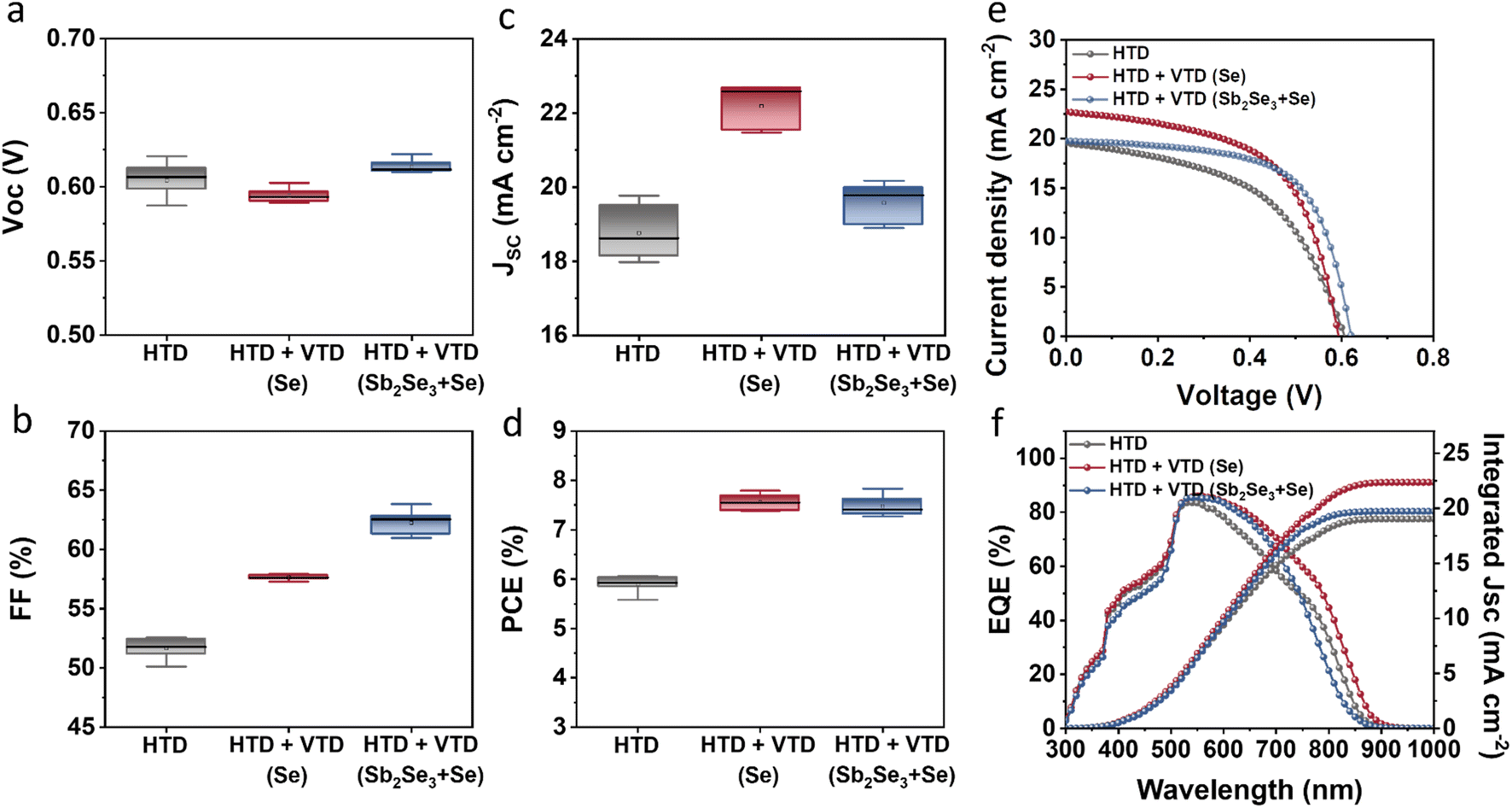 | ||
| Fig. 2 Device performance of HTD, HTD + VTD (Se), and HTD + VTD (Sb2Se3 + Se) Sb2(S,Se)3 solar cells: Statistical box plots of (a) Voc, (b) FF, (c) Jsc, (d) PCE, (e) J–V curves, and (f) EQE spectra. | ||
| Sample name | HTD duration time [h] | V oc [V] | J sc [mA cm−2] | FF [%] | PCE [%] | Thickness [nm] |
|---|---|---|---|---|---|---|
| HTD | 2 | 0.488 | 16.92 | 40.91 | 3.38 | 230 |
| HTD (optimized) | 3.5 | 0.607 | 19.54 | 51.12 | 6.06 | 350 |
| HTD | 5 | 0.617 | 19.98 | 40.62 | 5.01 | 590 |
| HTD (optimized) + VTD (Se) | 3.5 | 0.597 | 21.99 | 58.89 | 7.74 | 340 |
| HTD (optimized) + VTD (Sb2Se3 + Se) | 3.5 | 0.622 | 19.73 | 63.82 | 7.83 | 610 |
Evolution of energy band structures
To gain insights into the mechanism behind the enhanced photovoltaic performance achieved through the second-stage process, we conducted analysis on the crystal structure, elemental composition, and depth profiling of Sb2(S,Se)3 films. The examination of the crystalline structures by XRD (Fig. 3a) confirmed the successful synthesis of Sb2(S,Se)3 compounds, as evidenced by the presence of major peaks whose positions lie between the standard diffraction peaks of Sb2Se3 and Sb2S3. In the case of HTD + VTD (Se), no obvious peak shift or peak splitting was found, while a notable peak splitting was observed in the HTD + VTD (Sb2Se3 + Se), as represented by the (120) peak. The splitting of the peak suggests the formation of two regions with different anion compositions (S-rich region and Se-rich region)—presumably, Sb2(S,Se)3 layers with a higher Se content on the top surface during the second-stage process.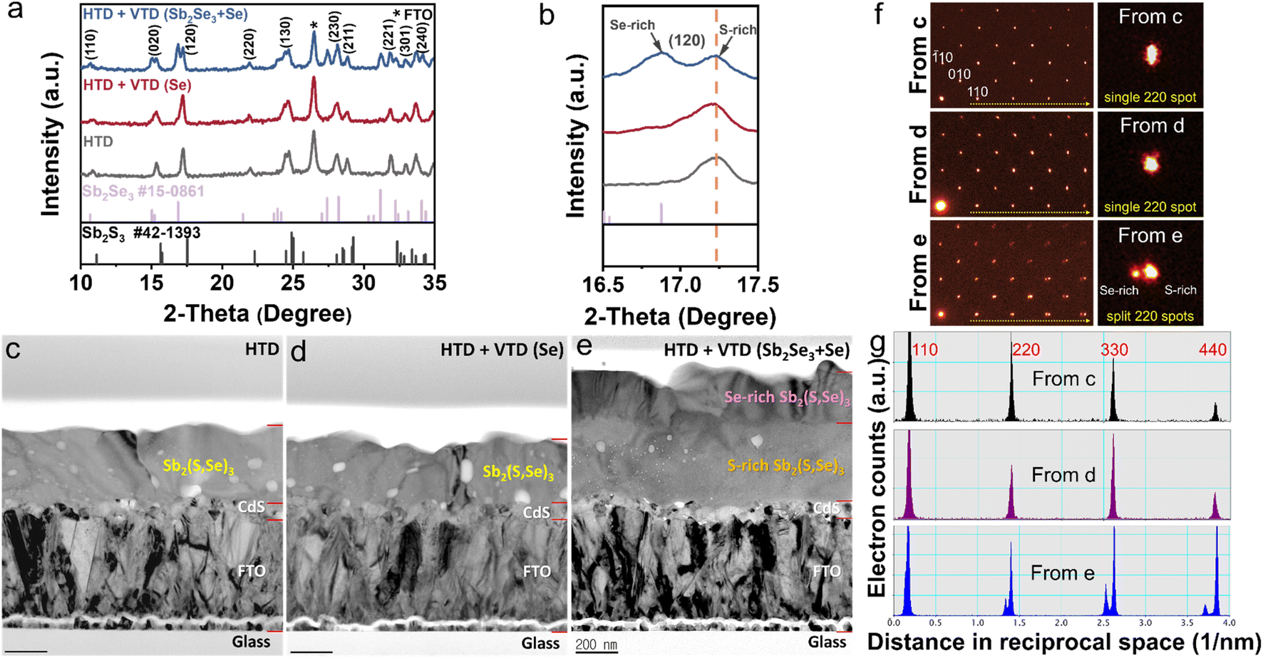 | ||
| Fig. 3 (a) XRD patterns and (b) enlarged patterns around (120) peak of the relative Sb2(S,Se)3 films. Cross-sectional BFTEM images of the corresponding Sb2(S,Se)3 films: (c) HTD, (d) HTD + VTD (Se), and (e) HTD + VTD (Sb2Se3 + Se). (f) SAD patterns on [001] zone axis from (c) (top left) (d) (middle left), and (e) (bottom left) with magnified 220 diffraction spots on the right column. It is worth noting that overall peak splits were observed only from the HTD + VTD (Sb2Se3 + Se). (g) Line profiles of hh0 type diffraction spots (yellow dotted arrows in (f)). | ||
Fig. 3c–e present bright-field TEM (BFTEM) images acquired using the smallest objective aperture (d = 10 μm). The mass-thickness contrast in the BFTEM is sensitive to mass, when a smaller objective aperture filters the center transmitted beam.36 In contrast to overall even contrast in Fig. 4c and 3d, the cross-sectional BFTEM in Fig. 3e exhibits two distinct layers with different contrast. The top layer with the darker contrast should have a slightly higher mass, which is Se-rich Sb2(S,Se)3, while the bottom layer with the lighter contrast corresponds to S-rich Sb2(S,Se)3, which is in line with the STEM-EDS mapping images (Fig. S3†). These pieces of evidence are consistent with our speculation from the XRD analysis. SAD patterns on the same [001] zone were acquired with a SAD aperture of 200 nm diameter, which is small enough to only examine the Sb2(S,Se)3. There are splits of diffraction spots in the SAD from HTD + VTD (Sb2Se3 + Se) film in Fig. 3f (bottom left) and Fig. S4c.† On the other hand, the other two samples display an array of a single set of diffraction spots in Fig. 3f (top and middle left) and Fig. S4a and b.† When we compare the enlarged 220 spots in the right column of Fig. 3f, the diffraction peak split of HTD + VTD (Sb2Se3 + Se) film is evident, consistent with the XRD result. Note that the SAD pattern from HTD + VTD (Sb2Se3 + Se) film was taken from an area including the interface of the top and bottom layers, indicating that the local crystallinity of the top layer follows that of the bottom layer epitaxially. Because the SAD on [001] zone-axis shows 100 and 010 spots in Fig. 3f and S4, we could determine lattice parameters a and b from the HTD only, and they are 11.3 and 11.5 Å, respectively. In the case of the HTD + VTD (Sb2Se3 + Se), there are two sets of a and b parameters due to the peak split, which are 11.7 and 11.8 Å from the Se-rich layer and 11.4 and 11.5 Å from the S-rich layer. Comparing the lattice parameters between the HTD and the HTD + VTD (Sb2Se3 + Se), we notice that the bottom S-rich layer of the HTD + VTD (Sb2Se3 + Se) is almost identical to the Sb2(S,Se)3 film from the HTD only, while the top Se-rich layer shows an expansion of 2.4% in a and 2.9% in b. Furthermore, the a (11.7 Å) and b (11.8 Å) values of the Se-rich top layer are very close to the reported values of a pure Sb2Se3 (a = 11.62 Å, b = 11.77 Å, c = 3.962 Å from Crystallography Open Database COD 9007437).37 The TEM analysis also revealed that the HTD + VTD (Sb2Se3 + Se) sample had a thicker absorber layer than the other samples, as anticipated, given that the Sb source was included in the VTD process. However, we note that the enhanced photovoltaic performance of the HTD + VTD (Sb2Se3 + Se) device does not stem from the increased thickness of the Sb2(S,Se)3 layer. This is evident from the significant decrease in the cell efficiency observed in the HTD sample deposited for 5 h (longer than the optimal deposition time of 3.5 h) but having a similar thickness to the optimized HTD + VTD (Sb2Se3 + Se) sample. Specifically, when compared to the HTD (3.5 h) (Optimized) sample, the HTD (5 h) counterpart exhibits inferior behavior, while the HTD (3.5 h) (Optimized) + VTD (Sb2Se3 + Se) device performs better, despite these two samples having comparable absorber layer thicknesses (see ESI Fig. S6 and S7†).
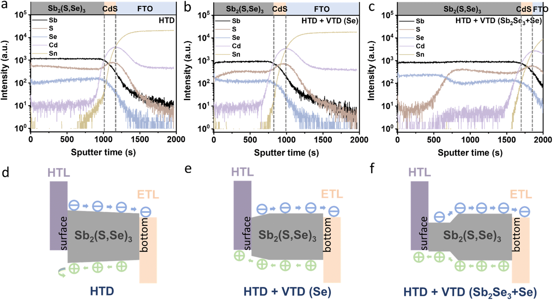 | ||
| Fig. 4 Depth profiling via TOF-SIMS of the Sb2(S,Se)3 films and energy band structures of the corresponding solar devices: (a and d) HTD, (b and e) HTD + VTD (Se), and (c and f) HTD + VTD (Sb2Se3 + Se). | ||
To investigate the elemental distribution within the Sb2(S,Se)3 layers, we performed depth profiling using TOF-SIMS (Fig. 4a–c). Consistent with previous findings, the incorporation rate of Se2− was found to be faster than that of S2−, resulting in an increasing S/Se ratio from the bottom to the top surface of the Sb2(S,Se)3 layers during the hydrothermal deposition process.38 In the HTD sample, a higher S/Se ratio was observed on the top surface, whereas the S/Se ratio decreased from the bottom to the surface of Sb2(S,Se)3 of the HTD + VTD (Se) and HTD + VTD (Sb2Se3 + Se) samples, demonstrating successful modification of bandgap gradient with the VTD process. Fig. 4d–f presents the energy band structures of Sb2(S,Se)3 based on the anion composition-dependent bandgaps of Sb2(S,Se)3. Furthermore, using the HTD + VTD (Sb2Se3 + Se) sample as an example, the depth profile of the Sb2(S,Se)3 layer obtained from STEM EDS mapping (Fig. S5†) closely matches that derived from SIMS (Fig. 4c). This consistency validates the credibility and reasonability of the SIMS data and the energy band structures. The relative positions of the conduction band minimum (CBM) and the valence band maximum (VBM) were obtained from the literature (Fig. S8a†).39 Additionally, we experimentally measured the VBM positions using ultraviolet photoelectron spectroscopy (UPS) (Fig. S8b–d†). Despite the slight discrepancy between the simulation and experimental results, the overall findings align with our previously predicted values derived from the SIMS data and simulated bandgap values of Sb2(S,Se)3. These results further confirm the reliability of the energy band alignment in our devices. It is evident that the HTD sample exhibits a larger VBO at the PTAA/Sb2(S,Se)3 interface. Conversely, the HTD + VTD (Se) and HTD + VTD (Sb2Se3 + Se) samples display smaller VBO values, with the Hydro + VTD (Sb2Se3 + Se) exhibiting the smallest observed VBO. The reduced VBO is consistent with the larger Voc values from the HTD + VTD (Se) and HTD + VTD (Sb2Se3 + Se), compared to the HTD sample. On the other hand, the reduced average bandgap of the HTD + VTD (Se) and HTD + VTD (Sb2Se3 + Se) due to the increased Se content is expected to lower Voc. This trade-off between the reduced VBO and the reduced average bandgap led to a slightly decreased Voc for the HTD + VTD (Se) and a slightly increased Voc for the HTD + VTD (Sb2Se3 + Se), compared to the HTD sample.
In the HTD sample, a S-rich surface region was formed (Fig. 4a and d), leading to a gradually widening bandgap towards the surface. Consequently, an additional electric field was generated, decelerating the migration of holes toward the HTL while accelerating the migration of electrons toward the ETL. The accumulation of holes in the absorber layer resulted in limited hole transport and severe carrier recombination losses. In contrast, the HTD + VTD (Se) and HTD + VTD (Sb2Se3 + Se) samples exhibited narrower bandgaps with higher Se content near the surface. This forms an opposite electric field, facilitating hole transport toward the HTL, thereby resulting in increased Jsc and FF. However, the extent of the improvement in Jsc and FF varied between the HTD + VTD (Se) and HTD + VTD (Sb2Se3 + Se). The larger FF observed in the HTD + VTD (Sb2Se3 + Se) sample can be ascribed to the presence of a smaller VBO, resulting in a lower energy barrier. This reduction in the energy barrier helps facilitate hole transport across the PTAA/Sb2(S,Se)3 interface. On the other hand, the lower Jsc in the HTD + VTD (Sb2Se3 + Se) than the HTD + VTD (Se) is likely related to a stronger electric field induced by the steeper bandgap gradient ranging from ∼1.4 eV to ∼1.65 eV in the middle of the absorber, which is expected to hinder electron transport. This region with the steep energy gradient is where incident photons of wavelengths from ∼750 nm to ∼900 nm are mainly absorbed. However, due to the steep bandgap grading (strong electric field), a portion of electrons may not be efficiently collected, leading to recombination losses. Therefore, the EQE response of the HTD + VTD (Sb2Se3 + Se) device in this wavelength range (∼750–900 nm) was reduced (Fig. 2f), corresponding to a seemingly larger bandgap (approximately 1.61 eV) as estimated from the EQE data (Fig. S1†). Nonetheless, it is evident that optimizing the energy band structures of Sb2(S,Se)3 through the second-stage VTD process results in greater benefits by establishing favorable energy band alignment at the PTAA/Sb2(S,Se)3 interface.
Charge transport behaviors of devices
The junction quality of the devices was investigated by analyzing dark J–V curves. The diode parameters were calculated using the diode equation in eqn (1): | (1) |
| Sample | G [mS cm−2] | R s [Ω cm2] | A | J 0 [mA cm−2] | V TFL [V] | N trap [cm−3] | R rec [Ω] |
|---|---|---|---|---|---|---|---|
| HTD | 0.031 | 30.25 | 1.88 | 1.07 × 10⁻² | 0.32 | 5.49 × 10¹⁵ | 605.1 |
| HTD + VTD (Se) | 0.013 | 2.09 | 1.77 | 6.06 × 10⁻³ | 0.27 | 4.91 × 10¹⁵ | 687.8 |
| HTD + VTD (Sb2Se3 + Se) | 0.012 | 2.60 | 1.70 | 4.92 × 10⁻³ | 0.26 | 1.47 × 10¹⁵ | 880.3 |
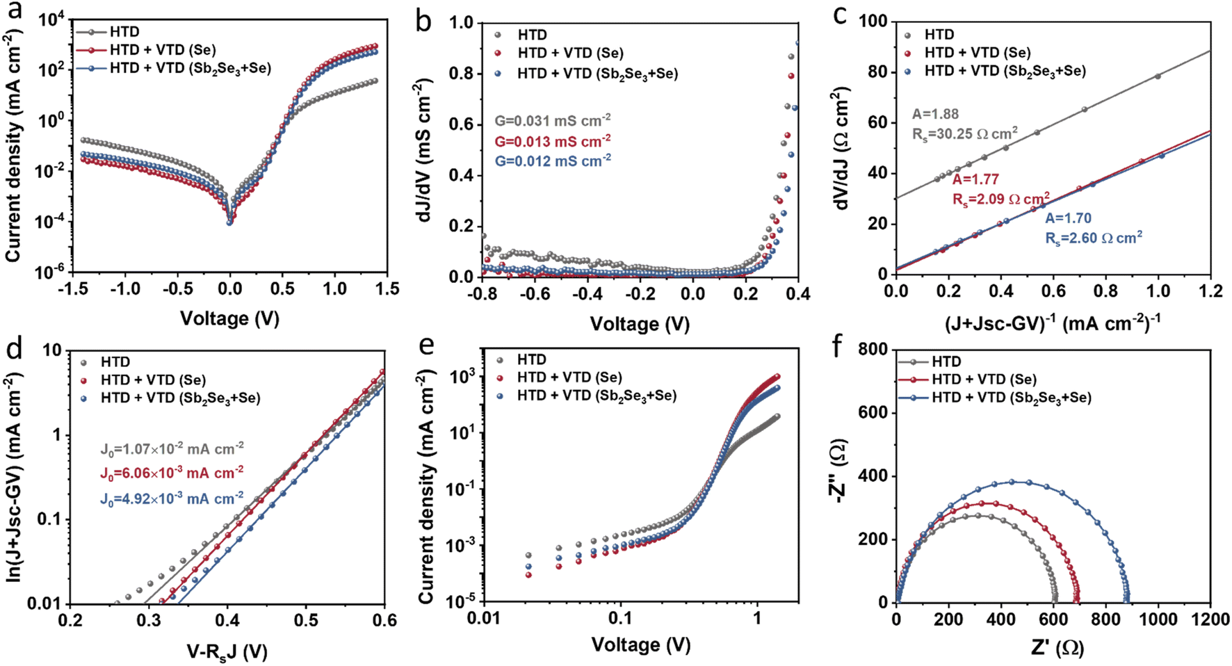 | ||
| Fig. 5 Charge transport behaviors of the representative Sb2(S,Se)3 devices: (a) semi-logarithmic dark J–V plots, (b) dJ dV−1versus V plots for G, (c) dV/dJ versus (J + Jsc−GV) plots for extracting Rs and A, (d) ln(J + Jsc − GV) versus V − RsJ plots for extracting J0, (e) SCLC spectra derived from the dark J–V curves, and (f) Nyquist plots extracted from IS. | ||
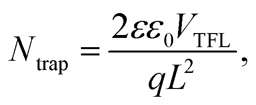
The defect states were further investigated under dark conditions using the standard space charge-limited current (SCLC) method.41Fig. 5a shows the logarithmic J–V characteristic curves of Sb2(S,Se)3 devices, which can be divided into three regions: the ohmic region (at low voltages), the trap-filled limit (TFL) region (at intermediate voltages), and the Child region (at high voltages). When the applied bias exceeds the kink point in the TFL region, the current experiences a sudden increase, indicating that the trap states have been fully filled by the injected carriers. The onset voltages of the TFL regions (VTFL) for the HTD, HTD + VTD (Se), and HTD + VTD (Sb2Se3 + Se) devices were determined to be 0.32, 0.27, and 0.26 V, respectively. The trap states density Ntrap can then be estimated by the following eqn (2):
 | (2) |
values (Table 2). As previously mentioned, the second-stage VTD process was conducted in a Se-rich atmosphere. It has been repeatedly reported that Sb2Se3 prepared under Se-poor conditions is susceptible to the formation of donor-like defects such as VSe and SbSe, which are known to degrade device performance.32,33,43,44 The Se-rich VTD process effectively passivates these defects enhancing the photovoltaic performance of HTD + VTD (Se) and HTD + VTD (Sb2Se3 + Se) devices.
Impedance spectroscopy (IS) allows for determining the recombination resistance and provides key information about the interface quality of a solar device. The resulting Nyquist plots are presented in Fig. 5f. The low-frequency arc of the impedance spectra represents the recombination resistance Rrec of the device. The solar devices with modified bandgap gradient (HTD + VTD (Se) and HTD + VTD (Sb2Se3 + Se)) display larger Rrec values of ∼690 and ∼880 Ω, respectively. The increase in Rrec points to improved carrier transport and suppressed carrier recombination, ultimately contributing to the enhanced FF in the corresponding solar cells.
Conclusions
The certified PCE of the Sb2(S,Se)3 solar cells has recently reached 10%, showcasing the potential of Sb2(S,Se)3 as a promising candidate for next-generation photovoltaic materials. However, as a newcomer in thin-film solar cells, further efforts are required to advance antimony chalcogenide photovoltaic technology. One crucial aspect in enhancing the efficiency of Sb2(S,Se)3 solar cells is the utilization of bandgap engineering, where an appropriate band gradient plays a vital role in promoting efficient carrier collection and reducing carrier recombination. In this work, we propose a hybrid growth method that combines the first-stage hydrothermal deposition process with the second-stage vapor transport deposition stage, allowing for the manipulation of the unfavorable band gradient. This approach facilitates hole transport and suppresses carrier recombination, resulting in significant improvements in key performance metrics, such as Jsc and FF, ultimately leading to enhanced overall cell efficiency. This research offers fresh perspectives on bandgap engineering for Sb2(S,Se)3 solar cells and establishes a solid foundation for the development of high-performance Sb2(S,Se)3-based photovoltaic devices.Author contributions
Y. W., S. J., and B. S. conceptualized the project. Y. W. and S. J. designed the experiments, analyzed the data, and wrote the original draft with input from all the authors, contributing equally to this work. C. M. and J. C. conducted the impedance spectroscopy measurements. H. J. performed the transmission electron microscopy measurements, provided the relevant analysis, and revised the manuscript. B. S. supervised the project.Conflicts of interest
There are no conflicts to declare.Acknowledgements
This research was supported in part by the National Research Foundation of Korea (NRF) grant funded by the Korea Government (MSIT) (no. NRF-2018R1A5A1025594 and NRF-2022M3H4A1A03074093) and in part by the program of Phased development of carbon neutral technologies through NRF funded by Ministry of Science and ICT (no. NRF-2022M3J1A1064212).References
- W. Yang, J. Ahn, Y. Oh, J. Tan, H. Lee, J. Park, H. C. Kwon, J. Kim, W. Jo and J. Kim, Adv. Energy Mater., 2018, 8, 1702888 CrossRef
.
- M. Ishaq, H. Deng, S. Yuan, H. Zhang, J. Khan, U. Farooq, H. Song and J. Tang, Sol. RRL, 2018, 2, 1800144 CrossRef
- J. Dong, Y. Liu, Z. Wang and Y. Zhang, Nano Sel., 2021, 2(10), 1818–1848 CrossRef CAS
- S. Agarwal, V. Nandal, H. Yadav and K. Kumar, J. Appl. Phys., 2021, 129, 203101 CrossRef CAS
- W. Yang, J. H. Kim, O. S. Hutter, L. J. Phillips, J. Tan, J. Park, H. Lee, J. D. Major, J. S. Lee and J. Moon, Nat. Commun., 2020, 11, 861 CrossRef CAS PubMed
- R. Tang, X. Wang, W. Lian, J. Huang, Q. Wei, M. Huang, Y. Yin, C. Jiang, S. Yang and G. Xing, Nat. Energy, 2020, 5, 587–595 CrossRef CAS
- X. Wang, R. Tang, C. Jiang, W. Lian, H. Ju, G. Jiang, Z. Li, C. Zhu and T. Chen, Adv. Energy Mater., 2020, 10, 2002341 CrossRef CAS
- Y. Zhao, S. Wang, C. Jiang, C. Li, P. Xiao, R. Tang, J. Gong, G. Chen, T. Chen and J. Li, Adv. Energy Mater., 2022, 12, 2103015 CrossRef CAS
- J.-H. Yang, W.-J. Yin, J.-S. Park, J. Ma and S.-H. Wei, Semicond. Sci. Technol., 2016, 31, 083002 CrossRef
- M. Nakamura, K. Yamaguchi, Y. Kimoto, Y. Yasaki, T. Kato and H. Sugimoto, IEEE J. Photovolt., 2019, 9, 1863–1867 Search PubMed
- T. Dullweber, U. Rau and H. Schock, Sol. Energy Mater. Sol. Cells, 2001, 67, 145–150 CrossRef CAS
- J. Ramanujam and U. P. Singh, Energy Environ. Sci., 2017, 10, 1306–1319 RSC
- Y. Wang, T. Muryobayashi, K. Nakada, Z. Li and A. Yamada, Sol. Energy Mater. Sol. Cells, 2019, 201, 110070 CrossRef CAS
- J. Gong, Y. Kong, J. Li, K. Wang, X. Wang, Z. Zhang, Z. Ding and X. Xiao, Nano Energy, 2019, 62, 205–211 CrossRef CAS
- S. Ji, T. Hayakawa, N. Suyama, K. Nakada and A. Yamada, Jpn. J. Appl. Phys., 2020, 59, 041003 CrossRef CAS
- T. Umehara, S. Iinuma and A. Yamada, Electron. Mater. Lett., 2016, 12, 479–483 CrossRef CAS
- K.-J. Yang, D.-H. Son, S.-J. Sung, J.-H. Sim, Y.-I. Kim, S.-N. Park, D.-H. Jeon, J. Kim, D.-K. Hwang and C.-W. Jeon, J. Mater. Chem. A, 2016, 4, 10151–10158 RSC
- M. Neuwirth, E. Seydel, J. Seeger, A. Welle, H. Kalt and M. Hetterich, Sol. Energy Mater. Sol. Cells, 2018, 182, 158–165 CrossRef CAS
- T. Zhou, J. Huang, S. Qian, X. Wang, G. Yang, B. Yao, Y. Li, Y. Jiang and Y. Liu, ACS Appl. Mater. Interfaces, 2022, 15(1), 1073–1084 CrossRef PubMed
- Z. Xu, Q. Gao, C. Cui, S. Yuan, D. Kou, Z. Zhou, W. Zhou, Y. Meng, Y. Qi and M. Ishaq, Adv. Funct. Mater., 2023, 33, 2209187 CrossRef CAS
- J. Kim and B. Shin, Electron. Mater. Lett., 2017, 13, 373–392 CrossRef CAS
- A. Lafuente-Sampietro, K. Yoshida, S. Wang, S. Ishizuka, H. Shibata, N. Sano, K. Akimoto and T. Sakurai, Sol. Energy Mater. Sol. Cells, 2021, 223, 110948 CrossRef CAS
- W. Liu, H. Li, B. Qiao, S. Zhao, Z. Xu and D. Song, Sol. Energy, 2022, 233, 337–344 CrossRef CAS
- M. Nicolás-Marín, J. Gonzalez-Castillo, O. Vigil-Galan and M. Courel, J. Phys. D: Appl. Phys., 2022, 55, 303001 CrossRef
- Y. Zhao, S. Wang, C. Li, B. Che, X. Chen, H. Chen, R. Tang, X. Wang, G. Chen and T. Wang, Energy Environ. Sci., 2022, 15, 5118–5128 RSC
- S. Wang, Y. Zhao, B. Che, C. Li, X. Chen, R. Tang, J. Gong, X. Wang, G. Chen and T. Chen, Adv. Mater., 2022, 34, 2206242 CrossRef CAS PubMed
- K. Li, Y. Lu, X. Ke, S. Li, S. Lu, C. Wang, S. Wang, C. Chen and J. Tang, Sol. RRL, 2020, 4, 2000220 CrossRef CAS
- C. Liu, S. Wu, Y. Gao, Y. Feng, X. Wang, Y. Xie, J. Zheng, H. Zhu, Z. Li and R. E. Schropp, Adv. Funct. Mater., 2022, 2209601 CrossRef CAS
- W. Han, D. Gao, R. Tang, Y. Ma, C. Jiang, G. Li, T. Chen and C. Zhu, Sol. RRL, 2021, 5, 2000750 CrossRef CAS
- X. Jin, Y. Fang, T. Salim, M. Feng, Z. Yuan, S. Hadke, T. C. Sum and L. H. Wong, Adv. Mater., 2021, 33, 2104346 CrossRef CAS PubMed
- Y. Huang, R. Tang, G. Wang, G. Li, B. Che, Y. Wang, W. Lian, C. Zhu and T. Chen, J. Mater. Chem. A, 2022, 10, 9892–9901 RSC
- J. Kim, S. Ji, Y. Jang, G. Jeong, J. Choi, D. Kim, S.-W. Nam and B. Shin, Sol. RRL, 2021, 5, 2100327 CrossRef CAS
- G. Jeong, S. Ji, J. Choi, J. Jung and B. Shin, Faraday Discuss., 2022, 239, 263–272 RSC
- M. Nakamura, K. Tada, T. Kinoshita, T. Bessho, C. Nishiyama, I. Takenaka, Y. Kimoto, Y. Higashino, H. Sugimoto and H. Segawa, Iscience, 2020, 23, 101817 CrossRef CAS PubMed
- R. Carron, C. Andres, E. Avancini, T. Feurer, S. Nishiwaki, S. Pisoni, F. Fu, M. Lingg, Y. E. Romanyuk and S. Buecheler, Thin Solid Films, 2019, 669, 482–486 CrossRef CAS
-
D. B. Williams, C. B. Carter, D. B. Williams and C. B. Carter, Transmission Electron Microscopy: A Textbook for Materials Science, 2009, pp. 53–71 Search PubMed
- N. Tideswell, F. Kruse and J. McCullough, Acta Crystallogr., 1957, 10, 99–102 CrossRef CAS
- G. Li, J. Dong, P. Xiao, B. Che, Y. Huang, Y. Zhang, R. Tang, C. Zhu and T. Chen, Sci. China Mater., 2022, 1–7 Search PubMed
- Y. Cao, C. Liu, J. Jiang, X. Zhu, J. Zhou, J. Ni, J. Zhang, J. Pang, M. H. Rummeli and W. Zhou, Sol. RRL, 2021, 5, 2000800 CrossRef CAS
- S. S. Hegedus and W. N. Shafarman, Prog. Photovolt.: Res. Appl., 2004, 12, 155–176 CrossRef CAS
- R. H. Bube, J. Appl. Phys., 1962, 33, 1733–1737 CrossRef CAS
- E. A. Duijnstee, J. M. Ball, V. M. Le Corre, L. J. A. Koster, H. J. Snaith and J. Lim, ACS Energy Lett., 2020, 5, 376–384 CrossRef CAS
- X. Liu, X. Xiao, Y. Yang, D. J. Xue, D. B. Li, C. Chen, S. Lu, L. Gao, Y. He and M. C. Beard, Prog. Photovolt.: Res. Appl., 2017, 25, 861–870 CrossRef CAS
- M. Huang, P. Xu, D. Han, J. Tang and S. Chen, ACS Appl. Mater. Interfaces, 2019, 11, 15564–15572 CrossRef CAS PubMed
Footnotes |
| † Electronic supplementary information (ESI) available. See DOI: https://doi.org/10.1039/d3ta05489f |
| ‡ These authors contributed equally to this work. |
| This journal is © The Royal Society of Chemistry 2023 |