
First-principles study of intrinsic and hydrogen point defects in the earth-abundant photovoltaic absorber Zn3P2†
Zhenkun
Yuan
 ,
Yihuang
Xiong
and
Geoffroy
Hautier
*
,
Yihuang
Xiong
and
Geoffroy
Hautier
*
Thayer School of Engineering, Dartmouth College, Hanover, New Hampshire 03755, USA. E-mail: geoffroy.hautier@dartmouth.edu
First published on 10th September 2023
Abstract
Zinc phosphide (Zn3P2) has had a long history of scientific interest largely because of its potential for earth-abundant photovoltaics. To realize high-efficiency Zn3P2 solar cells, it is critical to understand and control point defects in this material. Using hybrid functional calculations, we assess the energetics and electronic behavior of intrinsic point defects and hydrogen impurities in Zn3P2. All intrinsic defects are found to act as compensating centers in p-type Zn3P2 and have deep levels in the band gap, except for zinc vacancies which are shallow acceptors and can act as a source of doping. Our work highlights that zinc vacancies rather than phosphorus interstitials are likely to be the main source of p-type doping in as-grown Zn3P2. We also show that Zn-poor and P-rich growth conditions, which are usually used for enhancing p-type conductivity of Zn3P2, will facilitate the formation of certain deep-level defects (PZn and Pi) which might be detrimental to solar cell efficiency. For hydrogen impurities, which are frequently present in the growth environment of Zn3P2, we study interstitial hydrogen and hydrogen complexes with vacancies. The results suggest small but beneficial effects of hydrogen on the electrical properties of Zn3P2.
1. Introduction
The II–V semiconductor zinc phosphide (Zn3P2) is a promising light-absorbing material for cost-effective thin-film photovoltaics.1,2 It consists of earth-abundant elements and shows attractive optoelectronic properties as a solar absorber: a direct band gap of ∼1.5 eV, a high absorption coefficient of over 104 cm−1,3,4 and minority-carrier diffusion lengths (in the bulk crystal) of up to a few micrometers.5,6 Zn3P2-based solar cells received considerable attention from the late 1970s to the 1990s. However, the efficiencies have been achieved as yet are far below the Shockley–Queisser limit (∼33%).7–12 The highest efficiency of Zn3P2 solar cells was reported in 1981 and has remained since then at just 5.96%.8More recently, Zn3P2 solar cells have seen a resurgence of interest. Notably, researchers have developed fabrication methods for highly crystalline, reproducible Zn3P2 thin films on commercially available substrates which had long been a challenge.13–15 The attainment of high-quality samples paves the way for addressing another persistent challenge: control of point defects and doping in bulk Zn3P2.16,17
As-grown Zn3P2 crystals and thin films nearly always exhibit p-type conductivity, the origin of which is believed due to intrinsic point defects.18 Because conductivity has been observed to vary with the phosphorus partial pressure in the growth or annealing environment, it has been commonly attributed to phosphorus interstitials (Pi).12,18–21 Despite no direct experimental observations of phosphorus interstitials or their involvement in p-type doping, this assignment has been supported by an early first-principles investigation based on semilocal density-functional theory (DFT), which has suggested that phosphorus interstitials are the most prevalent acceptor species in Zn3P2.22 However, a subsequent first-principles study, using more accurate hybrid functional, has shown that Pi is a deep acceptor and has much higher formation energy than another acceptor, the zinc vacancy (VZn).23 In order to clarify these conflicting results, recently Stutz et al. and Paul et al. studied the effect of compositional stoichiometry variations on the structural, electrical, and optical properties of monocrystalline Zn3P2 thin films, yet a conclusive identification of the source for the p-type conductivity, whether it is due to Pi or VZn, has remained elusive.24,25 On the other hand, less attention has been devoted to identifying deep-level defects in Zn3P2, in spite of accumulating experimental evidence for presence of deep levels in the band gap of Zn3P2.26–28 Deep-level defects may act as nonradiative carrier recombination centers which would limit the efficiency of Zn3P2 solar cells.
In addition to intrinsic defects, there is strong experimental evidence that hydrogen impurities are likely present in Zn3P2 samples: growth of Zn3P2 thin films is conventionally carried out in H2 atmosphere and/or PH3 gas using techniques such as physical vapor transport,4,29 chemical vapor deposition30,31 and metal–organic chemical vapor deposition,32–35 ionized cluster beam deposition,36 and RF sputtering.37,38 Sometimes the samples were also annealed in H2 gas following growth.33,37,39–41 It is known that unintentional hydrogen doping in oxides and III–V nitrides has a strong impact on the electrical properties of these materials.42–44 Therefore, in order to avoid uncontrolled influence of hydrogen impurities, it is important to understand the behavior of hydrogen in Zn3P2.
Using first-principles calculations with a hybrid functional, we study intrinsic point defects and hydrogen impurities in Zn3P2: zinc and phosphorus vacancies (VZn and VP), interstitials (Zni and Pi), and antisites (ZnP and PZn); for hydrogen impurities, hydrogen interstitial (Hi) and hydrogen-vacancy complexes are investigated. The present work assesses the energetics and electronic behavior of the defects based on their calculated formation energies and charge transition levels. Comparing our results with experiments and previous calculations, we address the open questions about the shallow or deep nature of the defects in Zn3P2. Our work clarifies the likely defects leading to p-type doping in Zn3P2 and the possible deep-level defects which may act as nonradiative recombination centers. It also elucidates the role of hydrogen in doping of Zn3P2.
2. Intrinsic point defects
We have performed hybrid functional calculations for the intrinsic defects VZn, VP, Zni, Pi, ZnP, and PZn in Zn3P2. Fig. 1 shows the calculated formation energies for these defects, under Zn-poor (P-rich) and Zn-rich (P-poor) chemical-potential conditions. Details about the calculation methods and the chemical potentials of Zn and P can be found in the Methods section. We find, in Fig. S1 of the ESI,† a rather small chemical-potential region for which Zn3P2 is thermodynamically stable, due to strong phase competition from ZnP2 (another stable crystalline phase in the Zn–P system).45 Note that the terms “rich” and “poor” used in Fig. 1 and S1† do not represent the actual compositional stoichiometry of experimental samples but rather they correspond to the endpoints of the chemical-potential region that stabilizes compositionally stoichiometric Zn3P2, so the results presented in Fig. 1 are for the intrinsic defects in (nearly) stoichiometric samples.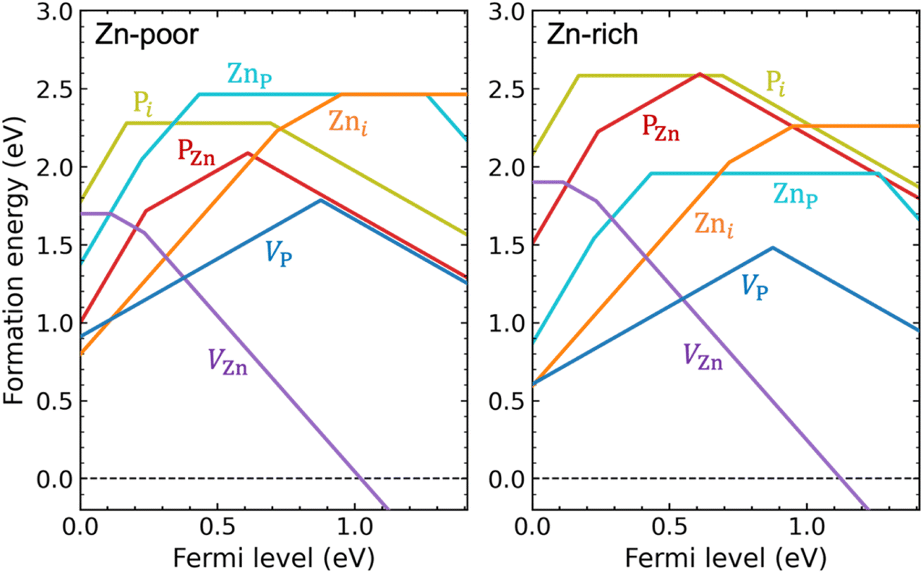 | ||
| Fig. 1 Formation energies as a function of Fermi level for intrinsic point defects in Zn3P2, under Zn-poor/P-rich (left) and Zn-rich/P-poor (right) conditions. The zero of the Fermi level is set at the VBM and the upper bound corresponds to the conduction-band minimum (CBM). For the same Fermi-level value, only formation energy for the most stable charge state is shown, i.e., VZn: 0, −, 2−; VP: +, −; Zni: 2+, +, 0; Pi: 3+, 0, −; ZnP: 3+, 2+, 0, 2−; PZn: 3+, +, −. Kinks in each curve indicate transitions between different charge states (values of the thermodynamic transition levels are also listed in Table S1 of the ESI†). | ||
As shown in Fig. 1, the VZn and Zni behave exclusively as an acceptor and as a donor, respectively. In contrast, all other intrinsic defects, including VP, Pi, ZnP, and PZn, are amphoteric: they exist in donor states when the Fermi level is low in the band gap while in acceptor states when the Fermi level is high in the band gap. The amphoteric behavior of these defects is related to the unique ability for phosphorus to occur in multiple oxidation states from P3− to P5+.
We find that the VZn behaves as a shallow acceptor and is the only intrinsic defect that can act as a source of p-type doping in Zn3P2. The VZn gives rise to two acceptor levels in the band gap: a shallow (0/−) transition level at 0.11 eV and a relatively deep (−/2−) transition level at 0.23 eV above the valence band (see Fig. 1). For reference, the calculated single-particle defect states of VZn can be found in Fig. S2 of the ESI.† The formation energy of VZn is relatively high for Fermi-level positions close to the valence-band maximum (VBM), even under Zn-poor/P-rich condition.
Contrary to the commonly accepted assumption that phosphorus interstitials are the cause of p-type conductivity in as-grown Zn3P2,12,18–21 we find that phosphorus interstitials cannot possibly contribute to p-type doping. First and foremost, Pi gives rise to a very deep acceptor level ε(0/−) = 0.69 eV (see Fig. 1); thus, it can hardly provide holes to the valence band through thermal excitation. Second, for most Fermi-level positions in the lower part of the band gap, Pi will exist in the neutral charge state (being electrically inactive). Even when the Fermi level is close to the valence band, Pi can also be stable in the +3 charge state, with a (3+/0) transition level at 0.17 eV above the VBM. The existence of this positive charge state, which removes three holes from the valence band, suggests that phosphorus interstitials could act as compensating centers in p-type Zn3P2 (though this happens for Fermi level below 0.17 eV). Third, Pi has a high formation energy and is therefore not expected to form in significant concentrations in (nearly) stoichiometric Zn3P2 samples.
Fig. 2a shows that in the neutral charge state, the Pi adopts a split-interstitial configuration in which the interstitial P shares a lattice site with one of the lattice P atoms, consistent with previous calculations.22,23 Similar split-interstitial configuration has been found for the nitrogen interstitial in GaN.46 The plotted spin density shows that the neutral Pi is characterized by a highly localized hole state, with most of the charge located on the interstitial P atom and the bonded lattice P atom. The calculated single-particle energy level of the hole state is located well above the VBM (more specifically, right below the CBM), as indicated by the blue line in Fig. 2b. When the Pi becomes negatively charged, there is a large relaxation of the interstitial and the surrounding atoms, yet the split-interstitial configuration is largely kept, as shown in Fig. 2c. As a result, the single-particle defect level is pushed down to below the VBM, as indicated by the red line in Fig. 2b. Interestingly, as indicated by the black dashed line in Fig. 2b, the average of the two single-particle defect levels is 0.62 eV above the VBM, which happens to provide a good estimate of the (0/−) transition level (0.69 eV).
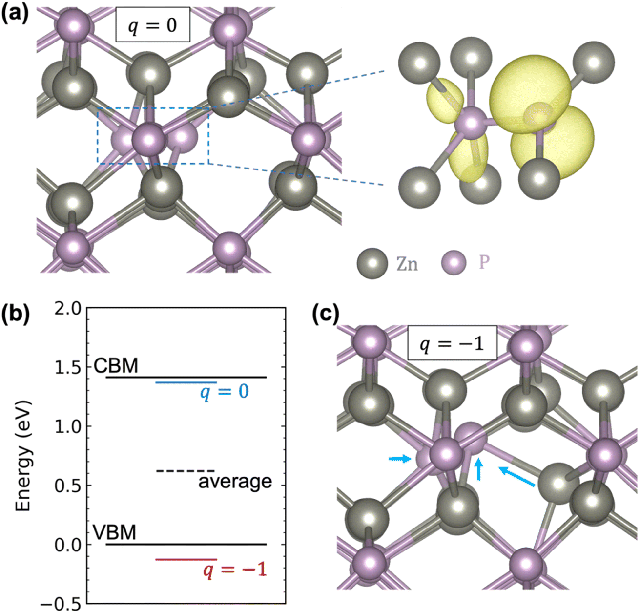 | ||
| Fig. 2 (a) Local atomic geometry and spin density (isosurface at 10% of the maximum in yellow) associated with the localized hole state of the Pi in the neutral charge state (q = 0). The Pi adopts a split-interstitial configuration in which the interstitial P shares a lattice site with a lattice P atom. (b) Single-particle energy levels of the localized hole state of the Pi, before and after being occupied (with both atomic and electronic relaxations). The energy of the VBM is set to zero. To plot the single-particle defect levels and the bulk band edges (the VBM and CBM) together, a simple alignment using the deep core level of the farthest atom from the defect site is considered. (c) Local atomic geometry of the Pi in the q = −1 charge state, with the arrows indicating the local atomic relaxations. | ||
All other intrinsic defects, including VP, Zni, ZnP, and PZn, have deep transition levels in the band gap, as seen in Fig. 1. The Zni is a double donor with two deep levels: a (+/0) transition level at 0.95 eV and a (2+/+) transition level at 0.72 eV above the VBM. For VP, the formation energies of VP+ and VP− intersect at 0.88 eV above the VBM, and V0P is energetically unstable compared to either VP+ or VP− over the entire range of Fermi-level positions in the band gap; this is characteristic of a negative-U behavior. Similar to VP, the PZn forms a deep transition level between +1 and −1 charge states at 0.61 eV above the VBM. The ZnP has a deep (2+/0) transition level (also a negative-U transition) at 0.43 eV above the VBM. Besides these deep levels, the PZn (3+/+) transition level is close to the VBM, and the ZnP (3+/2+) and (0/2−) transition levels are close to the VBM and CBM, respectively.
Similar to the Pi, the VP, ZnP, and PZn will contribute to compensation in p-type Zn3P2, due to their amphoteric behavior. As indicated in Fig. 1, the VP and Zni are the main compensating intrinsic defects in p-type Zn3P2. In addition, depending on growth conditions and on the p-type doping level (i.e., the Fermi-level position), the formation energy of ZnP and PZn can be as low as ∼1 eV, suggesting that both defects can form in significant concentrations and thus also be important compensating centers. From Fig. 1 we can see that compensation of p-type doping is reduced under Zn-poor/P-rich condition where the VP and Zni have higher formation energy (though the formation energy of PZn is lowered under this condition).
3. Comparison with experiments and discussion
The type of possible doping or dopability of a material are largely controlled by compensation. Hole-killer (electron-killer) defects can prevent p-type (n-type) doping.47,48 Our first-principles results indicate that Zn3P2 clearly favors p-type doping, because no hole-killer defects will pin the Fermi level while the electron-killer VZn will pin the Fermi level and prevent n-type doping even in the presence of shallow extrinsic donors. The p-type doping of Zn3P2 is favored under Zn-poor/P-rich conditions, where both the formation energy of VZn acceptors and the compensation will be reduced. Our finding agrees with the experimentally observed p-type nature of Zn3P2.12,18–21Our results suggest that VZn (but not Pi) is a source of p-type conductivity in as-grown Zn3P2. This disagrees with the previous reports that p-type conductivity in Zn3P2 is due to Pi which has been based on experimental observations that conductivity of Zn3P2 samples varies with the phosphorus partial pressure in the growth or annealing environment.12,18–21 Here we take a closer look at ref. 18 and 19. In ref. 18, Zn3P2 samples were post-growth annealed over a range of equilibrium vapor compositions, and conductivity was observed to be increased when changing from Zn-rich annealing conditions (zinc vapor) to P-rich annealing conditions (phosphorus vapor). In ref. 19, electrical measurements were performed on a set of samples with the P/(Zn + P) ratio varying from 0.39 (which corresponds to a P-poor sample) to 0.4 (which corresponds to a stoichiometric sample), showing increased conductivity. For both studies, the observed conductivity increase can be explained by an enhancement of the VZn concentration and a reduction of the VP and Zni concentrations. It should be noted that since Zn3P2 is a binary compound, a P-rich (P-poor) condition means a Zn-poor (Zn-rich) condition. We conclude that our results are in line with the experimental observations.
The more recent experimental work by Stutz et al.,24 is also of interest. This work studied monocrystalline, nonstoichiometric P-rich Zn3P2 thin films and found increasing lattice expansion when the compositional stoichiometry varies from Zn2.98P2.02 (Zn/P = 1.47) to Zn2.75P2.25 (Zn/P = 1.22) to Zn2.67P2.33 (Zn/P = 1.15). Stutz et al. interpreted their results in terms of the formation of Pi, and also suggested that many of the defects in their samples are in neutral charge state (based on the fact that in all three samples, the compositionally induced defect density is about five orders of magnitude higher than carrier density). Our results support the analysis of Stutz et al., whereas further indicate that it is necessary to account for the PZn in understanding the defects in non-stoichiometric P-rich Zn3P2 samples; that is, an excess of P leads to PZn and Pi and facilitates the formation of VZn. In this case, the VZn acceptors are expected to be heavily compensated by PZn, and most Pi defects will be in the neutral charge state as discussed above. Within this picture, non-stoichiometric P-rich Zn3P2 samples should be highly compensated.
Fig. 3 shows a comparison of our calculated positions of charge transition levels with experimental values obtained by deep-level transient spectroscopy (DLTS; on Zn3P2 polycrystals),27,28 electrical transport measurements (on Zn3P2 single crystals),26 and photoluminescence spectroscopy (on monocrystalline, nonstoichiometric P-rich Zn3P2 thin films).24 Note that the experimental results have been classified as acceptor levels or hole-trap levels in the original work. In Fig. 3 we also plot the relevant transition levels involving thermodynamically unstable charge states: the (+/0) and (0/−) transition levels of both VP and PZn, and the (2+/+) and (+/0) transition levels of ZnP (for more information on the charge-state transitions we refer to Fig. S3 of the ESI†); such levels may be detected by transient spectroscopies like DLTS, but a more likely explanation is the presence of complex defects. In the following, we attempt to identify the origin of the experimentally observed defect levels. This assignment is tentative and based purely on the defect energy levels. It does not take into account defect clusters, extended defects, or extrinsic impurities which could be present in the experimental samples.49
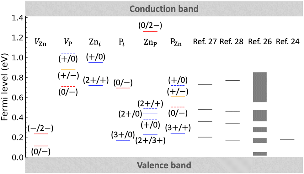 | ||
| Fig. 3 Comparison of our calculated thermodynamic transition levels (between different charge states q and q′) with experimental values reported in the literature. The red, blue, and orange solid lines indicate the calculated acceptor, donor, and (+/−) transition levels, respectively. The dashed lines indicate the relevant transition levels involving thermodynamically unstable charge states. Experimental data are taken from ref. 24 and 26–28; they have been reported as acceptor levels or hole-trap levels in the original work. | ||
First, we assign the acceptor level lying at ∼0.14–0.2 eV, commonly observed in the experiments, to the (−/2−) transition level of VZn. In ref. 26 and another electrical transport experiment,50 it has been found that in Zn3P2 samples with high hole density (∼1017 cm−3), there is only one important acceptor level lying at ∼0.05 eV. This shallow acceptor level is assigned tentatively to the (0/−) transition level of VZn. Second, for the experimentally observed hole-trap levels, our speculations are as follows. The level lying at 0.25–0.30 eV (observed by electrical transport measurements) is assigned tentatively to the PZn (3+/+) transition level. The level lying at ∼0.35 eV (detected by DLTS) is identified tentatively as the ZnP (+/0) transition level. The level lying at ∼0.46 eV (DLTS) may be assigned to ZnP (2+/0) or (2+/+) or PZn (0/−) transition levels. The level lying at ∼0.75 eV (DLTS) may be related to the VP (0/−), Zni (2+/+), Pi (0/−), or PZn (+/0) transitions.
Deep levels in a solar absorber could cause nonradiative recombination of photo-generated carriers and hence be detrimental to the device performance.51–54 Our identification of the intrinsic defects having deep levels in Zn3P2 will help optimize the absorber by control of these defects. However, suppressing the formation of the deep-level defects is likely to be challenging for Zn3P2. For instance, while Zn-poor/P-rich conditions are needed to enhance p-type doping, such conditions will facilitate the formation of PZn and Pi which possess deep levels. This implies that good photovoltaic performance is not guaranteed for nonstoichiometric P-rich Zn3P2 samples which have become the focus of recent experimental studies.17,24,25 This analysis would however require a systematic study of the nonradiative carrier capture coefficients (cross sections) which could vary considerably between different deep levels,55–59 which is beyond the scope of the present work.
4. Comparison with previous calculations
The first DFT study of intrinsic defects in Zn3P2 by Demers et al. used a semilocal functional.22 One of the main conclusions of ref. 22 is that phosphorus interstitials are the most prevalent acceptors. Because of the inherent limitations of semilocal functionals in predicting band gaps for semiconductors,60–62 Demers et al. corrected the band gap of Zn3P2 using an extrapolation method that is often difficult to justify.60 In light of this deficiency, we believe that the calculated defect energetics in ref. 22 suffer from considerable uncertainties.On the other hand, Yin et al. have reported hybrid-functional calculations for intrinsic defects in Zn3P2.23 Both our results and those of Yin et al. agree that: (i) the VZn behaves as a shallow acceptor; (ii) the Pi gives rise to a deep acceptor level, and is energetically less favorable than VZn. However, some notable differences exist. As listed in Table S2 of the ESI,† the charge transition levels reported by Yin et al. are systematically shallower than ours. For instance, the (0/−) transition level of Pi is 0.30 eV in ref. 23 while it is 0.69 eV in the present work. In addition, Yin et al. have shown that VP and Pi behave exclusively as a donor and as an acceptor, respectively, while we find amphoteric behavior of both defects. We attribute these discrepancies to the apparent lack of spin polarization and proper supercell-size corrections in the defect calculations in ref. 23.
5. Effects of hydrogen on doping and defect passivation
We now turn to hydrogen impurities in Zn3P2. We have considered hydrogen interstitial (Hi) and hydrogen in zinc and phosphorus vacancies, and performed a careful search for their lowest-energy configurations. It is seen in Fig. S4 of the ESI† that H0i and Hi− are most stable at the tetrahedral site and Hi+ is most stable at the bond-center site. For a single H in the zinc vacancy, we initially incorporated it on the substitutional Zn site but found that it moves off to bind with one of the four surrounding P atoms; it is thus regarded as a H + VZn complex rather than a substitutional HZn. The VZn can trap a second H to form a 2H + VZn complex in which each H binds with one P atom. For a single H in the phosphorus vacancy, the H is also located off-center but binds with two Zn atoms, resulting in a H + VP complex.Fig. 4 plots the calculated formation energies for the H-related point defects, under Zn-poor/P-rich condition (as in Fig. 1) and at two different chemical potentials of H (μH): (i) μH = 0, i.e., the H-rich limit; (ii) a lower μH of −0.45 eV (this value is a more realistic choice of μH; it can be obtained through equilibrium with H2 gas at 400 °C and partial pressure of 0.01 atm in the ideal-gas model;63,64 see the Methods section). Let us first analyze the electronic behavior of the H-related defects. As can be seen, Hi is amphoteric with a (+/−) transition level in the band gap, as commonly found for hydrogen interstitial in semiconductors.65 Since the (+/−) transition level is 0.57 eV above the VBM, Hi acts as a compensating center in p-type Zn3P2. Further, hydrogen passivates the dangling bonds of the vacancies and hence reduce their charge states. The H + VZn complex is a single acceptor with a (0/−) transition level 0.09 eV above the VBM, which is slightly shallower than that of isolated VZn (0.11 eV). The 2H + VZn complex has no gap states and does not introduce any defect level in the band gap. The H + VP complex is a single donor with a (+/0) transition level just 0.13 eV above the VBM.
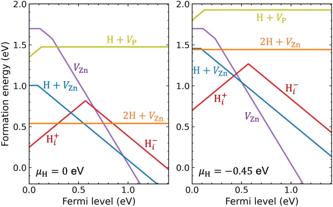 | ||
| Fig. 4 Formation energies as a function of Fermi level for hydrogen interstitial (Hi) and hydrogen-vacancy complexes, including the H + VZn, 2H + VZn, and H + VP, in Zn3P2, under Zn-poor/P-rich condition and at two different chemical potentials of H (μH): the H-rich limit μH = 0 eV (left panel) and a lower μH at −0.45 eV (right panel). For comparison the formation energy of VZn is also depicted. | ||
Under the H-rich limit (left panel of Fig. 4), we see that the Hi+, H + VZn, and 2H + VZn have low formation energy. In contrast, the H + VP has relatively high formation energy. Here and in the following, our implicit assumption is that we are considering p-type Zn3P2. Moving to the lower μH (right panel of Fig. 4), the formation energies of the H-related defects are increased, especially for the 2H + VZn complex. In addition, the formation energy of H + VZn and 2H + VZn becomes comparable to that of isolated VZn. Irrespective of μH, the binding energy of [H + VZn]− (2H + VZn), defined as the difference between the formation energy of [H + VZn]− (2H + VZn) and the sum of the formation energies of isolated VZn2− and Hi+, is found to be 1.2 eV (2.0 eV). This is quite a large value, indicating that hydrogen interacts strongly with zinc vacancies resulting in stable complexes. The binding energy of the H + VP with respect to isolated VP− and Hi+ is also found to be large (1.43 eV). This suggests that the H + VP complex would be stable if formed, despite having a relatively high formation energy. We also take note of the fact that interstitial hydrogen is expected to be quite mobile in crystalline semiconductors.66–68
It is thus found that when incorporated into Zn3P2, hydrogen is likely to form Hi+ and stable complexes with the VZn acceptors. Because, compared with isolated VZn, the H + VZn has shallower acceptor level and lower formation energies (under H-rich conditions), hydrogen incorporation may enhance p-type doping of Zn3P2. As shown in Fig. S5 of the ESI,† the calculated bulk hole density increases as μH approaches zero (the H-rich limit). Nevertheless, the enhancement of p-type doping by H + VZn is found to be small, because of the compensation by Hi+ and the competition from 2H + VZn (which is electrically inactive).
We are aware of the experimental work of Wang et al.39 and Bube,40 which show increased bulk hole density (by about an order of magnitude) in Zn3P2 samples as a result of high-temperature annealing in H2 gas. Yet, Bube40 noted a depletion of holes in the surface region of the samples after the annealing. Suda et al.37 reported that annealing Zn3P2 films in H2 gas reduces the resistivity by an order of magnitude. In another study, Suda et al.27 found that hydrogen plasma treatment of Zn3P2 removes a native hole-trap level at 0.2 eV above the VBM, which can be explained by passivation of VZn. Suda et al. also observed hydrogen passivation of deep hole-trap levels, and found that excessive hydrogenation creates a new hole-trap level at 0.13 eV above the VBM, which may be explained by formation of the H + VP complex. For hydrogen incorporation during the deposition of Zn3P2 films, Kakishita et al.36 found only a passivation effect of hydrogen, but not change in conductivity.
6. Conclusions
In conclusion, we have studied intrinsic point defects and hydrogen impurities in Zn3P2 using first-principles hybrid functional calculations. Among the intrinsic defects, only zinc vacancies are shallow acceptors and can act as a source of p-type doping. All other intrinsic defects, including the VP, Zni, Pi, ZnP, and PZn, will contribute to compensation in p-type Zn3P2. All of these defects are amphoteric (except for the Zni which is exclusively a donor), and they all have deep levels in the band gap. Control of the intrinsic defects by adjusting the growth conditions to enhance p-type doping may be challenging for Zn3P2 if the concentration of the deep-level defects has to be kept low. For instance, while Zn-poor/P-rich growth or annealing conditions are needed to enhance the concentration of VZn acceptors, such conditions will facilitate the formation of the deep PZn and Pi defects. Hydrogen impurities in Zn3P2 are likely to form Hi+ and stable complexes with the VZn acceptors. The H + VZn complex is a shallow acceptor which can contribute to doping, while the Hi+ will lead to compensation of holes and the 2H + VZn complex is electrically inactive. Due to the counteracting behavior of the H-related defects, the impact of hydrogen on p-type doping of Zn3P2 is predicted to be small.7. Methods
All the DFT calculations were performed using the projector augmented wave (PAW) pseudopotential method and hybrid functional of Heyd–Scuseria–Ernzerhof (HSE) as implemented in the VASP code.69–71 The wave functions were expanded in a plane-wave basis set with an energy cutoff of 400 eV. The tetragonal unit cell of Zn3P2 contains 40 atoms, and the Brillouin zone was sampled with a 4 × 4 × 3 Monkhorst–Pack k-point mesh. The HSE mixing parameter (α) was set to 0.32, which yields a band gap Eg = 1.41 eV and lattice parameters a = 8.076 Å and c = 11.388 Å for the unit cell, in agreement with the experimental values (Eg ∼1.5 eV, and lattice parameters a = 8.09 Å and c = 11.45 Å).4,72 This α value (0.32) was adopted in previous HSE hybrid-functional calculations in ref. 23; for consistency and comparison with ref. 23, we chose to use the same α value, instead of using a very slightly higher α to obtain a “perfect” match to the experimental band gap. A 2 × 2 × 2 supercell (which contains 320 atoms when it is defect free) was used for point-defect simulations, with a Γ-only k-point for the Brillouin-zone sampling. All atomic coordinates in supercells containing a point defect were fully relaxed until the residual atomic forces become less than 0.01 eV Å−1. Spin polarization was explicitly considered in all the defect calculations. Defect formation energies and thermodynamic charge transition levels were calculated using the standard first-principles formalism as detailed in ref. 61 and the PyCDT code.73 For charged defects, electrostatic correction and potential alignment were applied using the experimental static dielectric constant (ε0 = 11).74–76 Test calculations using an energy cutoff of 500 eV or a larger 3 × 3 × 2 supercell (720 atoms) show that the effect of energy cutoff is marginal and that the supercell size has an effect which should be less than about 0.05 eV (see Table S2†).Since the formation energy of a defect depends on the chemical potential of the elements involved in creating the defect, we have determined the chemical potential of Zn (μZn) and the chemical potential of P (μP) according to the following four relations:
| μZn < 0, |
| μP < 0, |
| μZn + 2μP < ΔHf (ZnP2), |
| 3μZn + 2μP = ΔHf (Zn3P2), |
The formation energy of the H-related point defects in Zn3P2 also depends on the chemical potential of H (μH). In the H-rich limit, μH = 0 eV [referenced to half the energy E(H2) of an H2 molecule at T = 0 K]. We have also considered the familiar situation of annealing in H2 gas at temperature T and partial pressure p, where μH is determined through equilibrium with H2 gas. In this case, μH is a well-established function of T and p:
The μHH2 gas(T, p) for moderate T and p can be obtained by an analytical expression arising from the ideal-gas model [see e.g., eqn (21) of ref. 63]. In the main text, we considered T = 400 °C and p = 0.01 atm, which gives μH = −0.45 eV.
Some defects like the phosphorus interstitial (Pi) and hydrogen-related defects involve large atomic relaxations. Their ground-state structures deviate considerably from the undistorted initial trial configurations. For these defects, care has been exercised in order to correctly determine their ground-state configurations. This includes, but not limited to, using a fairly large number of initial trial configurations (for different charge states). In the future, one can use the recently developed ShakeNBreak global potential-energy surface search method to help identify the ground-state defect structure.77,78
Finally, in order to check whether our choice of α = 0.32 for the HSE mixing parameter describes correctly the localized hole state of Pi0, the fulfillment of the generalized Koopmans' theorem has been examined.79–81 We find the non-Koopmans energy for Pi0, defined as ENK = ε(N) − [E(N + 1) − E(N)], to be small (0.12 eV). Here, ε(N) is the single-particle energy level of the localized hole state of P0i, and E(N + 1) − E(N) is the total-energy difference between Pi− (with atomic positions fixed to those of P0i) and P0i. The electrostatic finite-size correction was only applied to the total energy of Pi−, and ENK may still contain a small finite-size error. We conclude that the self-interaction error is relatively small in the HSE description of the localized hole state of P0i. We have also used the standard HSE06 functional (α = 0.25) to calculate the (0/−) transition level of the Pi, starting from the HSE06-calculated lattice parameters. The HSE06 band gap is 1.15 eV, not as close to experiment as the HSE (α = 0.32) band gap (1.41 eV). The HSE06 calculations also find a split-interstitial configuration of P0i, and yield a (0/−) transition level 0.54 eV above the VBM, compared to the value of 0.69 eV from the HSE calculation with α = 0.32.
Conflicts of interest
There are no conflicts of interest to declare.Acknowledgements
This work was supported by the U.S. Department of Energy, Office of Science, Basic Energy Sciences under award number DE-SC0023509. This research used resources of the National Energy Research Scientific Computing Center (NERSC), a DOE Office of Science User Facility supported by the Office of Science of the U.S. Department of Energy under contract no. DE-AC02-05CH11231 using NERSC award BES-ERCAP0023830.References
- C. Wadia, A. P. Alivisatos and D. M. Kammen, Environ. Sci. Technol., 2009, 43, 2072–2077 CrossRef CAS PubMed.
- Y. S. Lee, M. Bertoni, M. K. Chan, G. Ceder and T. Buonassisi, in 2009 34th IEEE Photovoltaic Specialists Conference (PVSC), DOI: DOI:10.1109/PVSC.2009.5411314.
- E. A. Fagen, J. Appl. Phys., 1979, 50, 6505–6515 CrossRef CAS.
- T. Suda, T. Nishimoto and S. Kurita, J. Cryst. Growth, 1988, 86, 430–435 CrossRef CAS.
- N. C. Wyeth and A. Catalano, J. Appl. Phys., 1979, 50, 1403–1407 CrossRef CAS.
- G. M. Kimball, A. M. Müller, N. S. Lewis and H. A. Atwater, Appl. Phys. Lett., 2009, 95, 112103 CrossRef.
- W. Shockley and H. J. Queisser, J. Appl. Phys., 1961, 32, 510–519 CrossRef CAS.
- M. Bhushan and A. Catalano, Appl. Phys. Lett., 1981, 38, 39–41 CrossRef CAS.
- P. S. Nayar and A. Catalano, Appl. Phys. Lett., 1981, 39, 105–107 CrossRef CAS.
- T. Suda, M. Kobayashi, A. Kuroyanagi and S. Kurita, Jpn. J. Appl. Phys., 1982, 21, 63 CrossRef CAS.
- M. Bhushan, Appl. Phys. Lett., 1982, 40, 51–53 CrossRef CAS.
- G. M. Kimball, N. S. Lewis and H. A. Atwater, in 35th IEEE Photovoltaic Specialists Conference (PVSC), DOI: DOI:10.1109/PVSC.2010.5614641.
- M. Zamani, E. Stutz, S. Escobar, R. R. Zamani, R. Paul, J.-B. Leran, M. Dimitrievska and A. Fontcuberta i Morral, J. Phys.: Energy, 2021, 3, 034011 CAS.
- R. Paul, N. Humblot, S. E. Steinvall, E. Z. Stutz, S. S. Joglekar, J.-B. Leran, M. Zamani, C. Cayron, R. Logé, A. G. del Aguila, Q. Xiong and A. F. I. Morral, Cryst. Growth Des., 2020, 20, 3816–3825 CrossRef CAS.
- J. P. Bosco, G. M. Kimball, N. S. Lewis and H. A. Atwater, J. Cryst. Growth, 2013, 363, 205–210 CrossRef CAS.
- J. W. Andreasen, E. Arca, J. W. Bowers, M. Bär, J. Breternitz, P. J. Dale, M. Dimitrievska, D. J. Fermin, A. Ganose, C. J. Hages, T. Hobson, R. Jaramillo, S. R. Kavanagh, P. Kayastha, R. Kondrotas, J. Lee, J. D. Major, S. Mandati, D. B. Mitzi, D. O. Scanlon, S. Schorr, J. J. S. Scragg, B. Shin, S. Siebentritt, M. Smiles, M. Sood, K. V. Sopiha, N. Spalatu, M. Sutton, T. Unold, M. Valdes, A. Walsh, M. Wang, X. Wang, T. P. Weiss, Y. W. Woo, R. Woods-Robinson and D. Tiwari, Faraday Discuss., 2022, 239, 287–316 RSC.
- R. Paul, S. W. Tabernig, J. Reñé Sapera, J. Hurni, A. Tiede, X. Liu, D. A. Damry, V. Conti, M. Zamani, S. Escobar Steinvall, M. Dimitrievska, E. Alarcon-Lladó, V. Piazza, J. Boland, F.-J. Haug, A. Polman and A. Fontcuberta i Morral, Sol. Energy Mater. Sol. Cells, 2023, 256, 112349 CrossRef CAS.
- A. Catalano and R. B. Hall, J. Phys. Chem. Solids, 1980, 41, 635–640 CrossRef CAS.
- S. Fuke, Y. Takatsuka, K. Kuwahara and T. Imai, J. Cryst. Growth, 1988, 87, 567–570 CrossRef CAS.
- A. Kuroyanagi and T. Suda, J. Cryst. Growth, 1990, 100, 1–4 CrossRef CAS.
- R. Katsube, H. Hayashi, A. Nagaoka, K. Yoshino, Y. Nose and Y. Shirai, Jpn. J. Appl. Phys., 2016, 55, 041201 CrossRef.
- S. Demers and A. van de Walle, Phys. Rev. B: Condens. Matter Mater. Phys., 2012, 85, 195208 CrossRef.
- W.-J. Yin and Y. Yan, J. Appl. Phys., 2013, 113, 013708 CrossRef.
- E. Z. Stutz, S. P. Ramanandan, M. Flór, R. Paul, M. Zamani, S. Escobar Steinvall, D. A. Sandoval Salaiza, C. Xifra Montesinos, M. C. Spadaro, J.-B. Leran, A. P. Litvinchuk, J. Arbiol, A. Fontcuberta i Morral and M. Dimitrievska, Faraday Discuss., 2022, 239, 202–218 RSC.
- R. Paul, V. Conti, M. Zamani, S. Escobar-Steinvall, H. Sánchez-Martín, C. Gastaldi, M. A. Ionescu, I. Íñiquez-de-la-Torre, M. Dimitrievska, A. Fontcuberta i Morral and V. Piazza, Sol. Energy Mater. Sol. Cells, 2023, 252, 112194 CrossRef CAS.
- J. Misiewicz, J. Phys. Chem. Solids, 1989, 50, 1013–1022 CrossRef CAS.
- T. Suda and R. H. Bube, Appl. Phys. Lett., 1984, 45, 775–777 CrossRef CAS.
- K. Sierański, J. Szatkowski and A. Hajdusianek, Phys. Status Solidi A, 2017, 214, 1600553 CrossRef.
- T. Suda, J. Cryst. Growth, 1990, 99, 625–629 CrossRef CAS.
- T. L. Chu, S. S. Chu, K. Murthy, E. D. Stokes and P. E. Russell, J. Appl. Phys., 1983, 54, 2063–2068 CrossRef CAS.
- E. Papazoglou and T. W. F. Russell, J. Vac. Sci. Technol., A, 1987, 5, 3378–3382 CrossRef CAS.
- J. Long, J. Electrochem. Soc., 1983, 130, 725 CrossRef CAS.
- K. Kakishita, K. Aihara and T. Suda, Sol. Energy Mater. Sol. Cells, 1994, 35, 333–340 CrossRef CAS.
- A. M. Hermann, A. Madan, M. W. Wanlass, V. Badri, R. Ahrenkiel, S. Morrison and C. Gonzalez, Sol. Energy Mater. Sol. Cells, 2004, 82, 241–252 CrossRef CAS.
- K. Kakishita, S. Ikeda and T. Suda, J. Cryst. Growth, 1991, 115, 793–797 CrossRef CAS.
- K. Kakishita, S. Kondo and T. Suda, Nucl. Instrum. Methods Phys. Res., Sect. B, 1997, 121, 175–178 CrossRef CAS.
- T. Suda, T. Miyakawa and S. Kurita, J. Cryst. Growth, 1988, 86, 423–429 CrossRef CAS.
- M. Sharma, M. Mushrush, R. J. Wright, N. Shinkel, S. Sprague, S. Rozeveld, M. Woodward, K. Kearns, P. Small and C. Todd, Thin Solid Films, 2015, 591, 32–38 CrossRef CAS.
- F. C. Wang, A. L. Fahrenbruch and R. H. Bube, J. Appl. Phys., 1982, 53, 8874–8879 CrossRef CAS.
- R. Bube, Photoelectronic Properties of Zinc Phosphide Crystals, Films, and Heterojunctions. Quarterly Progress Report No. 11, October 1–December 31, 1981, DOI: DOI:10.2172/5664191.
- M. S. Casey, A. L. Fahrenbruch and R. H. Bube, J. Appl. Phys., 1987, 61, 2941–2946 CrossRef CAS.
- C. G. Van de Walle, Phys. Rev. Lett., 2000, 85, 1012–1015 CrossRef CAS PubMed.
- S. Limpijumnong and C. G. Van de Walle, Phys. Status Solidi B, 2001, 228, 303–307 CrossRef CAS.
- J. L. Lyons, A. Janotti and C. G. Van de Walle, Phys. Rev. Lett., 2012, 108, 156403 CrossRef PubMed.
- K. Kakishita, K. Aihara and T. Suda, Appl. Surf. Sci., 1994, 79–80, 281–286 CrossRef CAS.
- H. J. von Bardeleben, J. L. Cantin, U. Gerstmann, A. Scholle, S. Greulich-Weber, E. Rauls, M. Landmann, W. G. Schmidt, A. Gentils, J. Botsoa and M. F. Barthe, Phys. Rev. Lett., 2012, 109, 206402 CrossRef CAS PubMed.
- S. B. Zhang, S.-H. Wei and A. Zunger, J. Appl. Phys., 1998, 83, 3192–3196 CrossRef CAS.
- A. Walsh and A. Zunger, Nat. Mater., 2017, 16, 964–967 CrossRef CAS PubMed.
- M. C. Spadaro, S. Escobar Steinvall, N. Y. Dzade, S. Martí-Sánchez, P. Torres-Vila, E. Z. Stutz, M. Zamani, R. Paul, J.-B. Leran, A. Fontcuberta i Morral and J. Arbiol, Nanoscale, 2021, 13, 18441–18450 RSC.
- K. Sieralfeki and J. Szatkowski, Phys. Status Solidi A, 1989, 111, K57 CrossRef.
- W. Shockley and W. T. Read, Phys. Rev., 1952, 87, 835–842 CrossRef CAS.
- R. N. Hall, Phys. Rev., 1952, 87, 387 CrossRef CAS.
- J. S. Park, S. Kim, Z. Xie and A. Walsh, Nat. Rev. Mater., 2018, 3, 194–210 CrossRef CAS.
- M. H. Du, J. Mater. Chem. A, 2014, 2, 9091–9098 RSC.
- A. Alkauskas, Q. Yan and C. G. Van de Walle, Phys. Rev. B: Condens. Matter Mater. Phys., 2014, 90, 075202 CrossRef CAS.
- L. Shi, K. Xu and L.-W. Wang, Phys. Rev. B: Condens. Matter Mater. Phys., 2015, 91, 205315 CrossRef.
- J. Li, Z.-K. Yuan, S. Chen, X.-G. Gong and S.-H. Wei, Chem. Mater., 2019, 31, 826–833 CrossRef CAS.
- S. Kim, J.-S. Park, S. N. Hood and A. Walsh, J. Mater. Chem. A, 2019, 7, 2686–2693 RSC.
- X. Zhang, M. E. Turiansky, J.-X. Shen and C. G. Van de Walle, J. Appl. Phys., 2022, 131, 090901 CrossRef CAS.
- S. Lany and A. Zunger, Phys. Rev. B: Condens. Matter Mater. Phys., 2008, 78, 235104 CrossRef.
- C. Freysoldt, B. Grabowski, T. Hickel, J. Neugebauer, G. Kresse, A. Janotti and C. G. Van de Walle, Rev. Mod. Phys., 2014, 86, 253–305 CrossRef.
- D. Broberg, K. Bystrom, S. Srivastava, D. Dahliah, B. A. D. Williamson, L. Weston, D. O. Scanlon, G.-M. Rignanese, S. Dwaraknath, J. Varley, K. A. Persson, M. Asta and G. Hautier, npj Comput. Mater., 2023, 9, 72 CrossRef CAS.
- B. Aradi, A. Gali, P. Deák, J. E. Lowther, N. T. Son, E. Janzén and W. J. Choyke, Phys. Rev. B: Condens. Matter Mater. Phys., 2001, 63, 245202 CrossRef.
- J. E. Northrup, R. Di Felice and J. Neugebauer, Phys. Rev. B: Condens. Matter Mater. Phys., 1997, 56, R4325–R4328 CrossRef CAS.
- C. G. Van de Walle and J. Neugebauer, Nature, 2003, 423, 626–628 CrossRef CAS PubMed.
- C. G. V. d. Walle and J. Neugebauer, Annu. Rev. Mater. Res., 2006, 36, 179–198 CrossRef.
- S. J. Pearton, J. W. Corbett and T. S. Shi, Appl. Phys. A, 1987, 43, 153–195 CrossRef.
- J. Chevallier and M. Aucouturier, Annu. Rev. Mater. Sci., 1988, 18, 219–256 CrossRef CAS.
- G. Kresse and J. Furthmüller, Comput. Mater. Sci., 1996, 6, 15–50 CrossRef CAS.
- G. Kresse and J. Furthmüller, Phys. Rev. B: Condens. Matter Mater. Phys., 1996, 54, 11169–11186 CrossRef CAS PubMed.
- J. Heyd, G. E. Scuseria and M. Ernzerhof, J. Chem. Phys., 2003, 118, 8207–8215 CrossRef CAS.
- R. Katsube and Y. Nose, J. Cryst. Growth, 2017, 459, 95–99 CrossRef CAS.
- D. Broberg, B. Medasani, N. E. R. Zimmermann, G. Yu, A. Canning, M. Haranczyk, M. Asta and G. Hautier, Comput. Phys. Commun., 2018, 226, 165–179 CrossRef CAS.
- C. Freysoldt, J. Neugebauer and C. G. Van de Walle, Phys. Rev. Lett., 2009, 102, 016402 CrossRef PubMed.
- Y. Kumagai and F. Oba, Phys. Rev. B: Condens. Matter Mater. Phys., 2014, 89, 195205 CrossRef.
- O. Madelung, in Semiconductors: Data Handbook, SpringerBerlin Heidelberg, 2004, pp. 173–244, DOI: DOI:10.1007/978-3-642-18865-7_4.
- I. Mosquera-Lois, S. R. Kavanagh, A. Walsh and D. O. Scanlon, J. Open Source Softw., 2022, 7, 4817 CrossRef.
- I. Mosquera-Lois, S. R. Kavanagh, A. Walsh and D. O. Scanlon, npj Comput. Mater., 2023, 9, 25 CrossRef CAS.
- S. Lany and A. Zunger, Phys. Rev. B: Condens. Matter Mater. Phys., 2009, 80, 085202 CrossRef.
- S. Lany and A. Zunger, Phys. Rev. B: Condens. Matter Mater. Phys., 2010, 81, 205209 CrossRef.
- T. Gake, Y. Kumagai and F. Oba, Phys. Rev. Mater., 2019, 3, 044603 CrossRef CAS.
Footnote |
| † Electronic supplementary information (ESI) available. See DOI: https://doi.org/10.1039/d3ta03697a |
| This journal is © The Royal Society of Chemistry 2023 |