
 Open Access Article
 This Open Access Article is licensed under a
 Creative Commons Attribution 3.0 Unported Licence
Relativistic electronic structure and photovoltaic performance of K2CsSb†
Ruiqi
Wu
 and
Alex M.
Ganose
*
and
Alex M.
Ganose
*
Department of Chemistry, Molecular Sciences Research Hub, White City Campus, Imperial College London, Wood Lane, London, UK. E-mail: a.ganose@imperial.ac.uk
First published on 12th September 2023
Abstract
The discovery of an efficient and cost-effective photovoltaic absorber is urgently needed to meet global emission targets. Antimony-based materials have emerged as promising non-toxic and earth-abundant candidates with similar electronic properties to the lead hybrid perovskites. The full-Heusler K2CsSb has been widely studied as a photocathode and thermoelectric material but has not been evaluated as a potential photovoltaic absorber. Here, using relativistic hybrid density functional theory, we demonstrate that K2CsSb exhibits ideal properties for use in photovoltaic applications, based on its bandgap, dispersive conduction band, and strong optical absorption. Using a detailed balance approach, we reveal the maximum theoretical efficiency to be competitive with other state-of-the-art photovoltaics, reaching over 28 percent at a thickness of 200 nm. Additionally, we perform band-alignment calculations to provide recommendations for suitable device architectures that will minimise contact losses.
 Alex M. Ganose | Dr Alex Ganose is a Lecturer and EPSRC Fellow in the Department of Chemistry at Imperial College London. Alex received his EngD from University College London in 2018 working with Professor David Scanlon, before moving to a postdoctoral position at Lawrence Berkeley National Laboratory with Dr Anubhav Jain. In 2021, he joined Imperial as an EPSRC Fellow and in 2022 he was appointed as a Lecturer. His research uses computational materials chemistry, machine learning, and data science to design new materials for renewable energy generation and energy storage. |
Introduction
With increasing global energy consumption, electricity generation from renewable sources including hydropower, solar, and wind is the main strategy for controlling annual temperature growth and related environmental problems. In 2021, the percentage of electricity generated from renewables saw an annual growth of 7%, with the majority originating from photovoltaics together with wind power.1 In comparison to solar energy captured chemically through oxidation and reduction reactions, solar photovoltaics show improved performance with maximum power conversion efficiencies of around 33% and 42% for single and multijunction devices, respectively. At present, silicon-based photovoltaics play an important role in the world's photovoltaics markets, accounting for approximately 95% of solar power generated in 2021.2 However, manufacturing silicon wafers is energy intensive and requires thick films due to the indirect bandgap of silicon. The discovery of a cost-effective photovoltaic material with earth-abundant elements, high efficiency, and high stability under ambient conditions is urgently needed if the world is to reach renewable energy targets.Since being discovered in 1903,3 compounds with the full Heusler structure X2YZ (where X and Y are transition metals, and Z is a main group element) have been studied for a wide range of applications, including spintronics, superconductors, multiferroics, and topological insulators. Compared to conventional full Heuslers with 24 valence electrons, the class of 8 valence electron Heuslers containing alkali metals exhibit low thermal conductivity and favourable electronic transport properties.4–6 Among this class of materials, the ternary K2CsSb has been extensively studied as a high-sensitivity photocathode for particle accelerators and scintillators, with state-of-the-art quantum efficiencies reaching over 10% and broad-band optical absorption covering the entire visible spectrum.7–9 More recently, K2CsSb was identified as a potential thermoelectric material in a high-throughput screening study of binary semiconductors.10 Subsequent theoretical calculations revealed that K2CsSb possesses an ultra-low lattice thermal conductivity of 0.2 W m−1 K−1 and a predicted p-type ZT over 5 at 800 K, one of the largest ZTs of any material to date.11
Although K2CsSb has received much attention as a photocathode and thermoelectric material, it has not been investigated as a potential photovoltaic absorber. This is despite its appealing composition of non-toxic elements, large predicted carrier mobility greater than 450 cm2 V−1 s−1 at room temperature, broad-band optical absorption,12 and a relatively low temperature (∼90 °C sputtering) synthesis route.13 The band gap of K2CsSb, determined to be 1.2 eV from photoconductivity measurements14 and ∼1.6 eV from GW calculations,9 falls within the ideal range for a photovoltaic absorber (namely 1.1–1.6 eV following the detailed balance limit). Furthermore, the ultralow thermal conductivity, like that seen in K2CsSb, has been associated with a hot-phonon bottleneck mechanism that facilitates the extraction of higher energy carriers in CH3NH3PbI3.15
Antimony-based materials have recently attracted considerable attention as photovoltaic absorbers. This is, in part, due to the success of the hybrid halide perovskites and the similarities in the electronic structures of antimony and lead.16 Antimony selenide (Sb2Se3) is one such material that has seen remarkable progress in the last decade, with power conversion efficiencies reaching over 10% in 2022.17 However, the current generation of antimony-based absorbers are typically low-dimensional semiconductors with quasi-1D connectivity. This arises from antimony's 5s25p0 electronic configuration due to the formation of a stereochemically active lone pair.18 Accordingly, these materials typically display larger effective masses (∼0.4–1.0m0) than other state-of-the-art photovoltaics and exhibit complex defect energy landscapes, with unusual four-electron negative-U vacancies observed in Sb2Se3.19 In contrast, K2CsSb crystallises in a highly symmetric face-centred cubic structure and will therefore exhibit isotropic absorption and transport behaviour. Here, antimony adopts an Sb3− oxidation state with a full 5s25p6 outer shell configuration that avoids the issues of stereochemical activity whilst still providing beneficial relativistic effects that increase the dispersion of the unoccupied 6s states forming the conduction band. Accordingly, K2CsSb warrants further exploration as a potential photovoltaic candidate.
In this work, we assess the potential of K2CsSb as a photovoltaic absorber using relativistic hybrid density functional theory. We reveal it possesses an ideal band gap of 1.6 eV, small conduction band effective mass of ∼0.17m0, and intense visible light absorption due to a secondary band pocket just above the fundamental band edge. Detailed balance calculations indicate K2CsSb is competitive with state-of-the-art absorbers, with maximum theoretical efficiency greater than 28% for 200 nm thin films. By performing band alignment analysis we provide guidance on the choice of contact materials for an optimal device architecture. We highlight that attention should be paid to the choice of electron contact layer due to the small electron affinity when compared to existing photovoltaic technologies. Our work suggests that K2CsSb shows promise as a novel earth-abundant photovoltaic candidate.
Methodology
We employ Kohn–Sham density-functional theory (DFT)20 for all calculations in this work. Calculations were performed using the Vienna Ab initio Simulation Package (VASP),21–24 with interactions between core and valence electrons described using the projector augmented wave (PAW) method.25 The plane wave energy cutoff and k-point mesh were converged to a tolerance of 5 eV per atom and 1 eV per atom respectively. Ground state calculations used a plane-wave energy cutoff of 300 eV and a 6 × 6 × 6 Γ-centred k-point mesh. For optical absorption calculations, a 10 × 10 × 10 Γ-centred k-point mesh was needed to provide convergence. Geometry optimisation was performed using the PBEsol functional,26 a version of the PBE functional27 revised for solids. The convergence criteria for energy and forces were set to 10−8 eV and 10 meV Å−1. To provide a more accurate description of optoelectronic properties, band structures, density of states, and optical absorption calculations were performed using the Heyd–Scuseria–Ernzerhof hybrid functional (HSE06)28,29 which is known to provide band gap estimates in agreement with experiments for a wide range of materials.30,31 The inclusion of spin–orbit coupling (SOC) effects was essential to describe optoelectronic properties accurately due to the presence of the heavy atom Sb. This combination of HSE + SOC has been shown to provide a reliable description of the electronic properties for a range of antimony32,33 and bismuth34 containing materials. The SUMO35 package was used to calculate band edge effective masses and visualise band structure and optical absorption diagrams.Crystal orbital Hamilton population (COHP) calculations were performed using the LOBSTER package to visualize bonding types between atomic orbitals.36 The ionic contribution to the static dielectric constant was obtained from density functional perturbation theory (DFPT) calculations performed using the PBEsol functional.37 The high-frequency dielectric response was calculated using HSE + SOC through the frequency-dependent microscopic polarisability matrix as implemented in VASP.37 We note that higher-level methods such as time-dependent DFT have been applied to study the optical response of Heusler and related compounds;38 however, due to computational restrictions we have not used this method in our work. To analyse the upper radiative limit of thickness-dependent energy conversion, we applied the “Spectroscopic Limited Maximum Efficiency” (SLME)39 approach and the detailed balance method proposed by Blank et al.40 Band alignment calculations were performed using a slab model constructed via the SURFAXE package41 with a slab and vacuum thickness of 30 Å each. The (110) surface was used due to the lack of a surface dipole and low surface energy.
Vibrational properties were calculated within the harmonic approximation using the finite displacement method as implemented in the PHONOPY package.42 A 3 × 3 × 3 supercell of the conventional lattice was found to provide convergence of the phonon eigenvalues. Phonon calculations were performed using the PBEsol functional, with the structure relaxed to a tighter force convergence criterion of 0.1 meV Å−1. Finite displacements were performed with a 700 eV energy cutoff and Γ-centered 2 × 2 × 2 k-point mesh.
Results and discussion
Crystal structure
The geometry of K2CsSb (space group Fm![[3 with combining macron]](https://www.rsc.org/images/entities/char_0033_0304.gif) m) follows the typical X2YZ full Heusler structure where the 8c (½, ½, ½) Wyckoff positions are occupied by the most electronegative element X (K), the less electronegative alkali metal Y (Cs) atoms occupy the 4b (½, ½, ½) sites, and the main group element Z (Sb) occupies the 4a (0,0,0) sites.43 In K2CsSb, the K sites form a simple cubic sublattice, while Cs and Sb form an interpenetrated rocksalt sublattice (Fig. 1). The formal oxidation states are K1+, Cs1+, and Sb3−, with each species displaying a fully occupied outer shell of electrons. This is responsible for the semiconducting behaviour observed in Heusler alloys. The K2CsSb structure was fully optimised using the PBEsol functional. We find excellent agreement with the experimental lattice parameter, with the cell lengths reproduced to within 0.67%. This small degree of lattice shrinkage can be explained by the lack of temperature effects in our calculations. Our work is consistent with other theoretical calculations on K2CsSb as highlighted in Table S1 of the ESI.†
m) follows the typical X2YZ full Heusler structure where the 8c (½, ½, ½) Wyckoff positions are occupied by the most electronegative element X (K), the less electronegative alkali metal Y (Cs) atoms occupy the 4b (½, ½, ½) sites, and the main group element Z (Sb) occupies the 4a (0,0,0) sites.43 In K2CsSb, the K sites form a simple cubic sublattice, while Cs and Sb form an interpenetrated rocksalt sublattice (Fig. 1). The formal oxidation states are K1+, Cs1+, and Sb3−, with each species displaying a fully occupied outer shell of electrons. This is responsible for the semiconducting behaviour observed in Heusler alloys. The K2CsSb structure was fully optimised using the PBEsol functional. We find excellent agreement with the experimental lattice parameter, with the cell lengths reproduced to within 0.67%. This small degree of lattice shrinkage can be explained by the lack of temperature effects in our calculations. Our work is consistent with other theoretical calculations on K2CsSb as highlighted in Table S1 of the ESI.†
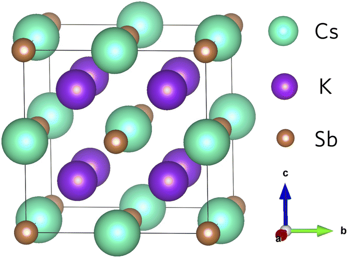 | ||
| Fig. 1 Crystal structure of K2CsSb. Teal, purple, and brown spheres represent Cs, K and Sb atoms, respectively. | ||
To assess the dynamical stability of K2CsSb, we further calculate vibrational properties within the harmonic approximation. The phonon dispersion diagram presented in Fig. S2 of the ESI† reveals the absence of imaginary modes, highlighting the stability of the ground state structure. To investigate the thermodynamic stability of K2CsSb, we employed convex hull analysis to calculate the energy above hull against all competing elemental, secondary, and ternary phases in the Materials Project database. We find the energy above hull above to be zero, indicating that the material is stable with respect to decomposition. Accordingly, our calculations highlight the thermodynamic and dynamical stability of K2CsSb as is also observed in experiments.
Electronic properties
The projected density of states calculated using HSE + SOC is presented in Fig. 2a. The valence band maximum is dominated by Sb 5p states, whereas the conduction band minimum is a mixture of Sb 6s, Cs d, and K d contributions. The orbital projection scheme fails to capture a significant portion of the total density of states in the conduction band. As we shall demonstrate, this is a consequence of a highly delocalised electron density that fills the interatomic voids in the crystal structure and gives rise to very small electron effective masses.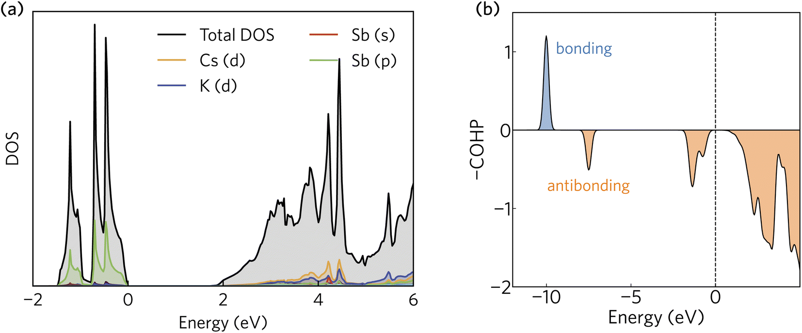 | ||
| Fig. 2 (a) The density of states and (b) crystal orbital Hamilton population (COHP) analysis of K2CsSb calculated using HSE + SOC. In (a) and (b), the valence band maximum has been set to zero eV. | ||
The Sb 5p states at the valence band edge are largely non-bonding in character. This is confirmed through the COHP analysis presented in Fig. 2b, which provides an indication of the type (bonding vs. antibonding) and strength of orbital interactions. Despite a strongly localised peak in the density of states, the COHP analysis reveals a much smaller negative peak at the valence band edge indicating weakly antibonding/non-bonding interactions. This can be rationalised by considering the partial charge density isosurfaces of the valence band maximum presented in Fig. 3a. The isosurface indicates a spherical electron density surrounding the antimony sites (corresponding to the fully filled Sb 5p orbitals), with no other orbital interactions present. The fully filled Sb 5s, K 3p and Cs 5p orbitals are found much deeper inside the valence band and can be considered semicore states (see Fig. S2 in the ESI†). In contrast, the conduction band minimum exhibits strongly antibonding character, as indicated by the large negative peak above the Fermi level in the COHP analysis (Fig. 2b). As can be observed in the partial charge density isosurface of the conduction band minimum, the Sb 6s states are mixed with higher energy unoccupied alkali orbitals to form channels throughout the crystal, resulting in a “sponge” like structure. The obvious lack of charge density between the antimony s states and the almost free electron density between the atoms highlights the antibonding character of these states.
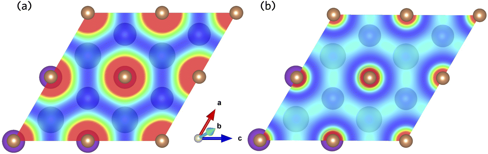 | ||
| Fig. 3 Partial charge density isosurfaces for the (a) valence band maximum and (b) conduction band minimum of K2CsSb calculated using HSE + SOC. | ||
The electronic band structure of K2CsSb, calculated using HSE + SOC, is presented in Fig. 4. The band structure displays a direct band gap of 1.59 eV at the Γ-point, within the ideal range for a photovoltaic absorber between 1.1 and 1.6 eV. We find relatively strong relativistic renormalisation of the band gap (0.183 eV) due to the presence of heavy antimony atoms. The renormalisation mainly originates from the valence band maximum, which is raised by 0.179 eV due to spin splitting. This is considerably larger than seen in other antimony-based absorbers such as Sb2Se3 which exhibits relativistic renormalisation on the order of 0.05 eV.44 We note the calculated band gap is significantly overestimated compared to experiment. Photoconductivity measurements on K2CsSb thin films suggest a band gap of 1.2 eV.14 The origin of this discrepancy is unclear. One possible explanation is the absence of lattice expansion and electron–phonon coupling in our calculations that can act to renormalise the gap. Regardless, our results are in agreement with a recent GW study that reported a band gap of 1.62 eV.9
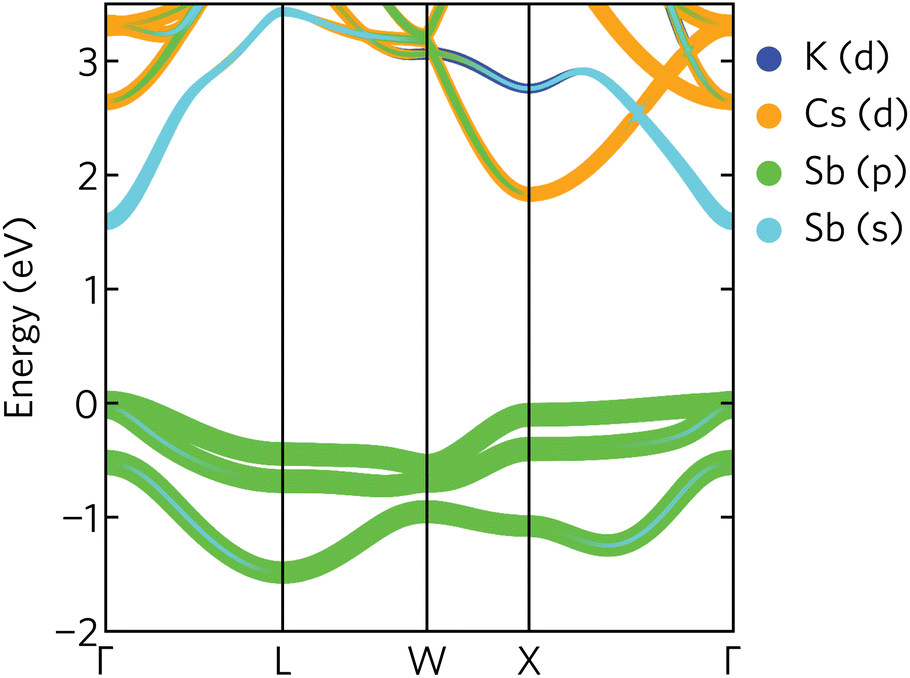 | ||
| Fig. 4 Projected band structure of K2CsSb calculated using HSE + SOC. The valence band maximum is set to zero eV. | ||
The valence band maximum is relatively dispersionless with strong antimony p character (Fig. 4), in agreement with the calculated density of states and partial charge density isosurfaces. In contrast, the conduction band minimum is highly dispersive and largely composed of antimony s character. We also note a secondary conduction band pocket at the X high-symmetry point, with a direct gap of 1.85 eV, only slightly larger than the fundamental gap at Γ. This secondary minimum has mainly Cs d character, with some Sb p mixing away from the band edge.
To better understand the carrier transport properties of K2CsSb, we calculated band edge effective masses using the SUMO package.35 The effective masses of the valence band maximum and conduction band minimum are listed in Table 1. The conduction band minimum exhibits very small electron effective masses of 0.17m0 in both the Γ → L and Γ → X high-symmetry directions. This is comparable to state-of-the-art photovoltaics such as CH3NH3PbI3 (me = 0.15m0)45 and CdTe (0.11m0) and considerably smaller than other Sb-containing absorbers including CuSbSe2 (0.71m0),46 SbSI (0.65m0),47 and Sb2Se3 (∼0.35m0),32 as well as other half-Heuslers such as RuNbSb (0.71m0) and FeNbSb (1.43m0)48 and full-Heusler Fe2VAl (0.60m0).49 The small electron effective masses in K2CsSb originate from the high conduction bandwidth and “sponge” like delocalised nearly free electron density. Small effective masses are beneficial for charge extraction since photoexcited carriers have a greater chance of reaching the contact layers before recombining and generally result in large polarons, weakly bound excitons,50 and small defect capture cross sections.51 The hole effective masses in K2CsSb are noticeably larger, with values of 1.01m0 (along Γ → L) and 0.82m0 (Γ → X). This is similar to other emerging bismuth- and antimony-based absorbers such as BiSI (mh = 0.95m0),52 SbI3 (1.15m0),53 and Sb2Se3 (0.90m0),32 which also display preferential electron transport behaviour.
| Compound | E g (eV) | ε ∞ | ε s | E b (meV) | m e (m0) | m h (m0) | ||
|---|---|---|---|---|---|---|---|---|
| Γ → L | Γ → X | Γ → L | Γ → X | |||||
| K2CsSb | 1.589 | 6.11 | 14.02 | 9.9 | 0.17 | 0.17 | 1.01 | 0.82 |
Optical properties
A large dielectric constant is thought to play a key role in achieving defect tolerance by minimising trap-introduced non-radiative losses within photovoltaic devices.16,54 This is due to the role the dielectric constant plays in the defect capture cross-sections. A large dielectric constant also screens charged impurities preventing defect scattering.55 The high-frequency (ε∞) and static (εs) dielectric constants of K2CsSb were calculated to be 7.91 and 14.0, respectively. The relatively large difference between the two constants indicates that ionic screening due to longitudinal polar optical phonons plays a major role in the dielectric response. Due to the cubic symmetry the dielectric constants are isotropic. The calculated static dielectric constant is considerably smaller than those found in other ns2 containing solar absorbers such as Sb2Se (∼75)32 and CH3NH3PbI3 (80),56 which exhibit very large ionic screening due to the polarisability of the lone pair. However, it is comparable to well-established photovoltaics including silicon (11.7),57 GaAs (12.90),58 and CdTe (10.31).59 We therefore expect a reasonable degree of charge screening will be observed in K2CsSb.The static dielectric constant can be used to calculate the Wannier–Mott exciton radius within effective mass theory as a0 = εs/μ (in au), where the reduced effective mass μ = (memh)/(me + mh). This gives an exciton radius of 52 Å and associated exciton binding energy (Eb = 1/(2εsa0)) of 10 meV. This suggests that excitons will not play a significant role in photovoltaic device physics and are unlikely to be the origin of the discrepancy between the calculated and experimentally measured band gap.
In addition to the appropriate band gap and mobile charge carriers, strong visible light absorption is essential to achieve high photovoltaic efficiency. The optical absorption of K2CsSb, calculated using HSE + SOC, is displayed in Fig. 5a. The absorption displays a steep onset, quickly reaching greater than 105 cm−1 within 0.7 eV of the fundamental bandgap. The sharp onset is competitive with other thin-film absorbers such as CdTe and the hybrid perovskites, and significantly stronger than indirect band gap absorbers such as silicon.60 The strong absorption can be rationalised by the relatively flat valence band which increases the joint density of states near the fundamental gap. Furthermore, as detailed above, the secondary conduction band pocket at X will result in additional absorption at photon energies above 1.85 eV.
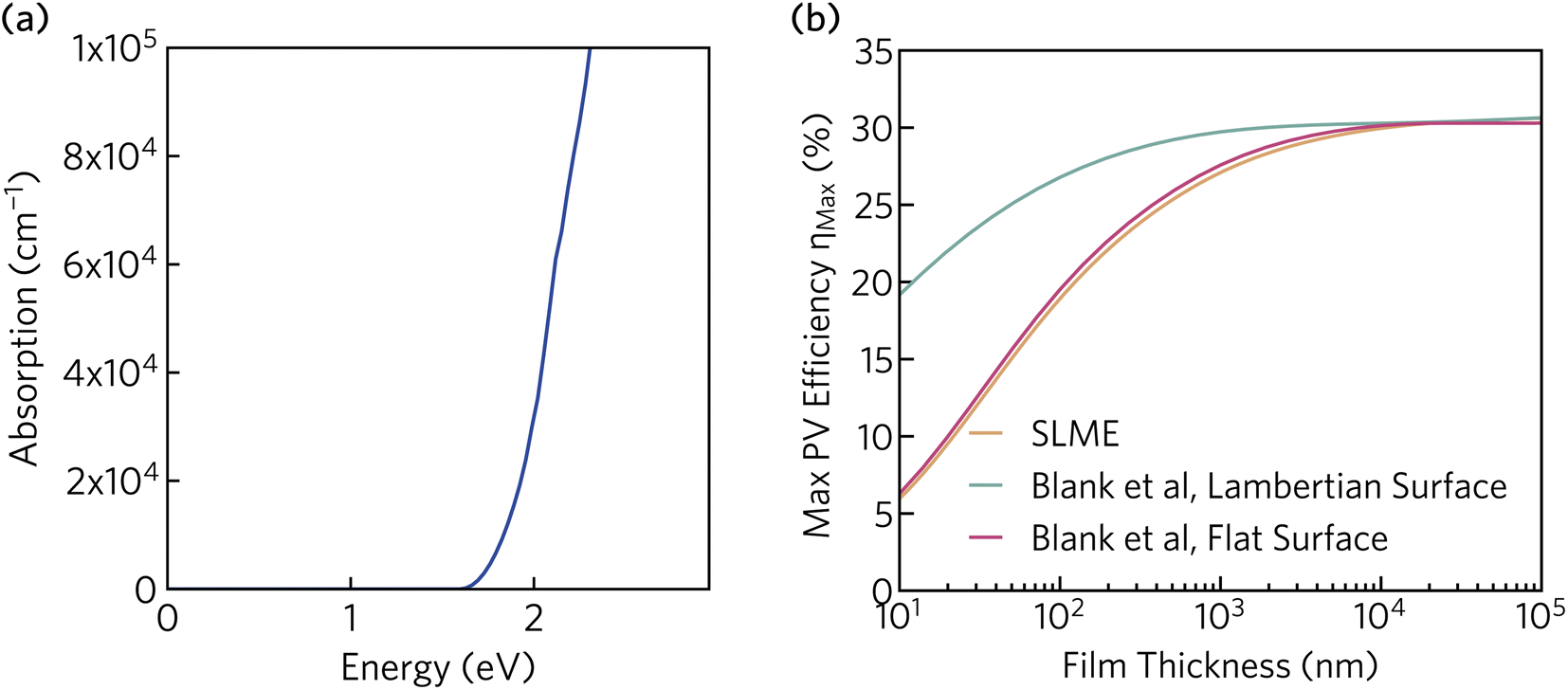 | ||
| Fig. 5 (a) Optical absorption spectrum of K2CsSb calculated using HSE + SOC. (b) Thickness-dependent theoretical maximum efficiency of K2CsSb calculated using the “spectroscopic limited maximum efficiency” (SLME) method and detailed balance metric proposed by Blank et al.40 | ||
To evaluate the potential for K2CsSb in photovoltaic applications, we calculated the thickness-dependent conversion efficiency using the “spectroscopic limited maximum efficiency” (SLME) model39 and the detailed balance metric proposed by Blank et al.40 The Blank approach extends the SLME metric by distinguishing the external luminescence yield from internal radiative recombination, with more details of this approach given in Section S7 of the ESI.† Both approaches used the frequency-dependent dielectric response calculated using HSE + SOC. The theoretical efficiency is strongly dependent on the thickness of the absorber layer, with the maximum efficiency reaching a plateau of 30% at a thickness of 10 μm. The Lambertian model reduces losses by simulating unity reflectance for the back surface and a diffusely scattering front surface, and exhibits higher efficiencies than both SLME and a flat surface for the same film thickness. At a thickness of 200 nm (appropriate for thin-film photovoltaics), the maximum efficiency is found to be over 28%. This is considerably larger than those predicted for Sb2Se3 and NaSbS2 at the same film thickness (∼10% (ref. 32) and 22.3%,61 respectively) and comparable to those of other emerging absorbers such as Sn2SbS2I3 (∼29%).33 We stress that these metrics provide an upper limit to the theoretical efficiency and do not take into account voltage losses due to non-radiative recombination and resistive interfaces. Regardless, these results highlight the potential for K2CsSb as an absorber layer in photovoltaic devices.
Band alignment
To provide recommendations on the ideal device architecture of K2CsSb devices, we performed band alignment calculations using a slab–vacuum model. An efficient band alignment between electron and hole contact layers can minimise barriers for carrier diffusion at interfaces and prevent open-circuit voltage losses. We note our calculations provide estimates of the “bulk” band alignment, and do not take into account relaxations and band bending at the surface. We calculate an ionisation potential and electron affinity of 1.82 eV and 3.42 eV, respectively. Our results differ somewhat from early experimental reports on K2CsSb that observed an electron affinity of 1.1 eV through photoconductivity measurements.62 The origin of this discrepancy is unclear, but could result from the relatively thin films used or reconstruction at the surface. Furthermore, our calculated results are for the bulk electronic structure, whereas experimental measurements will depend on the surface termination of the crystal. Regardless, these relatively small values mean that photons with energies greater than the ionisation potential could cause the emission of electrons through the photoelectric effect, preventing carrier collection at the device contacts. To simulate the impact on the internal quantum efficiency due to photoemitted carriers, we perform the SLME metric with the absorption greater than the ionisation potential set to zero. We find very little change in the predicted theoretical efficiencies (less than 1%, see Fig. S5 in the ESI†). This can be rationalised since high-energy ultraviolet photons contribute a vanishing portion of the AM 1.5 solar spectrum. Accordingly, the impact of the small ionisation potential of photovoltaic performance is expected to be limited.In Fig. 6, we compare the band alignment of K2CsSb to a range of conventional and emerging photovoltaic absorbers. We find the electron affinity and ionisation potential of K2CsSb to be much smaller than those of any other commonly used absorber.67,68 For example, the ionisation potential of K2CsSb is smaller than the electron affinity of both Si and AgCuS. The origin of the small ionisation potentials can be explained by the electronic configuration of antimony. In K2CsSb, the 5p orbitals are fully occupied and form the valence band maximum, whereas in other common absorbers, the valence p states are either fully unoccupied (thereby forming the conduction band) or covalently bonded to give occupied bonding states and unoccupied antibonding states (the latter of which forms the conduction band).
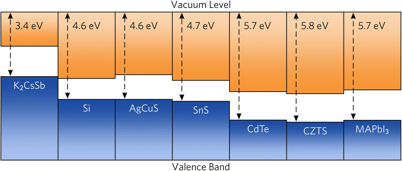 | ||
| Fig. 6 Calculated band alignment of K2CsSb compared to conventional and emerging photovoltaic absorbers. Electron affinity and bandgap data were taken from ref. 63–66. | ||
The low ionisation potential and electron affinity of K2CsSb will require judicious choice of contact materials to maximise the obtainable open-circuit voltage. For favourable electron transport throughout a device, the work function (Φ) of the transparent electron contact should be greater than the electron affinity of the absorber. Conversely, the work function of the hole contact layer should be smaller than the absorber's ionisation potential. Commonly used n-type transparent conductors have significantly deeper work functions (greater than 4 eV) and will not be appropriate for use with K2CsSb. Accordingly, use of an ultralow work function n-type contact, such as the semiconducting polymer TPHP(LiClO4) (Φ = 2.2 eV), will be necessary.69 For the hole transport layer, a small work function metal alloy such as MgNd (Φ = 3.5 eV) may be appropriate,70 although other contacts without expensive Nd would be preferred.
Conclusion
We have proposed K2CsSb as a potential photovoltaic candidate based on relativistic density functional theory calculations. K2CsSb possesses an ideal band gap of 1.59 eV, very small electron effective mass (0.17m0), small predicted exciton binding energies, and strong optical absorption across the entire visible spectrum. We have highlighted the origin of the favourable electronic properties is a highly delocalised “sponge”-like electron density in the conduction band. The predicted maximum theoretical efficiency of 28% for a 200 nm thin film is competitive with other state-of-the-art absorbers. Furthermore, we performed band alignment calculations to provide suggestions for an optimised device architecture that can maximise open-circuit voltages. We believe K2CsSb is a promising candidate photovoltaic absorber worthy of further study.Author contributions
Ruiqi Wu: investigation, formal analysis, methodology, visualization, writing – original draft, writing – review & editing. Alex Ganose: conceptualization, methodology, resources, supervision, writing – review & editing.Conflicts of interest
There are no conflicts to declare.Acknowledgements
A. M. G. was supported by EPSRC Fellowship EP/T033231/1. We are grateful to the UK Materials and Molecular Modelling Hub for computational resources, which is partially funded by EPSRC (EP/P020194/1 and EP/T022213/1). This work used the ARCHER2 UK National Supercomputing Service (https://www.archer2.ac.uk) via our membership of the UK's HEC Materials Chemistry Consortium, which is funded by EPSRC (EP/L000202).References
- IEA, Renewable Electricity – Analysis, https://www.iea.org/reports/renewable-electricity, 2021 Search PubMed.
- D. S. Philipps, F. Ise, W. Warmuth and P. P. GmbH, Photovoltaics Report, 2022 Search PubMed.
- Deutsche Physikalische Gesellschaft (1899-1945), Verhandlungen der Deutschen physikalischen Gesellschaft; Friedr. Vieweg & Sohn, 1903 Search PubMed.
- P. D. Patel, S. B. Pillai, S. M. Shinde, S. D. Gupta and P. K. Jha, Electronic, Magnetic, Thermoelectric and Lattice Dynamical Properties of Full Heusler Alloy Mn2RhSi: DFT Study, Phys. B, 2018, 550, 376–382 CrossRef CAS.
- F. Gucci, T. G. Saunders, B. Srinivasan, F. Cheviré, D. A. Ferluccio, J.-W. G. Bos and M. J. Reece, Hybrid Flash-SPS of TiNiCu0.05Sn with Reduced Thermal Conductivity, J. Alloys Compd., 2020, 837, 155058 CrossRef CAS.
- C. S. Lue, C. F. Chen, J. Y. Lin, Y. T. Yu and Y. K. Kuo, Thermoelectric Properties of Quaternary Heusler Alloys Fe2VAl1−xSix, Phys. Rev. B: Condens. Matter Mater. Phys., 2007, 75, 064204 CrossRef.
- L. Guo, M. Kuriki, A. Yokota, M. Urano and K. Negishi, Substrate Dependence of CsK2Sb Photo-Cathode Performance, Prog. Theor. Phys., 2017, 2017, 033G01 Search PubMed.
- M. A. Mamun, C. Hernandez-Garcia, M. Poelker and A. A. Elmustafa, Correlation of CsK2Sb Photocathode Lifetime with Antimony Thickness, APL Mater., 2015, 3, 066103 CrossRef.
- C. Cocchi, S. Mistry, M. Schmeißer, J. Kühn and T. Kamps, First-Principles Many-Body Study of the Electronic and Optical Properties of CsK2Sb, a Semiconducting Material for Ultra-Bright Electron Sources, J. Phys.: Condens. Matter, 2018, 31, 014002 CrossRef PubMed.
- G. Xing, J. Sun, Y. Li, X. Fan, W. Zheng and D. J. Singh, Electronic Fitness Function for Screening Semiconductors as Thermoelectric Materials, Phys. Rev. Mater., 2017, 1, 065405 CrossRef.
- K. Yuan, X. Zhang, Z. Chang, D. Tang and M. Hu, Antibonding Induced Anharmonicity Leading to Ultralow Lattice Thermal Conductivity and Extraordinary Thermoelectric Performance in CsK2X (X = Sb, Bi), J. Mater. Chem. C, 2022, 10, 15822–15832 RSC.
- T. Yue, P. Sui, Y. Zhao, J. Ni, S. Meng and Z. Dai, Theoretical Prediction of Mechanics, Transport, and Thermoelectric Properties of Full Heusler Compounds Na2KSb and X2CsSb (X = K, Rb), Phys. Rev. B, 2022, 105, 184304 CrossRef CAS.
- M. Gaowei, Z. Ding, S. Schubert, H. B. Bhandari, J. Sinsheimer, J. Kuehn, V. V. Nagarkar, M. S. J. Marshall, J. Walsh, E. M. Muller, K. Attenkofer, H. J. Frisch, H. Padmore and J. Smedley, Synthesis and X-Ray Characterization of Sputtered Bi-Alkali Antimonide Photocathodes, APL Mater., 2017, 5, 116104 CrossRef.
- C. Ghosh and B. P. Varma, Preparation and Study of Properties of a Few Alkali Antimonide Photocathodes, J. Appl. Phys., 1978, 49, 4549 CrossRef CAS.
- J. M. Frost, L. D. Whalley and A. Walsh, Slow Cooling of Hot Polarons in Halide Perovskite Solar Cells, ACS Energy Lett., 2017, 2, 2647–2652 CrossRef CAS PubMed.
- A. M. Ganose, C. N. Savory and D. O. Scanlon, Beyond Methylammonium Lead Iodide: Prospects for the Emergent Field of ns2 Containing Solar Absorbers, Chem. Commun., 2016, 53, 20–44 RSC.
- Y. Zhao, S. Wang, C. Li, B. Che, X. Chen, H. Chen, R. Tang, X. Wang, G. Chen, T. Wang, J. Gong, T. Chen, X. Xiao and J. Li, Regulating Deposition Kinetics via a Novel Additive-Assisted Chemical Bath Deposition Technology Enables Fabrication of 10.57%-Efficiency Sb2Se3 Solar Cells, Energy Environ. Sci., 2022, 15, 5118–5128 RSC.
- A. Walsh, D. J. Payne, R. G. Egdell and G. W. Watson, Stereochemistry of Post-Transition Metal Oxides: Revision of the Classical Lone Pair Model, Chem. Soc. Rev., 2011, 40, 4455–4463 RSC.
- X. Wang, S. R. Kavanagh, D. O. Scanlon and A. Walsh, Four-Electron Negative-U Vacancy Defects in Antimony Selenide, arXiv, 2023, preprint, arXiv:2302.04901, DOI:10.48550/arXiv.2302.04901.
- W. Kohn and L. J. Sham, Self-Consistent Equations Including Exchange and Correlation Effects, Phys. Rev., 1965, 140, A1133–A1138 CrossRef.
- G. Kresse and J. Hafner, Ab Initio Molecular Dynamics for Liquid Metals, Phys. Rev. B: Condens. Matter Mater. Phys., 1993, 47, 558–561 CrossRef CAS PubMed.
- G. Kresse and J. Furthmüller, Efficient Iterative Schemes for Ab Initio Total-Energy Calculations Using a Plane-Wave Basis Set, Phys. Rev. B: Condens. Matter Mater. Phys., 1996, 54, 11169–11186 CrossRef CAS PubMed.
- G. Kresse and J. Hafner, Ab Initio Molecular-Dynamics Simulation of the Liquid-Metal–Amorphous-Semiconductor Transition in Germanium, Phys. Rev. B: Condens. Matter Mater. Phys., 1994, 49, 14251–14269 CrossRef CAS PubMed.
- G. Kresse and J. Furthmüller, Efficiency of Ab Initio Total Energy Calculations for Metals and Semiconductors Using a Plane-Wave Basis Set, Comput. Mater. Sci., 1996, 6, 15–50 CrossRef CAS.
- G. Kresse and D. Joubert, From Ultrasoft Pseudopotentials to the Projector Augmented-Wave Method, Phys. Rev. B: Condens. Matter Mater. Phys., 1999, 59, 1758–1775 CrossRef CAS.
- J. P. Perdew, A. Ruzsinszky, G. I. Csonka, O. A. Vydrov, G. E. Scuseria, L. A. Constantin, X. Zhou and K. Burke, Restoring the Density-Gradient Expansion for Exchange in Solids and Surfaces, Phys. Rev. Lett., 2008, 100, 136406 CrossRef PubMed.
- J. P. Perdew, K. Burke and M. Ernzerhof, Generalized Gradient Approximation Made Simple, Phys. Rev. Lett., 1996, 77, 3865–3868 CrossRef CAS PubMed.
- A. V. Krukau, O. A. Vydrov, A. F. Izmaylov and G. E. Scuseria, Influence of the Exchange Screening Parameter on the Performance of Screened Hybrid Functionals, J. Chem. Phys., 2006, 125, 224106 CrossRef PubMed.
- J. Heyd, G. E. Scuseria and M. Ernzerhof, Hybrid Functionals Based on a Screened Coulomb Potential, J. Chem. Phys., 2003, 118, 8207–8215 CrossRef CAS.
- J.-H. Pöhls, S. Chanakian, J. Park, A. M. Ganose, A. Dunn, N. Friesen, A. Bhattacharya, B. Hogan, S. Bux, A. Jain, A. Mar and A. Zevalkink, Experimental validation of high thermoelectric performance in RECuZnP2 predicted by high-throughput DFT calculations, Mater. Horiz., 2021, 8, 209–215 RSC.
- W. Travis, C. E. Knapp, C. N. Savory, A. M. Ganose, P. Kafourou, X. Song, Z. Sharif, J. K. Cockcroft, D. O. Scanlon, H. Bronstein and R. G. Palgrave, Hybrid Organic–Inorganic Coordination Complexes as Tunable Optical Response Materials, Inorg. Chem., 2016, 55, 3393–3400 CrossRef CAS PubMed.
- X. Wang, Z. Li, S. R. Kavanagh, A. M. Ganose and A. Walsh, Lone Pair Driven Anisotropy in Antimony Chalcogenide Semiconductors, Phys. Chem. Chem. Phys., 2022, 24, 7195–7202 RSC.
- S. R. Kavanagh, C. N. Savory, D. O. Scanlon and A. Walsh, Hidden Spontaneous Polarisation in the Chalcohalide Photovoltaic Absorber Sn2SbS2I3, Mater. Horiz., 2021, 8, 2709–2716 RSC.
- A. M. Ganose, S. Matsumoto, J. Buckeridge and D. O. Scanlon, Defect Engineering of Earth-Abundant Solar Absorbers BiSI and BiSeI, Chem. Mater., 2018, 30, 3827–3835 CrossRef CAS PubMed.
- M. G. Alex, J. J. Adam and O. S. David, Sumo: Command-line Tools for Plotting and Analysis of Periodic Ab Initio Calculations, J. Open Source Softw., 2018, 3, 717 CrossRef.
- R. Dronskowski and P. E. Bloechl, Crystal Orbital Hamilton Populations (COHP): Energy-Resolved Visualization of Chemical Bonding in Solids Based on Density-Functional Calculations, J. Phys. Chem., 1993, 97, 8617–8624 CrossRef CAS.
- M. Gajdoš, K. Hummer, G. Kresse, J. Furthmüller and F. Bechstedt, Linear Optical Properties in the Projector-Augmented Wave Methodology, Phys. Rev. B: Condens. Matter Mater. Phys., 2006, 73, 045112 CrossRef.
- C. Lian, Z. A. Ali, H. Kwon and B. M. Wong, Indirect but Efficient: Laser-Excited Electrons Can Drive Ultrafast Polarization Switching in Ferroelectric Materials, J. Phys. Chem. Lett., 2019, 10, 3402–3407 CrossRef CAS PubMed.
- L. Yu and A. Zunger, Identification of Potential Photovoltaic Absorbers Based on First-Principles Spectroscopic Screening of Materials, Phys. Rev. Lett., 2012, 108, 068701 CrossRef PubMed.
- B. Blank, T. Kirchartz, S. Lany and U. Rau, Selection Metric for Photovoltaic Materials Screening Based on Detailed-Balance Analysis, Phys. Rev. Appl., 2017, 8, 024032 CrossRef.
- K. Brlec, D. W. Davies and D. O. Scanlon, Surfaxe: Systematic Surface Calculations, J. Open Source Softw., 2021, 6, 3171 CrossRef.
- A. Togo, First-Principles Phonon Calculations with Phonopy and Phono3py, J. Phys. Soc. Jpn., 2023, 92, 012001 CrossRef.
- Heusler Alloys: Properties, Growth, Applications, ed. Felser, C. and Hirohata, A., Springer Series in Materials Science, Springer International Publishing, Cham, 2016, vol. 222 Search PubMed.
- C. N. Savory and D. O. Scanlon, The Complex Defect Chemistry of Antimony Selenide, J. Mater. Chem. A, 2019, 7, 10739–10744 RSC.
- J. M. Frost, K. T. Butler, F. Brivio, C. H. Hendon, M. van Schilfgaarde and A. Walsh, Atomistic Origins of High-Performance in Hybrid Halide Perovskite Solar Cells, Nano Lett., 2014, 14, 2584–2590 CrossRef CAS PubMed.
- A. W. Welch, L. L. Baranowski, H. Peng, H. Hempel, R. Eichberger, T. Unold, S. Lany, C. Wolden and A. Zakutayev, Trade-Offs in Thin Film Solar Cells with Layered Chalcostibite Photovoltaic Absorbers, Adv. Energy Mater., 2017, 7, 1601935 CrossRef.
- Y. C. Choi, E. Hwang and D.-H. Kim, Controlled Growth of SbSI Thin Films from Amorphous Sb2S3 for Low-Temperature Solution Processed Chalcohalide Solar Cells, APL Mater., 2018, 6, 121108 CrossRef.
- T. Fang, S. Zheng, T. Zhou, L. Yan and P. Zhang, Computational prediction of high thermoelectric performance in p-type half-Heusler compounds with low band effective mass, Phys. Chem. Chem. Phys., 2017, 19, 4411–4417 RSC.
- B. Hinterleitner, F. Garmroudi, N. Reumann, T. Mori, E. Bauer and R. Podloucky, The electronic pseudo band gap states and electronic transport of the full-Heusler compound Fe2VAl, J. Mater. Chem. C, 2021, 9, 2073–2085 RSC.
- A. Walsh and A. Zunger, Instilling Defect Tolerance in New Compounds, Nat. Mater., 2017, 16, 964–967 CrossRef CAS PubMed.
- Y. Huang, H. Yuan and H. Chen, High-Performance Thermoelectrics in Two-Dimensional Layered AB2Te4 (A = Sn, Pb; B = Sb, Bi) Ternary Compounds, Phys. Chem. Chem. Phys., 2022, 1808–1818 Search PubMed.
- D. Tiwari, F. Cardoso-Delgado, D. Alibhai, M. Mombrú and D. J. Fermín, Photovoltaic Performance of Phase-Pure Orthorhombic BiSI Thin-Films, ACS Appl. Energy Mater., 2019, 2, 3878–3885 CrossRef CAS.
- P. Liu, F. Lu, M. Wu, X. Luo, Y. Cheng, X.-W. Wang, W. Wang, W.-H. Wang, H. Liu and K. Cho, Electronic Structures and Band Alignments of Monolayer Metal Trihalide Semiconductors MX3, J. Mater. Chem. C, 2017, 5, 9066–9071 RSC.
- R. Su, Z. Xu, J. Wu, D. Luo, Q. Hu, W. Yang, X. Yang, R. Zhang, H. Yu, T. P. Russell, Q. Gong, W. Zhang and R. Zhu, Dielectric Screening in Perovskite Photovoltaics, Nat. Commun., 2021, 12, 2479 CrossRef CAS PubMed.
- A. M. Ganose, J. Park, A. Faghaninia, R. Woods-Robinson, K. A. Persson and A. Jain, Efficient Calculation of Carrier Scattering Rates from First Principles, Nat. Commun., 2021, 12, 2222 CrossRef CAS PubMed.
- S. Govinda, B. P. Kore, M. Bokdam, P. Mahale, A. Kumar, S. Pal, B. Bhattacharyya, J. Lahnsteiner, G. Kresse, C. Franchini, A. Pandey and D. D. Sarma, Behavior of Methylammonium Dipoles in MAPbX3 (X = Br and I), J. Phys. Chem. Lett., 2017, 8, 4113–4121 CrossRef CAS PubMed.
- W. C. Dunlap and R. L. Watters, Direct Measurement of the Dielectric Constants of Silicon and Germanium, Phys. Rev., 1953, 92, 1396–1397 CrossRef CAS.
- W. J. Moore and R. T. Holm, Infrared Dielectric Constant of Gallium Arsenide, J. Appl. Phys., 1996, 80, 6939–6942 CrossRef CAS.
- I. Strzalkowski, S. Joshi and C. R. Crowell, Dielectric Constant and Its Temperature Dependence for GaAs, CdTe, and ZnSe, Appl. Phys. Lett., 1976, 28, 350–352 CrossRef CAS.
- S. De Wolf, J. Holovsky, S.-J. Moon, P. Löper, B. Niesen, M. Ledinsky, F.-J. Haug, J.-H. Yum and C. Ballif, Organometallic Halide Perovskites: Sharp Optical Absorption Edge and Its Relation to Photovoltaic Performance, J. Phys. Chem. Lett., 2014, 5, 1035–1039 CrossRef CAS PubMed.
- W. W. W. Leung, C. N. Savory, R. G. Palgrave and D. O. Scanlon, An Experimental and Theoretical Study into NaSbS2 as an Emerging Solar Absorber, J. Mater. Chem. C, 2019, 7, 2059–2067 RSC.
- R. Nathan and C. H. B. Mee, Photoelectric and Related Properties of the Potassium—Antimony—Caesium Photocathode, Int. J. Electron., 1967, 23, 349–354 CrossRef CAS.
- L. A. Burton and A. Walsh, Band Alignment in SnS Thin-Film Solar Cells: Possible Origin of the Low Conversion Efficiency, Appl. Phys. Lett., 2013, 102, 132111 CrossRef.
- J. Brgoch, A. J. Lehner, M. Chabinyc and R. Seshadri, Ab Initio Calculations of Band Gaps and Absolute Band Positions of Polymorphs of RbPbI3 and CsPbI3: Implications for Main-Group Halide Perovskite Photovoltaics, J. Phys. Chem. C, 2014, 118, 27721–27727 CrossRef CAS.
- C. N. Savory, A. M. Ganose, W. Travis, R. S. Atri, R. G. Palgrave and D. O. Scanlon, An Assessment of Silver Copper Sulfides for Photovoltaic Applications: Theoretical and Experimental Insights, J. Mater. Chem. A, 2016, 4, 12648–12657 RSC.
- A. Walsh, Principles of Chemical Bonding and Band Gap Engineering in Hybrid Organic–Inorganic Halide Perovskites, J. Phys. Chem. C, 2015, 119, 5755–5760 CrossRef CAS PubMed.
- T. J. Whittles, L. A. Burton, J. M. Skelton, A. Walsh, T. D. Veal and V. R. Dhanak, Band Alignments, Valence Bands, and Core Levels in the Tin Sulfides SnS, SnS2, and Sn2S3: Experiment and Theory, Chem. Mater., 2016, 28, 3718–3726 CrossRef CAS.
- G. Teeter, X-Ray and Ultraviolet Photoelectron Spectroscopy Measurements of Cu-doped CdTe(111)-B: Observation of Temperature-Reversible CuxTe Precipitation and Effect on Ionization Potential, J. Appl. Phys., 2007, 102, 034504 CrossRef.
- B. Tong, J. Du, L. Yin, D. Zhang, W. Zhang, Y. Liu, Y. Wei, C. Liu, Y. Liang, D.-M. Sun, L.-P. Ma, H.-M. Cheng and W. Ren, A Polymer Electrolyte Design Enables Ultralow-Work-Function Electrode for High-Performance Optoelectronics, Nat. Commun., 2022, 13, 4987 CrossRef CAS PubMed.
- K. Ge, J. Chen, B. Chen, Y. Shen, J. Guo, F. Li, H. Liu, Y. Xu and Y. Mai, Low Work Function Intermetallic Thin Film as a Back Surface Field Material for Hybrid Solar Cells, Sol. Energy, 2018, 162, 397–402 CrossRef CAS.
Footnote |
| † Electronic supplementary information (ESI) available. See DOI: https://doi.org/10.1039/d3ta02061d |
| This journal is © The Royal Society of Chemistry 2023 |