DOI:
10.1039/D2TA09967E
(Review Article)
J. Mater. Chem. A, 2023,
11, 5427-5459
One-dimensional III-nitrides: towards ultrahigh efficiency, ultrahigh stability artificial photosynthesis
Received
23rd December 2022
, Accepted 9th February 2023
First published on 28th February 2023
Abstract
The depletion of carbon-based fuels and emerging environmental problems are more than ever driving the demand for green energy sources. Artificial photosynthesis demonstrated by catalytically active semiconductors can convert solar energy into storable energy sources such as hydrogen and carbon products by water splitting and carbon dioxide reduction reaction, respectively. Semiconductors with one-dimensional (1D) nanostructures have gained tremendous attention due to their large surface area and enhanced light absorption. However, semiconductor nanostructures suffer from degradation caused by oxidation, corrosion, and undesirable changes in morphology during reaction in aqueous electrolytes. In this review, 1D nanostructured III-nitrides are introduced to offer a comprehensive overview of their synthesis methods, unique structural, electronic, optical, surface, and catalytic properties, as well as their efficiency, and stability for artificial photosynthesis. Band gap engineering and tandem stacking of 1D III-nitrides for broadband light absorption are highlighted. Recent findings on the inherent catalytic activity and stability of 1D III-nitrides are presented. Furthermore, this paper summarizes the ability of cocatalysts integrated on 1D III-nitrides to overcome the performance bottlenecks of water splitting and CO2 reduction reactions. Finally, the challenges of 1D III-nitrides for practical application of photo(electro)chemical reactions and prospective insights for future development are provided.
 Wan Jae Dong | Dr Wan Jae Dong received his B.S. degree in Materials Science and Engineering from Korea University (South Korea) in 2010. He completed his M.S. (2012) and Ph.D. (2016) degrees in Materials Science and Engineering Department from POSTECH (South Korea). He is currently Assistant Research Scientist in University of Michigan (USA). His research interest focuses on artificial photosynthesis including water splitting, CO2 conversion, NH3 synthesis, and C–N coupling. |
 Zetian Mi | Zetian Mi is a Professor at the University of Michigan. His teaching and research interests are in the areas of low dimensional semiconductors and their applications in photonic, electronic, artificial photosynthesis, and quantum devices. He has received the Science and Engineering Award from W. M. Keck Foundation, the David E. Liddle Research Excellence Award, and the IEEE Photonics Society Distinguished Lecturer Award. He currently serves as the Editor-in-Chief of Progress in Quantum Electronics, Serial Editor of Semiconductors and Semimetals, and Vice President for Conferences of the IEEE Photonics Society. Mi is a fellow of IEEE, APS, Optica, and SPIE. |
1. Introduction
A massive amount of energy is consumed to maintain daily human life and most of the energy depends on fossil fuels such as petroleum, coal, and natural gas. However, the depletion of fossil fuels propel the cost of energy and emerging environmental issues, which are driving the demand for green energy technology. In this regard, hydrogen (H2) fuel has attracted a lot of attention as an alternative future energy source because high-purity H2 gas can be produced from earth-abundant water resources with zero greenhouse gas emissions.1,2 Along with alternative H2 fuels, carbon dioxide (CO2) recycling is being extensively studied as a future energy technology.3,4 CO2, the main cause of global warming, can be converted into value-added chemicals through catalytic reactions. Inspired by photosynthesis, which transforms CO2 and H2O into hydrocarbons using solar energy in the natural carbon cycle, artificial photosynthetic devices have been developed to convert solar energy to H2 fuel or carbon-based chemicals using CO2 and H2O.5–9 Up to now, efficient artificial photosynthetic devices for H2 production and CO2 recycling have been demonstrated by the integration of semiconductors and cocatalysts. In this configuration, semiconductor materials absorb the light and excite photogenerated electrons and holes into conduction and valence bands, respectively. The photogenerated charge carriers then separate and migrate to the cocatalyst surface to participate in redox reactions. Therefore, artificial photosynthetic devices must overcome the technical challenges of limited light absorption, inefficient charge carrier separation/transfer, and low catalytic activity before they can be put to practical use.
Over past decades, the rapid development of nanotechnology has enabled the fabrication of nanostructured semiconductors in 1-dimensional (1D) morphology, including nanowires, nanorods, and nanofibers.10 These 1D semiconductors have shown distinct physical and chemical characteristics different from their planar counterparts. The large surface-to-volume ratio of 1D nanostructures promotes surface chemical reactions by providing many catalytically active sites.11 New crystal orientations, which are difficult to obtain in planar structures, have been exposed to the surface and boosted catalytic reactions.12 Nanostructures have enhanced light absorption by suppressing Fresnel reflection and by scattering the incident light.13,14 In addition, charge carrier separation and transfer have become much easier since the diffusion lengths of charge carriers have been shortened from the microscale to the nanoscale.15 These advantages of 1D semiconductors have demonstrated much enhanced photoelectrochemical and photocatalytic performance compared to planar structures.16–18 However, there are still many challenges remaining, such as inefficient light absorption, poor stability, and sluggish kinetics of surface chemical reactions. To mitigate these problems, 1D III-nitrides (i.e., GaN, InN, and their alloys) have emerged as next-generation artificial photosynthetic semiconductors.
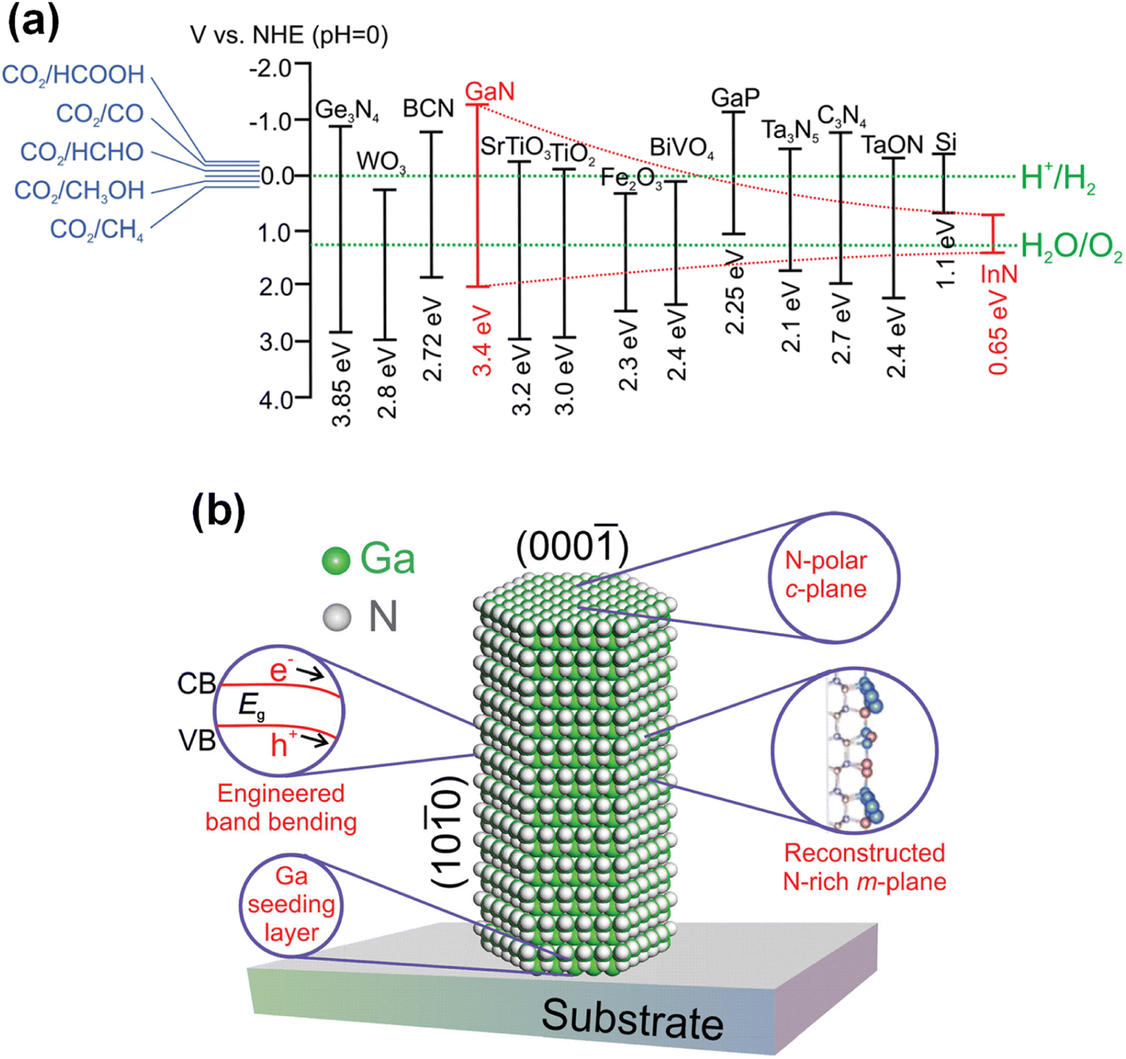
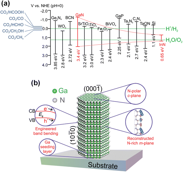
III-Nitrides have been designed and tailored for application in each particular photo(electro)chemical system. Ternary alloying (InGaN) of III-nitrides could allow fine-tuning of the band gap and lattice parameters to access ideal band edge positions and to realize epitaxial growth of high-quality crystals. The energy band gap of III-nitrides can be controlled across nearly the entire solar spectrum while straddling a broad range of redox potentials (Fig. 1a).19–21 Hence, charge carrier transport at the III-nitride/electrolyte interface is energetically feasible for water splitting and CO2 reduction reactions. III-Nitrides typically have a wurtzite crystal structure with a polar c-plane. Since the polarity of III-nitrides leads to the preferential growth of planar film along the c-axis, the catalytic activity of the polar c-plane has been commonly studied for artificial photosynthesis. However, 1D III-nitrides, having a small portion of polar top surface and abundant nonpolar side surfaces, have enabled crystal facet engineering to improve the performance of photoelectrodes and photocatalysts. Each crystal orientation of III-nitrides has different surface electronic structure, surface potential, and catalytic activity. Thus, various optoelectronic and catalytic characteristics can be demonstrated by fabricating III-nitride nanostructures. Moreover, the surface band bending and electrical conductivity of 1D III-nitrides can be manipulated by n- or p-type doping for each particular artificial photosynthetic application.19 Optimized surface band bending has promoted charge carrier separation in semiconductors, which can suppress charge carrier recombination. Interestingly, their surfaces can be terminated with nitrogen atoms, or nitrogen-rich nanoclusters, to protect against photo-corrosion and oxidation, resulting in unprecedented long-term stability (Fig. 1b).22 Hence, 1D III-nitrides show grand promise in promoting H2 production by solar water splitting and CO2 upgrading by a solar-driven CO2 reduction reaction.
 |
| | Fig. 1 (a) Schematic of the tunable InxGa1−xN band structure compared to other semiconductors, including the redox potentials of water splitting and CO2 reduction. Reproduced with permission from ref. 19. Copyright (2016) Royal Society of Chemistry. (b) Schematic of the atomic and electronic structure of nitrogen-terminated GaN nanowire. Reproduced with permission from ref. 22. Copyright (2016) John Wiley and Sons. | |
In this review, the fabrication methods of 1D III-nitride nanostructures are first presented. Then, recent progress in band engineering, doping, and the heterostructures of 1D III-nitride semiconductors for artificial photosynthetic applications is described. Material design strategies for enhancing catalytic reactions are classified into four parts of photoelectrochemical water splitting, photocatalytic water splitting, photoelectrochemical CO2 reduction, and photocatalytic CO2 conversion. Finally, the critical challenges and prospects of 1D III-nitride materials for realizing practical artificial photosynthesis are discussed.
2. Fabrication of 1-dimensional III-nitrides
One-dimensional III-nitride nanostructures have been fabricated by bottom-up growth or top-down etching methods (Fig. 2). In more detail, the growth strategies of 1D III-nitrides can be classified into catalyst-assisted or catalyst-free growth. The top-down methods can also be divided into dry or wet etching processes. In addition, a chemical synthetic method has demonstrated the growth of GaN nanowires using a solution-based synthesis of gallium oxide nanowires followed by nitridation under an NH3 atmosphere.23–26 However, GaN nanowires in powder form, obtained by chemical synthesis, have many crystal defects and charge carrier trapping sites within the band gap, so there is a limit to their application to photoelectrodes. Thus, in the following sections, bottom-up growth and top-down methods for the fabrication of high-crystal-quality 1D III-nitrides are mainly described.
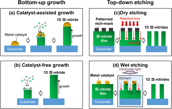 |
| | Fig. 2 Schematic illustrations of representative 1D III-nitride fabrication methods. Bottom-up growth can be classified into (a) catalyst-assisted growth and (b) catalyst-free growth. Top-down etching methods can be classified into (c) dry etching and (d) wet etching. | |
2.1. Bottom-up growth
To date, most high-performing 1D III-nitride nanostructure photoelectrodes or photocatalysts have been fabricated based on the bottom-up method because this process offers high crystal quality with fewer defects. Moreover, tuning of morphology, incorporation of dopants, and constructing heterogeneous structures can be realized by varying the growth parameters, including the temperature, ratio of source materials, and growth duration. Previously, a vapor–liquid–solid growth mechanism was proposed for growing Si whiskers with Au catalysts.27 At high temperature, sufficient to form Si:Au liquid droplets, the Si vapor preferentially incorporates into liquid metal catalysts and nucleates at the interface between Si crystals and liquid droplets, thereby resulting in high-quality Si crystal growth along the axial direction. Eventually, the Au catalyst droplets remain at the top of the Si whiskers. Because the liquid metal catalysts are preferential sites for the incorporation of vapor-phase Si, the morphology and composition of Si whiskers are determined, to a large extent, by the metal catalyst. This metal-catalyst-assisted vapor–liquid–solid growth technique has been extended to the growth of 1D III-nitride semiconductors (Fig. 2a). III-Nitride nanowires, grown by the metal–organic chemical vapor deposition (MOCVD) method, have been successfully fabricated with various catalysts such as Au,28–30 Ni,31–33 AuNi alloy,34,35 Fe,36 and Cu37 on different substrates, including sapphire, silicon, GaAs, and GaP.38 Although the foreign metal catalysts promote the growth of 1D nanostructures, stacking faults and deep trapping states are unavoidable due to the difference in the crystal structure between the metals and III-nitrides. The defect states in photoelectrodes can degrade the photoelectrochemical performance by behaving as charge-trapping centers. In this regard, catalyst-free III-nitride nanowires have been extensively developed (Fig. 2b).38–40 A molecular beam epitaxy (MBE) method under nitrogen-rich conditions can result in III-nitride nanowires through a diffusion-driven mechanism without any metal catalyst.41–44 During growth, the supplied adatoms migrate along the lateral nonpolar planes of the nanowire and then primarily settle down on the top polar planes due to the lower chemical potential on the top surface, which consequently promotes the axial growth of the nanowires.45 A distinctive feature, that the diameter of the nanowires is inversely proportional to their length, indicates that there is competition between lateral expansion and vertical elongation of the nanowires on surfaces with different polarities.46,47 Furthermore, it was found that the growth of nanowires proceeds through two steps of two-dimensional nuclei formation and transformation into nanowires.48 This growth model suggests that III-nitride nanowires essentially do not have an epitaxial relationship with the underlying substrates and can be grown on any type of substrate.49–51 In addition to the advantage of catalyst-free growth on arbitrary substrates, the MBE method for 1D III-nitride enables in situ growth of a heterostructure, effective n- or p-type doping, and tunable band gap energy. Therefore, 1D III-nitride semiconductors with appropriate band structure and surface atomic arrangement can be prepared for target catalytic reactions, including water splitting and CO2 reduction reactions.
2.2. Top-down etching
Anisotropic etching of planar III-nitride film has demonstrated the fabrication of 1D nanostructures. Among top-down etching methods, dry etching (i.e., reactive ion etching) of patterned GaN epilayers has been employed to fabricate photoelectrodes for solar water splitting (Fig. 2c).52–54 The diameter, height, and aspect ratio of 1D nanostructures can be facilely controlled by tuning the pattern size and changing the reactive ion etching conditions. Because the etched 1D nanostructures have been patterned on high-quality III-nitride epilayers grown using mature planar film growth technology, material properties such as doping concentration, band gap, and multi-band structure can be precisely manipulated.55 However, the patterning of the etch-masks (i.e., photolithography, nanosphere lithography, nanoparticle coating, etc.) must be performed before the dry etching process,56,57 making fabrication difficult, complex, and costly. Moreover, the physical bombardment of highly reactive ions onto III-nitride epilayers inevitably results in surface defects, which act as recombination sites for photogenerated charge carriers and degrade the photoelectrochemical performance. These defects tend to be recovered, to some extent, by thermal annealing at high temperature for a long treatment time, but this process is also an obstacle to the formation of a heterojunction using semiconductor or catalyst materials that cannot withstand high temperatures. The limitations of top-down etching are also evidenced by the severe efficiency cliff of micro-light-emitting diodes.21,58
Anisotropic wet etching methods can fabricate III-nitride nanostructures. For instance, metal-assisted chemical etching, which has been studied for the fabrication of vertically aligned Si nanowires, can be applied to fabricate III-nitride nanostructures (Fig. 2d). Under light illumination, photogenerated electrons migrate to the pre-patterned metal catalyst, whereas photogenerated holes remain on the GaN surface.59 Then, the photogenerated holes oxidize the exposed GaN epilayers, and the etchant rapidly removes the oxidized GaN, thereby resulting in a nanowire morphology. Choosing different metal catalysts on GaN films can switch the cathodic and anodic reaction sites and accordingly change the surface morphology.60 Electrochemical wet etching can also fabricate nanoporous III-nitride photoelectrodes based on a combination of an oxidation process and a dissolution process in an acidic etchant under an anodic potential.61–63 However, it is very difficult to control the morphology of nanostructures by the wet-etching process. The repeated oxidation and dissolution of III-nitride materials cause uncontrollable crystal facets and unavoidable amorphous oxide formation, which inhibit catalytic reactions. More importantly, the nanostructures can only be fabricated under specific conditions. For example, electrochemical etching cannot operate on intrinsic or p-type GaN layers, limiting the application of artificial photosynthetic devices.
3. Photoelectrochemical water splitting
Photoelectrochemical water splitting can be classified into two half-reactions of H2 evolution and O2 evolution at photocathode and photoanode, respectively. The photoelectrochemical H2 evolution reaction is driven by photogenerated electrons in semiconductors under an applied cathodic potential. Light with energy greater than the band gap of semiconductors excites photogenerated electrons in the conduction band, leaving photogenerated holes in the valence band. Then, photogenerated electrons in the conduction band migrate toward the surface (electrode/electrolyte interface) for the H2 evolution reaction. Therefore, the conduction band edge position of the photocathode should be located above the reduction potential of water for an efficient H2 evolution reaction. On the other hand, the photoelectrochemical O2 evolution reaction occurs when the photogenerated holes in the valence band of semiconductors participate in the water oxidation reaction with the help of anodic potential. Hence, the valence band edge position of the photoanode should be positioned below the oxidation potential of water. Because III-nitride materials such as GaN or InGaN can satisfy both requirements of conduction and valence band edge positions for water reduction and oxidation, respectively, their photoelectrochemical water splitting properties have been extensively studied. In particular, GaN and InGaN nanostructures (i.e., nanorods,64–66 nanowires,67–76 and nanowalls77) have attracted a lot of attention because they outperform planar structures in photoelectrochemical water splitting activity (Tables 1 and 2). Thus, recent strategies to enhance the photocurrent density and to reduce the overpotential of 1D nanostructured III-nitride photoelectrodes will be reviewed in the following sections.
Table 1 Recent III-nitride photoanodes for photoelectrochemical water splitting
| Photoanode |
Cocatalyst |
Potential |
Electrolyte |
Light intensity |
Current density |
Ref. |
| GaN nanorods/V-groove textured Si |
— |
1.14 VRHE |
0.5 M NaOH |
100 mW cm−2 AM 1.5 S |
801.62 μA cm−2 |
66
|
| InGaN NWs |
Ir NPs |
0.61 VRHE |
0.1 M PBS (pH ∼ 7) |
500 mW cm−2 AM 1.5G |
∼2 mA cm−2 |
67
|
| GaN NWs |
Au NPs |
−0.4 VRHE |
1 M NaOH |
100 mW cm−2 |
∼1 mA cm−2 |
68
|
| GaN NWs |
— |
0.6 VRHE |
0.5 M H2SO4 |
100 mW cm−2 |
2.2 mA cm−2 |
72
|
| ZnS/GaN NWs |
Au NPs |
0 VRHE |
1 M NaOH |
100 mW cm−2 |
1.15 mA cm−2 |
73
|
| InGaN NWs on oblique pyramid-textured Si |
NiOOH |
1.0 VRHE |
0.5 M Na2SO4 |
100 mW cm−2 |
∼0.4 mA cm−2 |
76
|
| Si-doped InGaN NWs |
— |
1.597 VNHE |
0.1 M PBS (pH = 7) |
N/A |
1.42 mA cm−2 |
78
|
| Zn-doped InGaN nanorods |
Au |
1.23 VRHE |
0.5 M H2SO4 |
100 mW cm−2 |
1.65 mA cm−2 |
79
|
| InGaN NWs |
IrO2 |
0.6 VRHE |
0.5 M H2SO4 |
100 mW cm−2 |
5.2 mA cm−2 |
80
|
| InGaN/GaN nanorods |
— |
1.35 VRHE |
0.01 M H2SO4 |
100 mW cm−2 AM 1.5 |
0.3 mA cm−2 |
81
|
| InGaN/GaN NWs |
— |
1.0 VAg/AgCl |
1 M HBr |
100 mW cm−2 AM 1.5 |
∼23 mA cm−2 |
82
|
| ZnS/GaN |
— |
0 V vs. Pt |
1 M NaOH |
500 mW cm−2 |
2.8 mA cm−2 |
83
|
| C3N4/InGaN nanorods |
— |
1.23 VRHE |
0.5 M H2SO4 |
100 mW cm−2 |
13.9 mA cm−2 |
84
|
| WxS1−x/GaN NWs |
— |
0.6 VRHE |
0.5 M H2SO4 |
100 mW cm−2 |
20.38 mA cm−2 |
85
|
| InGaN nanorods/MXene |
— |
1.23 VRHE |
0.5 M H2SO4 |
100 mW cm−2 |
7.27 mA cm−2 |
86
|
| n-InGaN/n+-GaN NWs/n+–p+–n Si |
— |
∼0.6 VNHE |
1 M HBr |
100 mW cm−2 |
16.3 mA cm−2 |
87
|
Table 2 Recent III-nitride photocathodes for photoelectrochemical water splitting
| Photocathode |
Cocatalyst |
Potential |
Electrolyte |
Light intensity |
Current density |
Ref. |
| p-GaN hexagonal microwell |
2D-MoS2 |
0 VRHE |
0.5 M H2SO4 |
100 mW cm−2 |
2.15 mA cm−2 |
88
|
| n+-GaN NWs/n+–p Si |
MoS2 |
0 VRHE |
0.5 M H2SO4 |
100 mW cm−2 |
∼40 mA cm−2 |
89
|
| p-InGaN/TJ/n-GaN NWs/n+–p Si |
Pt |
0.26 VNHE |
1 M HBr |
130 mW cm−2 |
40.6 mA cm−2 |
90
|
| p-InGaN/TJ/n-InGaN NWs/n-Si |
Pt |
0 V vs. Pt |
0.5 M H2SO4 |
100 mW cm−2 |
2.8 mA cm−2 |
91
|
| p-InGaN/TJ/n-GaN NWs/n-Si |
Pt |
0 VRHE |
0.5 M H2SO4 |
100 mW cm−2 AM 1.5G |
12.3 mA cm−2 |
92
|
| p-InGaN/TJ/n-InGaN NWs/n+–p Si |
Pt |
0.4 VRHE |
0.5 M H2SO4 |
100 mW cm−2 AM 1.5G |
∼9 mA cm−2 |
93
|
| p-InGaN/TJ/n-InGaN NWs/n+–p Si |
Pt |
0 V vs. IrOx |
0.5 M H2SO4 |
100 mW cm−2 AM 1.5G |
∼8.4 mA cm−2 |
94
|
| GaN quasi-film/n+–p Si |
Pt |
0 VRHE |
0.5 M H2SO4 |
100 mW cm−2 AM 1.5G |
∼25 mA cm−2 |
95
|
| Patterned GaN quasi-film/n+–p Si |
Pt |
0 VRHE |
0.5 M H2SO4 |
100 mW cm−2 AM 1.5G |
∼18 mA cm−2 |
96
|
| n+-GaN NWs/n+–p Si |
Pt |
0 VRHE |
0.5 M H2SO4 |
100 mW cm−2 AM 1.5G |
∼38 mA cm−2 |
97
|
| GaN nanostructure/GaInP2/GaAs/Ge triple-junction |
Pt |
∼1.2 VRHE |
0.1 M H2SO4 |
100 mW cm−2 AM 1.5G |
∼10.3 mA cm−2 |
98
|
| n+-GaN NWs/n+–p Si |
Pt |
−0.6 VRHE |
Seawater |
900 mW cm−2 AM 1.5G |
∼163 mA cm−2 |
99
|
3.1. Doping and band engineering of 1D III-nitrides
Doping or alloying of III-nitrides can result in broadband light absorption, increased charge carrier concentration, and surface band bending. All these optoelectronic properties are closely related to photoelectrochemical water splitting performance.100 Previously, the influence of Si doping on the photoelectrochemical performance of n-type InGaN nanowires photoanodes was investigated.78 The Si dopant concentration was tuned by changing the Si effusion cell temperature (TSi) during the MBE growth of vertically aligned InGaN nanowires on an Si substrate (Fig. 3a). An Si-doped InGaN nanowire photoanode showed a maximum dopant concentration of 2.1 × 1018 cm−3 at TSi = 1120 °C (Fig. 3b). At this optimized n-type doping concentration, the conduction band edge and valence band edge still straddle the water redox potentials, thereby leading to ∼9 times higher photocurrent density compared to undoped InGaN nanowires (Fig. 3c). More recently, a Zn atom has been employed as a dopant to control the electronic structure and to modify the crystal structure of InGaN nanowires.79 The amount of Zn dopant was changed by Zn cell temperature during the MBE growth of InGaN nanowires. Zn doping shifted the valence band edge more positively compared to the undoped InGaN nanowires, which can lead to enhanced water oxidation kinetics (Fig. 3d). In addition, Zn doping reduced In composition and prevented the formation of deep energy levels originating from In aggregation (Fig. 3e). The improved energy band structure and crystal quality of the Zn-doped InGaN photoanode greatly improved the photocurrent density by ∼3 times (Fig. 3f). The improved photoelectrochemical performance demonstrated by doping with transition metal opens up greater possibilities for the realization of III-nitrides as efficient water splitting photoelectrodes.
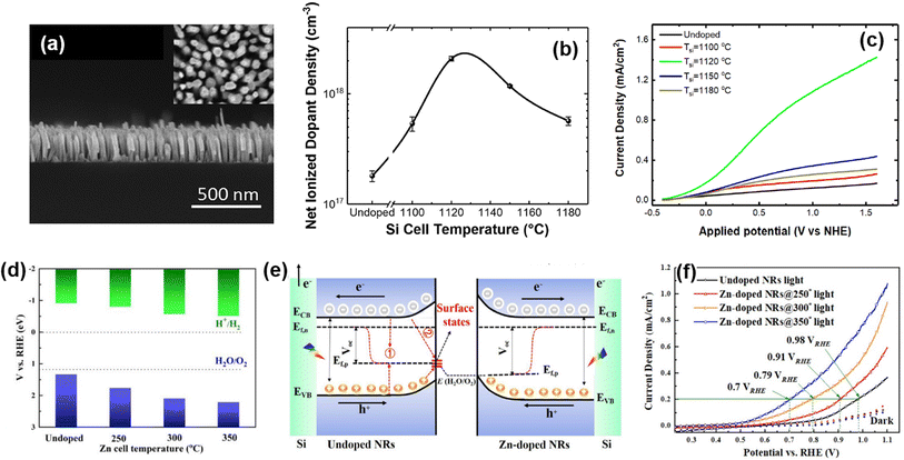 |
| | Fig. 3 (a) Cross-sectional view of the InGaN nanowire photoanode. (b) Net ionized dopant density of Si-doped InGaN nanowires with respect to Si cell temperature. (c) Linear sweep voltammetry (LSV) curves of Si-doped InGaN nanowire photoanodes. Reproduced from ref. 78. Copyright (2018) AIP Publishing. (d) Valance band and conduction band potentials of Zn-doped InGaN nanowires with respect to Zn cell temperature. (e) Band-bending diagram and charge carrier transport schematic of photoelectrochemical water oxidation for undoped and Zn-doped InGaN photoanodes. (f) LSV curves of Zn-doped InGaN nanowire photoanodes. Reproduced from ref. 79. Copyright (2020) Elsevier. | |
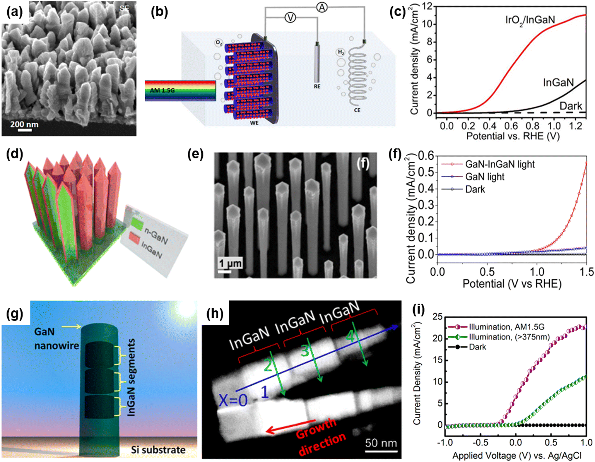
Alloying of In element to a GaN semiconductor can increase the charge carrier mobility and reduce the band gap energy to demonstrate broadband light absorption, thereby leading to an increase in photocurrent density for the photoelectrochemical water splitting reaction.101,102 Previously, an In-rich InGaN nanowire photoanode with a small band gap of 1.7 eV was grown on an n-type Si substrate by the MBE method.80 InGaN nanowires were vertically aligned on the Si substrate with an approximate diameter of ∼200 nm and height of ∼700 nm (Fig. 4a). To enhance the O2 evolution reaction, IrO2 nanoparticle cocatalysts were loaded on InGaN nanowires by a photodeposition process. The photoelectrochemical water oxidation performance of the InGaN nanowire photoanode was evaluated in an acidic electrolyte (0.5 M H2SO4) under an air mass 1.5 global (AM 1.5G) simulated 1 sun illumination in a three-electrode configuration (Fig. 4b). The pristine InGaN nanowires showed a low photocurrent density and a large overpotential due to the poor kinetics of the water oxidation reaction (Fig. 4c). However, after modification of InGaN with IrO2 cocatalysts, the activity of the photoelectrode greatly improved. Due to the unique 1D nanowire structure, a low energy band gap of 1.7 eV, and appropriate band edge positions to straddle the redox potentials of water splitting, together with effective coupling with IrOx cocatalysts, the InGaN nanowires resulted in a low onset potential of 0.1 VRHE, a high photocurrent density of 5.2 mA cm−2 at 0.6 VRHE, and a half-cell solar energy conversion efficiency up to 3.6%.
 |
| | Fig. 4 (a) Scanning electron microscopy (SEM) image of the InGaN nanowire. (b) Schematic illustration of the three-electrode cell for photoelectrochemical water oxidation. InGaN nanowire photoanode, Pt wire, and Ag/AgCl were used as the working, counter, and reference electrodes, respectively. (c) LSV curves of InGaN and IrOx/InGaN photoanodes in 0.5 M H2SO4 under light illumination. Reproduced from ref. 80. Copyright (2018) American Chemical Society. (d) Schematic illustration and (e) SEM image of GaN/InGaN core/shell nanorod arrays. (f) Current density vs. potential plots of GaN/InGaN core/shell nanorods photoanode and GaN nanorods in 0.01 M H2SO4 solution under 1 sun illumination using AM 1.5G filter. Reproduced from ref. 81. Copyright (2014) American Chemical Society. (g) Schematic illustration and (h) transmission electron microscopy (TEM) image of GaN nanowires with axially incorporated InGaN segments. (i) Anodic photocurrent density measured in 1 M HBr under simulated sunlight illumination with filters. Reproduced with permission from ref. 82. Copyright (2013) American Chemical Society. | |
In addition to the reduced band gap of InGaN nanowires, dual-band GaN/InGaN core/shell nanowires have been developed as visible-light-responsive photoelectrodes.103–106 For instance, GaN/InGaN core/shell nanowire arrays were fabricated by sequential growth of n-type GaN nanorods followed by an n-type InGaN coating using the MOCVD method (Fig. 4d).81 It is observed that GaN nanowires, with an average diameter of 900 nm and height of 14 μm, are covered by a 20 nm-thick InGaN layer (Fig. 4e). Compared to GaN nanowires, the GaN/InGaN nanowire photoanode showed 10-fold higher photocurrent density at an anodic potential of 1.35 VRHE (Fig. 4f). The photocurrent density enhancement was mainly attributed to the extended light absorption of the narrow band gap InGaN shells, which can utilize visible light and increase the number of photogenerated charge carriers. The InGaN segments can also be incorporated into 1D GaN nanowires along the axial direction by MBE growth (Fig. 4g).82 The high angle annular dark field (HAADF) image of InGaN/GaN nanowires illustrates the atomic number contrast between GaN (darker) and InGaN (brighter) regions and the presence of 3 segments of ∼70 nm long InGaN passivated by the GaN layer (Fig. 4h). This dual-band photoanode was first tested using a 375 nm long-pass filter, which prevents excitation of the GaN region. The photoanode revealed a photocurrent density of ∼11 mA cm−2 at 1 VAg/AgCl, indicating the excitation of charge carriers by InGaN segments under visible light. Notably, when an AM 1.5G filter was used, the photocurrent density was greatly enhanced to ∼23 mA cm−2 at 1 VAg/AgCl because of concurrent excitation of charge carriers in both InGaN and GaN regions. From these results, it was found that the strategy of integrating ultraviolet-light-absorbing GaN and visible-light-responsive InGaN into 1D nanostructures can have a synergistic effect on photoelectrochemical water splitting.
3.2. Heterostructure
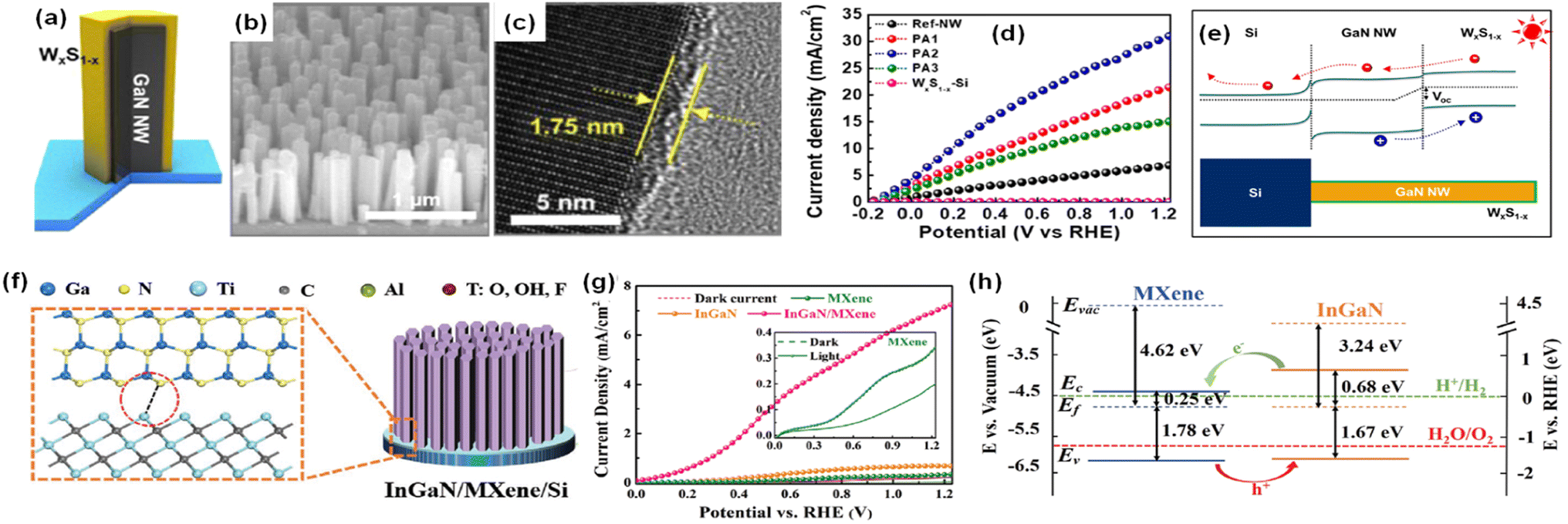
The design of a heterostructure by the combination of two or more semiconductor materials is a promising strategy for broadband light absorption, suppression of electron–hole recombination, and increased lifetime of photogenerated charge carriers. When two semiconductors with different work functions are in contact, the built-in electric field at the heterojunction interface can promote charge separation and increase the current density for photoelectrochemical water splitting. Thus, GaN and InGaN nanostructures combined with other semiconductors (ZnS,83 MoS2,88 C3N4,84 WxS1−x,85 MXene86) have been exploited in photoelectrochemical water splitting. For example, photoanodes, consisting of GaN nanowires coated with tungsten sulfide (WxS1−x), were fabricated by MBE growth of GaN and solvothermal synthesis of WxS1−x (Fig. 5a).85 The vertically grown GaN nanowires on an Si wafer had an average length of ∼443 nm and an average diameter of ∼35 nm (Fig. 5b). The average thicknesses of the WxS1−x layer could be varied from 0.79 to 3.23 nm depending on the synthesis conditions (Fig. 5c). The photoelectrochemical water oxidation performance was measured in 0.5 M H2SO4 under 1 sun illumination. The GaN–WxS1−x photoanode showed superior performance compared to GaN without WxS1−x. The photocurrent density was as high as 20.38 mA cm−2 at 0.6 VRHE and a maximum applied-bias photon-to-current efficiency (ABPE) of 13.76% was achieved (Fig. 5d). This greatly improved performance was attributed to the type-II band structure formed at the GaN/WxS1−x interface (Fig. 5e). In this photoanode configuration, the photogenerated holes efficiently transfer to the valence band of WxS1−x for the water oxidation reaction while the photogenerated electrons migrate to the conduction band of GaN nanowires, thereby leading to accelerated charge carrier separation and suppression of charge carrier recombination. In comparison to the deposition of semiconductors on 1D nitrides, direct growth of InGaN nanowires on MXene can also construct a heterostructure for photoelectrochemical water splitting.86 An MXene (Ti3C2Tx) film with a thickness of ∼50 nm was spin-coated on an n-type Si substrate. Then, InGaN nanorods were vertically grown on it by MBE (Fig. 5f). An MXene/InGaN nanorod photoanode revealed a very low onset potential and high photocurrent density of 7.27 mA cm−2 at 1.23 VRHE, which is over 10 times higher than that of an InGaN/Si photoanode (0.71 mA cm−2) (Fig. 5g). The low onset potential and high photocurrent density originate from the type-II band alignment at the InGaN/MXene interface where the photogenerated carriers can be efficiently separated, with electrons transferring from InGaN to MXene and holes transferring from MXene to InGaN for water oxidation (Fig. 5h). Overall, type-II heterostructures at the III-nitride and other semiconductor interfaces were found to enhance the photoelectrochemical water splitting performance by promoting the separation of photogenerated charge carriers.
 |
| | Fig. 5 (a) Schematic illustration, (b) SEM image, and (c) high-resolution TEM image of GaN nanowires covered with a WxS1−x layer. (d) Current density–potential curves of the GaN nanowires and GaN nanowires–WxS1−x photoanodes in 0.5 M H2SO4. (e) Energy band diagram of photoanode under light illumination. Reproduced with permission from ref. 85. Copyright (2020) American Chemical Society. (f) Schematic illustration of InGaN/MXene nanorods. (g) LSV curves of InGaN, MXene, and InGaN/MXene photoanodes. (h) Proposed band diagram of the InGaN/MXene heterojunction. Reproduced with permission from ref. 86. Copyright (2020) John Wiley and Sons. | |
3.3. Tunnel junction
Tunnel junction diodes, that connect a top cell with a large band gap and a bottom cell with a small band gap, have been extensively studied to address the current-matching issues for dual or triple absorber solar cells and photoelectrodes in III–V systems.107–110 Inspired by this strategy, III-nitride nanowire top cells grown on Si bottom cells have been developed for both photoanode and photocathode applications.90–92,111 A recent theoretical study on InGaN/Si double-junction photocathodes indicated that a high photocurrent density of up to ∼18 mA cm−2 can be demonstrated when an In0.46Ga0.54N top cell with a band gap of ∼1.8 eV is integrated on an Si bottom cell with a band gap of ∼1.1 eV (Fig. 6a).93 Hence, a p-type InGaN nanowire top cell was fabricated on a planar n+–p Si bottom cell and the top and bottom light absorbers are electronically connected through a p++-InGaN/n++-InGaN NW tunnel junction (Fig. 6b). In this structure, photogenerated electrons in the conduction band of the Si bottom cell migrate to the n+-InGaN segment, which then recombine with photogenerated holes in the valence band of the p++-InGaN segment in the tunnel junction (Fig. 6c). Meanwhile, the photogenerated electrons in the conduction band of the top p-InGaN nanowires laterally diffuse to Pt nanoparticle cocatalysts due to downward surface band bending and finally participate in the H2 evolution reaction.
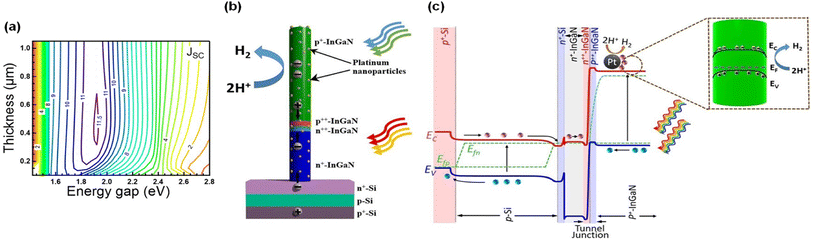 |
| | Fig. 6 (a) Theoretically calculated top p+-InGaN thickness and energy gap dependence of the short circuit current density of an InGaN/Si double-junction photocathode. (b) Schematic of Pt-decorated p+-InGaN/tunnel junction/n+-InGaN nanowire on an n+–p Si wafer. (c) Energy band diagram under light illumination, showing charge carrier generation in bottom Si and top p+-InGaN nanowire and electron migration to the lateral surface of p+-InGaN for proton reduction reaction. Reproduced with permission from ref. 93. Copyright (2021) AIP Publishing. | |
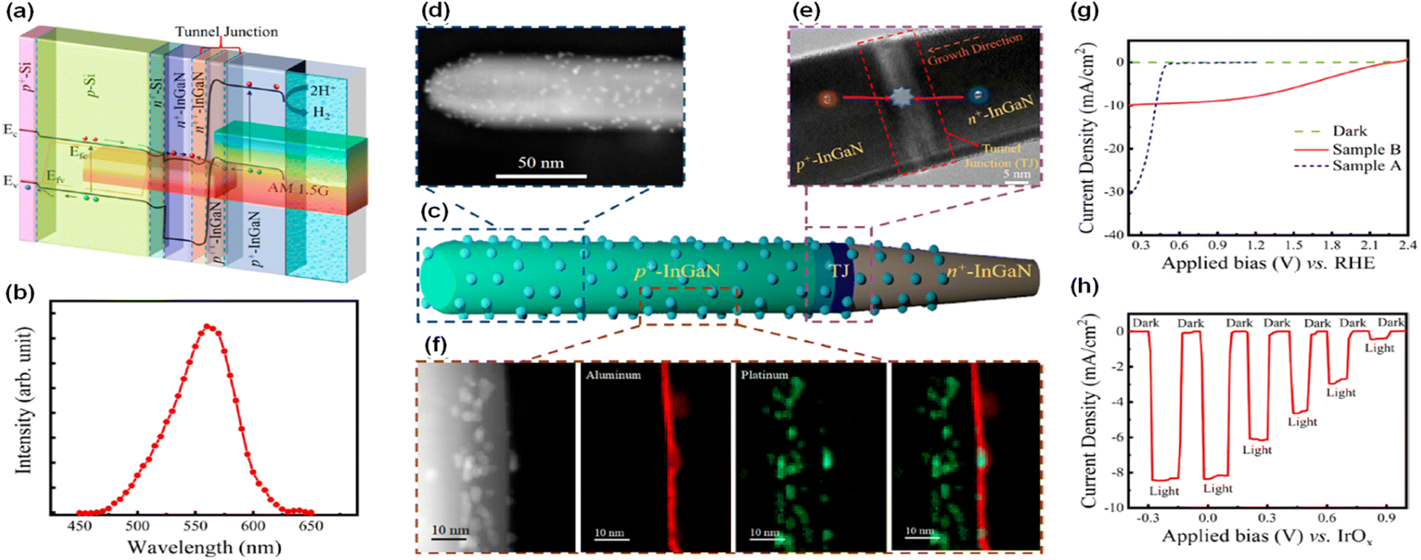
Even though the ideal band gap energy of an InGaN top cell on an Si bottom cell is ∼1.8 eV, it is extremely challenging to grow InGaN nanowires with high In composition (∼46%) because of unavoidable defect formation and phase separation. Therefore, an InGaN nanowire top cell with a band gap of 2.2 eV was integrated on an n+–p Si bottom cell through a nearly defect-free n+-InGaN/p+-InGaN NW tunnel junction for the photoelectrochemical H2 evolution reaction (Fig. 7a and b).94 Unlike a previous tunnel junction formed in an Si bottom cell,87 the tunnel junction was grown epitaxially in the InGaN nanowires (Fig. 7c–e). Since there is significantly reduced lattice mismatch, a high-crystal-quality tunnel junction can be formed with fewer defects and dislocations. Moreover, thin Al2O3 layer (1–2 nm) and Pt nanoparticle cocatalysts were deposited on the InGaN nanowires to passivate the surface defects and to prevent corrosion of the photocathodes, thereby leading to enhanced water splitting performance and stability (Fig. 7f). To elucidate the photoelectrochemical water splitting activity, an InGaN/Si double-junction photocathode (sample B) was compared with an n+-InGaN/Si single-junction photocathode without the tunnel junction (sample A) (Fig. 7g). Single-junction InGaN/Si showed an onset potential of ∼0.5 VRHE whereas double-junction InGaN/Si remarkably increased the onset potential to ∼2.3 VRHE. The saturation photocurrent density for the double-junction cell was ∼9 mA cm−2 which is smaller than that of the single-junction cell (∼30 mA cm−2) because the photocurrent density of the double-junction cell was limited by the top p+-InGaN nanowires (with a band gap of ∼2.2 eV) whereas the Si-based single-junction photocathode has a theoretical maximum photocurrent density of ∼44 mA cm−2. In addition, the InGaN/Si double-junction photocathode exhibited an onset potential of ∼0.7 V vs. an IrOx counter electrode in the 2-electrode configuration with a record-high solar-to-hydrogen (STH) efficiency of ∼10.3% under AM 1.5G 1 sun illumination (Fig. 7h). This double-junction photocathode provided sufficient built-in potential under solar light, leading to overall solar water splitting without additional electrical bias. Addressing the current-matching issues of top and bottom cells through a tunnel junction structure will further improve the photocurrent density while producing a built-in potential sufficient for overall water splitting.
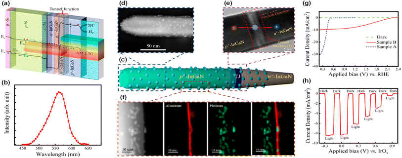 |
| | Fig. 7 (a) Band-diagram of the p+-InGaN/tunnel junction/n+–p Si photocathode.94 (b) Photoluminescence spectrum of p+-InGaN nanowires. (c) Schematic of a single nanowire with Pt cocatalysts and Al2O3 layer. (d) High angle annular dark field (HAADF) image of top p+-InGaN segment. (e) Bright-field image of tunnel junction region. The photogenerated holes from the p+-InGaN top cell and electrons from the bottom n+-InGaN recombine in the tunnel junction. (f) HAADF and elemental mapping showing Pt and Al2O3 on the nanowire sidewall. (g) Three-electrode linear scan voltammetry curves of InGaN/Si single-junction (sample A) and double-junction (sample B) photocathodes. (h) Two-electrode chopped photocurrent density curve of InGaN/Si double-junction in 0.5 M H2SO4 under AM 1.5G 1 sun illumination. Reproduced with permission from ref. 94. Copyright (2020) American Chemical Society. | |
3.4. Crystal orientation
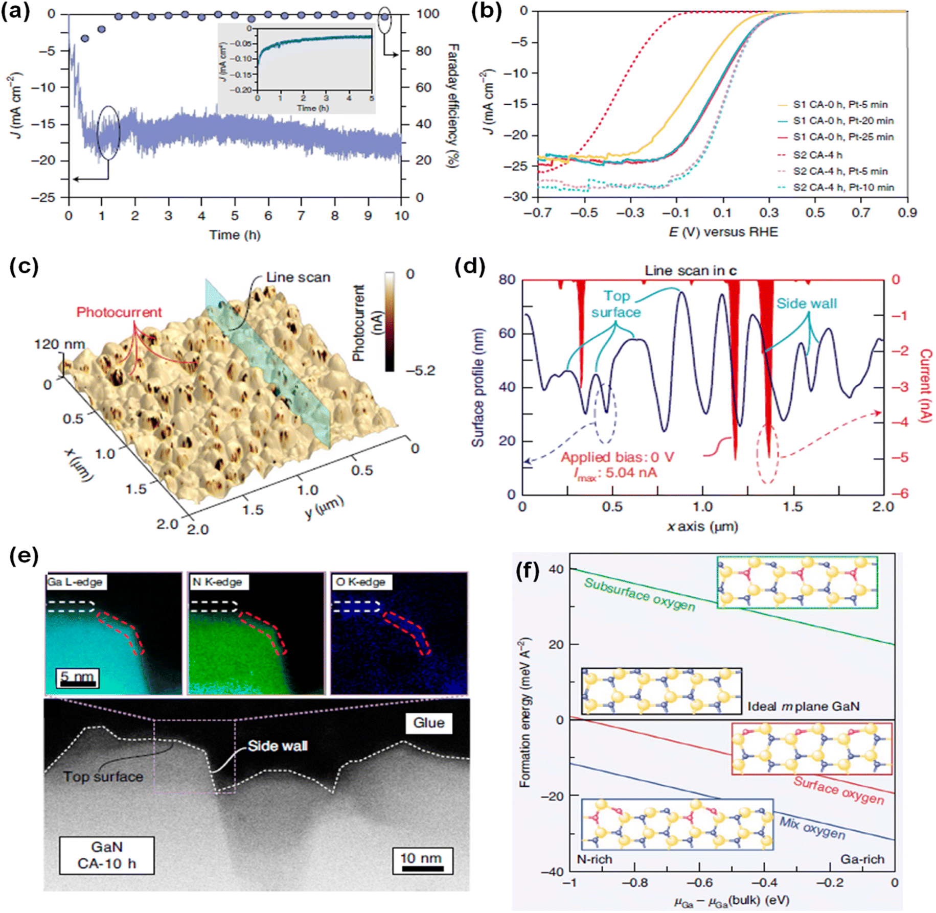
Due to distinct atomic arrangements on the different crystal facets of semiconductor materials, anisotropic physical and chemical properties have been demonstrated. Electrical conductivity, surface adsorption of molecules, band edge position, and direction of charge carrier diffusion in the photoelectrodes are highly dependent on the crystal orientation. In addition, each crystal facet has a different intrinsic reactivity dependent on the pH and applied potential. Hence, understanding crystal facet effects on photoelectrochemical water splitting activity and stability is an essential issue. Previously, specific crystal facets have been exposed to the surface of various photoelectrodes of TiO2,112 Fe2O3,113,114 WO3,115–117 BiVO4,118,119 Cu2O,120,121 Sb2Se3,122,123 and Ta3N5 (ref. 124 and 125) by selective nucleation, growth, or etching processes. Fine control over crystal orientation has exhibited an improvement in activity and stability for both photoelectrochemical H2 evolution and O2 evolution reactions. Although various studies have demonstrated efficient water splitting by optimization of the crystal structures of semiconductor materials, the effect of crystal facets of III-nitrides on water splitting performance has been largely unknown. Recently, GaN quasi-films grown on n+–p Si photocathodes showed a gradual self-improvement in H2 evolution activity during the initial several hours of chronoamperometry (CA) measurement in 0.5 M H2SO4 under 1 sun illumination at a cathodic bias of −0.6 VRHE (Fig. 8a).95 The linear sweep voltammetry (LSV) curves exhibited a positive shift in onset potential from −0.46 to −0.08 VRHE after 10 h of CA testing. Owing to the self-improving characteristic of GaN quasi-film, the loading amount of noble metal Pt cocatalyst can be greatly reduced. On the pristine GaN/Si photocathode, 20 min of Pt deposition was required to achieve an onset potential of ∼0.3 VRHE; meanwhile this onset potential can be demonstrated with 5 min of Pt deposition on a self-improved GaN/Si photoelectrode (Fig. 8b), indicating about a 4 times reduction in the amount of Pt cocatalysts. To elucidate the reason for the self-improvement, photoconductive atomic force microscopy measurements were carried out (Fig. 8c). Notably, pristine GaN and self-improved GaN showed similar surface morphology but a substantial difference in photocurrent profile. The photocurrent in self-improved GaN mainly flows through the side walls of the GaN grains, whereas the top surface barely contributes to the photocurrent (Fig. 8d). From the surface composition analysis of self-improved GaN through cross-sectional scanning transmission electron microscopy (STEM) measurement, a 1 nm-thin layer with Ga, N, and O was observed at the side wall and a relatively thick layer with Ga and O was formed on the top surface (Fig. 8e). Theoretical calculations suggested that partial substitution of nitrogen by oxygen during the reaction can stabilize the GaON phase on the outermost layer of the nonpolar side wall, whereas the GaO phase is more preferred on the polar top surface (Fig. 8f). These different atomic compositions, originating from the crystal facets and polarity of GaN, shifted the H2 evolution activity. The free energy of adsorption of hydrogen is smaller on GaON compared to the pristine GaN non-polar side wall, thereby resulting in the thermodynamically favorable production of H2.
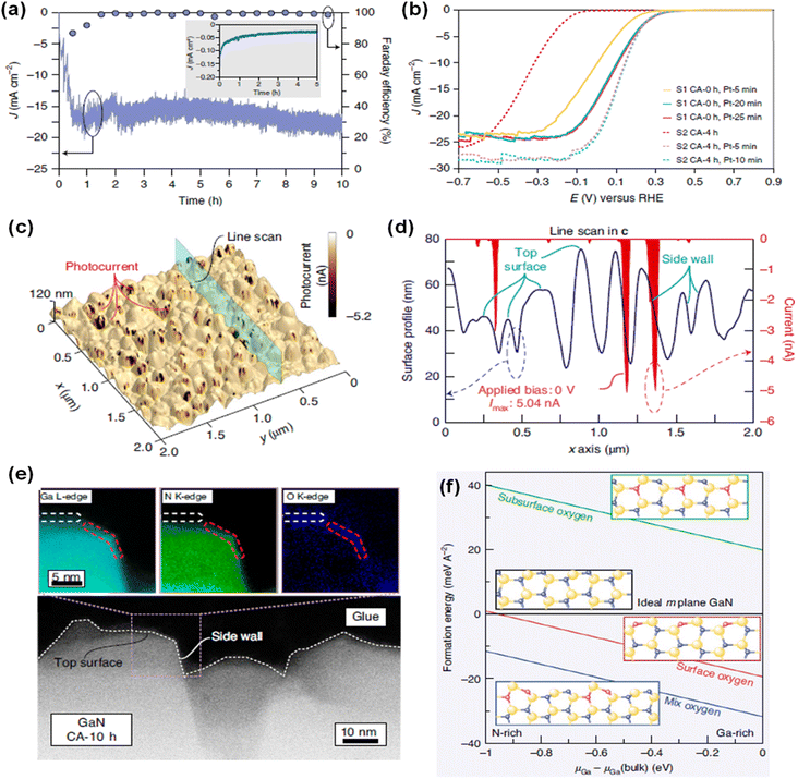 |
| | Fig. 8 (a) Current density and faradaic efficiency (FE) measurement of GaN quasi-film/n+–p Si photocathodes for 10 h under 1 sun illumination at −0.6 VRHE. Inset: Si control electrode. (b) LSV curves of pristine (CA-0 h) and 4 h tested (CA-4 h) GaN/Si photocathodes with different Pt deposition duration. (c) Topography of self-improved GaN quasi-film (CA-10 h) and (d) corresponding surface profile and photocurrent extracted from the line scan. (e) STEM image of CA-10 h surface with elemental mappings of Ga L-edge, N K-edge and O K-edge. (f) Calculated formation energy of nonpolar m-plane GaN surface with different oxygen configurations within the anion- and cation-rich limits. Reproduced with permission from ref. 95. Copyright (2021) Springer Nature Limited. | |
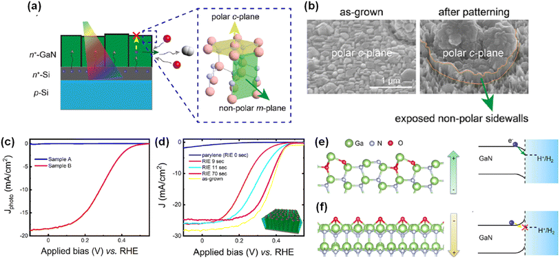
Inspired by the previous investigations, a detailed study on the effect of crystal facet and surface polarity of wurtzite III-nitride on photoelectrochemical activities was carried out. To identify the impact of crystal orientations with different polarities, GaN nanostructures were fabricated by both top-down and bottom-up methods, which allow the exposure of certain facets (polar top surface or nonpolar side wall) to the electrolyte (Fig. 9a).96 First, the GaN quasi-film (sample A) was grown on the n+–p Si wafer with preferential orientation along the c-plane direction (Fig. 9b). Then, patterning processes (photolithography and dry etching) were conducted to expose the nonpolar m-plane side walls (sample B). Even though a high photocurrent density (∼40 mA cm−2) is expected from an Si-based photocathode under 1 sun illumination, sample A showed negligible photocurrent density (Fig. 9c). In stark contrast, sample B exhibited a much better onset potential of ∼0.45 VRHE and saturation photocurrent density of ∼18 mA cm−2. Given that sample A and sample B are nearly identical except for the nonpolar surfaces exposed to the electrolyte, it is therefore found that the nonpolar surfaces of GaN are responsible for the H2 evolution reaction. Furthermore, GaN nanowire arrays were grown on the n+–p Si wafer. Then, their surface exposure to the electrolyte was controlled by the deposition of an insulating parylene passivation layer, followed by an etch-back process to reveal the top portions of the GaN nanowires. The as-grown GaN nanowire/Si photocathode with Pt cocatalysts exhibited an onset potential of 0.45 VRHE and a maximum photocurrent density of 28 mA cm−2 (Fig. 9d). Then, there was no photoresponse when the insulating passivation layer was deposited. However, after an initial etch-back process, the exposure of active nonpolar sidewalls of GaN nanowires greatly improved the performance. To understand the fundamental difference in the activity between polar and nonpolar planes, the role of oxygen was studied by density functional theory calculation. For the nonpolar surface, the most stable configuration was found to be gallium oxynitride formed by partial replacement of nitrogen by oxygen (Fig. 9e). On the other hand, for the polar surface, the most stable configuration was an oxygen-rich condition, which induces strong surface polarization and upward band bending at the surfaces (Fig. 9f). This observation describes the reason for the facilitated electron transport at the nonpolar plane and limited transport at the polar one. It is therefore evident that selective exposure of desired crystal facets of a III-nitride nanostructure can enhance charge carrier transport and photoelectrochemical water splitting activity.
 |
| | Fig. 9 (a) Schematic illustration of the H2 evolution reaction on the polar c-plane and nonpolar m-plane of wurtzite structure GaN. Photoexcited electrons preferentially migrate to the GaN nonpolar surfaces and reduce protons to H2. (b) SEM images of GaN quasi-film (sample A) and one that exposed the nonpolar sidewalls by a patterning process (sample B). (c) LSV curves of samples A and B in 0.5 M H2SO4 under AM 1.5G 1 sun illumination. (d) H2 evolution reaction of parylene-coated GaN nanowires. Longer durations of etch back exposed greater amounts of GaN nanowire nonpolar sidewalls. Schematic of configurations for surface polarization and surface energy band diagrams of (e) nonpolar m-plane with oxygen partial substitution and (f) polar c-plane with oxygen adsorption. Reproduced with permission from ref. 96. Copyright (2022) American Chemical Society. | |
3.5. Protective 1D nitrides for long-term stability
Many semiconductor photoelectrodes have been studied and developed for photoelectrochemical water splitting with a suitable decoration with cocatalysts or modification of nanostructures.126–130 However, most photoelectrodes with relatively high photocurrent density, such as Si and III–V semiconductors, suffer from a corrosion reaction in aqueous electrolytes because these materials have a very narrow window of stability based on their Pourbaix diagrams.131 To prevent cathodic or anodic corrosion during the water splitting reaction, the photocathode should have the material's self-reduction potential above the energy level of H2O/H2 and the photoanode should have the material's self-oxidation potential below the energy level of O2/H2O.132 Several metal oxides such as TiO2 (ref. 133) and Al2O3 (ref. 134) satisfy these thermodynamic requirements and, thus, have been used as protective layers for photoelectrodes. However, the charge carriers in metal oxides are known to have poor mobilities and short diffusion lengths. Moreover, an unsuitable band alignment at the metal oxide/semiconductor interface is a major obstacle to realizing efficient photoelectrodes. To mitigate these limitations, N-terminated GaN nanowire arrays have been fabricated as multifunctional protection structures for the underlying n+–p Si photoelectrode (Fig. 10a and b).97 GaN nanowires have several advantages of optical transparency, conduction band alignment between GaN and Si photocathode, and large surface area. GaN nanowires with a large band gap (∼3.4 eV) are transparent for visible and infrared light and allow an Si photoelectrode to absorb broadband solar light. Also, the conduction band edges of n-type GaN nanowire and n+-Si are approximately aligned, so the photogenerated electrons can efficiently transfer from Si to GaN without significant electrical resistance (Fig. 10c). Moreover, the large surface area of GaN nanowires can be loaded with Pt cocatalysts and behave as active sites for the H2 evolution reaction. As a result, Pt-decorated GaN/Si photocathodes showed a high saturated photocurrent density of ∼38 mA cm−2 with a promising onset potential of ∼0.5 VRHE in 0.5 M H2SO4 under 1 sun illumination (Fig. 10d). More notably, the Pt-decorated GaN/Si photocathodes showed excellent stability up to 3000 hours with relatively stable photocurrent densities of 37–38 mA cm−2 at 0 VRHE.135 Owing to the excellent physical and chemical stability of GaN nanowires,136 GaN nanostructures have also been deposited on a III–V GaInP2/GaAs/Ge triple-junction photocathode as a protective scheme (Fig. 10e).98 The GaN-protected triple-junction photocathode exhibited a saturated photocurrent density of 10.3 mA cm−2, an onset potential of 2.2 VRHE, and an ABPE of 12.6% (Fig. 10f). This photocathode can work continuously for 80 h without degradation (Fig. 10g), indicating the excellent stability, compatibility, and integrability of GaN nanostructures with high-performing semiconductors of Si and III–V photoelectrodes.
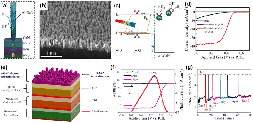 |
| | Fig. 10 (a) Schematic of GaN-nanowire-protected n+–p Si photocathode with Pt cocatalysts. (b) SEM image of GaN/Si photocathode. (c) Schematic of the energy band diagram of Pt-decorated GaN/Si photocathode under light illumination. (d) LSV curves measured under AM 1.5G 1 sun illumination in 0.5 M H2SO4. Reproduced with permission from ref. 97. Copyright (2018) American Chemical Society. (e) Schematic illustration of the GaInP2/GaAs/Ge triple-junction photocathode protected by GaN nanostructures. (f) Photoelectrochemical H2 evolution reaction performance and (g) long-term stability of GaN-protected triple-junction photoelectrode in 0.5 M H2SO4 under 1 sun illumination. Reproduced with permission from ref. 98. Copyright (2019) American Chemical Society. | |
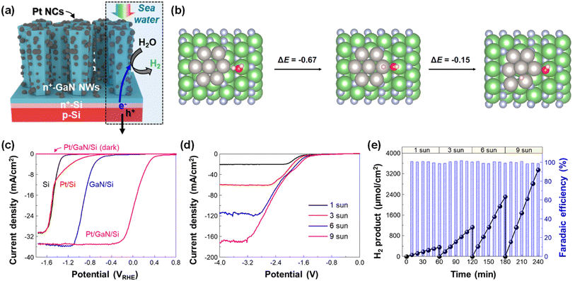
A green H2 fuel can be produced by the photoelectrolysis of seawater, which is the most abundant water source on earth. However, due to the sluggish water dissociation reaction, unfavorable precipitation of insoluble salts (e.g., Mg(OH)2 and Ca(OH)2), and most importantly, the poor stability of semiconductors in harsh reaction conditions, the application of photoelectrodes for seawater splitting has been limited. However, GaN nanowires, grown on an n+–p Si photoelectrode, have enabled efficient and stable seawater H2 evolution once Pt nanoclusters were decorated on the sidewalls of nanowires (Fig. 11a).99 Compared to water dissociation on Pt, the heterolytic cleavage of the water molecule at a Pt–Ga site was facilitated due to the asymmetric atomic environment (Fig. 11b). The overall energy change of water splitting at the Pt/GaN interface is −0.81 eV, indicating a spontaneous reaction without a thermodynamic energy barrier. Owing to the benefits from the synergistic interaction between GaN and Pt, an onset potential (0.16 VRHE) and a saturated photocurrent density (∼35 mA cm−2) of Pt/GaN/Si outperformed the other control devices (Fig. 11c). Moreover, the Pt/GaN/Si photocathode revealed a gradual increase in saturated photocurrent density, reaching ∼165 mA cm−2 at −3.2 V under concentrated solar light (9 sun) illumination in a 2-electrode configuration (Fig. 11d). Accordingly, the production rate of H2 gradually increased from 359 (under 1 sun illumination) to 3351 μmol cm−2 h−1 (under 9 sun illumination) while the faradaic efficiency was nearly 100% regardless of the light intensity (Fig. 11e). Therefore, a GaN-nanowire-protected Si photoelectrode is a promising platform for an efficient, stable, and energy-saving electrode for solar-assisted H2 generation by seawater splitting.
 |
| | Fig. 11 (a) Schematic illustration of the Pt/GaN/Si photocathode for seawater H2 evolution. (b) Optimized structures and calculated energy changes of water dissociation at the Pt–Ga site and subsequent H spillover to the Pt surface. All energy changes are in the units of eV. The white, red, blue, green, and grey spheres represent H, O, N, Ga, and Pt atoms, respectively. (c) LSV curves of Si, Pt/Si, GaN/Si, and Pt/GaN/Si measured with a 3-electrode configuration in 0.5 M NaCl solution under AM 1.5G 1 sun illumination or in the dark. (d) LSV curves of Pt/GaN/Si measured with 2-electrode configurations in 0.5 M NaCl under different light intensities. (e) Amount of H2 product and faradaic efficiency measured under light intensities of 1, 3, 6, and 9 suns at −3 V. Reproduced with permission from ref. 99. Copyright (2023) Springer Nature Limited. | |
4. Photocatalytic water splitting
In contrast to photoelectrochemical water splitting driven by solar light and electrical bias, photocatalytic water splitting, often referred to as type-I or type-II photoelectrochemical water splitting, is completely wireless and overall water splitting operates with only solar light as energy input. Moreover, in photocatalytic water splitting, pH-neutral pure water, or seawater can be readily utilized, in contrast to the strongly acidic or basic electrolytes commonly required for conventional photoelectrochemical water splitting. Therefore, photocatalytic water splitting is more amenable for the scaled-up production of solar hydrogen with reduced cost and enhanced stability. When the incident light illuminates the photocatalysts in water, the photocatalysts absorb photons with an energy larger than the band gap by exciting electrons in the conduction band and holes in the valence band. Then, the photoexcited electrons and holes separate and are transported to the surface active sites for the catalytic reactions. Because both water oxidation (H2O + 2h+ → ½O2 + 2H+) and reduction reactions (H2O + 2e− → H2 + OH−) occur at a photocatalyst, the semiconductor photocatalysts for overall water splitting should satisfy the requirements of band edge positions which must straddle the water reduction and oxidation potentials. Moreover, catalytic activity for stabilizing reaction intermediates is necessary to kinetically and thermodynamically enhance the productivity and selectivity for H2 and O2. Therefore, it is highly desirable to develop a photocatalyst material with a suitable band gap, band edge position, and surface active site for overall water splitting. Up to now, some metal oxides (i.e., TiO2 and SrTiO3) have demonstrated overall solar water splitting since they satisfy the requirements of band edge positions.137,138 However, those metal oxides possess relatively large band gaps due to the deeper-lying O 2p orbitals in the valence band edge. Consequently, they are photoresponsive only to ultraviolet light, which results in limited efficiency. In contrast, III-nitrides have a smaller band gap and less positive valence band edge positions, mainly consisting of N 2p orbitals. Therefore, 1D III-nitrides, such as InGaN nanowires, have shown great promise in photocatalytic water splitting (Table 3). Efficiency-enhancement strategies, such as band gap engineering, doping for surface band bending, and loading of cocatalysts, are introduced in the following sections.
Table 3 III-Nitride photocatalysts for photocatalytic overall water splitting
| Photocatalyst |
Cocatalyst |
Solution |
Light source |
Performance |
Ref. |
| p-InGaN/GaN NWs |
Rh/Cr2O3 |
Artificial seawater |
300 W Xe lamp |
STH conversion efficiency = 1.9% |
139
|
| InGaN/GaN NWs |
Rh/Cr2O3 and Co3O4 |
H2O |
300 W Xe lamp with AM 1.5G filter |
STH conversion efficiency = 2.7% |
140
|
| InGaN/GaN core/shell NWs |
Pt |
220 ml H2O with 50 ml CH3OH |
300 Xe lamp (1044 mW cm−2) |
H2 production rate = 253.3 μmol g−1 h−1 |
141
|
| InGaN/GaN NWs |
Rh/Cr2O3 |
H2O |
300 W Xe lamp |
H2 production rate = ∼92 mmol g−1 h−1 |
142
|
| Quadruple-band InGaN NWs |
Rh/Cr2O3 and Co3O4 |
H2O |
300 W Xe lamp with AM 1.5G filter |
STH conversion efficiency = ∼5.2% |
143
|
| Mg-doped GaN NWs |
Rh/Cr2O3 |
H2O |
300 W Xe lamp with >375 nm filter |
H2 + O2 production rate = ∼570 mmol g−1 h−1 |
144
|
| p-GaN NWs |
Rh/Cr2O3 |
H2O |
300 W Xe lamp |
H2 production rate = ∼4 mol g−1 h−1 |
145
|
| p-GaN/InGaN NWs |
Rh/Cr2O3 |
H2O |
300 W Xe lamp with AM 1.5G filter |
STH conversion efficiency = 1.8% |
146
|
| Mg-doped InGaN nanosheets |
Rh/Cr2O3 |
H2O |
300 W Xe lamp with AM 1.5G filter |
STH conversion efficiency = 3.3% |
147
|
| GaN nanorods |
Rh and CoOx |
H2O |
300 W Xe lamp |
Quantum efficiency = 6.9% |
148
|
| InGaN/GaN NWs |
Rh/Cr2O3/Co3O4 |
H2O at 70 °C |
300 W Xe lamp with AM 1.5G filter |
STH conversion efficiency = 9.2% |
149
|
4.1. Band gap engineering of 1D nitrides
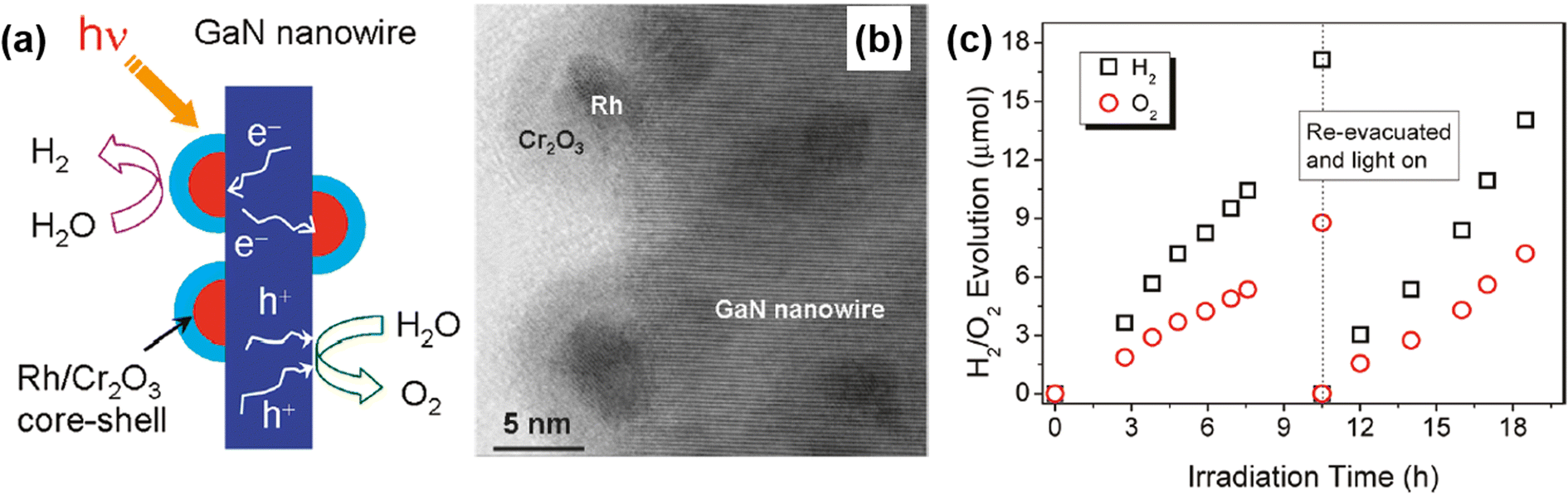
Unlike conventional photocatalysts in powder form, GaN nanowires, vertically grown on an Si wafer, have a single-crystalline structure with a small number of defects, resulting in efficient charge carrier transport to the surface active sites for photocatalytic water splitting. Hence, GaN nanowires decorated with Rh/Cr2O3 core/shell nanoparticles have been fabricated wherein the GaN is responsible for the O2 evolution reaction, the Rh core promotes the H2 evolution reaction, and the Cr2O3 shell prevents the backward reaction (Fig. 12a).150 From TEM characterization, it was found that GaN nanowires have a single crystalline structure and are uniformly coated by metallic Rh/Cr2O3 core/shell nanoparticles (Fig. 12b). Photocatalytic water splitting has been successfully carried out on 1D GaN nanowires with Rh/Cr2O3 cocatalysts in pure water under light irradiation. During ∼18 h of reaction, a stoichiometric ratio (2![[thin space (1/6-em)]](https://www.rsc.org/images/entities/char_2009.gif) :1) of H2 and O2 gases was steadily generated (Fig. 12c).
:1) of H2 and O2 gases was steadily generated (Fig. 12c).
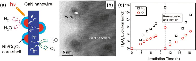 |
| | Fig. 12 (a) Schematic illustration of photocatalytic water splitting on GaN nanowire with Rh/Cr2O3 core/shell nanoparticle cocatalysts. (b) High-resolution TEM image of Rh/Cr2O3 cocatalysts on GaN nanowire. (c) H2 and O2 evolution under 300 W full arc xenon lamp irradiation for a duration of 18 h. Reproduced with permission from ref. 150. Copyright (2011) American Chemical Society. | |
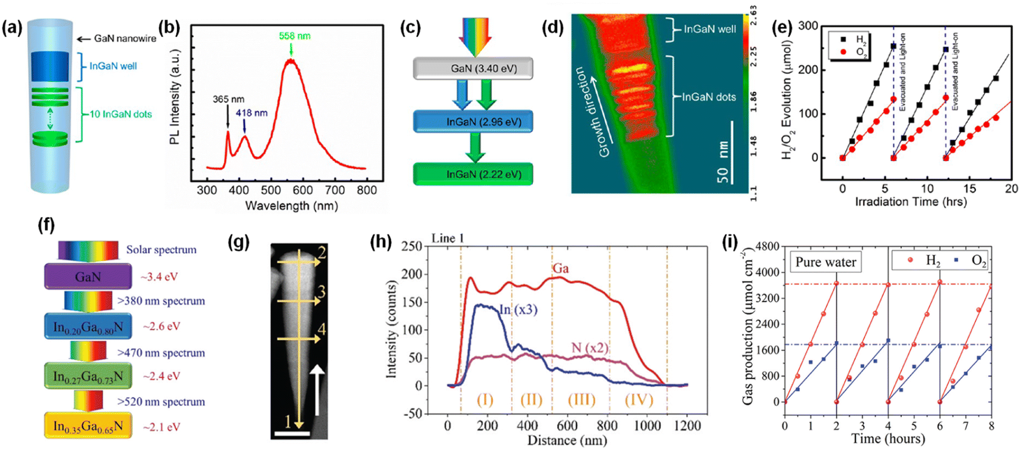
Although wafer-level photocatalytic water splitting has been demonstrated by GaN nanowires, a very small portion of solar light (mostly ultraviolet light) can be absorbed due to the large band gap (∼3.4 eV). The band gap of InxGa1−xN can ideally be controlled from 3.4 eV to 0.65 eV and, thus, the visible-to-near infrared solar spectrum can be used for photocatalytic overall water splitting. However, it is extremely challenging to grow the InGaN nanowires with a narrow band gap due to phase-separation issues and an increase in the number of detrimental defects. Moreover, the decrease in band gap energy of III-nitride semiconductors inevitably shifts the valence band edge potential in a more negative direction and/or the conduction band edge positions in a more positive direction, thereby resulting in a decrease in the redox ability. To mitigate these issues, multi-band InGaN/GaN nanowire photocatalysts have been developed to enhance the STH efficiency.139–141 For example, sequential deposition of GaN (band gap = 3.4 eV), InGaN quantum dots (2.22 eV), and InGaN wells (2.96 eV) reduced the lattice mismatch at the hetero-interfaces and enabled the epitaxial growth of nanowire photocatalysts with a multi-band structure (Fig. 13a–c).142 The HAADF image of InGaN/GaN nanowire exhibited an obvious atomic number contrast and the presence of 10 InGaN/GaN quantum dots located along the axial direction of the nanowire (Fig. 13d). InGaN/GaN nanowires with Rh/Cr2O3 cocatalysts showed overall pure water splitting under light illumination. The high production rates of H2 (∼683 μmol) and O2 (∼373 μmol) were concurrently demonstrated during 18 h of reaction (Fig. 13e), indicating that the broader band light absorption induced more photogenerated charge carriers and promoted the photocatalytic water splitting reactions compared to GaN nanowires. Furthermore, quadruple-band InxGaN1−x nanowires consisting of continuous In0.35Ga0.65N (2.10 eV), In0.27Ga0.73N (2.40 eV), In0.20Ga0.80N (2.60 eV), and GaN (3.40 eV) segments have been successfully grown on an Si wafer by MBE (Fig. 13f).143 The InxGaN1−x nanowires showed an inversely tapering morphology (Fig. 13g) and 4 distinct regions with different In content (Fig. 13h). Besides, gradient doping of Mg along the lateral dimension of the nanowires induces an internal electric field, which facilitates electron–hole separation (the effect of Mg doping in InGaN nanowires will be described in Section 4.2). These advantageous optoelectronic properties of quadruple-band InxGaN1−x nanowires greatly enhanced the photocatalytic overall water splitting and achieved a high STH (Fig. 13i).
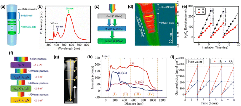 |
| | Fig. 13 (a) Schematic and (b) photoluminescence spectra of InGaN/GaN nanowires. (c) Band gap energy of each segment. (d) HAADF image in pseudocolor display of InGaN/GaN nanowire, showing the atomic number contrast between InGaN (red) and GaN (green) segments. (e) Overall pure water splitting on Rh/Cr2O3-decorated InGaN/GaN nanowires under full arc (>300 nm) 300 W xenon lamp irradiation. Reproduced with permission from ref. 142. Copyright (2013) American Chemical Society. (f) Schematic light absorption sequence and (g) TEM image of quadruple-band InGaN nanowire with various indium compositions. (h) Energy-dispersive X-ray spectroscopy line scanning showing the variation in Ga, In, and N elements along the axial direction. (i) Photocatalytic H2 and O2 gas evolution as a function of time. Reproduced with permission from ref. 143. Copyright (2019) Royal Society of Chemistry. | |
4.2. Doping of 1D nitrides
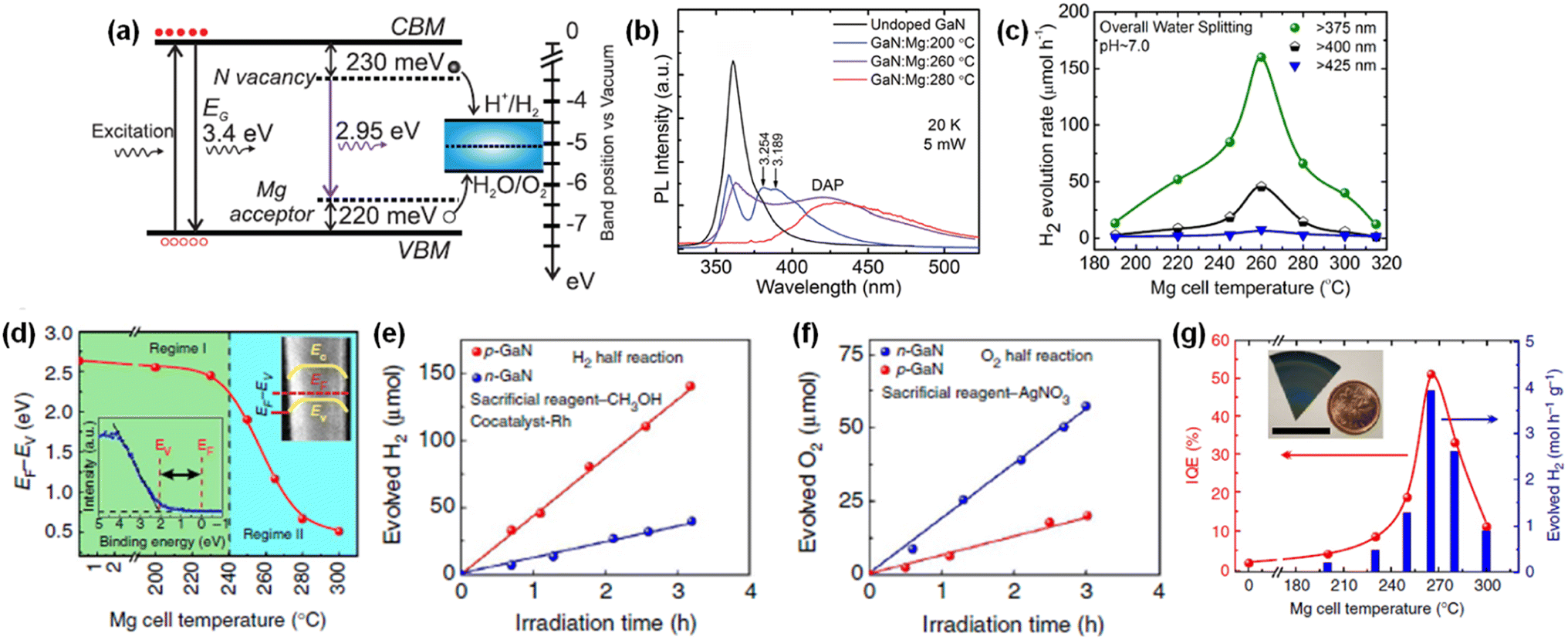
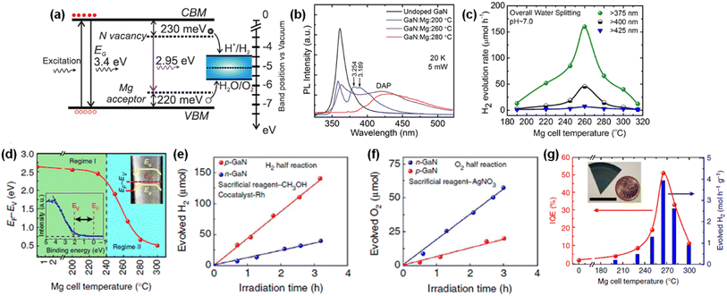
Intrinsic III-nitrides can be changed to p-type semiconductors with Mg doping. Hence, the effect of Mg dopant in GaN nanowires on light response, charge carrier transport, and photocatalytic activity of overall water splitting has been investigated. To vary the amount of Mg dopant, the Mg effusion cell temperature was changed from 190 to 315 °C during the MBE growth of GaN nanowires.144 Low-temperature (20 K) photoluminescent spectra of pristine GaN showed a single peak at 3.435 eV, corresponding to a donor-bound exciton. With a small amount of Mg doping (200 °C), GaN:Mg nanowires showed two additional peaks at 3.254 and 3.189 eV, which are attributed to the conduction band to Mg-related acceptor level (Fig. 14a). With a further increase in the amount of Mg dopant (260 °C), a new broad photoluminescence peak at 2.95 eV appeared due to the donor–acceptor-pair transition between the N-vacancy deep donor states and shallow Mg acceptor states. With the intra-gap defect states which straddle the redox potential of water (Fig. 14b), GaN:Mg nanowires enable broadband light absorption and enhance the performance of overall water splitting (Fig. 14c). However, it should be noted that further incorporation of Mg dopant in GaN nanowires (>260 °C) drastically degrades the water splitting activity because of poor crystal quality and undesirable non-radiative recombination of photogenerated carriers. Hence, optimized doping of III-nitride photocatalysts can broaden the light-responsive wavelength and, accordingly, increase the productivity of overall water splitting under solar light irradiation.
 |
| | Fig. 14 (a) Schematic energy band diagram of Mg-doped GaN nanowires. (b) Low-temperature photoluminescence spectra of GaN:Mg and undoped GaN nanowires. (c) H2 evolution rate from photocatalytic water splitting from the GaN:Mg samples under 300 W xenon lamp. Reproduced with permission from ref. 144. Copyright (2015) AIP Publishing. (d) Plot of EF − EV for different GaN:Mg nanowires. Regimes I and II indicate n-type and p-type surfaces, respectively. (e) H2 and (f) O2 evolution reactions from n- and p-type GaN nanowires in the presence of sacrificial reagents. (g) H2 evolution rate and internal quantum efficiency for different GaN:Mg nanowires in overall pure water splitting. Reproduced with permission from ref. 145. Copyright (2014) Nature Publishing Group, a division of Macmillan Publishers Limited. | |
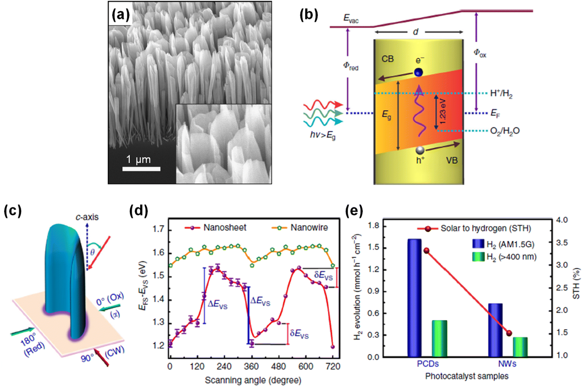
Moreover, previous studies revealed that n-type and p-type doping of GaN surfaces results in upward and downward band bending, respectively, once water is adsorbed on the surface, which can promote the separation of photogenerated electron–hole pairs at the semiconductor/water interface.151,152 Since GaN nanowires have a weakly n-type nature with the Fermi level located higher than the redox potential of water, the fine-tuning of the p-type dopant in GaN nanowires can reduce the downward band bending and provide an opportunity to realize the balanced surface band structure for efficient photocatalytic water splitting reactions.145 The amount of p-type Mg dopant was in situ controlled during the MBE growth of GaN nanowires by varying the Mg effusion cell temperature (TMg). Then, the near-surface band structure of GaN:Mg nanowire was investigated by measuring the Fermi level position (EF) relative to the valence band maximum (EV) by X-ray photoelectron spectroscopy (Fig. 14d). The EF − EV was 2.63 eV for undoped GaN, indicating an n-type semiconductor property. However, as TMg increased over 240 °C, the near-surface EF − EV dramatically decreased due to the increased free hole concentration in GaN nanowires from p-type doping. To evaluate the effect of surface band bending on photocatalytic water splitting, H2 and O2 half-reactions were measured in the presence of sacrificial reagents in the electrolytes. The H2 production rate of p-type GaN nanowires was much higher than that of n-type GaN nanowires owing to downward band bending (Fig. 14e). On the other hand, the O2 production rate of n-type GaN nanowires was significantly enhanced due to efficient hole transport by upward band bending (Fig. 14f). Hence, to demonstrate efficient overall water splitting, it is desirable to construct a nearly flat band profile at the GaN/water interface. Consequently, the optimum incorporation of p-type Mg dopants in GaN nanowires decreased the downward band bending, which led to an improvement in STH efficiency by more than two orders of magnitude compared to n-type GaN nanowires (Fig. 14g). Moreover, it is also found that this p-type doping strategy is applicable to visible-light-responsive InGaN nanowires.146 A gradual decrease in near-surface EF − EV (gradual change from n-type to p-type) was observed with an increasing amount of Mg dopant in InGaN nanowires. With optimized InGaN:Mg nanowires, a high yield of H2 evolution (∼0.8 mol h−1 g−1) and STH efficiency (1.8%) were achieved with stoichiometric O2 evolution under visible light wavelength.
In addition to surface band bending, a built-in potential in bulk regions of III-nitride is highly desirable for efficient charge carrier separation. Previously, two-dimensional p-type InGaN nanosheets with gradient Mg doping were developed as photocatalysts for overall water splitting (Fig. 15a).147 During the growth, Mg dopants impinged preferentially on one side, thereby leading to gradient doping of Mg along the lateral dimension of the nanosheets. This configuration induced a strong internal electric field that separated the electrons in the conduction band and holes in the valence band toward opposite surfaces with significantly suppressed non-radiative recombination (Fig. 15b). From the near-surface band structures of p-InGaN nanowires and nanosheets (Fig. 15c), a sharp change in EF − EV (∼300 mV) vs. scanning angle on p-InGaN nanosheets was observed. This confirmed that there is a strong internal electric field within the nanosheet due to the Mg dopant gradient from one side to the other (Fig. 15d). In contrast, p-InGaN nanowires showed nearly constant EF − EV regardless of scanning angle because of the symmetric morphology of the nanowires. As a result, p-InGaN nanosheets realized remarkable enhancement in activity for the photocatalytic water splitting reaction over p-InGaN nanowires and achieved an impressive STH efficiency of ∼3.3% (Fig. 15e).
 |
| | Fig. 15 (a) SEM image of Mg-doped p-InGaN nanosheets vertically grown on an Si substrate. (b) Energy-band diagram of p-InGaN nanosheet with radial thickness “d” showing the built-in electric field (band-bending) that separates the electrons and holes towards opposite surfaces. (c) Schematic illustration of probing the surface valence band spectra using X-ray photoelectron spectroscopy. (d) EFS − EVS for Mg-doped InGaN nanosheets and nanowire arrays as a function of radial scanning angle (α). (e) H2 evolution rate in overall water splitting for photochemical diodes (nanosheets) and nanowires under different excitation conditions. All the photocatalysts were decorated with Rh/Cr2O3 cocatalysts. Reproduced with permission from ref. 147. Copyright (2018) Springer Nature Limited. | |
4.3. Polarity of 1D nitrides
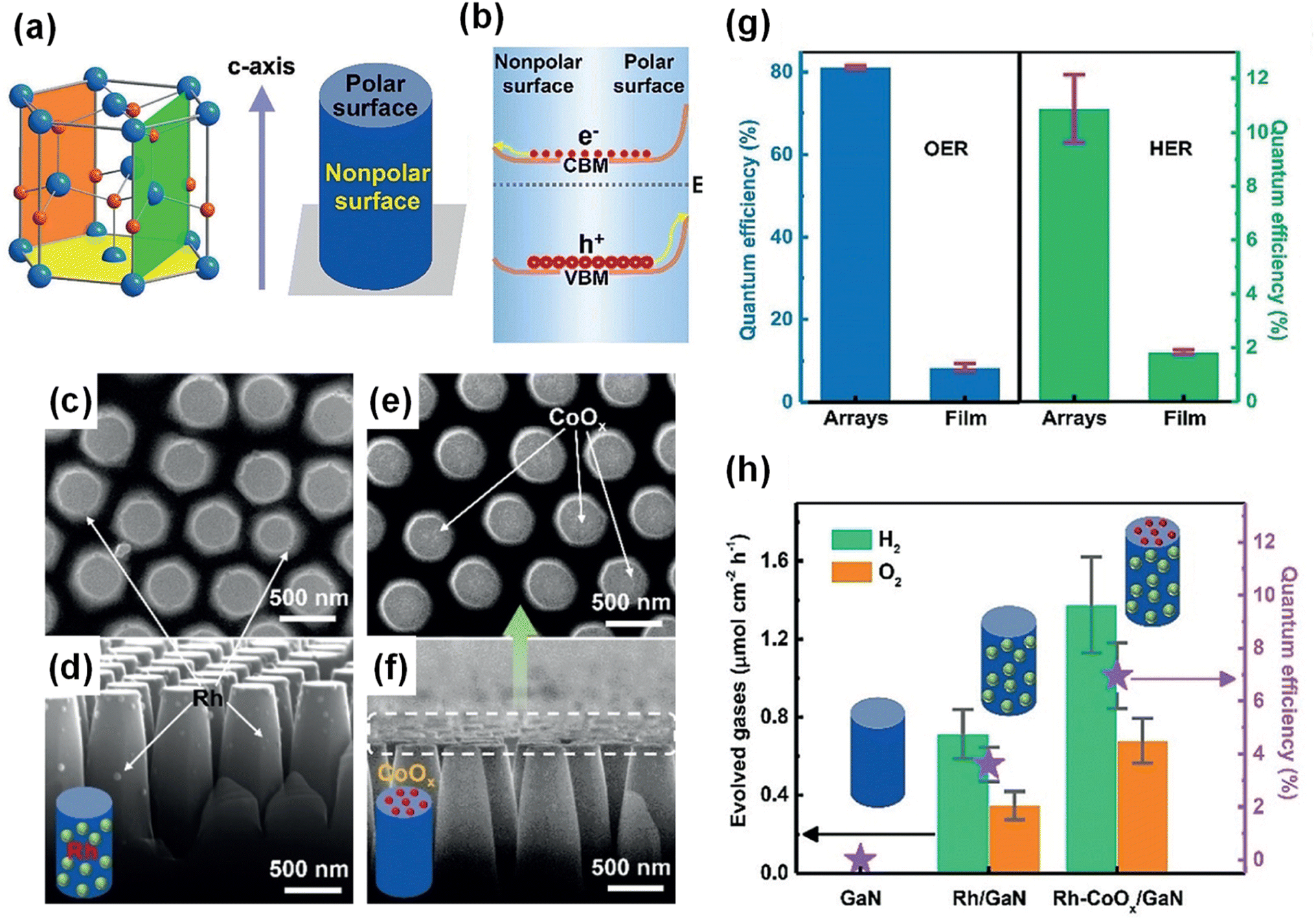
The ionic bonds in a unit cell of crystalline III-nitride semiconductors can induce electric dipole moments, thereby resulting in positive charges on one surface and negative charges on the other, which then produces a substantial electric field directed from the positively poled regions to those negatively poled. This electric field can redistribute the photogenerated charge carriers in III-nitrides and have a great influence on photocatalytic water splitting reactions. It is well known that GaN is generally grown along the polar c-axis [0001] direction on a c-plane sapphire substrate, resulting in the exposure of the polar surface (Ga-polar or N-polar).153 In order to expose the buried nonpolar plane (parallel to c-axis) to the surface, n-type GaN film was etched into nanorod arrays (Fig. 16a).148 Thus, the GaN nanorod arrays have a top polar surface (Ga-polar) and a nonpolar side surface. Based on surface band bending analysis, it was found that the upward band bending of the polar surface is more pronounced than that of the nonpolar surface, which leads to spatial separation of photogenerated electrons to the nonpolar surface and holes to the polar surface (Fig. 16b). The charge separation characteristics of GaN nanorod arrays can be investigated through the photochemical deposition method, in which reduced metals and oxidized metal oxides are coated on the electron-rich sites and hole-rich sites, respectively. After the photodeposition of Au, Rh, and Ag through the reduction of metal ions, metal nanoparticles were selectively coated on the nonpolar surface (side surface) (Fig. 16c and d). In stark contrast, MnOx and CoOx, deposited through an oxidation reaction, were found on the polar surface (top surface) (Fig. 16e and f). Owing to the polarity-driven electron–hole separation to redox active sites, the GaN nanorod arrays exhibited much higher photocatalytic water splitting activity compared to GaN film (Fig. 16g). In addition, the selective deposition of CoOx and Rh cocatalysts on the respective top and side surfaces greatly enhanced the overall water splitting (Fig. 16h).
 |
| | Fig. 16 (a) Schematic representation of polar c-plane (yellow), nonpolar a-plane (green), and m-plane (orange) of a GaN crystal, as well as the surface polarity of GaN nanorod arrays.148 (b) Schematic representation of different band bending on polar and nonpolar surfaces and the resulting spatial charge separation. (c–f) SEM images of GaN nanorod arrays with (c and d) Rh and (e and f) CoOx cocatalysts. (g) Photocatalytic O2 and H2 evolution reaction on GaN nanorod arrays and film coated with Rh and CoOx cocatalysts. (h) Photocatalytic overall water splitting on GaN nanorod arrays without and with cocatalysts Rh and CoOx. Reproduced with permission from ref. 148. Copyright (2020) John Wiley and Sons. | |
4.4. Temperature-dependent solar water splitting
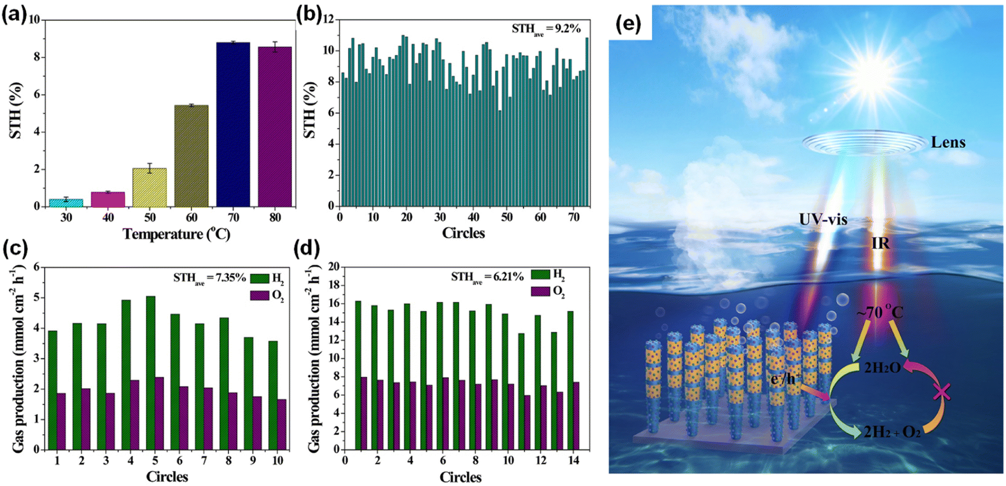
During the photocatalytic overall water splitting, the forward reaction of H2 and O2 evolution (2H2O → 2H2 + O2) often competes with the backward reaction of H2–O2 recombination (2H2O ← 2H2 + O2). Even though some cocatalysts (i.e., Rh/Cr2O3 core/shell nanoparticles150) loaded on InGaN/GaN nanowires have promoted the forward reaction, the catalytic activity of a III-nitride photocatalyst at higher temperature has remained unknown. Therefore, photocatalytic water splitting was conducted at different temperatures from 30 °C to 80 °C by illuminating with concentrated simulated solar light (3800 mW cm−2).149 InGaN/GaN nanowires decorated with Rh/Cr2O3/Co3O4 cocatalysts exhibited a dramatic increase in STH efficiency with increasing temperature (Fig. 17a). The maximum STH efficiency of 8.8% was achieved at 70 °C. Theoretical calculation elucidated that most steps of water splitting reactions were exothermal except for the water desorption step in H2–O2 recombination, meaning that H2–O2 recombination is suppressed as the temperature increases. However, further increasing the temperature to 80 °C did not improve the STH efficiency because the enhanced diffusivity of H2 and O2 promoted mass transfer in water and accelerated H2–O2 recombination. The Rh/Cr2O3/Co3O4–InGaN/GaN photocatalyst showed a world-record STH efficiency of 9.2% and promising stability for 74 hours at the optimized temperature of 70 °C (Fig. 17b). Moreover, the photocatalysts, evaluated in tap water (Fig. 17c) and seawater, exhibited very high STH efficiencies of 7.4% and 6.6%, respectively, showing high potential for practical use. In principle, it is possible to reduce material costs when more solar energy can be utilized in a given irradiated area. Hence, a 4 cm × 4 cm photocatalyst wafer was immersed in water and exposed to concentrated natural solar light (∼16070 mW cm−2). This outdoor test showed that the chamber could be self-heated and maintained at a high temperature (75 ± 3 °C). As a result, the highest reported STH efficiency of 6.2% was achieved under natural solar light (Fig. 17d). This work is the first demonstration that a III-nitride photocatalyst not only utilizes ultraviolet-visible light for photoexcitation of charge carriers but also benefits from the thermal energy generated by infrared light (Fig. 17e).
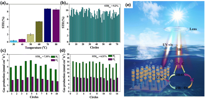 |
| | Fig. 17 (a) Temperature-dependent STH efficiency of Rh/Cr2O3/Co3O4–InGaN/GaN nanowires (a concentrated light of 3800 mW cm−2 with AM 1.5G filter was used). (b) Stability in the self-heated photocatalytic overall water splitting system. Each circle = 1 hour. (c) Measured STH in tapwater under 3800 mW cm−2. Each circle = 1 hour. (d) STH of 4 cm × 4 cm photocatalyst under concentrated natural solar light (∼16070 mW cm−2). Each circle = 10 min. (e) Synergetic effect mechanism of promoting forward H2–O2 evolution and inhibiting reverse H2–O2 recombination in photocatalytic overall water splitting. Reproduced with permission from ref. 149. Copyright (2023) Springer Nature Limited. | |
5. Photoelectrochemical CO2 reduction
Photosynthesis is widely known as the biochemical reaction which fixes CO2 gas in the atmosphere into carbon-based species under solar light. This solar-driven biochemical process can be mimicked by semiconductors where the photogenerated charge carriers under solar light are transported to the surface, interact with CO2 molecules, and catalytically convert the activated CO2 molecules into other carbon products through deoxygenation and/or hydrogenation processes. Compared to the electrocatalytic CO2 reduction reaction, whose efficiency is determined by the catalytic activity of the electrocatalyst, light absorption, electron–hole separation, charge carrier transport, and band alignment must be additionally considered to design an artificial photosynthetic device. Although these challenging requirements have limited the number of semiconductors, careful selection of semiconductors and catalyst materials, and optimization of device structures have realized the CO2 reduction reaction.154–167 Recently, 1D nanostructured semiconductor nanowires, nanorods, and nanofibers have surpassed the CO2 reduction reactivity of planar structures due to enhanced light absorption, shortened charge carrier pathways, and exposure of active sites.168–175 In particular, the emerging 1D III-nitrides have shown great promise for efficient and stable conversion of CO2 gas into target products.
The photoelectrochemical CO2 reduction reaction can convert the greenhouse CO2 gas to value-added chemicals by simultaneously illumination with solar light and application of an electrical bias to semiconductor photocathodes. Despite the light absorption, charge carrier excitation, separation, and transport processes of the photoelectrochemical CO2 reduction reaction being very similar to those of the photoelectrochemical hydrogen evolution reaction, the CO2 reduction reaction is much more complex due to the many possible reaction pathways coming from different reaction intermediates. Depending on the binding modes of intermediates on the surface of the electrodes, the selectivity and productivity of target chemicals can be changed. For example, an intermediate produced by CO2 accepting an electron and a proton could be *COOH with C attached to the surface or *OCHO with O attached to the electrode. The different intermediates play a vital role in determining the final products (i.e., CO, HCOOH, CH4, C2H4, C2H5OH, etc.). III-Nitride semiconductors, however, do not possess good catalytic activity toward the CO2 reduction reaction, probably due to unfavorable CO2 adsorption in comparison to the proton reduction reaction which can be operated with a pristine GaN photocathode. This bottleneck has been addressed by adapting appropriate cocatalysts on III-nitride photocathodes for the selective production of target chemicals, such as carbon monoxide (CO), formic acid (HCOOH), and methane (CH4) (Table 4).
Table 4 III-Nitride photocathodes for photoelectrochemical CO2 reduction reaction
| Photocathode |
Cocatalyst |
Applied potential |
CO2 feedstock |
Main products |
Faradaic efficiency |
Current density |
Ref. |
| p-GaN film |
Au |
−1.8 VRHE |
Pure CO2 |
CO |
CO: 83% |
∼2 μA cm−2 |
176
|
| GaN nanowires/n+–p Si |
ZnO–Cu |
0.17 VRHE |
Pure CO2 |
CO |
CO: 70% |
<1 mA cm−2 (8 sun illumination) |
177
|
| GaN nanowires/n+–p Si |
TiO2–Pt |
0.27 VRHE |
Pure CO2 |
CO, H2 |
CO: ∼33%, H2: ∼66% |
∼15 mA cm−2 (8 sun illumination) |
178
|
| GaN nanowires/n+–p Si |
AuPt0.2 |
0.17 VRHE |
Pure CO2 |
CO, H2 |
CO: ∼33%, H2: ∼66% |
∼9 mA cm−2 |
179
|
| GaN nanowires/n+–p Si |
Au |
0.17 VRHE |
Pure CO2 |
CO, H2 |
CO: ∼55%, H2: ∼45% |
∼3 mA cm−2 |
180
|
| GaN nanowires/n+–p Si |
AgBr |
−0.4 VRHE |
Pure CO2 |
CO |
CO: 82%, H2: 17% |
13.8 mA cm−2 |
181
|
| GaN nanowires/n+–p Si |
Sn |
−0.53 VRHE |
Pure CO2 |
HCOOH |
HCOOH: 76.9% |
∼11 mA cm−2 |
182
|
| GaN nanowires/n+–p Si |
Bi |
−0.6 VRHE |
Pure CO2 |
HCOOH |
HCOOH: 95% |
∼10.3 mA cm−2 |
183
|
| GaN nanowires/n+–p Si |
Cu |
−1.5 VAg/AgCl |
Pure CO2 |
CH4 |
CH4: 18% |
∼30 mA cm−2 |
184
|
| GaN nanowires/n+–p Si |
Cu–Fe |
−1.2 VRHE |
Pure CO2 |
CH4 |
CH4: 51% |
38.3 mA cm−2 |
185
|
| GaN nanowires/n+–p Si |
CuS |
−1.0 VRHE |
CO2 with H2S |
HCOOH |
HCOOH: 70.2% |
7.07 mA cm−2 |
186
|
| GaN nanowires/n+–p Si |
Au |
0.17 VRHE |
CO2 with NOx, SOx, or O2 |
CO |
CO: ∼90% |
∼4 mA cm−2 |
187
|
5.1. CO production
Among the various products (e.g., CO, HCOOH, CH4, C2H4, CH3OH, and C2H5OH), that can be produced from CO2 reduction reactions, CO and HCOOH are the kinetically most favorable products due to the simple two-proton-coupled electron transfer process. In addition, the reaction of synthetic gas (CO and H2) can produce methanol and other important chemicals and fuels through the well-established Fischer–Tropsch method.188,189 Therefore, III-nitride semiconductors decorated with cocatalysts have been investigated for the photoelectrochemical reduction of CO2 gas to CO. The feasibility of an Au cocatalyst has been evaluated on a p-GaN film for CO2 conversion to CO.176 The p-GaN photocathode coated with Au nanoparticles showed an onset potential of about 0.4 VRHE, a cathodic photocurrent density of 1.8 μA cm−2 at −0.8 VRHE (Fig. 18a), and CO-to-H2 ratio of 5:1 at −1.8 VRHE (Fig. 18b), whereas the bare p-GaN photocathode exhibited no photoresponse under visible-light illumination. The drastic improvement in photoresponse can be explained by a greater collection efficiency of hot holes from plasmonic Au nanoparticles to the valence band of p-GaN. Compared to previous n-type semiconductors with good hot electron collection properties (Fig. 18c), the Au/p-GaN interface can establish a more suitable Schottky barrier for hot hole collection (Fig. 18d). Thus, remaining hot electrons in Au nanoparticles can participate in the CO2 reduction reaction. This implies the positive effect of downward band bending at the metal cocatalyst/semiconductor photocathode not only for the electron–hole separation but also for the efficient photoelectrochemical CO2 reduction reaction.
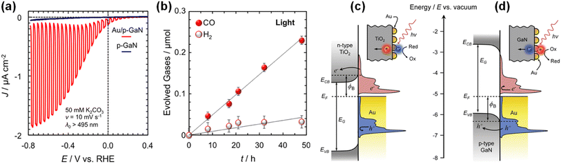 |
| | Fig. 18 (a) LSV of plasmonic Au/p-GaN and bare p-GaN photocathodes at 10 mV s−1 under periodic (0.5 Hz) visible-light irradiation (λ > 495 nm) at a power of 600 mW cm−2. (b) CO and H2 evolution using an Au/p-GaN photocathode. (c) Energy band diagrams of Au in physical contact with an n-type semiconductor (e.g., TiO2) and (d) with p-type semiconductor (e.g., p-GaN) for hot electron and hot hole collection, respectively. Reproduced with permission from ref. 176. Copyright (2018) American Chemical Society. | |
As was mentioned in the previous section, the large band gap of GaN (∼3.4 eV) cannot afford visible light absorption, which limits the photocurrent density. In addition, planar GaN has a small specific surface area capable of holding a cocatalyst. To solve these problems, 1D GaN nanowires were vertically grown on the n+–p Si photocathode. Since the GaN nanowires have ∼10 times larger surface area than the planar structure, a large number of cocatalysts can be loaded and the catalytic activity for the CO2 reduction reaction can be greatly improved. In this configuration, the photoexcited charge carriers are mainly generated in the n+–p Si photocathode and the photogenerated electrons migrate to cocatalysts through n+-GaN nanowires. In order to concurrently facilitate electron transport and promote catalytic performance, Cu–ZnO cocatalysts have been deposited on GaN nanowires (Fig. 19a).177 The conduction band of ZnO is located below that of GaN, so the photogenerated electrons can migrate to surface Cu catalysts without a significant energy barrier (Fig. 19b). As a result, the ZnO–Cu/GaN/n+–p Si photocathode attained a high photocurrent density (∼10 mA cm−2) (Fig. 19c) and demonstrated a higher faradaic efficiency (FE) of CO (20%) at −0.33 VRHE compared to control samples with ZnO (14.3%) and Cu (1.7%) cocatalysts (Fig. 19d). Inspired by this metal-oxide/metal cocatalyst loaded on GaN nanowires for CO production, a TiO2–Pt cocatalyst has been evaluated on a GaN nanowires/n+–p Si photocathode and revealed a positive onset potential of ∼0.5 VRHE and ∼2 times higher photocurrent density compared to photocathodes with TiO2 or Pt cocatalysts (Fig. 19e).178 The FE of CO was low on pristine GaN/n+–p Si and with individual TiO2 and Pt cocatalysts (1.7%, 5.6%, and 2%, respectively), while it increased remarkably to 32% by employing TiO2–Pt binary cocatalysts, indicating the synergetic interaction between Pt and TiO2 for the CO2 reduction reaction (Fig. 19f). Furthermore, two metal-oxide/metal cocatalysts of ZnO–Pt and TiO2–Pd exhibited higher CO selectivity compared to metallic Pt and Pd (Fig. 19g). To understand the mechanistic role of the metal-oxide/metal interface for CO2 reduction to CO, density functional theory calculations were carried out (Fig. 19h). It was found that CO2 is not activated on a Pt cocatalyst but strongly interacts with the TiO2–Pt binary cocatalyst. The carbon atom of the CO2 molecule at the interface binds to the metallic atom (Pt) and one of oxygen atoms attaches to the Ti atom of TiO2. This interaction greatly stabilizes the CO2 adsorption and facilitates the formation of *CO via an *COOH intermediate, thereby resulting in a thermodynamically downhill process.
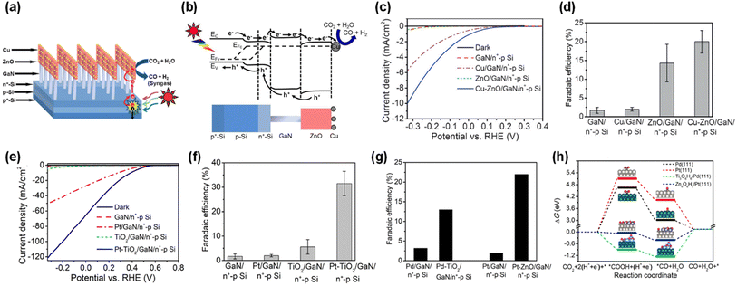 |
| | Fig. 19 (a) Schematic and (b) energy band diagram of Cu–ZnO/GaN/n+–p Si photocathode under light illumination. (c) LSV curves and (d) FE of CO at −0.33 VRHE. Reproduced with permission from ref. 177. Copyright (2016) John Wiley and Sons. (e) LSV curves and (f) FE of CO for pristine GaN/Si and GaN/Si with Pt, TiO2, and Pt–TiO2 cocatalysts. (g) FE of CO at 0.27 VRHE for GaN/Si photocathodes with Pd, Pd–TiO2, Pt, and Pt–ZnO cocatalysts. (h) Calculated free energy diagrams for CO2 reduction to CO. Green, Pt: gray, Ti: blue, Zn: purple, O: red, C: brown and H: white. Reproduced with permission from ref. 178. Copyright (2018) American Chemical Society. | |
Despite the GaN nanowires/n+–p Si photocathode being able to increase CO selectivity by metal-oxide/metal cocatalysts, the true reactivity and role of GaN nanowires are largely unknown since the GaN surface covered by cocatalysts was not exposed to the electrolyte during the CO2 reduction reaction. Therefore, Au and Pt cocatalysts have been directly coated on GaN nanowires without a metal oxide passivation layer.179 Au nanoparticles were prepared on top of GaN nanowires by an electron-beam evaporation method followed by thermal annealing, and Pt nanoparticles were coated on the sidewalls of GaN nanowires by a photodeposition method (Fig. 20a and b). These spatially separated Au and Pt cocatalysts preferentially convert CO2-to-CO and H+-to-H2, respectively. Control of the product distribution (i.e., CO/H2 syngas ratio) can be realized by tuning the composition ratio of Au and Pt cocatalysts. As the ratio of Pt increased in AuPtx/GaN/n+–p Si, the FE of H2 gradually increased from ∼10% to ∼99% with a decreased FE for CO from ∼90% to nearly zero (Fig. 20c). By adjusting the cocatalyst composition on GaN nanowires, the syngas ratio of CO/H2 could be varied over a wide range from 1:99 to 10:1. Furthermore, the size effect of Au nanoparticles was studied for syngas production on a GaN/n+–p Si photocathode.180 A gradual increase in CO selectivity with decreasing H2 selectivity was observed with increasing particle size at 0.17 VRHE under solar irradiation (Fig. 20d). As the size of Au nanoparticles with an icosahedral structure increases, the ratio of facet sites increases and, at the same time, the portion of edge and corner sites decreases (Fig. 20e). From theoretical calculation, it was found that H2 evolution, the major competitive reaction, becomes much easier on the corner and edge sites than on facet sites (Fig. 20f). Therefore, the facet sites of large Au nanoparticles (16 nm) are responsible for the reduction reaction of CO2 into CO while dominant corner and edge sites of small Au nanoparticles (3 nm) are active for the H2 evolution reaction.
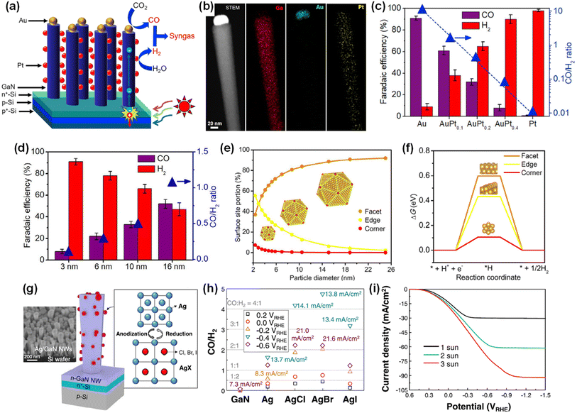 |
| | Fig. 20 (a) Schematic of an AuPtx/GaN/n+–p Si photocathode under light illumination. (b) STEM-energy dispersive X-ray spectroscopy elemental mapping images. (c) FE of CO and H2 for AuPtx/GaN/n+–p Si photocathodes at 0.17 VRHE. Reproduced with permission from ref. 179. Copyright (2020) Elsevier. (d) Size dependence of photoelectrochemical CO2 reduction performance on Au nanoparticles at 0.17 VRHE. (e) Portion of surface sites on icosahedron Au nanoparticles vs. particle size. (f) Free energy diagram of proton reduction into H2 on facet, edge, and corner sites of Au nanoparticles. Reproduced with permission from ref. 180. Copyright (2022) Elsevier. (g) SEM image of Ag-decorated GaN nanowires and schematic fabrication processes of Ag halide cocatalysts. (h) Plots of the CO/H2 ratio for the photocathodes at different potentials from 0.2 to −0.6 VRHE. (i) LSV curves of AgBr/GaN/Si under concentrated solar light. Reproduced with permission from ref. 181. Copyright (2022) American Chemical Society. | |
In addition to crystal facet engineering, Ag and Ag halide cocatalysts have been modified using phase engineering on vertically grown GaN nanowires by a photoelectrochemical anodization method (Fig. 20g).181 Compared to the metallic Ag nanoparticles, AgCl and AgBr cocatalysts greatly improved the selectivity and productivity of CO compared to H2 (Fig. 20h). This indicates that fine control over the material composition of cocatalysts can alter the surface electronic properties and consequent catalytic activity for CO2 conversion. Moreover, GaN/n+–p Si photocathodes with AgBr cocatalysts showed a very high photocurrent density of ∼92 mA cm−2 at −1.0 VRHE under concentrated solar light (3 sun illumination) (Fig. 20i). Stable and continuous production of CO could be achieved for 12 h without losing catalytic activity.
5.2. HCOOH production
HCOOH is an energy-dense liquid fuel and a building block for modern chemistry. There have been extensive developments of metallic electrocatalysts, such as Pb, Hg, Cd, Pd, In, Sn, and Bi, for the selective conversion of CO2 into HCOOH in aqueous electrolytes.190–198 However, the cost of expensive metals (Pd and In) and the toxicity of heavy metals (Pb, Cd, Hg) are a hindrance to practical application. Hence, the environmentally benign metals Sn, Bi, and their compounds have been spotlighted.199–201 Previously, Sn nanoparticles were electrochemically deposited on GaN nanowires grown on n+–p Si for the photoelectrochemical CO2 reduction reaction to HCOOH (Fig. 21a).182 Compared to the negligible productivity (2.1 μmol cm−2 h−1) of HCOOH on the Sn/n+–p Si photocathode, the productivity (201 μmol cm−2 h−1) of Sn/GaN/n+–p Si was nearly two orders of magnitude higher (Fig. 21b). This indicates that 1D GaN nanowires not only function as a support for cocatalysts and an electron-migration channel but also participate in the CO2 reduction reaction. Density functional theoretical calculation elucidated that the CO2 molecule can be easily activated and readily dissociated into *CO via a covalent-like Ga–C bond and an ionic-like Sn–O bond over the Sn/GaN interface, respectively (Fig. 21c). Then, the reduction of a key intermediate of CO* to HCOOH follows an energetically favorable reaction pathway (Fig. 21d). It is of scientific interest to find that III-nitride integrated with cocatalyst results in beneficial synergy for CO2 activation and HCOOH production.
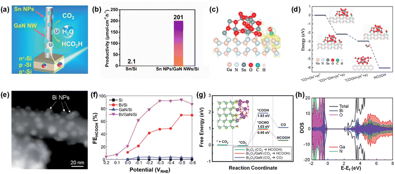 |
| | Fig. 21 (a) Schematic of Sn nanoparticles/GaN nanowires/n+–p Si for photoelectrochemical CO2 reduction with H2O to HCOOH. (b) Productivity of HCOOH for Sn/Si and Sn/GaN/Si photocathodes. (c) Calculated differential charge density for *CO/Sn13O26/GaN. (d) Potential energy diagram of reducing CO2 to HCOOH at the Sn/GaN interface. Reproduced with permission from ref. 182. Copyright (2019) Royal Society of Chemistry. (e) HAADF STEM image of Bi nanoparticles/GaN nanowires. (f) FE of HCOOH for photocathodes. (g) Free-energy profiles for the CO2 reduction reaction to HCOOH and CO on Bi2O3 and Bi2O3/GaN. (h) Density of states of Bi2O3/GaN near the band gap. Reproduced with permission from ref. 183. Copyright (2022) Royal Society of Chemistry. | |
Metallic Bi can also play a role as an efficient cocatalyst for photoelectrochemical CO2-to-HCOOH conversion when it is integrated with a GaN/n+–p Si electrode.183 A simple one-step thermal evaporation of Bi cocatalysts on GaN nanowires induces uniformly distributed Bi/Bi2O3 nanoparticles (Fig. 21e). Noticeably, a Bi/GaN/Si photocathode showed a high FE of HCOOH > 95% at −0.3 VRHE whereas Bi/Si exhibited a low FE of HCOOH < 70% and a relatively small photocurrent density (Fig. 21f). The reasons for the high HCOOH selectivity were the lowered catalytic energy barrier originating from Bi2O3/GaN interfacial interaction (Fig. 21g) and efficient transport of photogenerated electrons from GaN to Bi2O3 due to conduction band alignment (Fig. 21h). This work showed a promising insight that a strong electronic interaction between cocatalyst and 1D III-nitride can shift the intrinsic catalytic activity and realize a new class of material for an efficient photoelectrochemical CO2 reduction reaction.
5.3. CH4 production
Electrochemical production of CH4 from CO2 faces challenges of sluggish kinetics and a competitive proton reduction reaction. Cu and its alloys are known to be state-of-the-art catalysts for converting CO2 to high-order products.202–204 Therefore, Cu nanoparticles have been decorated on GaN/n+–p Si for a photoelectrochemical CO2 reduction reaction to CH4.184 A small amount of CO was produced on pristine GaN nanowires and CH4 product was not detected by gas chromatographic measurement (Fig. 22a and b). In stark contrast, Cu cocatalysts on both GaN/n+–p Si and n+–p Si boosted the photocurrent density, positively shifted the onset potential, and increased the FE of CH4. More interestingly, the Cu cocatalysts loaded on GaN nanowires showed higher selectivity for CH4 (∼18%) than those on the Si photoelectrode (∼4%). To enhance the catalytic activity of photocathode, binary Cu–Fe cocatalysts have been developed on GaN/n+–p Si.185 From theoretical calculation, it was found that a Cu and Fe binary catalyst activates the inert CO2 molecule by bending the O–C–O angle from 180° to 126.05° and by elongating the C–O bond length (Fig. 22c and d). The thermodynamic energy barrier of the potential-determining step (i.e., *CO → *CHO) for CO2-to-CH4 conversion was reduced from 0.85 to 0.51 eV by incorporating Fe into Cu catalysts (Fig. 22e). The binary Cu–Fe showed better onset potential and higher photocurrent density compared to single Cu or Fe catalysts on GaN/n+–p Si. Moreover, FE of CH4 increased to 51%, which is superior to that of the Cu cocatalyst (∼19%) under identical measurement conditions (Fig. 22f). Rational design of cocatalysts and 1D III-nitrides with high catalytic activity for CO2-to-CH4 conversion is found to be essential for the efficient and selective photoelectrochemical synthesis of high-order products such as CH4.
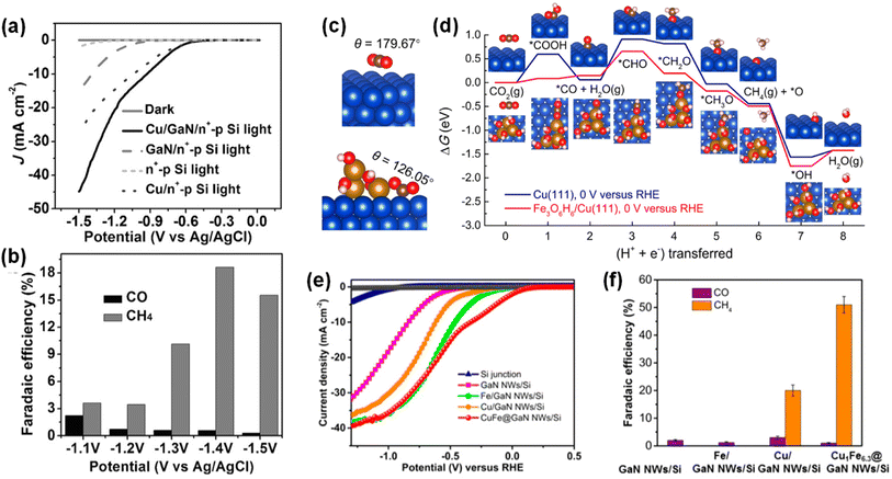 |
| | Fig. 22 (a) LSV curves of n+–p Si and GaN nanowires/n+–p Si photocathodes with/without Cu cocatalysts. (b) FE of CO and CH4 produced from a Cu/GaN/Si photocathode. Reproduced with permission from ref. 184. Copyright (2016) John Wiley and Sons. (c) The optimized configurations of the CO2 molecule on Cu(111) and Fe3O6H6/Cu(111). Blue, orange, red, brown, and white spheres represent Cu, Fe, O, C, and H atoms, respectively. (d) Free-energy diagrams for CO2 reduction to CH4 on Cu and the Fe3O6H6/Cu interface. (e) LSV curves and (f) FE of CO and CH4 for GaN/Si photocathodes with Fe, Cu, and Cu–Fe cocatalysts. Reproduced with permission from ref. 185. Copyright (2020) National Academy of Science. | |
5.4. Flue gas CO2 reduction
Until now, most studies have focused on the development of photocathodes using a pure CO2 feedstock. However, for practical application, their compatibility with flue-gas CO2 should be considered. Flue-gas CO2 usually contains many impurities, such as H2, CO, NOx, SOx, and H2S compounds. Hence, it is of great interest to convert impurity-containing flue-gas CO2 into value-added chemicals without a costly purification process.205–207 Recently, a photocathode consisting of a CuS cocatalyst loaded on GaN nanowires/n+–p Si has been presented as a promising architecture for the efficient and stable conversion of an H2S-containing CO2 mixture gas to HCOOH.186 Cu nanoparticles were firstly deposited on GaN nanowires and then spontaneously transformed to CuS nanoparticles by H2S impurity dissolved in the electrolyte during the CO2 reduction reaction (Fig. 23a). After the photoelectrochemical CO2 reduction reaction, CuS compounds can be clearly seen on GaN nanowires (Fig. 23b). In order to evaluate Cu and CuS cocatalysts on photocathodes, a photoelectrochemical CO2 reduction reaction was conducted in CO2- or CO2 + H2S-purged electrolyte, respectively. Cu and CuS cocatalysts integrated with GaN nanowires grown on n+–p Si (GaN/Si) showed a substantial improvement in onset potential and photocurrent density compared to those of Cu/Si and CuS/Si (Fig. 23c). An increase in the selectivity for HCOOH was observed from ∼21% to ∼32% when Cu cocatalysts were converted to CuS on an n+–p Si photocathode at −1.0 VRHE (Fig. 23d). Impressively, the transformation of Cu to CuS nanoparticles on GaN nanowires greatly increased the FE of HCOOH from ∼20% to ∼70% under the same conditions. This demonstrates that H2S impurity mixed in the CO2 gas can enhance, rather than degrade, the performance of the photoelectrochemical CO2 reduction reaction. CuS/GaN/Si revealed constant photocurrent densities of ∼4.5 and ∼7.8 mA cm−2 and consistently produced high FE of ∼60% and ∼70% at −0.8 and −1.0 VRHE, respectively (Fig. 23e). This outstanding stability is likely due to the chemical stability of the unique N-rich GaN surface which can withstand oxidation or sulfurization by impurities in the flue-gas CO2.
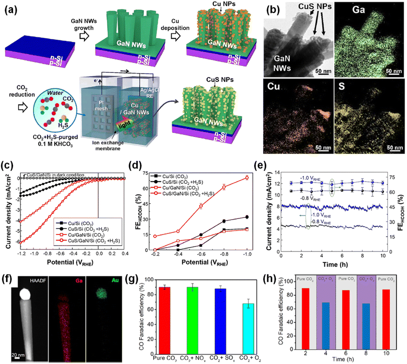 |
| | Fig. 23 (a) Schematic fabrication process of CuS/GaN/Si by MBE growth of GaN nanowires on n+–p Si, electron-beam deposition of Cu nanoparticles, and spontaneous transformation of Cu to CuS cocatalysts. (b) TEM analysis of CuS nanoparticles on GaN nanowires. (c) LSV curves and (d) FE of HCOOH for photocathodes measured in CO2- or CO2 + H2S-purged electrolytes. (e) Stability of CuS/GaN/Si photocathode at −0.8 and −1.0 VRHE. Reproduced with permission from ref. 186. Copyright (2021) American Chemical Society. (f) Structural characterization of Au/GaN/Si. (g) FE of CO at 0.17 VRHE measured with impurities of NOx, SOx, and O2 mixed in CO2 gas. (h) Time-dependent CO FE with or without O2 impurity gas. Reproduced with permission from ref. 187. Copyright (2022) Elsevier. | |
The influence of various impurities (0.1% NOx, 1% SOx, and 5% O2) on the photoelectrochemical CO2 reduction performance was also tested using Au nanoparticles deposited on top of GaN nanowire arrays on n+–p Si (Fig. 23f).187 The effects of NOx and SOx on CO2 reduction reaction to CO were negligible (Fig. 23g). In contrast, the presence of O2 impurity decreased the FE of CO from 90% to 68% due to the more favorable O2 reduction reaction. Although the O2 impurity led to a temporary decrease in the FE of CO, it could be fully recovered when a pure CO2 feedstock was purged, indicating the negligible long-term impact of O2 on the photocathodes (Fig. 23h). From these results, it was found that 1D GaN nanowires are chemically stable against impurity gases mixed in flue-gas CO2 and function as a good photocathode platform for the CO2 reduction reaction.
6. Photocatalytic CO2 reduction reaction
1D III-nitride photocathodes can drive a half-reaction of the CO2 reduction reaction and the other oxidation reaction takes a place at the counter electrode. In contrast, both CO2 reduction and oxidation reactions occur at the surface of 1D III-nitride photocatalysts during photocatalytic CO2 conversion reaction. During photocatalytic CO2 reduction, intermediates on the surface can be reduced or simultaneously oxidized to produce a variety of chemical products that are rarely obtainable with cathodic half-reactions alone. In addition to the requirements of conventional photocatalysts (i.e., band edge positions, charge carrier separation, and transportation), the kinetic balance between the CO2 reduction and oxidation reactions is mandatory for the selective production of target chemicals. Because GaN nanowires fulfill the requirements of band edge positions (the conduction band positions are higher than the reductive potential of CO2 reduction and the valence band is located lower than the water oxidation reaction) (Fig. 24a), 1D III-nitrides are desirable platforms for the photocatalytic CO2 reduction reaction, as demonstrated by several experiments (Table 5). In addition, GaN nanowires can readily activate the adsorbed CO2 by bending the linear O–C–O bonds, thereby resulting in the effective CO2 reduction reaction toward CO even without a cocatalyst (Fig. 24b).208 However, pristine GaN nanowires cannot efficiently produce CH4 since the CO2-to-CH4 conversion is kinetically and thermodynamically unfavorable because of the high reaction barrier and complicated 8H+/8e− process. This limitation can be overcome by employing Rh/Cr2O3 cocatalysts on the GaN nanowires. When the CO2 reduction reaction was carried by vaporized water and CO2 gas under concentrated solar light, the production rate and selectivity of CH4 were enormously improved by suppressing the competing CO evolution reaction (Fig. 24c). The Pt cocatalyst exhibited a further increase in the production rate of CH4 (Fig. 24d), which is 4.2 times higher than that of Rh/Cr2O3, indicating once again that the rational design of cocatalysts on 1D nitrides can drastically boost the productivity of target chemicals.
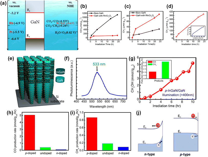 |
| | Fig. 24 (a) Band edge positions of GaN in comparison with the work function of Rh and Pt. CO2/CO and CO2/CH4 reduction potentials vs. normal hydrogen electrode for pH = 7 are shown together. Photocatalytic CO2 reduction reaction to (b) CO and (c) CH4 by Rh/Cr2O3 cocatalysts. (d) CH4 evolution over Pt-decorated GaN nanowires and the inset shows CO generation. Reproduced with permission from ref. 208. Copyright (2015) American Chemical Society. (e) Schematic of p-InGaN/GaN nanowire photocatalysts decorated with Pt nanoparticles. (f) Photoluminescence spectrum of InGaN/GaN photocatalysts. (g) CH3OH evolution over Pt-decorated p-InGaN/GaN nanowires under visible light illumination (>400 nm). The inset shows the production rates of CO and CH4. Doping-type-dependent production rate of (h) CO and (i) CH4 of InGaN/GaN nanowires. (j) Schematic of charge carrier transfer illustrated on n- (p-) doped semiconductors with upward (downward) surface band bending. Reproduced with permission from ref. 209. Copyright (2016) American Chemical Society. | |
Table 5 III-Nitride photocatalysts for photocatalytic CO2 conversion reaction
| Photocatalyst |
Cocatalyst |
Reactant |
Light source |
Performance |
Ref. |
| GaN NWs |
Pt |
CO2 + vaporized H2O |
300 W Xe lamp |
CH4 ∼14.8 μmol gcat−1 h−1 |
208
|
| p-InGaN/GaN NWs |
Pt |
CO2 + H2 + vaporized H2O |
300 W Xe lamp with 400 nm long-pass filter |
CH3OH ∼0.5 mmol gcat−1 h−1 |
209
|
| InGaN/GaN NWs |
Au@Cr2O3 |
CO2 + vaporized H2O |
300 W Xe lamp |
Syngas of 1.08 mol gcat−1 h−1 |
210
|
InGaN nanowires with narrower band gap can broaden the wavelength of light absorption and enhance the production rate compared to GaN nanowires. Hence, p-InGaN/GaN nanowires were grown on an Si substrate with the decoration of Pt nanoparticle cocatalysts for the photocatalytic CO2 conversion reaction (Fig. 24e).209 Photoluminescence spectroscopy measurement identified that the p-InGaN/GaN nanowire photocatalyst is capable of harvesting visible light (<533 nm) (Fig. 24f). The photocatalyst achieved a conversion rate of CO2 into CH3OH of ∼0.5 mmol gcat−1 h−1 under visible light illumination (>400 nm). Moreover, the role of dopants in the photocatalytic CO2 reduction reaction was investigated (Fig. 24g). Mg-doped InGaN nanowires presented much higher CO, CH4, and CH3OH production rates than the undoped and Ge-doped InGaN nanowires (Fig. 24h and i) because of the reduced surface potential barriers by downward band bending as well as the activation of the CO2 molecule (Fig. 24j). A mechanistic understanding of the origins for the enhanced photocatalytic activities provides insights into the important function of dopants and surface band bending of III-nitrides.
Recently, Au/Cr2O3 core/shell nanoparticle cocatalysts have shown promising photocatalytic CO2-to-CO conversion reactivity on 1D InGaN/GaN nanowires (Fig. 25a).210 Under solar irradiation, CO2 and H2O reactants were effectively converted to CO and H2 syngas with a production rate of 1.08 mol gcat−1 h−1 and a ratio of 1:1.6 (Fig. 25b). Au/Cr2O3 cocatalysts significantly outperform the single-component cocatalysts of Au and Cr2O3, evidencing the synergistic interaction between Au and Cr2O3 for photocatalytic reactions. Density functional calculation revealed that the CO2 molecule barely interacts with Au and the Cr2O3 surface while it is easily activated by bending the O–C–O angle to 116.5° on Au/Cr2O3, thus significantly reducing the reaction energy barrier (Fig. 25c). In addition, the energy barrier for the H2 evolution reaction was also lowest on the Au/Cr2O3 interface, exhibiting high catalytic activity for both CO and H2 evolution reactions and thus syngas synthesis (Fig. 25d and e).
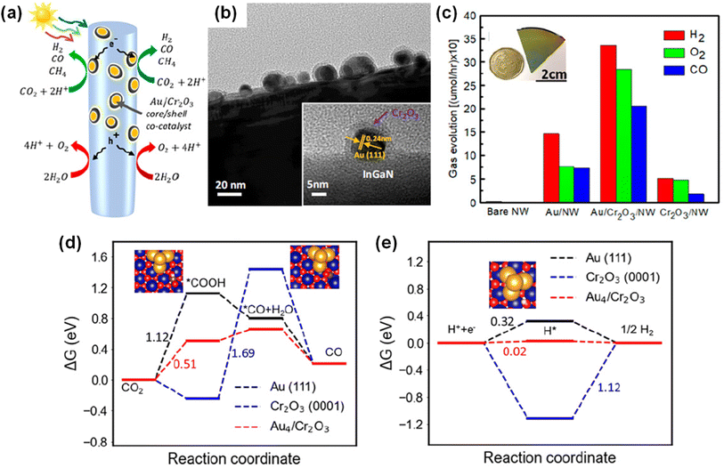 |
| | Fig. 25 (a) Schematic illustration of photocatalytic overall CO2 reduction reaction over Au/Cr2O3-decorated InGaN/GaN nanowires. (b) Structural analysis of Au/Cr2O3 core/shell cocatalysts on InGaN/GaN nanowires. (c) Output gas evolution with various cocatalysts. Calculated free energy diagrams for (d) CO2 reduction reaction and (e) H2 evolution reaction on different photocatalysts. Au, gold; Cr, blue; C, brown; and O, red. Reproduced with permission from ref. 210. Copyright (2022) National Academy of Science. | |
7. Challenges, prospects, and conclusions
III-Nitrides, e.g., InGaN, have tunable band gap energy and ideal band edge positions for water splitting and CO2 reduction. Moreover, the emerging 1D III-nitride nanostructures have greatly improved the performance of photoelectrodes and photocatalysts compared to the planar structures. In this review, we describe the fabrication methods of 1D III-nitrides and their application to photoelectrochemical and photocatalytic water splitting and CO2 reduction reactions, along with efficiency-enhancement strategies. There have been key challenges to artificial photosynthesis, such as (1) low optical absorption, (2) severe electron–hole recombination, (3) poor catalytic activity, and (4) poor stability. Thus, tuning of band gap energy for broadband light absorption is a primary concern to achieve a high yield of target products. In this context, indium incorporation into GaN nanowires and heterogeneous tandem stacking of dual- or triple-band III-nitrides have been demonstrated. Preventing the recombination of photogenerated electrons and holes is another critical issue for the efficient utilization of charge carriers. Therefore, electrical conductivity, surface band bending, and charge carrier transport properties have been finely controlled by n- or p-type doping of III-nitrides. The intrinsic catalytic activity and selectivity of III-nitrides could be enhanced by decoration with suitable cocatalysts, which sometimes show unprecedented synergy at the interface of the III-nitride/cocatalyst and realize a unique catalytic performance for water splitting and CO2 reduction reaction. Moreover, N-terminated top and lateral surfaces of GaN nanowires showed record-high stability over 3000 h for photoelectrochemical water splitting under solar light irradiation. Recent studies identified that the partial substitution of nitrogen by oxygen on the nonpolar lateral surface of GaN nanowire not only improves the catalytic activity for the H2 evolution reaction but is also responsible for the excellent stability against harsh reaction conditions.
Nevertheless, the state-of-the-art growth methods of high-crystal-quality III-nitrides are limited to wafer-scale fabrication techniques (e.g., MBE or MOCVD), which may pose limitations on the large-scale application of photocatalysts or photoelectrodes. Recent studies, however, found that concentrated solar light irradiation on wafer-scale 1D III-nitrides drastically improves their photocatalytic activity, which outperforms photocatalyst particles dispersed in the solution.149 Hence, the utilization of thermal energy obtained from phonon vibration or non-radiative recombination under concentrated sunlight has been attracting attention. The thermal energy generally degrades the optoelectronic properties of semiconductors but promotes the chemical reactions by providing additional energy to overcome the activation barriers. Considering these trade-offs, the rational design of III-nitrides and the careful utilization of the photoexcited charge carriers with photoinduced thermal energy will represent a significant opportunity. In addition, fast reaction kinetics under concentrated solar light will lead to a vigorous generation of products and consumption of reactants near the electrode, which will change the local reaction environment and affect catalytic activity and stability. The local shift in reaction condition near the III-nitrides may oxidize the specific crystal planes, leading to new composites on the surface. An understanding of the material, optoelectronic, and catalytic properties of the reconstructed surface compounds will guide us to design more efficient and stable III-nitride devices. Gas bubbles generated in the solution have the physical force to remove 1D III-nitrides from the substrate by surface tension. When the reaction rate increases under concentrated sunlight, the physical stability will become a more severe issue, and a strategy to anchor 1D nitride nanostructures on supports will be required. The stability of the photo(electro)catalyst is also largely dependent on the stability of the cocatalyst, and the separation of the cocatalyst from III-nitrides during the reaction has been a major reason for degradation. In general, since metallic nanoclusters or single-atom catalysts tend to be stably located in the N-vacancy of the nitride materials,211 the method of forming the N-vacancy and sub-nanometer cocatalysts on the surface of the III-nitride semiconductors as well as catalytic activity should be studied to hold the cocatalysts on the surface and to maintain high efficiency. To date, the growth of high-crystal-quality 1D III-nitrides has been limited to a few types of substrate due to lattice mismatch and high-temperature compatability of the substrate. Overcoming challenges in the growth method could potentially solve the efficiency bottleneck by integrating 1D III-nitrides with other highly efficient semiconductors (e.g., III–V semiconductors).
The fact that 1D III-nitrides are efficient and stable materials for water splitting and CO2 reduction reactions implies that these nanostructured semiconductors can also be used for various other chemical reactions, including ammonia (NH3) synthesis, methane (CH4) oxidation, and urea synthesis. Recently, studies related to the conversion of N2 or NO3− into NH3 in an aqueous solution are attracting great attention in order to replace the conventional energy-intensive and CO2-emissive synthetic process. However, the initial activation of these reactants is extremely difficult due to the difficulties of N![[triple bond, length as m-dash]](https://www.rsc.org/images/entities/char_e002.gif) N bond or N
N bond or N![[double bond, length as m-dash]](https://www.rsc.org/images/entities/char_e001.gif) O bond cleavage. This problem could be resolved if 1D III-nitrides with an appropriate amount of N-vacancies, that readily interact with N-containing reactants to activate and promote the catalytic reaction, could be realized.212 Moreover, unique metal–support interactions, found in the cocatalyst–III-nitride system, will broaden the application of 1D III-nitrides to solar-driven CH4 oxidation. Several promising results of CH4 oxidation to CH3OH213 and benzene production214via C–C coupling have been reported using 1D III-nitride artificial photosynthetic devices. Therefore, III-nitrides hold great potential for many solar-powered catalytic reactions by enhanced NN and NO bond cleavage, C–H bond activation, C–C and C–N coupling reactions, and aromatization.
O bond cleavage. This problem could be resolved if 1D III-nitrides with an appropriate amount of N-vacancies, that readily interact with N-containing reactants to activate and promote the catalytic reaction, could be realized.212 Moreover, unique metal–support interactions, found in the cocatalyst–III-nitride system, will broaden the application of 1D III-nitrides to solar-driven CH4 oxidation. Several promising results of CH4 oxidation to CH3OH213 and benzene production214via C–C coupling have been reported using 1D III-nitride artificial photosynthetic devices. Therefore, III-nitrides hold great potential for many solar-powered catalytic reactions by enhanced NN and NO bond cleavage, C–H bond activation, C–C and C–N coupling reactions, and aromatization.
In summary, various physical/chemical studies on 1D III-nitride semiconductors have led to the successful demonstration of artificial photosynthetic devices. A deeper understanding of the mechanism at the atomic scale with the assistance of experimental evaluation, catalyst characterization, operando analysis, advanced molecular dynamics and first-principals density functional calculations will provide further fundamental guidelines on the rational design of the device. In the near future, research on III-nitrides which can operate in extreme environments (i.e., high temperature, concentrated solar light, etc.) will be required to increase yield as well as efficiency and stability. Finally, since III-nitrides are one of the most commonly used semiconductor materials in the industry, commercialization is expected to be easier than for other competing materials if the III-nitride artificial photosynthesis device achieves an appropriate level of efficiency and lifetime.
Conflicts of interest
Some IP related to this work was licensed to NS Nanotech, Inc. and NX Fuels, Inc., which were co-founded by Z. Mi. The University of Michigan and Mi have a financial interest in NS Nanotech.
Acknowledgements
This work was supported by United States Army Research Office Award W911NF2110337.
References
- J. A. Turner, Science, 2004, 305, 972–974 CrossRef CAS PubMed.
- S. Chu and A. Majumdar, Nature, 2012, 488, 294–303 CrossRef CAS PubMed.
- O. S. Bushuyev, P. De Luna, C. T. Dinh, L. Tao, G. Saur, J. van de Lagemaat, S. O. Kelley and E. H. Sargent, Joule, 2018, 2, 825–832 CrossRef CAS.
- I. Sullivan, A. Goryachev, I. A. Digdaya, X. Li, H. A. Atwater, D. A. Vermaas and C. Xiang, Nat. Catal., 2021, 4, 952–958 CrossRef CAS.
- M. G. Walter, E. L. Warren, J. R. McKone, S. W. Boettcher, Q. Mi, E. A. Santori and N. S. Lewis, Chem. Rev., 2010, 110, 6446–6473 CrossRef CAS PubMed.
- Y. Tachibana, L. Vayssieres and J. R. Durrant, Nat. Photonics, 2012, 6, 511–518 CrossRef CAS.
- Y. He, T. Hamann and D. Wang, Chem. Soc. Rev., 2019, 48, 2182–2215 RSC.
- X. Li, J. Yu, M. Jaroniec and X. Chen, Chem. Rev., 2019, 119, 3962–4179 CrossRef CAS PubMed.
- C. E. Creissen and M. Fontecave, Adv. Energy Mater., 2021, 11, 2002652 CrossRef CAS.
- Y. Xia, P. Yang, Y. Sun, Y. Wu, B. Mayers, B. Gates, Y. Yin, F. Kim and H. Yan, Adv. Mater., 2003, 15, 353–389 CrossRef CAS.
- S. Barth, F. Hernandez-Ramirez, J. D. Holmes and A. Romano-Rodriguez, Prog. Mater. Sci., 2010, 55, 563–627 CrossRef CAS.
- M. Meng, L. Wang, C. Li, K. Xu, Y. Chen, J. Li, Z. Gan, H. Yuan, L. Liu and J. Li, Appl. Catal., B, 2023, 321, 122071 CrossRef CAS.
- W. J. Dong, C. J. Yoo, H. W. Cho, K. B. Kim, M. Kim and J. L. Lee, Small, 2015, 11, 1947–1953 CrossRef CAS PubMed.
- E. Garnett and P. Yang, Nano Lett., 2010, 10, 1082–1087 CrossRef CAS PubMed.
- D. A. Wheeler, G. Wang, Y. Ling, Y. Li and J. Z. Zhang, Energy Environ. Sci., 2012, 5, 6682–6702 RSC.
- F. X. Xiao, J. Miao, H. B. Tao, S. F. Hung, H. Y. Wang, H. B. Yang, J. Chen, R. Chen and B. Liu, Small, 2015, 11, 2115–2131 CrossRef CAS PubMed.
- J.-W. Lee, K.-H. Cho, J.-S. Yoon, Y.-M. Kim and Y.-M. Sung, J. Mater. Chem. A, 2021, 9, 21576–21606 RSC.
- B. Weng, S. Liu, Z.-R. Tang and Y.-J. Xu, RSC Adv., 2014, 4, 12685–12700 RSC.
- M. Kibria and Z. Mi, J. Mater. Chem. A, 2016, 4, 2801–2820 RSC.
- Y.-K. Kuo, B.-T. Liou, S.-H. Yen and H.-Y. Chu, Opt. Commun., 2004, 237, 363–369 CrossRef CAS.
- Y. Wu, X. Liu, A. Pandey, P. Zhou, W. J. Dong, P. Wang, J. Min, P. Deotare, M. Kira and E. Kioupakis, Prog. Quantum Electron., 2022, 100401 CrossRef.
- M. G. Kibria, R. Qiao, W. Yang, I. Boukahil, X. Kong, F. A. Chowdhury, M. L. Trudeau, W. Ji, H. Guo and F. Himpsel, Adv. Mater., 2016, 28, 8388–8397 CrossRef CAS PubMed.
- Z. H. Lan, C. H. Liang, C. W. Hsu, C. T. Wu, H. M. Lin, S. Dhara, K. H. Chen, L. C. Chen and C.-C. Chen, Adv. Funct. Mater., 2004, 14, 233–237 CrossRef CAS.
- J. Hu, Y. Bando, D. Golberg and Q. Liu, Angew. Chem., 2003, 115, 3617–3621 CrossRef.
- M. Kumar, S. Kumar, N. Chauhan, D. S. Kumar, V. Kumar and R. Singh, Semicond. Sci. Technol., 2017, 32, 085012 CrossRef.
- W.-S. Jung and B.-K. Min, Mater. Lett., 2004, 58, 3058–3062 CrossRef CAS.
- A. R. Wagner and S. W. Ellis, Appl. Phys. Lett., 1964, 4, 89–90 CrossRef.
- X. Duan and C. M. Lieber, J. Am. Chem. Soc., 2000, 122, 188–189 CrossRef CAS.
- Y. Tang, Z. Chen, H. Song, C. Lee, H. Cong, H. Cheng, W. Zhang, I. Bello and S. Lee, Nano Lett., 2008, 8, 4191–4195 CrossRef CAS PubMed.
- T. Kuykendall, P. J. Pauzauskie, Y. Zhang, J. Goldberger, D. Sirbuly, J. Denlinger and P. Yang, Nat. Mater., 2004, 3, 524–528 CrossRef CAS PubMed.
- C. B. Maliakkal, N. Hatui, R. D. Bapat, B. A. Chalke, A. A. Rahman and A. Bhattacharya, Nano Lett., 2016, 16, 7632–7638 CrossRef CAS PubMed.
- F. Qian, Y. Li, S. Gradečak, H.-G. Park, Y. Dong, Y. Ding, Z. L. Wang and C. M. Lieber, Nat. Mater., 2008, 7, 701–706 CrossRef CAS PubMed.
- C. Chèze, L. Geelhaar, B. Jenichen and H. Riechert, Appl. Phys. Lett., 2010, 97, 153105 CrossRef.
- T. R. Kuykendall, M. V. P. Altoe, D. F. Ogletree and S. Aloni, Nano Lett., 2014, 14, 6767–6773 CrossRef CAS PubMed.
- G. Avit, K. Lekhal, Y. André, C. Bougerol, F. Reveret, J. Leymarie, E. Gil, G. Monier, D. Castelluci and A. Trassoudaine, Nano Lett., 2014, 14, 559–562 CrossRef CAS PubMed.
- T. Kuykendall, P. Pauzauskie, S. Lee, Y. Zhang, J. Goldberger and P. Yang, Nano Lett., 2003, 3, 1063–1066 CrossRef CAS.
- B. Kuppulingam, R. Loganathan, K. Prabakaran and K. Baskar, Optik, 2016, 127, 3762–3765 CrossRef CAS.
- B. Alloing and J. Zúñiga-Pérez, Mater. Sci. Semicond. Process., 2016, 55, 51–58 CrossRef CAS.
- S. Zhao, H. P. Nguyen, M. G. Kibria and Z. Mi, Prog. Quantum Electron., 2015, 44, 14–68 CrossRef.
- C. Tessarek, S. Fladischer, C. Dieker, G. Sarau, B. Hoffmann, M. Bashouti, M. Göbelt, M. Heilmann, M. Latzel and E. Butzen, Nano Lett., 2016, 16, 3415–3425 CrossRef CAS PubMed.
- M. Knelangen, V. Consonni, A. Trampert and H. Riechert, Nanotechnology, 2010, 21, 245705 CrossRef CAS PubMed.
- K. A. Bertness, A. Roshko, L. Mansfield, T. E. Harvey and N. A. Sanford, J. Cryst. Growth, 2008, 310, 3154–3158 CrossRef CAS.
- Z. Xu, S. Zhang, F. Gao, L. Wen, Y. Yu and G. Li, Nanotechnology, 2018, 29, 475603 CrossRef PubMed.
- Y.-L. Chang, F. Li, A. Fatehi and Z. Mi, Nanotechnology, 2009, 20, 345203 CrossRef PubMed.
- V. Consonni, M. Hanke, M. Knelangen, L. Geelhaar, A. Trampert and H. Riechert, Phys. Rev. B: Condens. Matter Mater. Phys., 2011, 83, 035310 CrossRef.
- J. Shen, Y. Yu, J. Wang, Y. Zheng, Y. Gan and G. Li, Nanoscale, 2020, 12, 4018–4029 RSC.
- R. Debnath, R. Meijers, T. Richter, T. Stoica, R. Calarco and H. Lüth, Appl. Phys. Lett., 2007, 90, 123117 CrossRef.
- T. Stoica, E. Sutter, R. J. Meijers, R. K. Debnath, R. Calarco, H. Lüth and D. Grützmacher, Small, 2008, 4, 751–754 CrossRef CAS PubMed.
- V. Kumaresan, L. Largeau, A. Madouri, F. Glas, H. Zhang, F. Oehler, A. Cavanna, A. Babichev, L. Travers and N. Gogneau, Nano Lett., 2016, 16, 4895–4902 CrossRef CAS PubMed.
- A. Prabaswara, H. Kim, J.-W. Min, R. C. Subedi, D. H. Anjum, B. Davaasuren, K. Moore, M. Conroy, S. Mitra and I. S. Roqan, ACS Nano, 2020, 14, 2202–2211 CrossRef CAS PubMed.
- G. Calabrese, P. Corfdir, G. Gao, C. Pfüller, A. Trampert, O. Brandt, L. Geelhaar and S. Fernández-Garrido, Appl. Phys. Lett., 2016, 108, 202101 CrossRef.
- P. R. Narangari, S. K. Karuturi, M. Lysevych, H. H. Tan and C. Jagadish, Nanotechnology, 2017, 28, 154001 CrossRef PubMed.
- X. Xi, J. Li, Z. Ma, X. Li and L. Zhao, RSC Adv., 2019, 9, 14937–14943 RSC.
- Y. Sang, B. Liu, T. Tao, D. Jiang, Y. Wu, X. Chen, W. Luo, J. Ye and R. Zhang, Semicond. Sci. Technol., 2020, 35, 025017 CrossRef CAS.
- J. Butson, P. R. Narangari, S. K. Karuturi, R. Yew, M. Lysevych, H. H. Tan and C. Jagadish, Nanotechnology, 2017, 29, 045403 CrossRef PubMed.
- J. Y. Park, B. J. Kim, C. J. Yoo, W. J. Dong, I. Lee, S. Kim and J.-L. Lee, Sci. Rep., 2020, 10, 1–7 CrossRef CAS PubMed.
- J. H. Son, J. U. Kim, Y. H. Song, B. J. Kim, C. J. Ryu and J. L. Lee, Adv. Mater., 2012, 24, 2259–2262 CrossRef CAS PubMed.
- A. Pandey and Z. Mi, IEEE J. Quantum Electron., 2022, 58, 1–13 Search PubMed.
- K. Wang, G. Yuan, R. Wu, H. Lu, Z. Liu, T. Wei, J. Wang, J. Li and W. Zhang, J. Cryst. Growth, 2016, 440, 96–101 CrossRef CAS.
- X. Geng, B. K. Duan, D. A. Grismer, L. Zhao and P. W. Bohn, Electrochem. Commun., 2012, 19, 39–42 CrossRef CAS.
- J. Benton, J. Bai and T. Wang, Appl. Phys. Lett., 2014, 105, 223902 CrossRef.
- Y. Hou, Z. Ahmed Syed, L. Jiu, J. Bai and T. Wang, Appl. Phys. Lett., 2017, 111, 203901 CrossRef.
- S.-W. Ryu, Y. Zhang, B. Leung, C. Yerino and J. Han, Semicond. Sci. Technol., 2011, 27, 015014 CrossRef.
- J. Benton, J. Bai and T. Wang, Appl. Phys. Lett., 2013, 102, 173905 CrossRef.
- J. Benton, J. Bai and T. Wang, Appl. Phys. Lett., 2013, 103, 133904 CrossRef.
- M. Reddeppa, C. Thota, D.-J. Nam, H. Woo, S.-G. Kim and M.-D. Kim, Appl. Phys. Lett., 2021, 119, 023901 CrossRef CAS.
- M. Ebaid, J.-W. Min, C. Zhao, T. K. Ng, H. Idriss and B. S. Ooi, J. Mater. Chem. A, 2018, 6, 6922–6930 RSC.
- A. Abdullah, A. Waseem, I. V. Bagal, M. A. Johar, M. A. Kulkarni, J. K. Lee and S.-W. Ryu, ACS Appl. Energy Mater., 2021, 4, 13759–13765 CrossRef CAS.
- H. Bae, H. Rho, J.-W. Min, Y.-T. Lee, S. H. Lee, K. Fujii, H.-J. Lee and J.-S. Ha, Appl. Surf. Sci., 2017, 422, 354–358 CrossRef CAS.
- M. Ebaid, J.-H. Kang and S.-W. Ryu, Semicond. Sci. Technol., 2016, 32, 013001 CrossRef.
- M. Ebaid, J.-H. Kang and S.-W. Ryu, J. Electrochem. Soc., 2015, 162, H264 CrossRef CAS.
- S. Han, S. Noh, J. Shin, Y.-T. Yu, C.-R. Lee and J. S. Kim, J. Mater. Chem. C, 2021, 9, 12802–12810 RSC.
- A. Abdullah, I. V. Bagal, A. Waseem, M. A. Kulkarni, H. Thaalbi, J. K. Lee and S.-W. Ryu, Mater. Today Phys., 2022, 28, 100846 CrossRef CAS.
- B. AlOtaibi, M. Harati, S. Fan, S. Zhao, H. Nguyen, M. Kibria and Z. Mi, Nanotechnology, 2013, 24, 175401 CrossRef CAS PubMed.
- H. Chen, P. Wang, H. Ye, H. Yin, L. Rao, D. Luo, X. Hou, G. Zhou and R. Nötzel, Chem. Eng. J., 2021, 406, 126757 CrossRef CAS.
- H. Chen, P. Wang, X. Wang, X. Wang, L. Rao, Y. Qian, H. Yin, X. Hou, H. Ye and G. Zhou, Nano Energy, 2021, 83, 105768 CrossRef CAS.
- N. Alvi, P. Soto Rodriguez, P. Kumar, V. Gómez, P. Aseev, A. Alvi, M. Alvi, M. Willander and R. Nötzel, Appl. Phys. Lett., 2014, 104, 223104 CrossRef.
- H. Zhang, M. Ebaid, J.-W. Min, T. K. Ng and B. S. Ooi, J. Appl. Phys., 2018, 124, 083105 CrossRef.
- J. Lin, Y. Yu, Z. Xu, F. Gao, Z. Zhang, F. Zeng, W. Wang and G. Li, J. Power Sources, 2020, 450, 227578 CrossRef CAS.
- S. Chu, S. Vanka, Y. Wang, J. Gim, Y. Wang, Y.-H. Ra, R. Hovden, H. Guo, I. Shih and Z. Mi, ACS Energy Lett., 2018, 3, 307–314 CrossRef CAS.
- L. Caccamo, J. Hartmann, C. Fàbrega, S. Estrade, G. Lilienkamp, J. D. Prades, M. W. Hoffmann, J. Ledig, A. Wagner and X. Wang, ACS Appl. Mater. Interfaces, 2014, 6, 2235–2240 CrossRef CAS PubMed.
- B. AlOtaibi, H. Nguyen, S. Zhao, M. Kibria, S. Fan and Z. Mi, Nano Lett., 2013, 13, 4356–4361 CrossRef CAS PubMed.
- M. A. Hassan, J.-H. Kang, M. A. Johar, J.-S. Ha and S.-W. Ryu, Acta Mater., 2018, 146, 171–175 CrossRef CAS.
- Z. Xu, S. Zhang, F. Gao, P. Gao, Y. Yu, J. Lin, J. Liang and G. Li, Electrochim. Acta, 2019, 324, 134844 CrossRef CAS.
- S. Han, S. Noh, Y.-T. Yu, C.-R. Lee, S.-K. Lee and J. S. Kim, ACS Appl. Mater. Interfaces, 2020, 12, 58028–58037 CrossRef CAS PubMed.
- J. Lin, Y. Yu, Z. Zhang, F. Gao, S. Liu, W. Wang and G. Li, Adv. Funct. Mater., 2020, 30, 1910479 CrossRef CAS.
- S. Fan, I. Shih and Z. Mi, Adv. Energy Mater., 2017, 7, 1600952 CrossRef.
- D. Ghosh, P. Devi and P. Kumar, ACS Appl. Mater. Interfaces, 2020, 12, 13797–13804 CrossRef CAS PubMed.
- B. Zhou, X. Kong, S. Vanka, S. Chu, P. Ghamari, Y. Wang, N. Pant, I. Shih, H. Guo and Z. Mi, Nat. Commun., 2018, 9, 3856 CrossRef PubMed.
- S. Fan, B. AlOtaibi, S. Y. Woo, Y. Wang, G. A. Botton and Z. Mi, Nano Lett., 2015, 15, 2721–2726 CrossRef CAS PubMed.
- Y. Wang, Y. Wu, J. Schwartz, S. H. Sung, R. Hovden and Z. Mi, Joule, 2019, 3, 2444–2456 CrossRef CAS.
- Y. Wang, S. Vanka, J. Gim, Y. Wu, R. Fan, Y. Zhang, J. Shi, M. Shen, R. Hovden and Z. Mi, Nano Energy, 2019, 57, 405–413 CrossRef CAS.
- I. A. Navid, S. Vanka, R. A. Awni, Y. Xiao, Z. Song, Y. Yan and Z. Mi, Appl. Phys. Lett., 2021, 118, 243906 CrossRef CAS.
- S. Vanka, B. Zhou, R. A. Awni, Z. Song, F. A. Chowdhury, X. Liu, H. Hajibabaei, W. Shi, Y. Xiao and I. A. Navid, ACS Energy Lett., 2020, 5, 3741–3751 CrossRef CAS.
- G. Zeng, T. A. Pham, S. Vanka, G. Liu, C. Song, J. K. Cooper, Z. Mi, T. Ogitsu and F. M. Toma, Nat. Mater., 2021, 20, 1130–1135 CrossRef CAS PubMed.
- Y. Xiao, S. Vanka, T. A. Pham, W. J. Dong, Y. Sun, X. Liu, I. A. Navid, J. B. Varley, H. Hajibabaei and T. W. Hamann, Nano Lett., 2022, 22, 2236–2243 CrossRef CAS PubMed.
- S. Vanka, E. Arca, S. Cheng, K. Sun, G. A. Botton, G. Teeter and Z. Mi, Nano Lett., 2018, 18, 6530–6537 CrossRef CAS PubMed.
- Y. Wang, J. Schwartz, J. Gim, R. Hovden and Z. Mi, ACS Energy Lett., 2019, 4, 1541–1548 CrossRef CAS.
- W. J. Dong, Y. Xiao, K. R. Yang, Z. Ye, P. Zhou, I. A. Navid, V. S. Batista and Z. Mi, Nat. Commun., 2023, 14, 1–10 Search PubMed.
- H. Zhang, M. Ebaid, J. Tan, G. Liu, J.-W. Min, T. K. Ng and B. S. Ooi, Opt. Express, 2019, 27, A81–A91 CrossRef CAS PubMed.
- K. Aryal, B. Pantha, J. Li, J. Lin and H. Jiang, Appl. Phys. Lett., 2010, 96, 052110 CrossRef.
- J. Lin, W. Wang and G. Li, Adv. Funct. Mater., 2020, 30, 2005677 CrossRef CAS.
- M. Ebaid, J.-H. Kang, S.-H. Lim, J.-S. Ha, J. K. Lee, Y.-H. Cho and S.-W. Ryu, Nano Energy, 2015, 12, 215–223 CrossRef CAS.
- Y. J. Hwang, C. H. Wu, C. Hahn, H. E. Jeong and P. Yang, Nano Lett., 2012, 12, 1678–1682 CrossRef CAS PubMed.
- M. Ebaid, J.-H. Kang, S.-H. Lim, Y.-H. Cho and S.-W. Ryu, RSC Adv., 2015, 5, 23303–23310 RSC.
- J.-H. Park, A. Mandal, S. Kang, U. Chatterjee, J. S. Kim, B.-G. Park, M.-D. Kim, K.-U. Jeong and C.-R. Lee, Sci. Rep., 2016, 6, 1–10 CrossRef PubMed.
- E. Verlage, S. Hu, R. Liu, R. J. Jones, K. Sun, C. Xiang, N. S. Lewis and H. A. Atwater, Energy Environ. Sci., 2015, 8, 3166–3172 RSC.
- P. Varadhan, H.-C. Fu, Y.-C. Kao, R.-H. Horng and J.-H. He, Nat. Commun., 2019, 10, 1–9 CrossRef CAS PubMed.
- M. M. May, H.-J. Lewerenz, D. Lackner, F. Dimroth and T. Hannappel, Nat. Commun., 2015, 6, 1–7 Search PubMed.
- J. L. Young, M. A. Steiner, H. Döscher, R. M. France, J. A. Turner and T. G. Deutsch, Nat. Energy, 2017, 2, 1–8 Search PubMed.
- B. AlOtaibi, S. Fan, S. Vanka, M. Kibria and Z. Mi, Nano Lett., 2015, 15, 6821–6828 CrossRef CAS PubMed.
- C. W. Kim, S. J. Yeob, H.-M. Cheng and Y. S. Kang, Energy Environ. Sci., 2015, 8, 3646–3653 RSC.
- L. Wang, N. T. Nguyen, Z. Shen, P. Schmuki and Y. Bi, Nano Energy, 2018, 50, 331–338 CrossRef CAS.
- Z. Zhang, I. Karimata, H. Nagashima, S. Muto, K. Ohara, K. Sugimoto and T. Tachikawa, Nat. Commun., 2019, 10, 1–12 CrossRef PubMed.
- J. Zhang, P. Zhang, T. Wang and J. Gong, Nano Energy, 2015, 11, 189–195 CrossRef CAS.
- S. Wang, H. Chen, G. Gao, T. Butburee, M. Lyu, S. Thaweesak, J.-H. Yun, A. Du, G. Liu and L. Wang, Nano Energy, 2016, 24, 94–102 CrossRef CAS.
- J. Liu, S.-M. Xu, Y. Li, R. Zhang and M. Shao, Appl. Catal., B, 2020, 264, 118540 CrossRef CAS.
- H. S. Han, S. Shin, D. H. Kim, I. J. Park, J. S. Kim, P.-S. Huang, J.-K. Lee, I. S. Cho and X. Zheng, Energy Environ. Sci., 2018, 11, 1299–1306 RSC.
- C. W. Kim, Y. S. Son, M. J. Kang, D. Y. Kim and Y. S. Kang, Adv. Energy Mater., 2016, 6, 1501754 CrossRef.
- C. Li, Y. Li and J.-J. Delaunay, ACS Appl. Mater. Interfaces, 2014, 6, 480–486 CrossRef CAS PubMed.
- S. K. Baek, J. S. Kim, Y. D. Yun, Y. B. Kim and H. K. Cho, ACS Sustainable Chem. Eng., 2018, 6, 10364–10373 CrossRef CAS.
- H. Lee, W. Yang, J. Tan, Y. Oh, J. Park and J. Moon, ACS Energy Lett., 2019, 4, 995–1003 CrossRef CAS.
- W. Yang, J. Ahn, Y. Oh, J. Tan, H. Lee, J. Park, H. C. Kwon, J. Kim, W. Jo and J. Kim, Adv. Energy Mater., 2018, 8, 1702888 CrossRef.
- Z. Shi, J. Feng, H. Shan, X. Wang, Z. Xu, H. Huang, Q. Qian, S. Yan and Z. Zou, Appl. Catal., B, 2018, 237, 665–672 CrossRef CAS.
- Y. Hou, T. Li, S. Yan and Z. Zou, Appl. Catal., B, 2020, 269, 118777 CrossRef CAS.
- J. Luo, L. Steier, M.-K. Son, M. Schreier, M. T. Mayer and M. Grätzel, Nano Lett., 2016, 16, 1848–1857 CrossRef CAS PubMed.
- S. Choi, J. Hwang, T. H. Lee, H.-H. Kim, S.-P. Hong, C. Kim, M.-J. Choi, H. K. Park, S. S. Bhat and J. M. Suh, Chem. Eng. J., 2020, 392, 123688 CrossRef CAS.
- G. Wang, H. Wang, Y. Ling, Y. Tang, X. Yang, R. C. Fitzmorris, C. Wang, J. Z. Zhang and Y. Li, Nano Lett., 2011, 11, 3026–3033 CrossRef CAS PubMed.
- W.-H. Cheng, M. H. Richter, M. M. May, J. Ohlmann, D. Lackner, F. Dimroth, T. Hannappel, H. A. Atwater and H.-J. Lewerenz, ACS Energy Lett., 2018, 3, 1795–1800 CrossRef CAS.
- W. J. Dong, Y. J. Song, H. Yoon, G. H. Jung, K. Kim, S. Kim and J. L. Lee, Adv. Energy Mater., 2017, 7, 1700659 CrossRef.
- S. Chen and L.-W. Wang, Chem. Mater., 2012, 24, 3659–3666 CrossRef CAS.
- D. Bae, B. Seger, P. C. Vesborg, O. Hansen and I. Chorkendorff, Chem. Soc. Rev., 2017, 46, 1933–1954 RSC.
- S. Hu, M. R. Shaner, J. A. Beardslee, M. Lichterman, B. S. Brunschwig and N. S. Lewis, Science, 2014, 344, 1005–1009 CrossRef CAS PubMed.
- R. Fan, W. Dong, L. Fang, F. Zheng, X. Su, S. Zou, J. Huang, X. Wang and M. Shen, Appl. Phys. Lett., 2015, 106, 013902 CrossRef.
- S. Vanka, K. Sun, G. Zeng, T. A. Pham, F. M. Toma, T. Ogitsu and Z. Mi, J. Mater. Chem. A, 2019, 7, 27612–27619 RSC.
- P. Varadhan, H.-C. Fu, D. Priante, J. R. D. Retamal, C. Zhao, M. Ebaid, T. K. Ng, I. Ajia, S. Mitra and I. S. Roqan, Nano Lett., 2017, 17, 1520–1528 CrossRef CAS PubMed.
- T. Takata, J. Jiang, Y. Sakata, M. Nakabayashi, N. Shibata, V. Nandal, K. Seki, T. Hisatomi and K. Domen, Nature, 2020, 581, 411–414 CrossRef CAS PubMed.
- M. Ni, M. K. Leung, D. Y. Leung and K. Sumathy, Renewable Sustainable Energy Rev., 2007, 11, 401–425 CrossRef CAS.
- X. Guan, F. A. Chowdhury, N. Pant, L. Guo, L. Vayssieres and Z. Mi, J. Phys. Chem. C, 2018, 122, 13797–13802 CrossRef CAS.
- X. Guan, F. A. Chowdhury, Y. Wang, N. Pant, S. Vanka, M. L. Trudeau, L. Guo, L. Vayssieres and Z. Mi, ACS Energy Lett., 2018, 3, 2230–2231 CrossRef CAS.
- Q. Luo, R. Yuan, Y.-L. Hu and D. Wang, Appl. Surf. Sci., 2021, 537, 147930 CrossRef CAS.
- M. G. Kibria, H. P. Nguyen, K. Cui, S. Zhao, D. Liu, H. Guo, M. L. Trudeau, S. Paradis, A.-R. Hakima and Z. Mi, ACS Nano, 2013, 7, 7886–7893 CrossRef CAS PubMed.
- Y. Wang, Y. Wu, K. Sun and Z. Mi, Mater. Horiz., 2019, 6, 1454–1462 RSC.
- M. Kibria, F. Chowdhury, S. Zhao, M. Trudeau, H. Guo and Z. Mi, Appl. Phys. Lett., 2015, 106, 113105 CrossRef.
- M. Kibria, S. Zhao, F. Chowdhury, Q. Wang, H. Nguyen, M. Trudeau, H. Guo and Z. Mi, Nat. Commun., 2014, 5, 1–6 Search PubMed.
- M. Kibria, F. Chowdhury, S. Zhao, B. AlOtaibi, M. Trudeau, H. Guo and Z. Mi, Nat. Commun., 2015, 6, 1–8 Search PubMed.
- F. A. Chowdhury, M. L. Trudeau, H. Guo and Z. Mi, Nat. Commun., 2018, 9, 1–9 CrossRef CAS PubMed.
- Z. Li, L. Zhang, Y. Liu, C. Shao, Y. Gao, F. Fan, J. Wang, J. Li, J. Yan and R. Li, Angew. Chem., Int. Ed., 2020, 59, 935–942 CrossRef CAS PubMed.
- P. Zhou, I. A. Navid, Y. Ma, Y. Xiao, P. Wang, Z. Ye, B. Zhou, K. Sun and Z. Mi, Nature, 2023, 613, 66–70 CrossRef CAS PubMed.
- D. Wang, A. Pierre, M. G. Kibria, K. Cui, X. Han, K. H. Bevan, H. Guo, S. Paradis, A.-R. Hakima and Z. Mi, Nano Lett., 2011, 11, 2353–2357 CrossRef CAS PubMed.
- S. Barbet, R. Aubry, M.-A. di Forte-Poisson, J.-C. Jacquet, D. Deresmes, T. Melin and D. Théron, Appl. Phys. Lett., 2008, 93, 212107 CrossRef.
- H. Sezen, E. Ozbay, O. Aktas and S. Suzer, Appl. Phys. Lett., 2011, 98, 111901 CrossRef.
- M. Seelmann-Eggebert, J. Weyher, H. Obloh, H. Zimmermann, A. Rar and S. Porowski, Appl. Phys. Lett., 1997, 71, 2635–2637 CrossRef CAS.
- G. Liu, F. Zheng, J. Li, G. Zeng, Y. Ye, D. M. Larson, J. Yano, E. J. Crumlin, J. W. Ager and L.-w. Wang, Nat. Energy, 2021, 6, 1124–1132 CrossRef CAS.
- B. Tang and F.-X. Xiao, ACS Catal., 2022, 12, 9023–9057 CrossRef CAS.
- D. Li, K. Yang, J. Lian, J. Yan and S. Liu, Adv. Energy Mater., 2022, 12, 2201070 CrossRef CAS.
- L. K. Putri, B. J. Ng, W. J. Ong, S. P. Chai and A. R. Mohamed, Adv. Energy Mater., 2022, 12, 2201093 CrossRef CAS.
- X. Chang, T. Wang, P. Yang, G. Zhang and J. Gong, Adv. Mater., 2019, 31, 1804710 CrossRef PubMed.
- P. Ding, T. Jiang, N. Han and Y. Li, Mater. Today Nano, 2020, 10, 100077 CrossRef.
- J. T. Song, H. Ryoo, M. Cho, J. Kim, J. G. Kim, S. Y. Chung and J. Oh, Adv. Energy Mater., 2017, 7, 1601103 CrossRef.
- C. Li, T. Wang, B. Liu, M. Chen, A. Li, G. Zhang, M. Du, H. Wang, S. F. Liu and J. Gong, Energy Environ. Sci., 2019, 12, 923–928 RSC.
- N. Sagara, S. Kamimura, T. Tsubota and T. Ohno, Appl. Catal., B, 2016, 192, 193–198 CrossRef CAS.
- S. Zhou, K. Sun, J. Huang, X. Lu, B. Xie, D. Zhang, J. N. Hart, C. Y. Toe, X. Hao and R. Amal, Small, 2021, 17, 2100496 CrossRef CAS PubMed.
- W. J. Dong, J. W. Lim, D. M. Hong, J. Kim, J. Y. Park, W. S. Cho, S. Baek and J.-L. Lee, ACS Appl. Mater. Interfaces, 2021, 13, 18905–18913 CrossRef CAS PubMed.
- G. Zeng, J. Qiu, B. Hou, H. Shi, Y. Lin, M. Hettick, A. Javey and S. B. Cronin, Chem.–Eur. J., 2015, 21, 13502–13507 CrossRef CAS PubMed.
- M. Kan, C. Yang, Q. Wang, Q. Zhang, Y. Yan, K. Liu, A. Guan and G. Zheng, Adv. Energy Mater., 2022, 2201134 CrossRef CAS.
- S. Roy, M. Miller, J. Warnan, J. J. Leung, C. D. Sahm and E. Reisner, ACS Catal., 2021, 11, 1868–1876 CrossRef CAS.
- P. A. Kempler, M. H. Richter, W.-H. Cheng, B. S. Brunschwig and N. S. Lewis, ACS Energy Lett., 2020, 5, 2528–2534 CrossRef CAS.
- G. Liu, P. R. Narangari, Q. T. Trinh, W. Tu, M. Kraft, H. H. Tan, C. Jagadish, T. S. Choksi, J. W. Ager and S. Karuturi, ACS Catal., 2021, 11, 11416–11428 CrossRef CAS.
- J. Qiu, G. Zeng, M.-A. Ha, M. Ge, Y. Lin, M. Hettick, B. Hou, A. N. Alexandrova, A. Javey and S. B. Cronin, Nano Lett., 2015, 15, 6177–6181 CrossRef CAS PubMed.
- Y. Zhang, D. Pan, Y. Tao, H. Shang, D. Zhang, G. Li and H. Li, Adv. Funct. Mater., 2022, 32, 2109600 CrossRef CAS.
- K. Lee, S. Lee, H. Cho, S. Jeong, W. D. Kim, S. Lee and D. C. Lee, J. Energy Chem., 2018, 27, 264–270 CrossRef.
- H.-Y. Kang, D.-H. Nam, K. D. Yang, W. Joo, H. Kwak, H.-H. Kim, S.-H. Hong, K. T. Nam and Y.-C. Joo, ACS Nano, 2018, 12, 8187–8196 CrossRef CAS PubMed.
- X. Deng, R. Li, S. Wu, L. Wang, J. Hu, J. Ma, W. Jiang, N. Zhang, X. Zheng and C. Gao, J. Am. Chem. Soc., 2019, 141, 10924–10929 CrossRef CAS PubMed.
- Y. J. Jang, J.-W. Jang, J. Lee, J. H. Kim, H. Kumagai, J. Lee, T. Minegishi, J. Kubota, K. Domen and J. S. Lee, Energy Environ. Sci., 2015, 8, 3597–3604 RSC.
- J. S. DuChene, G. Tagliabue, A. J. Welch, W.-H. Cheng and H. A. Atwater, Nano Lett., 2018, 18, 2545–2550 CrossRef CAS PubMed.
- S. Chu, S. Fan, Y. Wang, D. Rossouw, Y. Wang, G. A. Botton and Z. Mi, Angew. Chem., Int. Ed., 2016, 55, 14262–14266 CrossRef CAS PubMed.
- S. Chu, P. Ou, P. Ghamari, S. Vanka, B. Zhou, I. Shih, J. Song and Z. Mi, J. Am. Chem. Soc., 2018, 140, 7869–7877 CrossRef CAS PubMed.
- S. Chu, P. Ou, R. T. Rashid, P. Ghamari, R. Wang, H. N. Tran, S. Zhao, H. Zhang, J. Song and Z. Mi, iScience, 2020, 23, 101390 CrossRef CAS PubMed.
- S. Chu, P. Ou, R. T. Rashid, Y. Pan, D. Liang, H. Zhang, J. Song and Z. Mi, Green Energy Environ., 2022, 7, 545–553 CrossRef CAS.
- W. J. Dong, P. Zhou, Y. Xiao, I. A. Navid, J.-L. Lee and Z. Mi, ACS Catal., 2022, 12, 2671–2680 CrossRef CAS.
- B. Zhou, X. Kong, S. Vanka, S. Cheng, N. Pant, S. Chu, P. Ghamari, Y. Wang, G. Botton and H. Cuo, Energy Environ. Sci., 2019, 12, 2842–2848 RSC.
- W. J. Dong, I. A. Navid, Y. Xiao, T. H. Lee, J. W. Lim, D. Lee, H. W. Jang, J.-L. Lee and Z. Mi, J. Mater. Chem. A, 2022, 10, 7869–7877 RSC.
- Y. Wang, S. Fan, B. AlOtaibi, Y. Wang, L. Li and Z. Mi, Chem.–Eur. J., 2016, 22, 8809–8813 CrossRef CAS PubMed.
- B. Zhou, P. Ou, N. Pant, S. Cheng, S. Vanka, S. Chu, R. T. Rashid, G. Botton, J. Song and Z. Mi, Proc. Natl. Acad. Sci. U. S. A., 2020, 117, 1330–1338 CrossRef CAS PubMed.
- W. J. Dong, I. A. Navid, Y. Xiao, J. W. Lim, J.-L. Lee and Z. Mi, J. Am. Chem. Soc., 2021, 143, 10099–10107 CrossRef CAS PubMed.
- S. Chu, R. T. Rashid, Y. Pan, X. Wang, H. Zhang and R. Xiao, J. CO2 Util., 2022, 60, 101993 CrossRef CAS.
- M. E. Dry, Catal. Today, 2002, 71, 227–241 CrossRef CAS.
- H. Schulz, Appl. Catal., A, 1999, 186, 3–12 CrossRef CAS.
- M. Azuma, K. Hashimoto, M. Hiramoto, M. Watanabe and T. Sakata, J. Electrochem. Soc., 1990, 137, 1772 CrossRef CAS.
- M. Jitaru, D. Lowy, M. Toma, B. Toma and L. Oniciu, J. Appl. Electrochem., 1997, 27, 875–889 CrossRef CAS.
- H. Li and C. Oloman, J. Appl. Electrochem., 2006, 36, 1105–1115 CrossRef CAS.
- Y. Hori, H. Wakebe, T. Tsukamoto and O. Koga, Electrochim. Acta, 1994, 39, 1833–1839 CrossRef CAS.
- R. Kortlever, I. Peters, S. Koper and M. T. Koper, ACS Catal., 2015, 5, 3916–3923 CrossRef CAS.
- W. J. Dong, C. J. Yoo and J.-L. Lee, ACS Appl. Mater. Interfaces, 2017, 9, 43575–43582 CrossRef CAS PubMed.
- C. J. Yoo, W. J. Dong, J. Y. Park, J. W. Lim, S. Kim, K. S. Choi, F. O. Odongo Ngome, S.-Y. Choi and J.-L. Lee, ACS Appl. Energy Mater., 2020, 3, 4466–4473 CrossRef CAS.
- W. J. Dong, J. W. Lim, D. M. Hong, J. Y. Park, W. S. Cho, S. Baek, C. J. Yoo, W. Kim and J.-L. Lee, ACS Appl. Energy Mater., 2020, 3, 10568–10577 CrossRef CAS.
- W. J. Dong, D. M. Hong, J. Y. Park, S. Kim, C. J. Yoo and J.-L. Lee, J. Electrochem. Soc., 2021, 168, 016514 CrossRef CAS.
- J. Kim, J. Y. Park, W. S. Cho, W. J. Dong, J. W. Lim, K. Kim, P. Fernández and J.-L. Lee, ACS Appl. Energy Mater., 2022, 5, 11042–11051 CrossRef CAS.
- W. J. Dong, J. W. Lim, J. Y. Park, C. J. Yoo, S. Baek, W. S. Cho, W. Kim and J.-L. Lee, Appl. Surf. Sci., 2021, 565, 150460 CrossRef CAS.
- W. S. Cho, D. M. Hong, W. J. Dong, T. H. Lee, C. J. Yoo, D. Lee, H. W. Jang and J. L. Lee, Energy Environ. Mater., 2022, e12490 Search PubMed.
- C. Xiao and J. Zhang, ACS Nano, 2021, 15, 7975–8000 CrossRef CAS PubMed.
- A. Loiudice, P. Lobaccaro, E. A. Kamali, T. Thao, B. H. Huang, J. W. Ager and R. Buonsanti, Angew. Chem., Int. Ed., 2016, 55, 5789–5792 CrossRef CAS PubMed.
- W. J. Dong, C. J. Yoo, J. W. Lim, J. Y. Park, K. Kim, S. Kim, D. Lee and J.-L. Lee, Nano Energy, 2020, 78, 105168 CrossRef CAS.
- J. W. Lim, W. J. Dong, W. S. Cho, C. J. Yoo and J.-L. Lee, ACS Catal., 2022, 12, 13174–13185 CrossRef CAS.
- J. W. Lim, W. J. Dong, J. Y. Park, D. M. Hong and J.-L. Lee, ACS Appl. Mater. Interfaces, 2020, 12, 22891–22900 CrossRef CAS PubMed.
- P. Hou, W. Song, X. Wang, Z. Hu and P. Kang, Small, 2020, 16, 2001896 CrossRef CAS PubMed.
- B. AlOtaibi, S. Fan, D. Wang, J. Ye and Z. Mi, ACS Catal., 2015, 5, 5342–5348 CrossRef CAS.
- B. AlOtaibi, X. Kong, S. Vanka, S. Woo, A. Pofelski, F. Oudjedi, S. Fan, M. Kibria, G. Botton and W. Ji, ACS Energy Lett., 2016, 1, 246–252 CrossRef CAS.
- R. T. Rashid, Y. Chen, X. Liu, F. A. Chowdhury, M. Liu, J. Song, Z. Mi and B. Zhou, Proc. Natl. Acad. Sci. U. S. A., 2022, 119, e2121174119 CrossRef CAS PubMed.
- W. H. Lai, Z. Miao, Y. X. Wang, J. Z. Wang and S. L. Chou, Adv. Energy Mater., 2019, 9, 1900722 CrossRef CAS.
- M. Liu, Y. Wang, X. Kong, L. Tan, L. Li, S. Cheng, G. Botton, H. Guo, Z. Mi and C.-J. Li, Iscience, 2019, 17, 208–216 CrossRef CAS PubMed.
- P. Zhou, I. A. Navid, Y. Xiao, Z. Ye, W. J. Dong, P. Wang, K. Sun and Z. Mi, J. Phys. Chem. Lett., 2022, 13, 8122–8129 CrossRef CAS PubMed.
- L. Li, S. Fan, X. Mu, Z. Mi and C.-J. Li, J. Am. Chem. Soc., 2014, 136, 7793–7796 CrossRef CAS PubMed.
|
| This journal is © The Royal Society of Chemistry 2023 |

 * and
Zetian
Mi
*
* and
Zetian
Mi
*