
 Open Access Article
 This Open Access Article is licensed under a Creative Commons Attribution-Non Commercial 3.0 Unported Licence
Electrochemical regulation of the band gap of single layer graphene: from semimetal to semiconductor
Lanping
Zeng
a,
Weiying
Song
a,
Xiangfeng
Jin
a,
Quanfeng
He
a,
Lianhuan
Han
 *a,
Yuan-fei
Wu
a,
Corinne
Lagrost
b,
Yann
Leroux
b,
Philippe
Hapiot
b,
Yang
Cao
*a,
Jun
Cheng
a and
Dongping
Zhan
*ac
*a,
Yuan-fei
Wu
a,
Corinne
Lagrost
b,
Yann
Leroux
b,
Philippe
Hapiot
b,
Yang
Cao
*a,
Jun
Cheng
a and
Dongping
Zhan
*ac
aState Key Laboratory of Physical Chemistry of Solid Surfaces (PCOSS), Fujian Science & Technology Innovation Laboratory for Energy Materials of China, Engineering Research Center of Electrochemical Technologies of Ministry of Education, Department of Chemistry, College of Chemistry and Chemical Engineering, Department of Mechanical and Electrical Engineering, School of Aerospace Engineering, Xiamen University, Xiamen 361005, China. E-mail: hanlianhuan@xmu.edu.cn; yangcao@xmu.edu.cn; dpzhan@xmu.edu.cn
bUniv. Rennes, CNRS, ISCR – UMR 6226, 35000 Rennes, France
cDepartment of Chemistry, College of Chemistry and Chemical Engineering, Ningxia University, Yinchuan 750021, China
First published on 17th March 2023
Abstract
As a semimetal with a zero band gap and single-atom-scale thickness, single layer graphene (SLG) has excellent electron conductivity on its basal plane. If the band gap could be opened and regulated controllably, SLG would behave as a semiconductor. That means electronic elements or even electronic circuits with single-atom thickness could be expected to be printed on a wafer-scale SLG substrate, which would bring about a revolution in Moore's law of integrated circuits, not by decreasing the feature size of line width, but by piling up the atomic-scale-thickness of an SLG circuit board layer by layer. Employing scanning electrochemical microscopy (SECM), we have demonstrated that the electrochemically induced brominating addition reaction can open and regulate the band gap of SLG by forming SLG bromide (SLGBr). The SLG/SLGBr/SLG Schottky junction shows excellent performance in current rectification, and the rectification potential region can be regulated by tuning the degree of bromination of SLG. This work provides a feasible and effective way to regulate the band gap of SLG, which would open new applications for SLG in micro–nano electronics and ultra-large-scale integrated circuits (ULSI).
Introduction
Graphene (Gr) is one of the most attractive two-dimensional (2D) materials with a zero band gap, a single-atom-scale thickness, and an excellent electronic property, providing a promising future for micro–nanoelectronics.1–4 However, the zero band gap qualifies Gr as a semimetal but not a semiconductor, which limits its applications in all-in-Gr electronic elements and electronic circuits.5,6 If its band gap could be opened and regulated, Gr could be changed into a semiconductor, providing possibilities for fabricating all-in-Gr diodes, triodes and field-effect transistors.7,8 If an electronic circuit could be “printed” directly on a single layer Gr (SLG) wafer, it would cause a revolution in Moore's law in the micro–nanoelectronics industry and ultra-large-scale integrated circuits (ULSI) by piling up the single-atom-thickness of an all-in-Gr circuit board layer by layer, not by reducing the feature size of the line width of the silicon-based electronic elements and copper interconnectors.For SLG to qualify as a material for electronic elements, it is crucial to open its band gap to 0.4 eV or higher at room temperature in order to ensure a sufficient on–off switch ratio.9,10 Great efforts have been made to achieve such a goal by either physical or chemical approaches.11 The advantage of a physical method is that it does not change the crystalline structure of SLG, but the reversal symmetry of the lattice of the double-layer or triple-layer SLG. Zhang et al. applied a vertical electric field to a double-layer SLG plane, and found that the band gap keeps increasing with the strength of the applied electric field until it arrives at a maximum of 0.25 eV.12 Zhou et al. measured a band gap of less than 0.20 eV caused by interaction between SLG and the silicon carbide (SiC) substrate. However, conflicts exist because the results of theoretical calculations show that the SLG still has a zero band gap.13 Schwierz et al. reported that if the width of an SLG nano-ribbon was decreased to 10 nm or less, the band gap could be made greater than 0.4 eV due to the quantum confinement effect of charge transport.14 Other strategies, based on the spin–orbit coupling effect,15,16 stretching stress,17 physical adsorption,18etc., have also been tried. In general, the biggest disadvantage of a physical method is the narrow and unstable band gap. In some cases, extra physical-field regulation is needed to maintain the band gap, e.g., an electric field or a stretching stress. The band gap will go back to zero again if the extra physical-fields are removed. On the other hand, as for physical modulation, the controllable mass production of SLG electric elements has a long way to go.
Using principles other than physical methods, in order to open a band gap in SLG, chemical methods introduce sp3-defects by surface modification and element doping. Chemical interactions, such as chemical doping19,20 or surface adsorption, between SLG and atomic hydrogen,21 fluorine22 or oxygen species,23 have been reported. Ideally, if SLG is totally hydrogenated to form graphene, the latter will have a band gap bigger than 3.50 eV,24 leaving a large space to open and regulate the band gap of SLG. Elias et al. treated SLG with hydrogen plasma to form hydride SLG, which transforms the highly conductive semimetal into an insulator.25 Unfortunately, it changed back into pristine SLG after thermal annealing, indicating instability of the carbon–hydrogen interaction. Doping SLG with boron, nitrogen, silicon or phosphorus has also been tried. Zhang et al. doped SLG with silicon (Si) by chemical vapor deposition (CVD) and found that the band gap could reach 0.28 eV.20 By theoretical calculation, the authors determined an atomic ratio of Si of 3.1%. Nevertheless, the main issues are the weak stability, and the harsh conditions or advanced equipment required for chemical doping. To solve the problem of instability, a promising approach is to form strong covalent bonds between the carbon atoms and the foreign atoms through chemical reactions, meanwhile not changing the crystalline integrity of SLG, rather than chemical doping or surface adsorption.
We have previously demonstrated the feasibility of radical addition for the functionalization of Gr. For example, we proposed a strategy to extend the lifetime of the hydroxyl radical (OH˙), and to facilitate an OH˙ radical addition reaction with Gr for the high-efficiency electrochemical production of Gr oxide.26 Here, we found that bromide (Br−) oxidation to bromine (Br or Br2) on SLG forms highly stable brominated SLG (SLGBr) through an addition reaction. Using this reaction, the band gap of SLGBr can easily be opened and controlled by tuning the degree of bromination. We also fabricated all-in-Gr SLG diodes and investigated their current rectification performance.
Results and discussion
As depicted in Fig. 1a, an SLG microstrip with two gold (Au) terminals works as the working electrode, a micropipette containing an aqueous solution with 10 mM KBr and 10 mM H2SO4 was employed as the electrolyte cell, and platinum (Pt) as the quasi-reference electrode and counter electrode, is fixed on the midpoint of the microstrip to construct an electrochemical system by the SECM manipulator. As shown in Fig. 1b, the voltammetric behavior of the bromide anion (Br−) on the SLG microstrip electrode corresponds to an irreversible electrode process because, unlike a Pt electrode, carbon materials are not known as good electrocatalysts for the redox reaction of halide anions. The anodic peak potential of Br− oxidation is observed at 1.1 V and the cathodic peak potential of Br2 reduction is observed at −0.2 V vs. the Pt-wire quasi-reference electrode. A distinct but interesting phenomenon should be noted: both anodic current and cathodic current keep decreasing during the sequential scan cycles, suggesting that the SLG microstrip electrode is losing its electroactivity, hence predicting the occurrence of a brominating addition reaction between SLG and the electrogenerated bromine species. In principle, atomic bromine (Br) should be more reactive than molecular bromine (Br2) because the latter involves extra energy for the breakage of the Br–Br covalent bond in the brominating addition reaction with SLG. Thus, it is reasonable to formulate the anodic process on the SLG working electrode as follows:| Br− → Br + e− | (1) |
| SLG + Br → SLGBr | (2) |
| 2Br → Br2 | (3) |
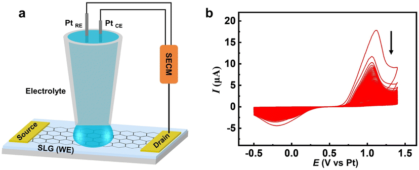 | ||
| Fig. 1 (a) Schematic diagram of SLG bromination process. (b) Cyclic voltammograms of SLG microstrip electrode in an aqueous solution with 10 mM KBr and 10 mM H2SO4; the scan rate is 100 mV s−1. | ||
And the cathodic process on the SLG microstrip electrode is attributed to the electrochemical reduction of excessive Br2 which does not react with SLG in time:
| Br2 + 2e → 2Br− | (4) |
The advantage of cyclic voltammetry over chronoamperometry and chronopotentiometry lies in the unreacted Br2 being able to be reduced to Br− and diffuse into the solution, and the adsorption of Br2 and Br− can be well avoided at the negative potentials. Thus, clean SLG/SLGBr/SLG microstrips can be obtained, which will be further demonstrated by the XPS characterization.
To identify the occurrence of an electrochemically induced brominating addition reaction, Raman experiments were first performed to detect the sp3-defect contents of the SLGBr area. Fig. 2a displays the Raman images of pristine SLG and SLGBr after 50, 100 and 150 cycles of brominating procedure by cyclic voltammetry. They clearly show that the degree of bromination can be well controlled by the potential-scan cycles. Fig. 2b shows the corresponding Raman spectra of the three SLGBr patterns and pristine SLG. The black line shows a typical Raman spectrum of pristine SLG with a G-peak at ∼1580 cm−1 and a 2D peak at ∼2680 cm−1. The 2D peak is symmetric and its intensity is much stronger than that of the G peak. The absence of the D peak confirms the high quality of the SLG sample.27 After the brominating process, the D (∼1350 cm−1) and D′ (∼1620 cm−1) peaks, which only appear in defective Gr,28,29 were observed and their intensities increased with the increasing number of potential–scan cycles. The intensity ratio (ID/IG), which is regarded as a criterion for the ratio of non-sp2 to sp2 bonding character for carbon-based materials,30 increases from 0.93 to 2.71 as the duration of bromination varies from 50 to 150 cycles. The ID'/ID ratio also increases from 0.18 to 0.51, indicating that the sp3-C content of the SLGBr crystalline structure increases with the increased potential-scan cycles.
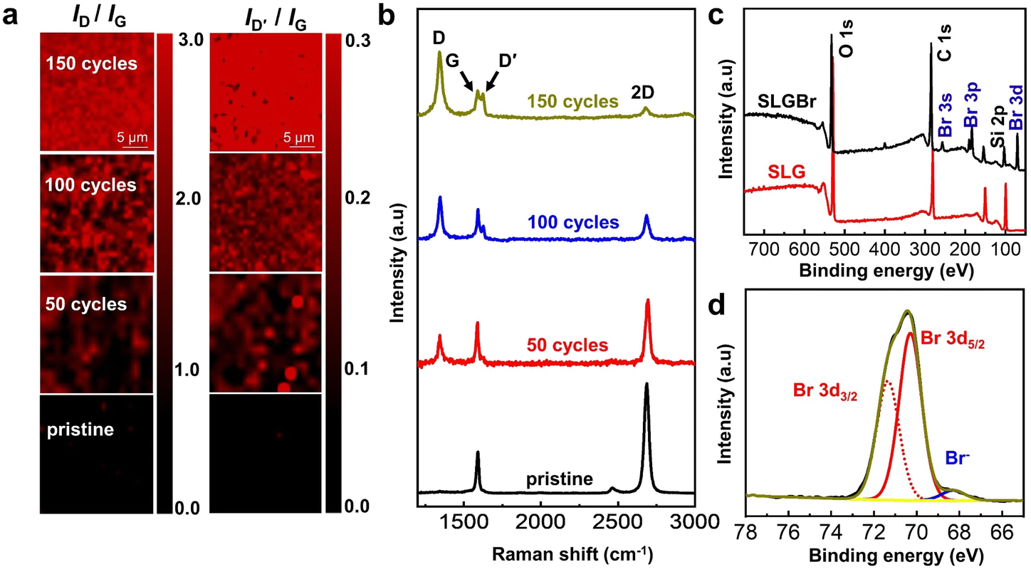 | ||
| Fig. 2 (a) Raman mapping of the intensity ratio ID/IG and ID'/IG with the same scale bar. (b) The corresponding Raman spectra of SLG with different degrees of bromination. (c) XPS spectrum of SLG and SLGBr before and after bromination. (d) High-resolution XPS spectrum of Br 3d in SLGBr. | ||
XPS experiments were performed to identify the carbon–bromine (C–Br) functionalization of the SLG surface. In Fig. 2c, the characteristic photoelectron peaks of C 1s, O 1s and Si elements can clearly be observed. The peaks at 103 eV (Si 2p) and 154 eV (Si 2s) are related to the SiO2/Si substrate. In the case of SLGBr, new characteristic peaks appeared due to the bromination process, which are attributed to Br 3s at 257 eV, Br 3p at 183 eV and Br 3d at 70 eV,31 respectively. The high-resolution XPS spectrum for the Br 3d signal is shown in Fig. 2d. The Br 3d peak can be fitted into a pair of peaks at 70.3 eV and 71.3 eV, which is caused by spin–orbit splitting that leads to a doublet structure of Br 3d5/2 and Br 3d3/2. This signal indicates the formation of a covalent C–Br bond.32 It should be noted that, because the final potential of cyclic voltammetry was set at −0.5 V during the bromination process, there should be little residual Br2 on the SLG strip. However, a very weak XPS peak is observed at about 68.5 eV, which might be due to a trace amount of adsorbed Br−. All the above results demonstrate the occurrence of an electrochemically induced brominating addition reaction and that the SLG can be brominated to form SLGBr with a different degree of bromination by tuning the potential-scan cycles.
SLG/SLGBr/SLG diodes with different degrees of bromination were prepared, as depicted in Fig. 3a. The current Ids was measured and plotted as a function of Vds, as shown in Fig. 3b. The pristine SLG strip exhibits a linear Ids–Vds curve (black line) which reflects the typical electrical properties of a pure resistor. However, the SLG/SLGBr/SLG devices show a quite different nonlinear Ids–Vds response, such as the red, blue and green curves which correspond to the diodes obtained with bromination processes of 50, 100 and 150 potential-scan cycles. Similar to a previous report on Gr nanoribbons,33 the electronic transport properties of SLGBr display the distinctive characteristics of a semiconductor. Those results show that the electrochemically induced brominating addition can open the band gap of the semimetallic SLG and make it into a qualified semiconductor.
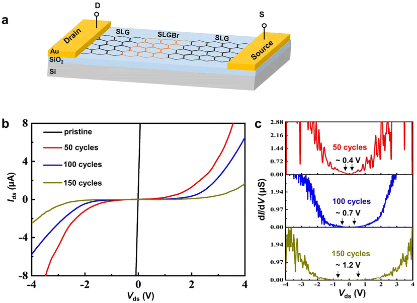 | ||
| Fig. 3 (a) The illustration of a typical SLG/SLGBr/SLG diode. (b) The Ids–Vds curves of SLG/SLGBr/SLG diodes with different degrees of bromination. (c) The corresponding differential conductance dI/dV as a function of Vds for the diodes. | ||
The differential conductance (dI/dV) as a function of Vds has previously been employed to evaluate the band gap of Gr.33–35 As shown in Fig. 3c, the potentials where dI/dV is equal to 0 are marked for the different SLG/SLGBr/SLG diodes. Thus, the rectification potential ranges are measured as 0.4 V, 0.7 V and 1.2 V, from which band gaps of 0.4 eV, 0.7 eV and 1.2 eV are estimated for SLGBr with the brominating processes of 50, 100 and 150 potential-scan cycles, respectively. Depending on the potential-scan cycles, the band gap of SLGBr is indeed determined by the degree of bromination, that can easily be characterized by the amount of sp3-C defects of SLGBr. This is well demonstrated by the linear correlation between the band gap and the ratio of ID/IG and ID’/IG shown in Fig. 4a and b.
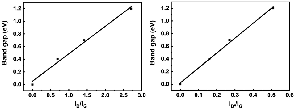 | ||
| Fig. 4 Band gap of SLG/SLGBr/SLG diodes with different degrees of bromination vs. (a) ID/IG and (b) ID′/IG, respectively. | ||
The current rectification performances are evaluated by multiple potential-step experiments, as shown in Fig. 5a. The applied potentials were set at −4.0 V, 0 V and 4.0 V with a period of 0.5 seconds. The current–time (I–t) curve shows the rapid and stable response of the current on/off switch. The stability of the SLG/SLGBr/SLG diodes was characterized, as shown in Fig. 5b with multiple cycles, Fig. 5c with different preservation times and Fig. 5d at different temperatures. The excellent electronic performances show that both the SLGBr and the SLG/SLGBr/SLG junctions have very good stability due to the covalent C–Br bond formed by the electrochemically induced brominating addition reaction. The results are different from what was reported previously by doping SLG with hydrogen, fluorine or oxygen plasma.21–23 However, the thermal stability of SLGBr is much better than these results. All the results indicate the feasibility of fabricating all-in-SLG electronic elements or circuit boards by electrochemical nanoimprint lithography in the future.36–38
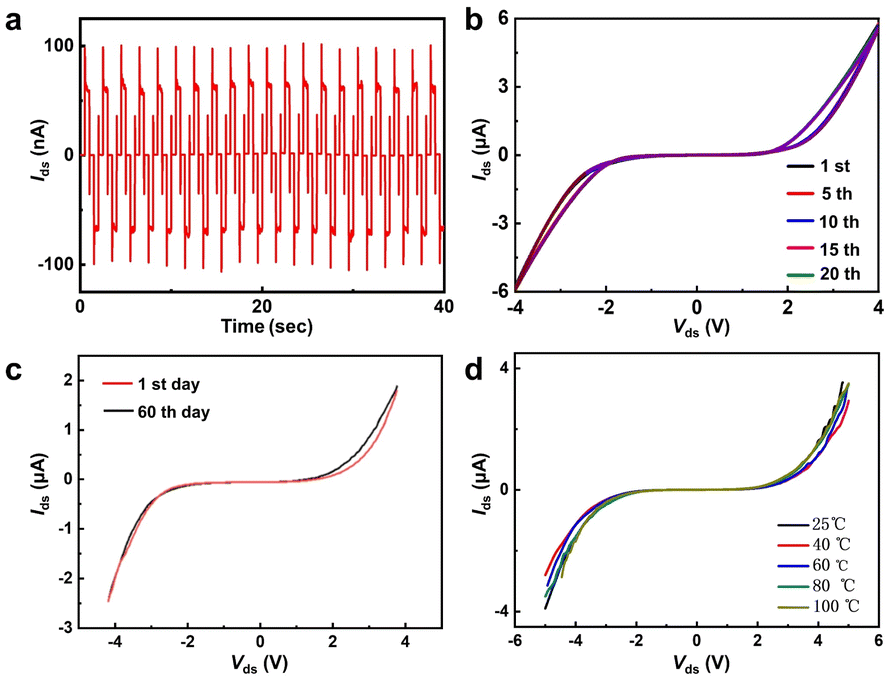 | ||
| Fig. 5 (a) The multiple potential-step response of a SLG/SLGBr/SLG diode obtained with 150 potential-scan cycles. (b) The Ids–Vds response of the diode. (c) The Ids–Vds response of the diode before and after storage for two months. (d) The Ids–Vds responses of the diode after treatment at different temperatures. | ||
Experimental
Chemicals and materials
All chemicals used in the experiments (H2SO4, KBr, (NH4)2S2O8, acetone, isopropanol) were of analytical grade, purchased from Sinopharm Group Co. Ltd. and used as received without further purification. Copper foil (25 μm, 99.8%) and poly(methylmethacrylate) (PMMA, 99.9%) for graphene preparation were purchased from Alfa Aesar Co. The photoresist (AZ5214E) was purchased from Merck Group. High-purity gases used in graphene growth (N2, CH4, Ar, 99.999%) were purchased from Linde Gas Co. High-purity hydrogen (H2, 99.999%) was produced by a hydrogen generator. All aqueous solutions were prepared with ultrapure water (18.2 MΩ cm, Milli-Q, Millipore Co.).Fabrication of the microchip with an SLG microstrip array
SLG was grown on the copper foils (2 cm by 2 cm) by CVD (FirstNano, ET2000) and then transferred to a 300 nm-thickness silicon dioxide (SiO2)-covered silicon (Si) wafer using polymethylmethacrylate (PMMA) as a transfer mediator. After that, a microchip with SLG strips (width: 700 μm, length: 1 cm) array was fabricated, as depicted in Fig. 6: first, a thin layer of AZ5214E photoresist was spin-coated on the SiO2/Si wafer supported SLG (Fig. 6a); then, the photoresist layer was patterned with laser direct-writing lithography (Microtech, LW405D) to leave spaces and, on the exposed SLG area, a 10 nm-thickness chrome (Cr) film and then a 40 nm-thickness gold (Au) film (700 μm by 500 μm) were deposited by magnetron sputtering, acting as the current terminals of the SLG diodes, and then the photoresist layer between the aligned SLG strips was removed by laser direct-writing lithography (Fig. 6b). After that, the exposed SLG areas were removed by oxygen plasma etching (Fig. 6c). Finally, the SLG microstrip array was prepared by removing the residual photoresist (Fig. 6d).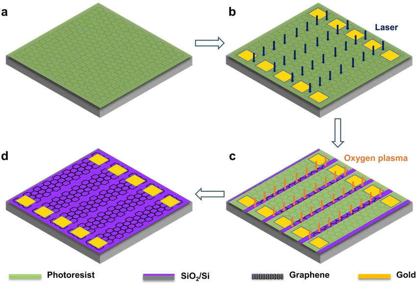 | ||
| Fig. 6 Fabrication of the microchip with an SLG microstrip array. (a) A thin layer of AZ5214E photoresist was spin-coated on SLG. (b) A gold connector was deposited on both ends of the SLG microstrip to form a good ohmic contact with the external circuit; the photoresist layers between the aligned SLG belts were then removed. (c) The exposed graphene was etched by oxygen plasma. (d) The photoresist protection layer was removed by acetone and isopropanol. | ||
Electrochemical microfabrication and electronic characterization of the SLG/SLGBr/SLG diodes
The central area of each SLG strip was brominated by a scanning electrochemical microscopy (SECM) workstation (CHI 920c, CH Instruments Inc.). As depicted in Fig. 1a, a micropipette (inner diameter: 1 mm) was employed as the electrolyte cell, inside which two platinum (Pt) wires act as the counter electrode and reference electrode. The aqueous electrolyte contained 10 mM KBr and 10 mM H2SO4. The micropipette was fixed on the SLG strip, acting as the working electrode. Cyclic voltammetry was performed to brominate SLG in the potential range [−0.5 V, 1.4 V] with a scan rate of 100 mV s−1. The band gap of SLG was tuned by controlling the number of potential-scan segments, i.e., the degree of bromination of SLG. Once the SLG/SLGBr/SLG diodes were prepared, their current rectification performances were evaluated with a Keithley 4200 SCS probe station in source–drain configuration in a clean and shielded box.Instrumental characterizations of the SLG/SLGBr/SLG diodes
Raman measurements were performed to characterize the sp3-defects of SLG on an Xplora (Horiba Jobin Yvon, France) with 532 nm laser excitation. The Raman spectra were recorded with 1200 lines per mm grating, and the laser power kept at 5 mW with an acquisition time of 2 s. X-ray photoelectron spectroscopy (XPS) data were recorded to identify the occurrence of the brominating addition reaction, i.e., the formation of C–Br bonds, on a Kratos Axis Supra instrument (Kratos Analytical, Manchester, UK) using monochromatic Al Kα radiation (1486.7 eV, 150 W) with a spot size of 400 μm. Survey spectra were acquired using an analyzer pass energy of 160 eV and 1 eV step size. Core level spectra were acquired using a pass energy of 40 eV and 0.1 eV step size. The hybrid lens mode was used in both cases. A charge neutralizer was used throughout the measurements after the samples were mounted, so that they were electrically isolated from the sample bar. Spectral calibration was done over Si at 103 eV, in order not to lose information with C 1s. The core level spectra were peak-fitted using CasaXPS software, version 2.3.18. UV-visible-NIR absorption spectroscopy (Varian, Cary 5000) was employed to characterize the light absorption properties of the SLG strips and SLG-Br patterns. Optical microscopy (Olympus, BX-60) and scanning electron microscopy (SEM, JEOL, JXA-840) were also used to characterize the morphology of the SLG strips and the SLG/SLGBr/SLG diodes.Conclusions
We demonstrated that the band gap of SLG can be opened and regulated by an electrochemically induced brominating addition reaction. The SLG bromination was assessed by characterizing the sp3-C defect contents of the crystalline structure of SLG with Raman spectroscopy, and the formation of covalent C–Br bonds with XPS experiments. The current rectification performance of the SLG/SLGBr/SLG diodes were evaluated by the I–V and I–t curves and detected under different working conditions, including multiple potential–modulation cycles, preservation time and temperature, showing excellent performance, duration and stability of current rectification. Most importantly, the band gap of SLGBr has very good correlation to the degree of bromination of SLG, which can easily be regulated by tuning the degree of bromination during the voltammetric microfabrication of the SLG/SLGBr/SLG diodes. In this work, we provide an effective way to open and regulate the band gap of SLG and make SLG a qualified semiconductor. This will provide feasibility to produce all-in-SLG electronic elements and further electronic circuits.Data availability
The authors declare that all data supporting the findings of this study are available from the corresponding author upon reasonable request.Author contributions
L. Zeng and W. Song contributed equally. L. Zeng, Q. He, Y.-f. Wu, L. Han: electrochemical experiments and instrumental characterizations; L. Zeng, W. Song, Y. Cao: microfabrication and electronic characterizations; L. Han, X. Jin, J. Cheng: theoretical discussions; C. Lagrost, Y. Leroux, P. Hapiot: XPS analysis; D. Zhan: originated, designed and organized the work and wrote the manuscript. All the authors participated in the discussions and preparation of the manuscript.Conflicts of interest
There are no conflicts to declare.Acknowledgements
The financial support from the National Natural Science Foundation of China (21827802, 22202166, 22132003, 22021001) and the 111 Project (B08027, B17027) are appreciated as well as the Chinese-French IRP CNRS NanoBioCatEchem International Laboratory.Notes and references
- K. Kim, J. Y. Choi, T. Kim, S. H. Cho and H. J. Chung, Nature, 2011, 479, 338–344 CrossRef CAS PubMed.
- A. Kaplan, Z. Yuan, J. D. Benck, A. G. Rajan, X. S. Chu, Q. H. Wang and M. S. Strano, Chem. Soc. Rev., 2017, 46, 4530–4571 RSC.
- L. Wang, I. Meric, P. Y. Huang, Q. Gao, Y. Gao, H. Tran, T. Taniguchi, K. Watanabe, L. M. Campos, D. A. Muller, J. Guo, P. Kim, J. Hone, K. L. Shepard and C. R. Dean, Science, 2013, 342, 614–617 CrossRef CAS PubMed.
- Q. He, L. Zeng, L. Han, J. Peng, M. M. Sartin, Y.-Z. Tan, D. Zhan and Z.-Q. Tian, Sci. China: Chem., 2022, 65, 318–321 CrossRef CAS.
- M. I. Katsnelson, K. S. Novoselov and A. K. Geim, Nat. Phys., 2006, 2, 620–625 Search PubMed.
- A. C. Neto, F. Guinea, N. M. Peres, K. S. Novoselov and A. K. Geim, Rev. Mod. Phys., 2009, 81, 109 CrossRef.
- K. S. Novoselov, V. I. Fal'ko, L. Colombo, P. R. Gellert, M. G. Schwab and K. Kim, Nature, 2012, 490, 192–200 CrossRef CAS PubMed.
- M. C. Lemme, T. J. Echtermeyer, M. Baus and H. Kurz, IEEE Electron Device Lett., 2007, 28, 282–284 CAS.
- K. Kim, J.-Y. Choi, T. Kim, S.-H. Cho and H.-J. Chung, Nature, 2011, 479, 338–344 CrossRef CAS PubMed.
- D. Reddy, L. F. Register, G. D. Carpenter and S. K. Banerjee, J. Phys. D: Appl. Phys., 2011, 44, 313001 CrossRef.
- X. Xu, C. Liu, Z. Sun, T. Cao, Z. Zhang, E. Wang, Z. Liu and K. Liu, Chem. Soc. Rev., 2018, 47, 3059–3099 RSC.
- Y. Zhang, T.-T. Tang, C. Girit, Z. Hao, M. C. Martin, A. Zettl, M. F. Crommie, Y. R. Shen and F. Wang, Nature, 2009, 459, 820–823 CrossRef CAS PubMed.
- S. Y. Zhou, G. H. Gweon, A. V. Fedorov, P. N. First, W. A. De Heer, D. H. Lee, F. Guinea, A. H. Castro Neto and A. Lanzara, Nat. Mater., 2007, 6, 916 CrossRef CAS.
- F. Schwierz, J. Pezoldt and R. Granzner, Nanoscale, 2015, 7, 8261–8283 RSC.
- P. Rakyta, A. Kormanyos and J. Cserti, Phys. Rev. B: Condens. Matter Mater. Phys., 2011, 83, 155439 CrossRef.
- X. Xu, W. Yao, D. Xiao and T. F. Heinz, Nat. Phys., 2014, 10, 343–350 Search PubMed.
- Z. H. Ni, T. Yu, Y. H. Lu, Y. Y. Wang, Y. P. Feng and Z. X. Shen, ACS Nano, 2008, 2, 2301–2305 CrossRef CAS PubMed.
- M. Papagno, S. Rusponi, P. M. Sheverdyaeva, S. Vlaic, M. Etzkorn, D. Pacilé, P. Moras, C. Carbone and H. Brune, ACS Nano, 2012, 6, 199–204 CrossRef CAS PubMed.
- Z. Jin, J. Yao, C. Kittrell and J. M. Tour, ACS Nano, 2011, 5, 4112–4117 CrossRef CAS PubMed.
- S. Zhang, S. Lin, X. Li, X. Liu, H. Wu, W. Xu, P. Wang, Z. Wu, H. Zhong and Z. Xu, Nanoscale, 2016, 8, 226–232 RSC.
- R. Balog, B. Jørgensen, L. Nilsson, M. Andersen, E. Rienks, M. Bianchi, M. Fanetti, E. Lægsgaard, A. Baraldi and S. Lizzit, Nat. Mater., 2010, 9, 315–319 CrossRef CAS PubMed.
- R. Zbořil, F. Karlický, A. B. Bourlinos, T. A. Steriotis, A. K. Stubos, V. Georgakilas, K. Šafářová, D. Jančík, C. Trapalis and M. Otyepka, Small, 2010, 6, 2885–2891 CrossRef PubMed.
- A. Nourbakhsh, M. Cantoro, T. Vosch, G. Pourtois, F. Clemente, M. H. van der Veen, J. Hofkens, M. M. Heyns, S. De Gendt and B. F. Sels, Nanotechnology, 2010, 21, 435203 CrossRef PubMed.
- J. O. Sofo, A. S. Chaudhari and G. D. Barber, Phys. Rev. B, 2007, 75, 153401 CrossRef.
- D. C. Elias, R. R. Nair, T. Mohiuddin, S. Morozov, P. Blake, M. Halsall, A. C. Ferrari, D. Boukhvalov, M. Katsnelson and A. Geim, Science, 2009, 323, 610–613 CrossRef CAS PubMed.
- D. Chen, Z. Lin, M. M. Sartin, T.-X. Huang, J. Liu, Q. Zhang, L. Han, J.-F. Li, Z.-Q. Tian and D. Zhan, J. Am. Chem. Soc., 2020, 142, 6516–6520 CrossRef CAS PubMed.
- J.-H. Zhong, J. Zhang, X. Jin, J.-Y. Liu, Q. Li, M.-H. Li, W. Cai, D.-Y. Wu, D. Zhan and B. Ren, J. Am. Chem. Soc., 2014, 136, 16609–16617 CrossRef CAS PubMed.
- M. S. Dresselhaus, A. Jorio, A. S. Filho and R. Saito, Philos. Transact. A Math. Phys. Eng., 2010, 368, 5355–5377 CAS.
- A. C. Ferrari and D. M. Basko, Nat. Nanotechnol., 2013, 8, 235–246 CrossRef CAS PubMed.
- A. Eckmann, A. Felten, A. Mishchenko, L. Britnell, R. Krupke, K. S. Novoselov and C. Casiraghi, Nano Lett., 2012, 12, 3925–3930 CrossRef CAS PubMed.
- O. Jankovský, P. Šimek, K. Klimova, D. Sedmidubský, S. Matějková, M. Pumera and Z. Sofer, Nanoscale, 2014, 6, 6065–6074 RSC.
- L. G. Bulusheva, A. V. Okotrub, E. Flahaut, I. P. Asanov, P. N. Gevko, V. Koroteev, Y. V. Fedoseeva, A. Yaya and C. P. Ewels, Chem. Mater., 2012, 24, 2708–2715 CrossRef CAS.
- T. Shimizu, J. Haruyama, D. Marcano, D. Kosinkin, J. Tour, K. Hirose and K. Suenaga, Nat. Nanotechnol., 2011, 6, 45–50 CrossRef CAS PubMed.
- M. Y. Han, J. C. Brant and P. Kim, Phys. Rev. Lett., 2010, 104, 056801 CrossRef PubMed.
- H. Chen, X.-L. Zhang, Y.-Y. Zhang, D. Wang, D.-L. Bao, Y. Que, W. Xiao, S. Du, M. Ouyang and S. T. Pantelides, Science, 2019, 365, 1036–1040 CrossRef CAS PubMed.
- D. Zhan, L. Han, J. Zhang, Q. He, Z.-W. Tian and Z.-Q. Tian, Chem. Soc. Rev., 2017, 46, 1526–1544 RSC.
- J. Zhang, L. Zhang, W. Wang, L. Han, J.-C. Jia, Z.-W. Tian, Z.-Q. Tian and D. Zhan, Chem. Sci., 2017, 8, 2407–2412 RSC.
- L. Han, Y. Jia, Y. Cao, Z. Hu, X. Zhao, S. Guo, Y. Yan, Z. Tian and D. Zhan, Sci. China: Chem., 2018, 61, 715–724 CrossRef CAS.
| This journal is © The Royal Society of Chemistry 2023 |