
 Open Access Article
 This Open Access Article is licensed under a Creative Commons Attribution-Non Commercial 3.0 Unported Licence
Low-frequency noise in nanowires
Daniel M.
Fleetwood

Department of Electrical and Computer Engineering, Vanderbilt University, Nashville, TN 37235, USA. E-mail: dan.fleetwood@vanderbilt.edu
First published on 6th July 2023
Abstract
40 years of research on low-frequency (LF) noise and random-telegraph noise (RTN) in metallic and semiconducting nanowires (NWs) demonstrate the importance of defects and impurities to each system. The fluctuating interference of electrons in the local environment of a mobile bulk defect or impurity can lead to LF noise, RTN, and device-to-device variations in metallic and semiconducting NWs. Scattering centers leading to mobility fluctuations in semiconducting NWs include random dopant atoms and bulk defect clusters. Effective energy distributions for the relevant defects and impurities can be obtained from noise versus temperature measurements in conjunction with the Dutta–Horn model of LF noise for both metallic and semiconducting NWs. In semiconducting NWs configured as metal-oxide-semiconductor field-effect transistors, fluctuations in carrier number due to charge exchange with border traps, such as oxygen vacancies and/or their complexes with hydrogen in adjacent or surrounding dielectrics, often dominate or add to bulk noise sources.
 Daniel M. Fleetwood | Dan Fleetwood received his Ph.D. from Purdue University in 1984. He joined Sandia National Laboratories in 1984 and was named a Distinguished Member of Technical Staff in 1990. Dan joined Vanderbilt University as a Professor of Electrical Engineering in 1999. From 2003–2020 he chaired Vanderbilt's EECS Department; since 2009 he has been appointed Olin H. Landreth Chair in Engineering. He received the 2009 IEEE Nuclear and Plasma Sciences Merit Award, and is a Fellow of IEEE, AAAS, and the American Physical Society. His research interests include radiation effects on microelectronics, low-frequency noise, and defects in microelectronic materials and devices. |
I. Introduction
Size and scale matter. The transitions from classical to quantum regimes and bulk to surface-dominated responses have been intense areas of study over the last century. In recent decades, metallic and semiconducting nanowires (NWs) have enabled investigations of a wide range of phenomena including Anderson localization, electron–electron interactions, and quantum-mechanical decoherence;1–23 magnetism, including Aharonov–Bohm oscillations and the Kondo effect;11,18,23–39 superconductivity, macroscopic quantum tunnelling, and Majorana bound states;39–50 and low-frequency noise, random-telegraph noise, and universal conductance fluctuations.51–77When pioneering experimental studies of localization and electron–electron interactions were performed on metallic NWs fabricated via substrate step methods in 1979–1982,5–9 the semiconductor industry was transitioning from the micron to the submicron scale.78–81 For several decades, typical metal-oxide-semiconductor field-effect transistor (MOSFET) channel dimensions were several orders of magnitude larger than mesoscale and nanoscale NWs.5–9,12,20 As microelectronic fabrication techniques advanced, NW fabrication techniques evolved from substrate step and templating methods to state-of-the-art lithography capable of producing nanostructures in volume and integrating semiconductor NWs into architectures that facilitate fabrication and measurement.5–9,12,20,71–77,81,82
This paper reviews the evolution of low-frequency (LF) and random-telegraph noise (RTN) in metallic and semiconducting NWs over the last ∼40 years. Defects and impurities are critical to the noise of each system. Metal NWs are passive devices; semiconducting NWs typically are built as active devices. The noise of semiconducting NWs is especially important to future analog integrated circuits (ICs), since LF noise and RTN often limit their accuracy and precision.55,60,66,81
This review is organized as follows. Section II presents an overview of LF noise and RTN in metals and semiconductor devices. The Dutta–Horn model of thermally-activated 1/f noise, where f is the frequency, and the number fluctuation model of LF noise in MOSFETs are emphasized.55,66,73,76 LF noise and RTN of metallic NWs are discussed in Section III; representative results for semiconducting NWs with Si and III–V semiconductor channels are shown in Section IV. Bulk noise persists over large volumes in metallic NWs.51,71,83 Fluctuations due to single defects become increasingly common in highly scaled devices of each type.15,53–58,66,74–77,84–90 These results illustrate the diversity of mechanisms that can lead to conductivity fluctuations in metallic and semiconducting NWs.
II. Overview of low-frequency noise
| SVt = 4kTR. | (1) |
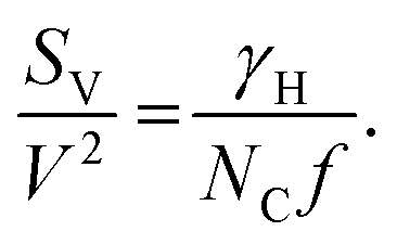 | (2) |
Here γH is a dimensionless figure of merit proportional to noise magnitude and NC is the number of channel carriers. For a metal, it is usually assumed that NC ≈ NA, where NA is the number of atoms.51,55,95
Fig. 1 shows a room-temperature LF noise spectrum for a first-generation sputtered-platinum NW fabricated using substrate step lithography via the process sequence shown schematically in Fig. 2.5,7,8,51 NWs fabricated via substrate step lithography are poly-crystalline, with grain sizes less than wire diameters.5,7–9,16,20,51–54 The noise magnitude of the NW in Fig. 1 increases as 1/f![[thin space (1/6-em)]](https://www.rsc.org/images/entities/char_2009.gif) 1.15 over nearly five decades in frequency. The Hooge parameter at f = 1 Hz is γH ≅ 3 × 10⁻⁴, a typical value for sputtered Pt wires and thin films.51,71,96,97 The 1/N ≈ 1/NA dependence of the noise magnitude in eqn (2) presumes a bulk origin for the fluctuations.
1.15 over nearly five decades in frequency. The Hooge parameter at f = 1 Hz is γH ≅ 3 × 10⁻⁴, a typical value for sputtered Pt wires and thin films.51,71,96,97 The 1/N ≈ 1/NA dependence of the noise magnitude in eqn (2) presumes a bulk origin for the fluctuations.
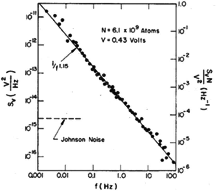 | ||
| Fig. 1 Excess voltage-noise power spectral density SV as a function of frequency f for a Pt nanowire (NW) fabricated via substrate step lithography. The Johnson (thermal) noise background has been subtracted. The size and voltage normalized noise, SVN/V,2 is shown on the right-h and y-axis, with N = NA. Reproduced from ref. 51 with permission. Copyright 1983 The American Physical Society. | ||
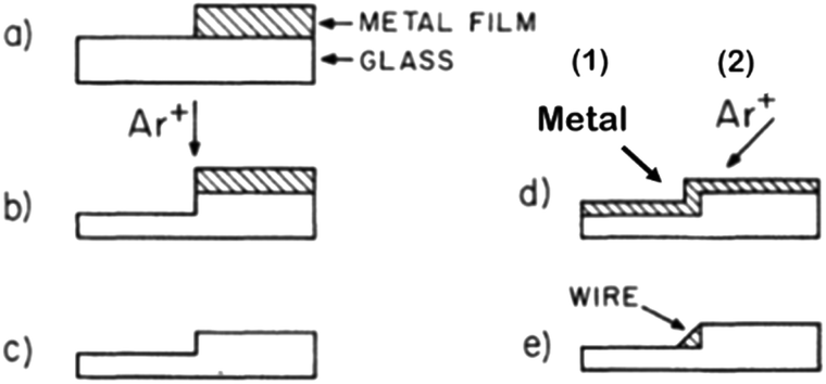 | ||
| Fig. 2 Schematic illustration of substrate step lithography. (a) Metal is deposited onto the unmasked portion of a glass slide. (b) The masking metal is removed via argon ion milling, leaving behind (c) a step in the substrate. (d) Step 1: metal is deposited at an angle favoring step filling. Step 2: without breaking vacuum, argon ion milling removes all metal except that shadowed by the step, leaving (e) a nanowire. Adapted from ref. 5 with permission. Copyright 1979 The American Physical Society. | ||
Several key experiments in the late 1970s through mid-1980s demonstrate the crucial roles of defects and impurities in LF noise in metals.52,55,66,83,95,98–103 One defect with a single characteristic scattering or transition time τ leads to RTN with a Lorentzian spectrum that falls off as 1/f2 at frequencies above 1/τ and is constant at frequencies below 1/τ.55,62,66,95,104–106 An example is shown for a ZnO NW in Section II.B. If instead the noise results from multiple defects having a distribution of characteristic times D(τ), and if D(τ) ∼ 1/τ for times τ1 < τ < τ2, then the integrated noise,
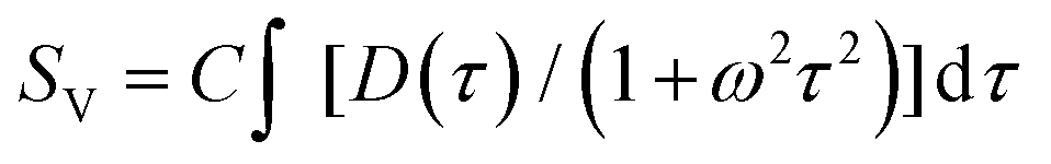 | (3) |
is proportional to ∼1/f for 1/τ2 < f < 1/τ1.55,66,95,104,105 Here ω = 2πf and C is a frequency-independent parameter that is proportional to the noise magnitude. If the noise results from a random, thermally activated process, as is often the case,52,66,95,104,107 then
| τ = τ0eE/kT, | (4) |
ln(τ2/τ0) ≤ E ≤ kTln(τ1/τ0), the condition that D(τ) is proportional to ∼1/τ is satisfied, and 1/f noise is observed.55,95,104,105 This follows directly from the solution of eqn (3), with an exchange of variables (τ, E).104,105
Dutta and Horn extended this approach to show that, if the noise is caused by a random thermally activated process that is not approximately constant in energy, but changes in the distribution occur slowly with respect to kT, the frequency and temperature dependences of the noise are correlated via:52,55,66,95
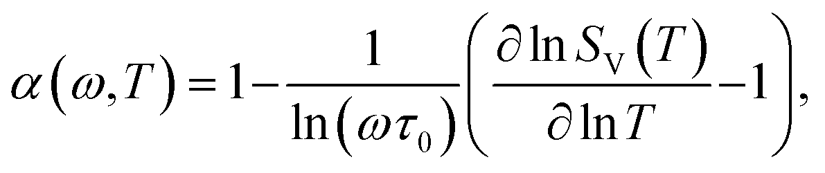 | (5) |
ln SV/∂lnf. When the measured frequency and temperature dependences of the noise follow eqn (5), the effective defect-energy distribution D(E0) can be estimated via:52,55,66,73,95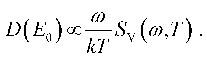 | (6) |
The energy that corresponds to a given temperature in a plot of SVvs. T can be estimated to first order via:55,66,95,107
| E0 ≈ −kTln (ωτ0). | (7) |
Fig. 3 shows normalized noise as a function of temperature for Pt NWs similar to those in Fig. 1.96 The energy scale inferred from eqn (7) is shown on the upper x-axis, assuming τ0 ≈ 10−14 s, a typical value for metals.55,66,95 The noise of the two wires differs by less than a factor of 2 up to ∼300 K, with more significant differences at higher temperatures and energies.96 Additional studies of the temperature dependence of the noise of metallic NWs are shown in Section III.
 | ||
| Fig. 3 Normalized noise magnitude vs. temperature for two Pt NWs. The energy E0 that corresponds to the temperature T viaeqn (7) is shown on the upper x-axis, assuming τ0 ≈ 10−14 Hz. Adapted from ref. 96 with permission. Copyright 1987 American Institute of Physics. | ||
For thin metal films and NWs, variations in scattering rates caused by defect and/or impurity motion and/or the reconfiguration of bulk defect complexes often are dominant sources of 1/f noise.52,55,66,86,95 In most cases, the noise is due to the fluctuating interference of electrons in the local environment of a moving defect or impurity.55,86 At low temperatures, the noise may also be due to universal conductance fluctuations (UCF), in which the motion of one strong scattering center leads to conductance fluctuations of order q2/h, where q is the magnitude of the electron charge and h is Planck's constant.15,85 Examples are shown in Section III.
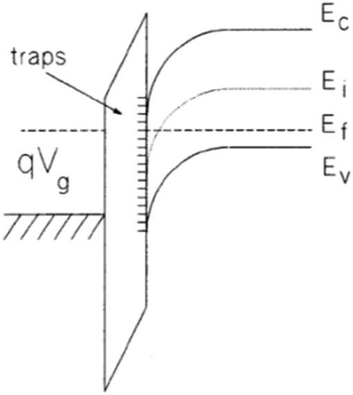 | ||
| Fig. 4 Schematic band diagram for an nMOS transistor biased in inversion. Reproduced from ref. 112 with permission. Copyright 1991 Institute of Electrical and Electronics Engineers. | ||
When contact noise is controlled effectively during device fabrication, near-interfacial oxide traps (border traps) can lead to LF noise and RTN in MOSFETs.56,66,73,74,76,77,90,107–124 In the Si MOS literature, particularly before the early 1990s, these defects are often erroneously called interface traps (or states).113,116 This term should be applied only to defects at the interface that are in rapid communication with the channel, typically on ∼μs time scales for Si MOS devices.66,73,90,107,113,116–119,125,126 In contrast, charge exchange times for border traps of relevance to LF noise measurements typically are ms to s (or longer) in Si MOS devices.113,116,118,119,125 Note that, for wide band-gap (WBG) semiconductors, e.g., SiC and GaN, separating effects of interface and border traps on device response and/or LF noise is more challenging than for Si, Ge, GaAs, and other narrow gap semiconductors, due to the significant overlap between time constants for deep interface traps and border traps in WBG devices.55,66,113,116,118,123,126,127
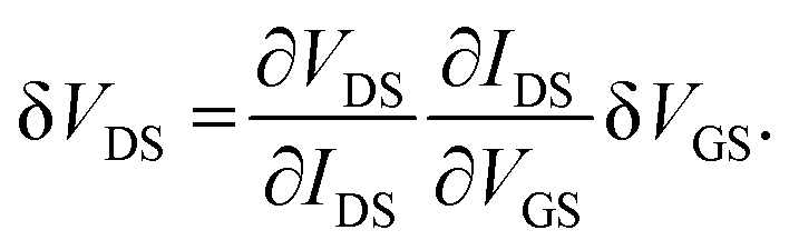
Fig. 4 schematically illustrates an nMOS transistor biased in inversion. For constant drain current IDS and gate bias VGS in the linear region of MOS operation, fluctuations in trapped charge density and occupancy δQt have an effect that is equivalent to fluctuations in gate voltage δVGS:73,108,112
 | (8) |
 | (9) |
 | (10) |
 | (11) |
Again, when individual defects dominate device response, RTN and Lorentzian power spectra are observed,55,56,59,62,66,88,95,104–106 as shown for a ZnO NW in Fig. 5. RTN is shown in the inset; the resulting power spectrum has a 1/f2 corner frequency of ∼18 Hz for a NW measured in vacuum at a temperature of 4.2 K.62
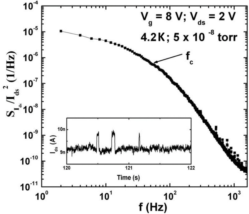 | ||
| Fig. 5 Lorentzian noise power spectrum for a ZnO NW exhibiting random telegraph noise, RTN, at a temperature of 4.2 K. The corner frequency fc is ∼18 Hz. The inset plots current vs. time. Reproduced from ref. 62 with permission. Copyright 2007 American Institute of Physics. | ||
For RTN due to one or a few prominent border traps, the expected change in drain current IDS in the linear mode of device operation in a simple number-fluctuation model (neglecting mobility fluctuations) is:76,110,111
 | (12) |
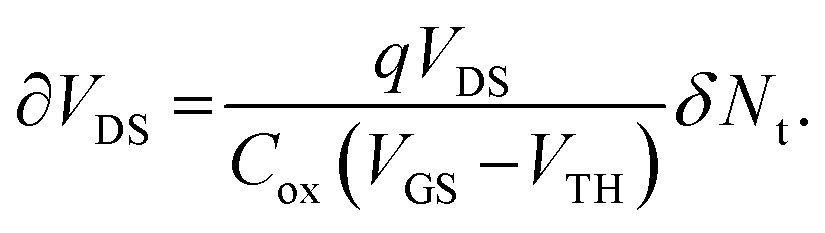
When more than a few defects are active on the time scales of the measurements, 1/f noise is observed.55,66,73,84,112 The excess drain-voltage noise power spectral density SVd can be related viaeqn (10) to fluctuations in the trapped charge density in the near-interfacial dielectric:73,108,112
 | (13) |
Thus, in the number fluctuation model of low frequency noise, SVd is proportional to 1/NC2. This contrasts with eqn (2), in which SVd is proportional to 1/NC.76,93,94,110,111 The ability to modify NC within a given device for MOS transistors provides information on the nature of the fluctuations not often available for metals.51,55,76,93–95,110,111 Indeed, measurements of LF noise vs. current and/or voltage, and thus NC, are often performed on MOS devices to attempt to differentiate bulk noise due to fluctuations in carrier scattering rates from surface noise due to fluctuations in occupancy of border traps.93,94,111,115 However, these tests are open to multiple interpretations, as discussed below, so additional information typically is required to determine whether bulk or surface noise dominates the response of a particular device.66,73,128
For simplicity in calculation, it is commonly assumed that the exchange of charge between the device channel and border traps occurs via tunneling, and that defects are distributed approximately uniformly in space within the gate insulator and in energy within the Si band gap.73,108–115 With these simplifying assumptions, fluctuations in the density of traps Nt lead to a power-spectral density SNt:73,108,112
 | (14) |
In this case Nt = DBT(Ef) is the effective number of border traps per unit energy and area at the Fermi level Ef, and τ1 and τ2 are minimum and maximum tunneling times. Combining eqn (13) and (14) yields a first-order expression that relates SVd to DBT(Ef) in the linear mode of transistor response:73,108,112
 | (15) |
Hence, when MOS 1/f noise is due primarily to border traps, DBT is an effective measure of relative noise magnitude.66,93,113–115,117,118
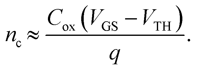
In a first-order number fluctuation model, SId/Id2 is proportional to (gm/Id)2 in both linear and saturation modes of transistor operation.111,115,129 Electric fields are stronger and less uniform in saturation than in the linear mode. Thus, deviations from nominal response often are observed as voltage and current increase in a MOS transistor, particularly when surface roughness scattering, mobility fluctuations, spatial variations in trap density, and/or areal variations in trap density are significant.66,73,111,115
Although good agreement between eqn (15) and complementary methods to estimate border-trap densities in MOSFETs is often observed,66,90,113,117,118 caution must be used when interpreting results because (1) thermally activated charge exchange is much more common in MOS devices than purely quantum-mechanical tunneling exchange,66,76,90,130 (2) border-trap energy distributions are often non-uniform in space and/or energy,66,90,107,128,131–134 and (3) bulk defects and impurities in the device channel also contribute to 1/f noise and/or RTN in some MOS devices.73,74,76,77,110,111,130,135,136
The Hooge model is often applied to semiconductor devices in an effort to analyze noise due to mobility fluctuations.55,66,93–95,111,114,137 However, the Hooge model as formulated in 1969 and updated in 1978 attributes the noise to lattice scattering.93,94,137 The lack of a theoretical foundation, internal inconsistencies, and crucial roles for defects and impurities in the 1/f noise of microelectronic devices and materials argue persuasively against Hooge mobility fluctuations as the origin of noise in metals or semiconductor devices.55,66,76,86,95,128 As a result, the Hooge parameter as defined in eqn (2) is not as useful in comparisons of the relative noise levels of semiconducting devices as it is for metals.55,66,93–95,114
Correlated mobility fluctuation (CMF) models are often used to analyze LF noise in semiconductor devices.76,110,111,115,135,136 In the CMF model, simultaneous changes in charge state and strength of scattering of channel carriers by border traps are inferred to lead to enhanced LF noise over simple number fluctuation predictions viaeqn (15). In the CMF model of Hung, et al., for example, the input-referred noise power spectral density, SVg, is given by:110,111,115,135,136
 | (16) |
It can be challenging to interpret eqn (16) physically. As noted above, charge exchange between the channel and border traps is rarely due to pure tunneling. Moreover, when this charge exchange occurs at capture and emission rates accessible to typical LF noise measurements, the Coulomb interaction between channel carriers and border traps is often too weak to lead to the enhanced scattering in eqn (16), compared with eqn (15), and/or increased RTN, compared with eqn (12), as discussed in Section IV.76,110,111,115,130,135 It is more likely that the enhanced 1/f noise or RTN in these cases is caused by (1) fluctuations in scattering rates caused by random dopants, (2) changes in charge state or configuration of bulk defect clusters in the device channel, and/or (3) fluctuating concentrations of interface traps caused by hydrogen-mediated interface-trap activation and passivation.76,77,138–144 These are fruitful areas for future study.
Values of DBT often depend strongly on temperature, consistent with the critical role that thermally activated processes play in the LF noise of MOS and other semiconductor devices. Much work over the last ∼40 years has demonstrated that the temperature dependence of the noise of semiconductor devices is often described well by the Dutta–Horn model of 1/f noise.66,73,90,95,107,132–134,145–150Fig. 6 shows an example of the degree of agreement that is often observed, in this case for a SiGe pMOSFET.133
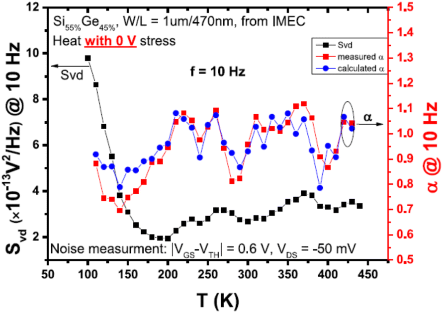 | ||
| Fig. 6 Noise magnitude (left y-axis) and measured and predicted values of α = −∂lnSV/∂lnf vs. temperature (right y-axis) for a SiGe pMOSFET with SiO2/HfO2 gate dielectric. Predicted α values are derived from the SVdvs. T curve measured before bias-temperature stress, using eqn (5) of the text. Reproduced from ref. 133 with permission. Copyright 2016 Institute of Electrical and Electronics Engineers. | ||
Comparative studies of LF noise, radiation response, and bias-temperature instabilities (e.g., Fig. 7 and 8), often supported by first principles calculations, show that O vacancies and/or complexes with hydrogen can lead to LF noise and RTN in MOSFETs with SiO2 or high-K gate dielectrics in a variety of semiconductor technologies and transistor architectures.66,73,74,90,107,109,112–114,120,122,123,132–134,145,150–153 For nMOSFETs, O vacancies in the strained region of the MOS gate oxide near the channel interface are close enough in energy to the Fermi level to contribute to 1/f noise, as illustrated in Fig. 7(a).66,73,107,133,134 Inferred defect-energy distributions for FinFETs with high-K gate dielectrics are shown in Fig. 7(b) before and after devices were subjected to bias-temperature stress and then irradiated to 2 Mrad(SiO2).154 The increase in LF noise for these and similar devices correlates strongly with O vacancy densities.109,112,114,131,154–156 For pMOS transistors, density-functional calculations suggest that LF noise and RTN are due to O vacancies complexed with hydrogen, e.g., in a hydrogen bridge configuration, as in Fig. 8(a), or hydroxyl E′ configuration, as in Fig. 8(b).73,90,157,158
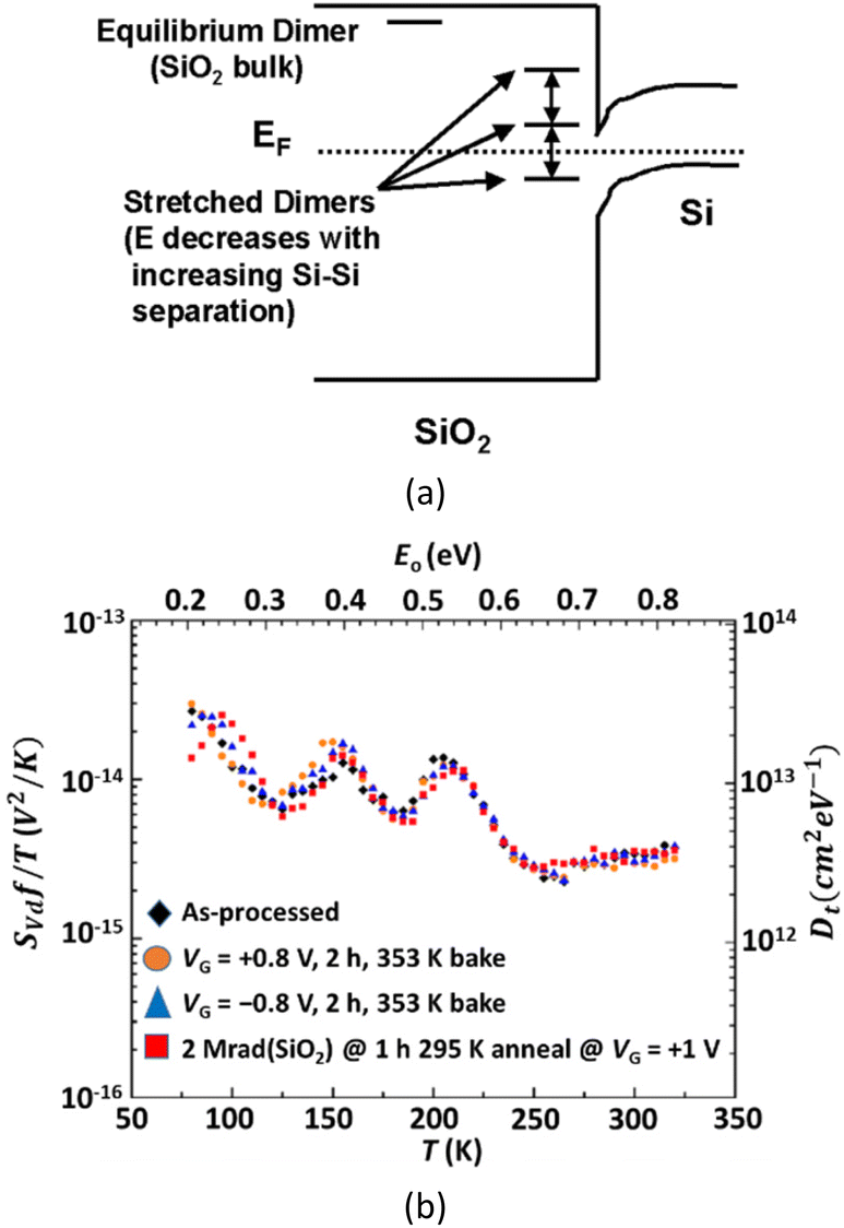 | ||
| Fig. 7 (a) Schematic diagram of dimer (unrelaxed) O vacancy energy levels in bulk and near-interfacial SiO2. Band narrowing and near-interfacial strain reduce O vacancy energies, facilitating electron capture. Electron capture relieves strain, increasing the energy, and favoring emission. Reproduced from ref. 107 with permission. Copyright 107 Institute of Electrical and Electronics Engineers. (b) Normalized 1/f noise (left y-axis) and effective border-trap density from eqn (15) (right y-axis) vs. temperature for nMOS transistors with SiO2/HfO2 gate dielectrics before and after bias-temperature stress at 353 K and 10 keV X-ray irradiation to 2 Mrad(SiO2). The energy scale on the upper x-axis is from eqn (7). Reproduced from ref. 154 with permission. Copyright 2023 Institute of Electrical and Electronics Engineers. | ||
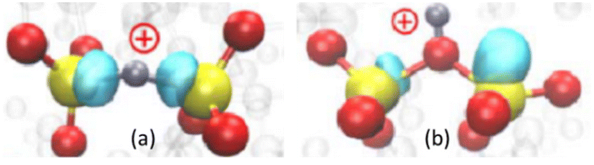 | ||
| Fig. 8 Oxygen vacancy complexes with hydrogen that are hole traps during negative-bias-temperature stress, and border traps leading to LF noise and RTN in pMOS transistors: (a) hydrogen bridge – when charged, the central hydrogen atom (small silver ball) is bonded to both Si atoms (large yellow balls), and (b) hydroxyl E′ center – when charged, a bridging O atom (medium red ball) attaches to a H atom. Reproduced from ref. 157 with permission. Copyright 2014 Institute of Electrical and Electronics Engineers. | ||
The LF noise of MOS devices with 2D materials (e.g., graphene, MoS2, BP) as channels typically is dominated by border traps with defect energy distributions similar to those in Fig. 7(b). However, traps at the 2D material surface can introduce sources of scattering-induced noise, RTN, instability, and/or part-to-part variations that can be much larger than observed in Si MOS transistors.73,121,134,158–165 Finally, carbon nanotube transistors (CNTs) can show a wide range of responses, including giant LF noise if surfaces are unpassivated or if mesh percolation significantly affects transport, border-trap related noise due to charge exchange between the CNT and adjacent oxides, and/or bulk LF noise.166–173
Knowing the microstructures of the defects that lead to LF noise and RTN enables process improvements to device response. In older technologies, limiting post-gate-oxidation annealing temperature to ∼875 °C to avoid oxygen out-diffusion from SiO2 and minimizing hydrogen to reduce interface-trap formation can lead to reduced LF noise and enhanced radiation tolerance.66,73,76,107,109,112,114,132,174,175 In newer, highly scaled technologies, defect-passivation treatments such as high-pressure annealing in hydrogen or deuterium have been effective in reducing LF noise and RTN.176–179
III. Metallic nanowires
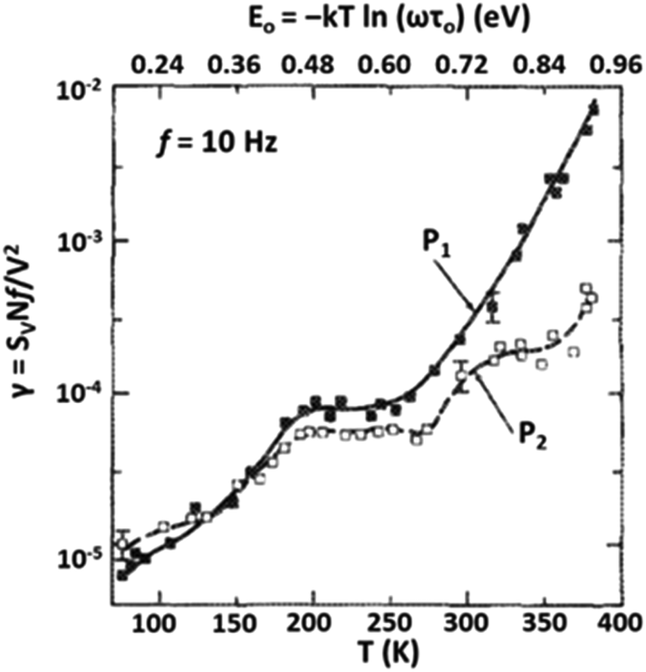
As thin-film and NW dimensions shrink, volume vs. surface scaling becomes an increasingly significant issue. However, Fig. 9 shows that, for more than six orders of magnitude in volume, an approximate ∼1/NA dependence is observed for the noise of Pt thin films and NWs.51,71 Hence, bulk fluctuations dominate the LF noise.51 This result was confirmed and extended by Zimmerman, et al.,83 for Cr films with thicknesses from 8–260 nm.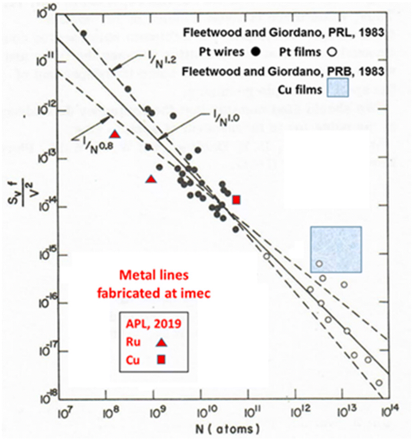 | ||
| Fig. 9 S V N/V2 at 295 K and f = 10 Hz for Pt NWs fabricated by substrate step lithography (solid black circles); mechanically scribed, sputtered Pt films (open circles); and mechanically scribed, thermally evaporated Cu films (large, blue box). Lines are proportional to 1/N(1.0±0.2). Results are compared with Ru (length L = 10 μm and 50 μm; red triangles) and Cu resistors fabricated at imec (small red box). Adapted from ref. 71 with permission. Copyright 2019 American Institute of Physics. | ||
One naturally may wonder how the noise of structures prepared by substrate step lithography and mechanical scribing in Fig. 1, 3, and 7 compares with that of devices prepared via state-of-the-art lithography. To address this point, Fig. 9 also includes results for Ru (a Pt group metal) and Cu metal lines fabricated by imec in a modern CMOS fabrication facility71 and early 1980s results for mechanically scribed Cu metal films.97 Noise magnitudes are remarkably similar for Pt NWs and Ru resistors of similar dimensions, and for scribed and patterned Cu resistors when scaled for differences in volume. The relatively modest decreases in normalized noise for imec-fabricated Ru and Cu resistors are due simply to the reduced concentrations of defects and impurities in metal lines fabricated via modern lithography than in the sputtered Pt NWs and Pt and Cu films fabricated via the first-generation techniques of Fig. 1–3.71
Giordano discovered in 1980 that as-processed, highly disordered AuPd films showed larger increases in resistance at low temperatures as a result of enhanced carrier localization and/or electron–electron interactions than films of lower resistivity and reduced disorder; these results are shown in Fig. 10.7 This finding inspired a later experiment in which a series of systematic annealing treatments on disordered AuPd NWs were performed to test the degree to which eqn (5) is satisfied.52 The results of this study are summarized in Fig. 11. Remarkably close agreement is observed between the experimental results and the predictions of eqn (5) through three measurement and annealing cycles. In Fig. 11(a) the slope of the SVvs. T curve is maximum between ∼200 K and ∼300 K in an as-processed AuPd NW. This corresponds to the maximum value of α = −∂lnSV/∂lnf in Fig. 11(b), consistent with eqn (5). When the resistivity of the NW and the noise magnitude are reduced in Fig. 11(a) as a result of in situ heating (curves A and B) or baking in an external oven (between curves B and C), changes in the frequency dependence of the noise again closely follow predictions based on eqn (5). These results clearly show the validity and utility of the Dutta–Horn model of 1/f noise.52,55,66,73,95
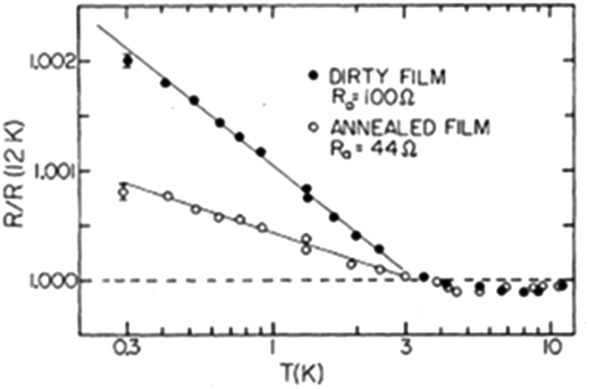 | ||
| Fig. 10 Relative resistance vs. temperature for an as-processed, sputtered AuPd thin film (“dirty”) with sheet resistance of 100 Ω □−1 and an otherwise identical film annealed for 24 h in Ar at 300 °C with sheet resistance of 44 Ω □−1. Lines are best fits to the data. Reproduced from ref. 7 with permission. Copyright 1980 The American Physical Society. | ||
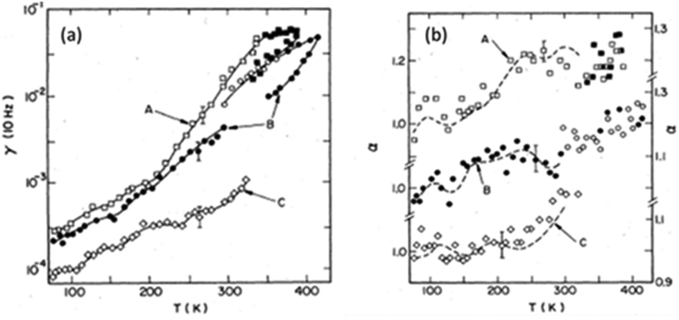 | ||
| Fig. 11 (a) γ = γH ≡ SVNf/V2 at f = 10 Hz and (b) α = −∂lnSV/∂lnf as functions of temperature and sequential annealing for sputtered AuPd NWs. (a) Open squares (curve A) show the noise of an as-processed sample with resistivity ρ(295 K) = 180 ± 20 μΩ cm. Solid squares show noise measurements while the sample is annealing in situ. Open and solid circles [curve B, ρ(295 K) = 145 ± 16 μΩ cm] show the noise during the second series of measurements. Diamonds [curve C, ρ(295 K) = 124 ± 14 μΩ cm] show the noise after the sample was heated to T = 473 K in an oven outside the cryostat assembly for about an hour. (b) Dashed curves are predictions of Dutta–Horn model, eqn (5) of the text. Reproduced from ref. 52 with permission. Copyright 1985 The American Physical Society. | ||
Fig. 12 illustrates the significant differences often observed among temperature-dependent noise magnitudes and inferred defect-energy distributions among metallic NWs.51,71,96 The fully normalized noise of the sputtered Pt NW fabricated via substrate step lithography in the early 1980s increases monotonically with increasing temperature in Fig. 12, as does the normalized noise of the lithographically defined Cu metal line fabricated by imec in 2019.71 Although the shapes of the curves vary, the normalized noise magnitudes differ by less than a factor of 2 over the full range of measurements. In contrast to the results for Pt and Cu, the normalized noise of the lithographically defined Ru metal line is approximately constant above 200 K and increases monotonically with decreasing temperature below 200 K.71 These results illustrate the kinds of variations that can be observed among the noise magnitudes and temperature dependences for metal lines and NWs due to differences in defect and/or impurity types, concentrations, and/or energy distributions.52,55,66,71,73,95,96
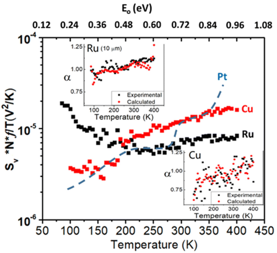 | ||
| Fig. 12 Temperature dependence of the normalized noise of a Pt NW (blue dashed curve) fabricated by substrate step lithography and Ru (black squares) and Cu (red squares) metal-line resistors fabricated at imec. Also shown are comparisons of values of the frequency dependence, α, that were measured (black squares) or predicted by the Dutta–Horn model of 1/f noise (red circles) for Ru (upper inset) and Cu (lower inset), showing good agreement. Adapted from ref. 71 with permission. Copyright 2019 American Institute of Physics. | ||
When NWs are cooled to low temperature, enhanced fluctuations can be observed. Fig. 13(a) shows resistance vs. temperature measurements from ∼5 K to ∼70 mK for a Bi NW fabricated via substrate step lithography.53 An increase in resistance is observed with decreasing temperature due to localization and electron–electron interactions. As the temperature decreases, the spread in measurements increases. Fig. 13(b) shows that this resistance spread is due to random jumps in resistance that are similar to RTN in semiconductor devices (e.g., Fig. 5).53,54,56,62,90,106 Charge trapping does not occur in metallic NWs owing to the high density of free carriers in the conduction band, so fluctuations in scattering rates due to carrier-defect interactions are the most likely origin of the RTN. Similar resistance fluctuations are shown in Fig. 14(a) for a Bi film at 70 mK and in Fig. 14(b) for a Pt film at 250 mK.54
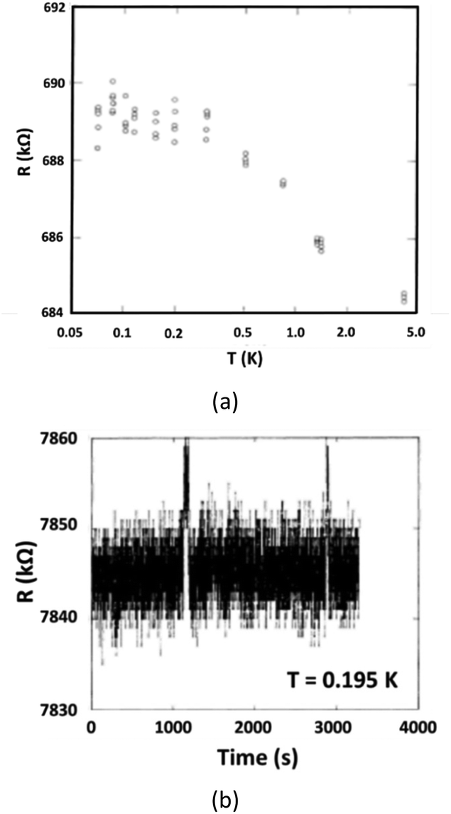 | ||
| Fig. 13 (a) Resistance vs. temperature for a Bi wire with L = 60 μm and diameter d = 46 nm fabricated via substrate step lithography. (b) Resistance at T = 0.195 K as a function of time for a Bi film with L = 16 μm, width W = 8 μm, and thickness t = 7 nm, fabricated in the same batch as the wires of (a). The rapid fluctuations with an envelope of about ±10 Ω are due to system noise. Large switching events at times of ∼1200 s and ∼2900 s are characteristic of RTN. Adapted from ref. 53 with permission. Copyright 1987 The American Physical Society. | ||
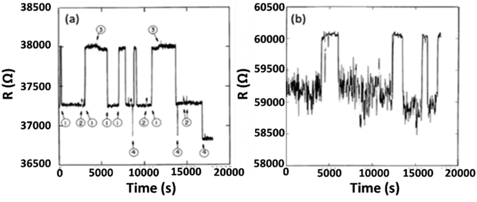 | ||
| Fig. 14 (a) Resistance vs. time at T = 70 mK for an ∼8 nm thick Bi film with L = 10 μm and W = 4 μm. Numbers denote different fluctuators. (b) Resistance vs. time at 250 mK for a 1 nm thick Pt film with L = 7 μm and W = 5 μm. Adapted from ref. 54 with permission. Copyright 1987 Institute of Physics. | ||
In 1987 Beutler, Meisenheimer, and Giordano compared the fluctuations in Fig. 13 and 14 with those predicted by the theory of universal conductance fluctuations (UCF) by Feng, Lee, and Stone.15,53,54,85 UCF theory predicts that the motion of one strong scattering center leads to conductance fluctuations of order q2/h, where h is Planck's constant.15,85 They find that fluctuations in Fig. 13 and 14 are ∼10× larger than predicted by UCF.
Also in 1987, following the approach of Martin, Pelz and Clarke showed that the fluctuating interference of electrons in the local environment of a moving defect or impurity (“local-interference”) can lead to conductance fluctuations that are smaller than UCF predictions, and more consistent with the 1/f noise observed in metals.86,180,181 In 1989 Birge et al. then measured low-temperature conductance fluctuations in thin Bi films that are much smaller than those in Fig. 13 and 14.182 Fluctuation magnitudes in these films agree well with predictions of the local-interference model of Pelz and Clarke.86,182 Taken together, it is likely that the “giant” conductivity fluctuations in Fig. 13 and 14 are most likely due to the stochastic motions and/or reconfiguration of larger defect and/or impurity complexes in the bulk of the Bi NWs and films.15,53,54,85,86,108
When a magnetic field is applied to a metal wire that exhibits UCF, the theory of Feng, Lee, and Stone predicts a 2× decrease in 1/f noise magnitude from the zero-field value.15,18,183 This 2× reduction is due to a corresponding decrease in noise-producing transmission channels caused by magnetization-induced dephasing.15,85,183–186 Spin-orbit coupling is a key consideration in both electron localization and UCF.3,15,85,183–186 Clear evidence of time-dependent UCF (TDUCF) is shown in Fig. 15(a) for Li, Fig. 15(b) for Ag, and Fig. 15(c) for AuPd NWs, which vary from low to high spin–orbit coupling.184–186 In all three cases in Fig. 15, TDUCF is observed at temperatures low enough to suppress scattering due to local interference and/or magnetic impurities (if present). At higher temperatures, a mixture of noise due to TDUCF, local interference, and/or magnetic impurities is found, leading to increases in relative noise magnitudes. These results confirm the significance of TDUCF in nanowires with lower (Li) or higher (Ag and AuPd) spin–orbit coupling.184–186
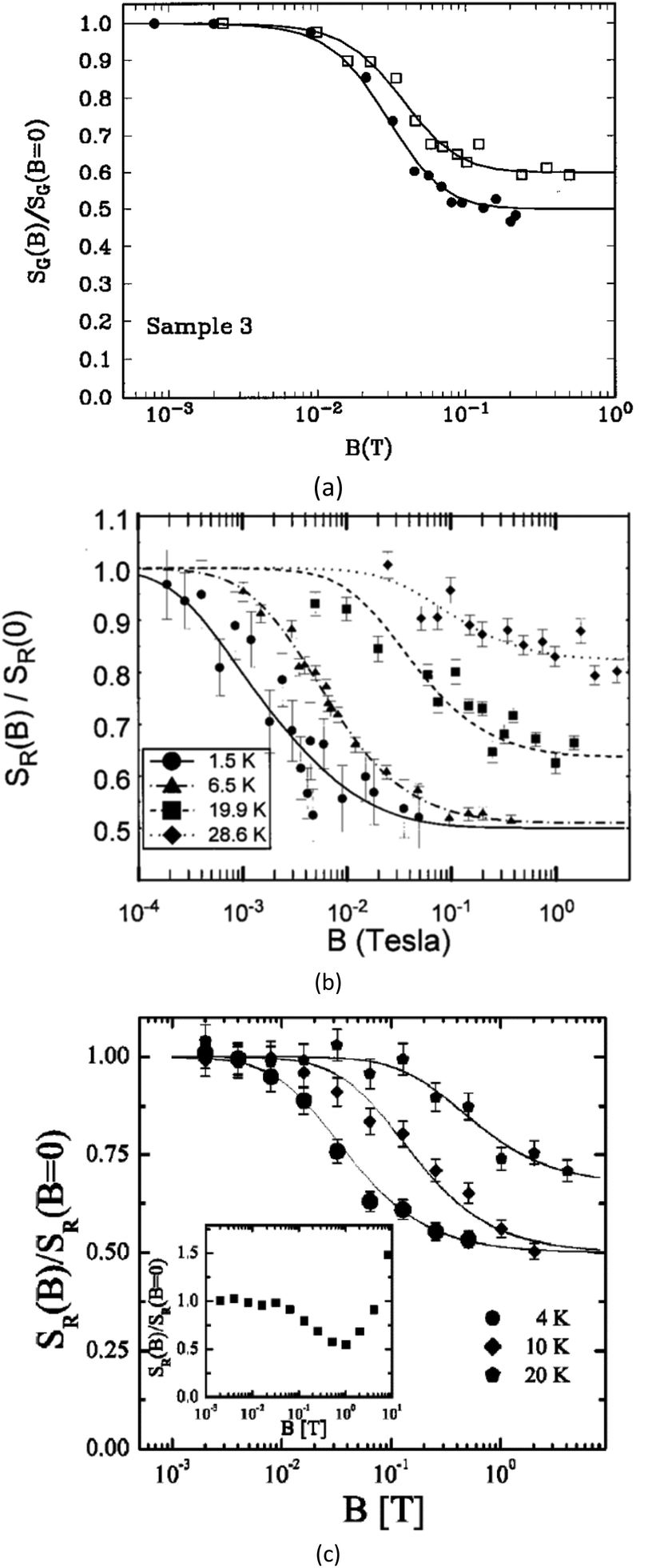 | ||
| Fig. 15 Ratios of 1/f noise magnitudes with, SR(B), and without, SR(0), magnetic fields applied to (a) Li (reproduced from ref. 184 with permission; copyright 1997 The American Physical Society), (b) Ag (reproduced from ref. 185 with permission; copyright 1999 The American Physical Society), and (c) AuPd NWs (reproduced from ref. 186 with permission; copyright 2004 The American Physical Society). The 2× reduction in SR(B)/SR(0) at low temperatures is due to universal conductance fluctuations. At higher temperatures, fluctuations due to local interference increase values of SR(B)/SR(0). The upturn in SR(B)/SR(0) in the inset of (c) is due to process-introduced magnetic impurities. | ||
While defects and impurities are critical to the LF noise and RTN of metallic NWs, it is usually not possible to identify their microstructures.55,66,86,95 As an exception, mobile hydrogen has been identified as a scattering impurity in Pd films by Zimmerman and Webb.98 Also, Fig. 16 and 17 show conductivity fluctuations and LF noise in lithographically defined RuO2 and IrO2 NWs, respectively. In each case, the LF noise and RTN are attributed to TDUCF caused by mobile defects and/or impurities in the NWs, with oxygen vacancies a likely source in each case.65,75 The normalized noise magnitudes for the IrO2 NWs in Fig. 17 are 1–2 orders of magnitude higher than those of the Pt, Ru, and Cu NWs in Fig. 1, 3, 9, and 12. This suggests a higher defect density, mobility, and/or scattering cross-section for the IrO2 NWs in Fig. 17 than for Pt, Ru, and Cu NWs.
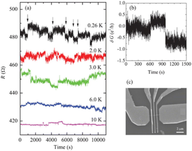 | ||
| Fig. 16 (a) Resistance at five temperatures for a RuO2 NW with length L = 1.5 μm and diameter d = 67 nm. Data at 6.0 K, 3.0 K, 2.0 K, and 0.26 K are offset by 10 Ω, 20 Ω, 30 Ω, and 40 Ω, respectively, for clarity. (b) Conductance variation δG = G − 〈G〉 vs. time at 0.26 K. (c) Scanning electron microscope (SEM) image of lithographically defined NW. Reproduced from ref. 65 with permission. Copyright 2011 American Institute of Physics. | ||
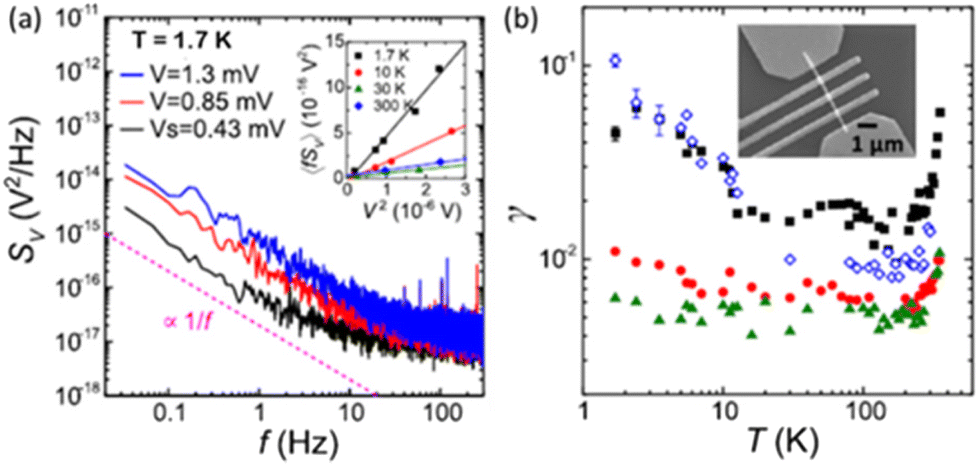 | ||
| Fig. 17 (a) SVvs. f and T for an IrO2 NW with L = 0.9 μm and d = 147 nm; 〈fSV〉 vs. V2 is shown in the inset. (b) γ = SVNcf/V2vs. T for IrO2 NWs from 1.7 K to 350 K. The inset is a SEM image of a NW. Dimensions are L = 1.9 μm, d = 143 nm (solid black squares); L = 1.0 μm, d = 123 nm (solid red circles); L = 0.75 μm, d = 125 nm (solid green triangles); and L = 0.9 μm, d = 147 nm (open blue diamonds). Reproduced from ref. 75 with permission. Copyright 2023 American Institute of Physics. | ||
As illustrated in Fig. 18, significant RTN can also be found in metallic nanobridges, which are essentially short, tapered NWs.57,58,87,89 The conductivity fluctuations are dominated by the restriction at the base of the lithographically defined nanobridge in Fig. 18(a). Ralls et al. verified the crystallinity of these Cu nanobridges,57 but still find significant RTN at room temperature, as shown in Fig. 18(b). These results demonstrate that, even in the absence of grain boundaries, large conductivity fluctuations can be found in metallic NWs and other nanoscale structures.57,58,87,89 Ralls and Buhrman discuss the resulting fluctuations in terms of a “defect glass,” in which the two-level fluctuations observed in Fig. 18(b) result from slow, stochastic transitions of the system from one configurational state to another.58 These results show that, while defects and impurities can enhance 1/f noise and RTN in metallic NWs, significant noise due to fluctuations in scattering rates can occur even in clean, highly ordered nano-systems at room temperature.57,58 The universality of these scattering processes helps explain why LF noise is observed in so many different types of materials and devices.55,57,58,66,95
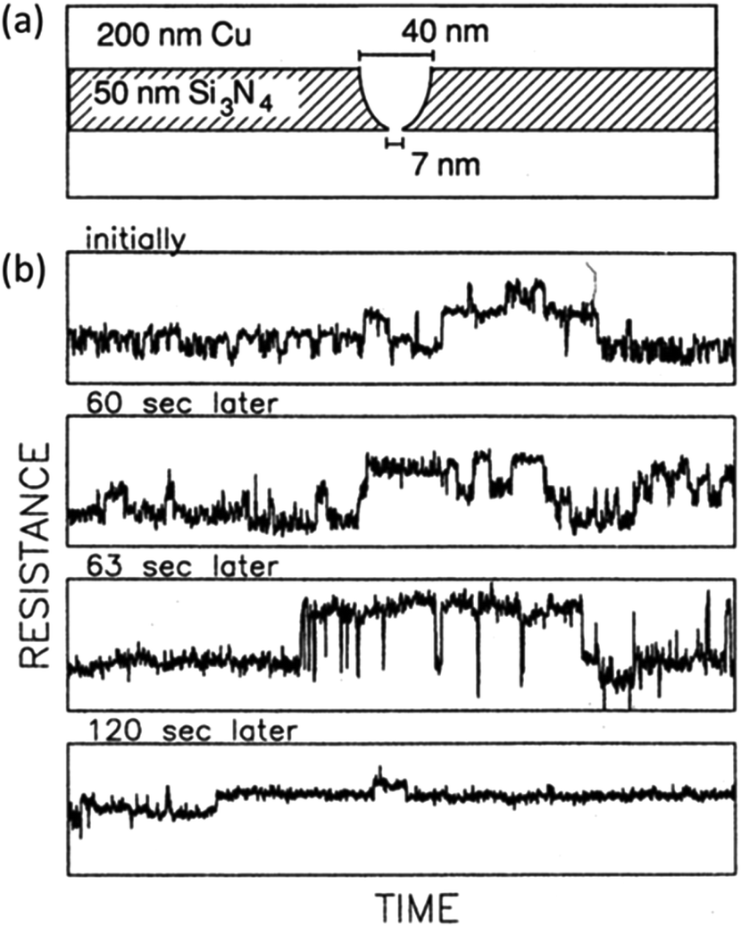 | ||
| Fig. 18 (a) Schematic diagram of Cu nanobridge and (b) resistance vs. time snapshots (0.2 s each) at 300 K, illustrating the time evolution of defect-induced scattering in these structures at room temperature. Reproduced from ref. 57 with permission. Copyright 1989 The American Physical Society. | ||
IV. Semiconducting nanowires
Ralls, et al., showed in 1984 that MOS transistors at the ∼1 μm scale exhibit RTN at cryogenic temperatures due to the alternating capture and emission of electrons at a single, prominent oxide trap. Heating the device and decreasing the gate voltage closer to Vth increased the number of active defects, leading to 1/f noise.84 Kirton and Uren provide a thorough review of the intense activity that followed this initial report in the late 1980s.56 It is therefore no surprise that, with continuing Moore's Law scaling of MOS structures, semiconducting NWs with much smaller dimensions exhibit LF noise and RTN in proportions that vary with device geometry, channel and insulator materials, defect concentrations, bias, temperature, etc.59–74Fig. 19 shows LF noise measurements for a GaAs NW with AlGaAs insulating layer and PtPd Schottky wrap gate.64 For many of the NWs, LF noise spectra are similar to the red curve for the L = 60 nm device in Fig. 19(a). An inverse-area dependence is observed for the noise magnitude, consistent with number-fluctuation noise viaeqn (15).64 This result shows that contact noise is not significant in these devices.60,64,187,188 In some cases, e.g., the blue and green curves for larger devices in Fig. 19(a), generation–recombination (G–R) noise is observed. The G–R noise correlates with gate leakage, suggesting that individual defects in AlGaAs are contributing Lorentzian noise at frequencies above 100–300 Hz.64 A likely candidate for the responsible defect is the DX center, a well-known electron trap in AlGaAs, which is most often an isolated Si donor.64,189–191
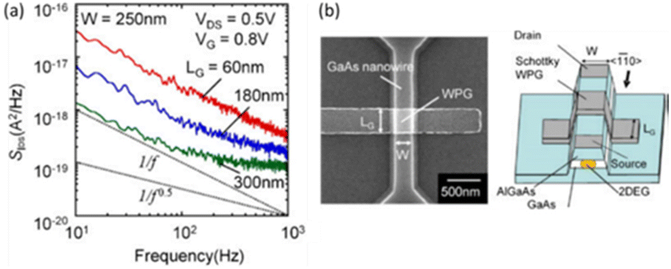 | ||
| Fig. 19 (a) Current noise power-spectral densities of Schottky wrap-gate (WPG) GaAs/AlGaAs NW transistors with W = 250 nm and varying L. (b) Top view and schematic cross-section. Adapted from ref. 64 with permission. Copyright 2011 Institute of Physics. | ||
RTN and LF noise are observed in InGaAs NW MOSFETs with gate dielectrics of 0.5 nm Al2O3/4.0 nm LaAlO3 in Fig. 20(a) and (b) and with a 3.5 nm Al2O3 gate oxide in Fig. 20(c).67 The RTN in Fig. 20(a) and the higher-noise device in Fig. 20(c) are attributed to number fluctuations due to discrete charge trapping in the gate oxide; the 1/f noise in the lower-noise device in Fig. 20(c) is attributed to mobility fluctuations.67 The device is operating in the subthreshold regime of device operation in Fig. 20(a), in which small perturbations in surface potential due to charge capture and emission can lead to significant changes in current. About a 7% change in current is observed for each discrete trapping or emission event in Fig. 20(a). The mobility-fluctuation noise of the devices of Fig. 20 is analyzed by the authors within the framework of the Hooge mobility fluctuation model.67 However, as noted in Section II, the Hooge model does not correctly characterize or parameterize the noise of semiconductor devices.55,66,76,95,128,132,192 It is therefore more likely that the noise of these NWs is due to a mixture of number fluctuations (eqn (8)–(16))73,108,112 and mobility fluctuations due to carrier scattering by defects and/or impurity atoms within NW channels, e.g., as described by the local interference model of Pelz and Clarke.86,180,181
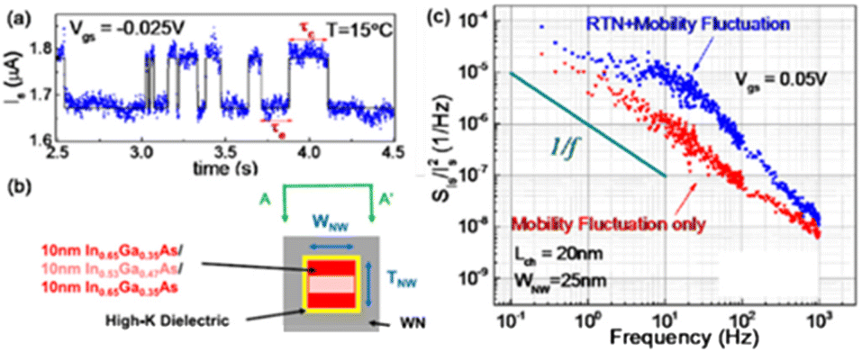 | ||
| Fig. 20 (a) RTN at VDS = 50 mV for InGaAs NW MOSFET with geometry illustrated schematically in (b). The gate dielectric of the device in (a) is 0.5 nm Al2O3/4 nm LaAlO3. (c) Normalized noise power spectral density vs. frequency for two InGaAs NW MOSFETs with 3.5 nm Al2O3 dielectrics: one showing RTN and the other showing LF noise. Adapted from ref. 67 with permission. Copyright 2015 Institute of Electrical and Electronics Engineers. | ||
The Hooge mobility model is similarly used to interpret the LF noise observed in the Si NW MOSFETs of Fig. 21, primarily because the gate-voltage dependence of the noise follows eqn (2) instead of eqn (15) in the subthreshold region of device operation in Fig. 20(a).63 As noted above, deviations from an inverse (VGS – VTH)2 dependence can occur for a several reasons in MOS devices, e.g., strongly varying spatial or energy distributions of defects, as often found.66,73,90,107,117–124,128,154,192 Noise vs. temperature measurements usually are required to determine if this is the case.55,66,73,90,95 In the absence of such variation in defect spatial or energy distribution, carrier scattering by defects and/or impurity atoms within the NW channels is the most likely origin for the “excess” LF noise above that expected from number fluctuations in the subthreshold region of device operation in Fig. 21(a).55,66,86,95,180,181
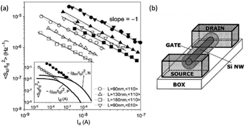 | ||
| Fig. 21 (a) Average normalized drain–current spectral density at |VDS| = 50 mV and f = 10 Hz vs. drain current IDS for n-type (solid symbols) and p-type (open symbols) Si NW transistors with SiO2 gate dielectric thickness of 4 nm and effective radius of ∼40 nm, as shown schematically in (b). The noise data of 90 nm n- and p-type SNWTs in the 〈110〉 direction are compared with lines of (constant × (gM/IDS)2) in the inset. Adapted from ref. 63 with permission. Copyright 2009 Institute of Electrical and Electronics Engineers. | ||
Fig. 22 shows RTN for a vertical InAs/InGaAsSb/GaSb NW tunnel FET with a 20 nm InAs channel diameter69 and Al2O3/HfO2 gate dielectric, and Fig. 23 shows RTN for a silicon NW on a silicon-on-insulator (SOI) wafer with a SiO2 gate dielectric.59 The “giant” RTN observed in each case is far too large to be caused by simple charge exchange between the NW channel and traps in the gate dielectric.59,69,76 Moreover, the scattering effectiveness of charged border traps decreases strongly with distance between the channel and the trap.59,69,76,138 Thus, fluctuations in scattering rates caused by random dopant atoms in the NW channel and/or changes in charge state or configuration of bulk defect clusters in the NW channel are much more likely causes of the giant RTN observed in the NWs of Fig. 22 and 23.59,69,76,139–144 The fluctuating activation and passivation of interface traps may also play a role in the LF noise of devices in Si MOS devices in which there are simultaneously high densities of dangling Si bonds and high concentrations of hydrogen at the SiO2 interface.76,132,193 This is an area of active current investigation.76
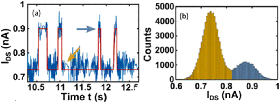 | ||
| Fig. 22 (a) RTN at a temperature of 150 K in a vertical InAs/InGaAsSb/GaSb NW tunnel FET with a 20 nm InAs channel diameter and Al2O3/HfO2 gate dielectric with effective oxide thickness of 1.4 nm. (b) Histograms of current values measured in the higher conductivity (gold) and lower conductivity (blue) states of the device, corresponding to the respective arrows in (a). Adapted from ref. 69 with permission. Copyright 2017 American Chemical Society. | ||
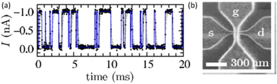 | ||
| Fig. 23 (a) RTN for a silicon NW on a silicon-on-insulator (SOI) wafer with length of 200 nm and width of 30 nm with SiO2 gate oxide thickness of 24 nm. VGS = 0.5 V, VDS = −6 mV. (b) Top view of NW. Adapted from ref. 59 with permission. Copyright 2006 Springer. | ||
Nanosheets are essentially flattened and stacked versions of NWs being considered for next-generation Si MOS technologies.72,81 The noise of gate-all-around devices with Si nanosheet channels and high-K gate dielectrics is shown in Fig. 24. LF noise due to number fluctuations is observed,72 most likely because each measured device consists of 22 fins in parallel with two stacked nanosheets per fin. Hence, multiple defects and/or impurities are contributing to the noise. The normalized noise of the devices of Fig. 24 is comparable to or less than that of other advanced MOS technologies, indicating relatively low concentrations of border traps in the gate dielectrics and/or bulk defects in the nanosheets.72,194–196 In studies by Hellenbrand, et al., border traps also are found to be primarily responsible for the LF noise of III–V NWs, tunnel FETs, and planar MOSFETs.197,198
 | ||
| Fig. 24 (a) Schematic diagrams of gate-all-around GAA nFETs with two vertically stacked Si nanosheets. (b) Drain current noise power spectral density (left y-axis) and normalized power spectral density (right y-axis) as a function of frequency for a 15 nm nanosheet width device at different gate voltages. Adapted from ref. 72 with permission. Copyright 2020 Institute of Electrical and Electronics Engineers. | ||
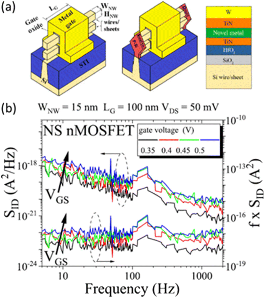
Fig. 25 summarizes results from detailed evaluations of RTN before total-ionizing-dose irradiation of gate-all-around (GAA) Si MOS NW transistors with high-K dielectrics. Each device contains four fins and two NWs.74 As the gate voltage and/or device temperature is varied, LF noise with or without RTN is observed, depending on the gate voltage. Fig. 25 shows significant RTN at room temperature, especially for VGT ≡ VGS − VTH at 0.2 V and 0.3 V. Primarily 1/f noise is observed for VGT = 0.1 V and VGT = 0.6 V. Using a hidden Markov model and measured ratios of capture and emission times, it is inferred that only a few prominent defects lead to the observed RTN in Fig. 25.74,199–201 Under the conventional assumption that these RTN are due to charge exchange with border traps in a standard number fluctuation model, estimates of trap locations were inferred, with defects identified in both the near-interfacial SiO2 and the HfO2 layer of the dielectric stack.74 However, in at least some cases, this typical interpretation74,199–201 may not be complete or correct,76,77 as we now discuss.
 | ||
| Fig. 25 Gate-to-threshold voltage dependence of IDS at 295 K for a GAA NW nFET with L ≈ 25 nm, 8 nm diameter, and 1.8 nm HfO2/1 nm gate dielectric; a transmission-electron-microscope image of the structure is shown in (b). VDS = 50 mV; VGT ≡ VGS − VTH. Note that each value of VGT has a different y-axis scale. Adapted from ref. 74 with permission. Copyright 2021 Institute of Electrical and Electronics Engineers. | ||
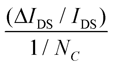
Table 1 summarizes predicted and observed RTN magnitudes for the data of Fig. 25; predictions use the simple number fluctuation model of eqn (12) without mobility fluctuations.76,110,111 At VGT = 0.2–0.3 V, where RTN are most active, Table 1 shows that ratios of observed magnitudes of current fluctuations are up to ∼2.5× larger than expectations based on the number fluctuation model of eqn (12). This demonstrates the importance of mobility fluctuations in the RTN of these devices.76,77,110,111 At these voltages, the strength of scattering needed to account for the RTN magnitudes is much greater than likely from remote Coulomb scattering from border traps.59,69,76,77,138
| n c (1012 cm−2) | V GT (V) | 1/NC (10−3) NMF prediction | ΔIDS/IDS (10−3) measured |
|
|---|---|---|---|---|
| 2.2 ± 0.1 | 0.10 | 9.0 ± 0.5 | 8.0 ± 1.0 | 0.90 ± 0.15 |
| 4.3 ± 0.2 | 0.20 | 4.5 ± 0.25 | 8.5 ± 1.0 | 1.9 ± 0.3 |
| 6.5 ± 0.4 | 0.30 | 3.0 ± 0.2 | 7.5 ± 1.0 | 2.5 ± 0.3 |
| 8.6 ± 0.4 | 0.40 | 2.3 ± 0.1 | 2.8 ± 0.3 | 1.2 ± 0.2 |
| 11 ± 0.5 | 0.50 | 1.8 ± 0.1 | 2.8 ± 0.3 | 1.6 ± 0.3 |
| 13 ± 0.5 | 0.60 | 1.5 ± 0.1 | 1.9 ± 0.3 | 1.25 ± 0.25 |
These results suggest that the RTN of the Si NW MOSFETs of Fig. 25 are caused by a mixture of border traps in the high-K dielectric, bulk defects in the NW channels, and interface traps.74,76,77 The responsible bulk defects may be random dopant atoms and/or defect clusters.74,76,77,139–144 For interface traps to contribute to LF noise and/or RTN, the rate-limiting step is more likely to be hydrogen-mediated defect activation and passivation, which can occur on ms to s time scales, than charge capture and emission, which typically occur on μs time scales for interface traps.76
Fig. 26 and 27 show the evolution of the LF noise vs. frequency and temperature for as-processed and irradiated devices. Consistent with the results in Fig. 25, spectral slopes range from ∼1/f (no RTN) to ∼1/f2 (significant RTN).74 Inferred defect-energy distributions from the Dutta–Horn model of LF noise66,95 are shown in Fig. 26(b) and 27(b). Some active defects in as-processed devices are passivated during irradiation, some defects are newly activated via irradiation, and other defects are remarkably stable through the full irradiation and measurement sequence.74,77
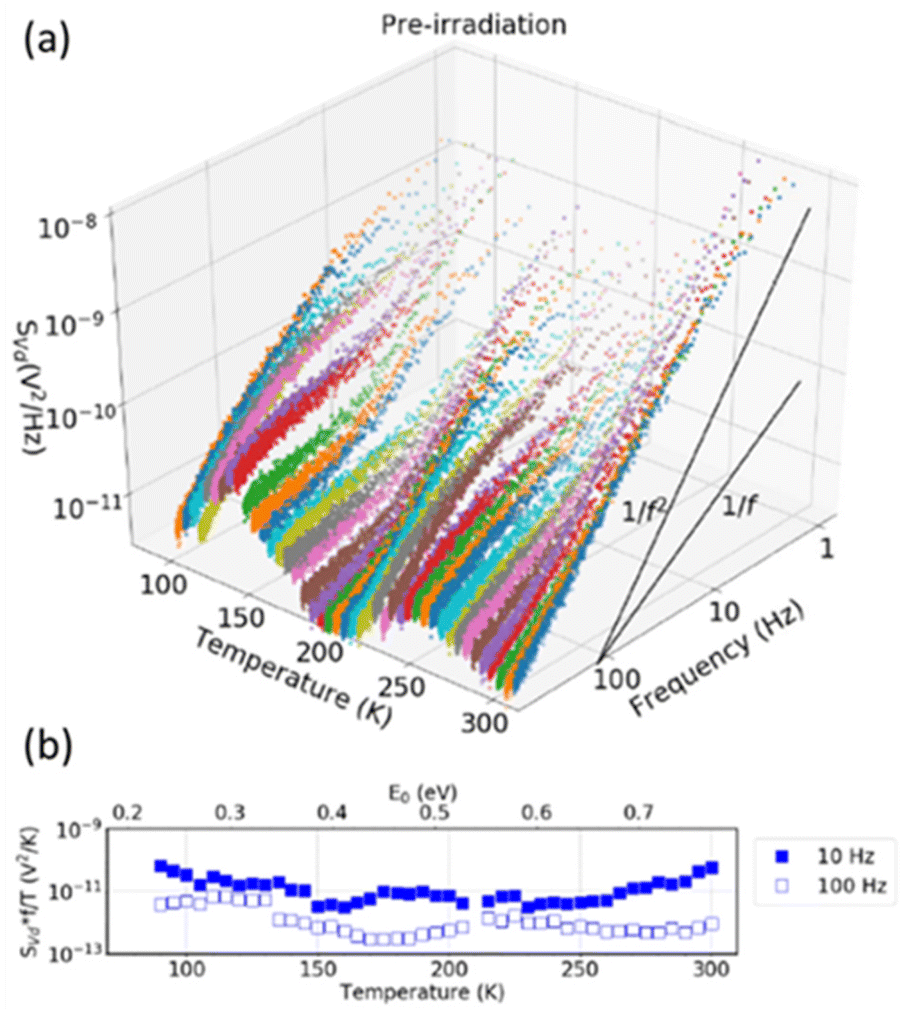 | ||
| Fig. 26 (a) Frequency and temperature dependences of SVd at f = 1–400 Hz and T = 90–300 K and (b) temperature dependence of the normalized noise at f = 10 and 100 Hz for the as-processed GAA NW nFETs of Fig. 25. Noise measurements were performed at VGT = 0.4 V and Vd = 50 mV. When significant RTN is observed, the normalized noise at 10 Hz significantly exceeds that at 100 Hz. Adapted from ref. 74 with permission. Copyright 2021 Institute of Electrical and Electronics Engineers. | ||
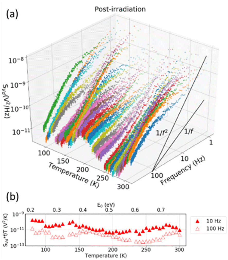 | ||
| Fig. 27 (a) Frequency and temperature dependences of SVd at f = 1–400 Hz and T = 90–300 K and (b) temperature dependence of normalized SVd at f = 10 and 100 Hz for GAA NW nFETs of Fig. 25 and 26 irradiated to 2 Mrad(SiO2) and annealed for 1 h at VGS = 0.5 V. Noise measurements were performed at VGT = 0.4 V and Vd = 50 mV. When significant RTN is observed, the normalized noise at 10 Hz significantly exceeds that at 100 Hz. Adapted from ref. 74 with permission. Copyright 2021 Institute of Electrical and Electronics Engineers. | ||
That border traps primarily lead to 1/f noise and bulk defects evidently lead to large RTN in the Si MOS NWs of Fig. 25–27 is the reverse of the trend inferred for early-generation InGaAs NWs in Fig. 20. There RTN was attributed to border traps and LF noise was attributed to fluctuations in carrier scattering rates due to bulk defects.67 This trend reversal may result from improvements in NW fabrication over the last ∼10 years.
Finally, Fig. 28 shows that, when the NWs of Fig. 25–27 are operated under conditions for which large RTN is not observed, the slope of the gate-voltage dependence, 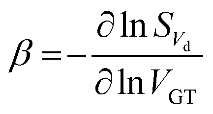 , is generally close to 2, as expected from eqn (15) for noise caused primarily by border traps with approximately uniform energy and spatial distributions.55,66,95 Hence, neither quantum confinement, series resistance, nor trap-trap interaction effects appear to be significantly affecting the LF noise of these NWs.202,203 Instead, the results of Fig. 26 and 27 are consistent with previous studies on planar MOSFETs and FinFETs with SiO2 and/or high-K gate dielectrics (e.g., Fig. 7 and 8) for which O vacancies and complexes with hydrogen most likely lead to the observed 1/f noise.66,73,74,90,107,109,112–114,120–123,131–134,145–147,204–210
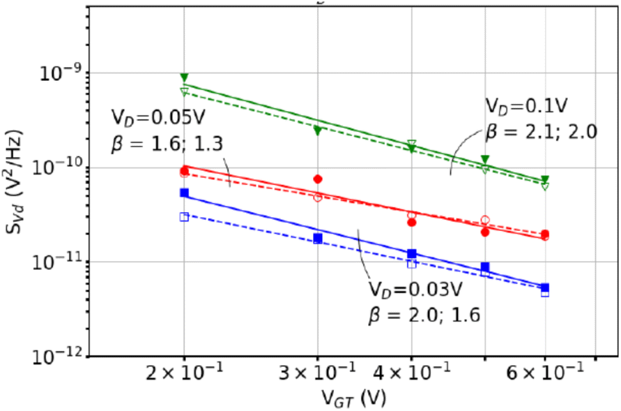 | ||
| Fig. 28 Gate-voltage dependence of SVd at VDS = 30 mV, 50 mV, and 100 mV for as-processed (closed symbols, solid lines) and irradiated (open symbols, dashed lines) GAA NW nFETs. The device was irradiated to 1 Mrad(SiO2) with 10 keV X-rays at VGS = 0.5 V. Reproduced from ref. 74 with permission. Copyright 2021 Institute of Electrical and Electronics Engineers. | ||
The wide range of noise magnitudes and frequency dependences observed in Fig. 25–28 strongly suggest that the noise of analog ICs built using semiconducting NWs may be quite challenging to model with confidence as a function of operating voltage and temperature.211–217 Until these issues are resolved, users will have difficulty in assessing and assuring the accuracy and precision of systems relying on NWs or similarly scaled MOS devices.81 These manufacturability and reliability issues must be addressed before high-volume application of NW-based ICs is possible in critical commercial, defense, space, and scientific applications.214–217
V. Conclusions
Defects and impurities play critical roles in the LF noise of metallic and semiconducting NWs. Effective defect-energy distributions can be obtained from noise versus temperature measurements in conjunction with the Dutta–Horn model of 1/f noise. For metallic NWs, fluctuations in scattering rates caused by defect and/or impurity motion and/or reconfiguration of a bulk defect complex are often the dominant sources of LF noise and RTN. With few exceptions, the nature of these defects and impurities are unknown.The capture and emission of carriers by border traps in adjacent or surrounding dielectrics often dominate LF noise and RTN for NWs in MOSFET configurations. Comparative studies of device performance, reliability, and radiation response, often supported by first principles calculations, enable identification of border traps leading to LF noise in semiconductor NWs and other MOS devices passivated with SiO2 and/or high-K dielectric layers. In particular, oxygen vacancies and/or their complexes with hydrogen can lead to LF noise and/or RTN. Defect-passivation treatments such as high-pressure annealing in hydrogen or deuterium have been effective in reducing LF noise and RTN in semiconductor devices. Bulk defects and/or impurities also can contribute significantly to the LF noise, RTN, and device-to-device variations of semiconducting NWs. Reducing defect densities and variability in response are therefore crucial steps to enable high-volume manufacturing of ICs relying on NWs for critical terrestrial and space applications.
Conflicts of interest
There are no conflicts to declare.Acknowledgements
I thank D. E. Beutler, S. Beyne, S. Bonaldo, G. X. Duan, N. Giordano, M. Gorchichko, T. Grasser, M. J. Johnson, K. Li, D. Linten, J. T. Masden, T. L. Meisenheimer, D. Natelson, S. T. Pantelides, R. A. Reed, R. D. Schrimpf, J. H. Scofield, E. Simoen, H. D. Xiong, C. X. Zhang, and E. X. Zhang for stimulating discussions.References
- P. W. Anderson, Phys. Rev., 1961, 124, 41–53 CrossRef CAS.
- D. C. Licciardello and D. J. Thouless, J. Phys. C: Solid State Phys., 1975, 8, 4157–4170 CrossRef.
- D. J. Thouless, Phys. Rev. Lett., 1977, 39, 1167–1169 CrossRef CAS.
- E. Abrahams, P. W. Anderson, D. C. Licciardello and T. V. Ramakrishan, Phys. Rev. Lett., 1979, 42, 673–676 CrossRef.
- N. Giordano, W. Gilson and D. E. Prober, Phys. Rev. Lett., 1979, 43, 725–728 CrossRef CAS.
- P. W. Anderson, D. J. Thouless, E. Abrahams and D. S. Fisher, Phys. Rev. B: Condens. Matter Mater. Phys., 1980, 22, 3519–3526 CrossRef.
- N. Giordano, Phys. Rev. B: Condens. Matter Mater. Phys., 1980, 22, 5634–5654 CrossRef.
- J. T. Masden and N. Giordano, Phys. Rev. Lett., 1982, 49, 819–822 CrossRef CAS.
- A. E. White, M. Tinkham, W. J. Skocpol and D. C. Flanders, Phys. Rev. Lett., 1982, 48, 1752–1755 CrossRef CAS.
- W. J. Skocpol, L. D. Jackel, E. L. Hu, R. E. Howard and L. A. Fetter, Phys. Rev. Lett., 1982, 49, 951–955 CrossRef CAS.
- P. A. Lee and T. V. Ramakrishnan, Rev. Mod. Phys., 1985, 57, 287–337 CrossRef CAS.
- W. D. Williams and N. Giordano, Phys. Rev. B: Condens. Matter Mater. Phys., 1986, 33, 8146–8154 CrossRef CAS PubMed.
- K. K. Choi, D. C. Tsui and S. C. Palmateer, Phys. Rev. B: Condens. Matter Mater. Phys., 1986, 33, 8216–8227 CrossRef CAS PubMed.
- J. J. Lin and N. Giordano, Phys. Rev. B: Condens. Matter Mater. Phys., 1987, 35, 545–556 CrossRef CAS PubMed.
- P. A. Lee, A. D. Stone and H. Fukuyama, Phys. Rev. B: Condens. Matter Mater. Phys., 1987, 35, 1039–1070 CrossRef PubMed.
- D. E. Beutler and N. Giordano, Phys. Rev. B: Condens. Matter Mater. Phys., 1988, 38, 8–19 CrossRef CAS PubMed.
- B. Kramer and A. McKinnon, Rep. Prog. Phys., 1993, 56, 1459–1564 CrossRef.
- G. Bergmann, Phys. Rep., 1984, 107, 1–58 CrossRef CAS.
- A. V. Herzog, P. Xiong, F. Sharif and R. C. Dynes, Phys. Rev. Lett., 1996, 76, 668–671 CrossRef CAS PubMed.
- D. Natelson, R. L. Willett, K. W. West and L. N. Pfeiffer, Phys. Rev. Lett., 2001, 86, 1821–1824 CrossRef CAS PubMed.
- J. J. Lin and J. P. Bird, J. Phys.: Condens. Matter, 2002, 14, R501 CrossRef CAS.
- I. van Weperen, B. Tarasinski, D. Eeltink, V. S. Pribiag, S. R. Plissard, E. P. A. M. Bakkers, L. P. Kouwenhoven and M. Wimmer, Phys. Rev. B: Condens. Matter Mater. Phys., 2015, 91, 201413(R) CrossRef.
- S. Sett, K. Das and A. K. Raychaudhuri, J. Phys.: Condens. Matter, 2017, 29, 115301 CrossRef PubMed.
- Y. Aharonov and D. Bohm, Phys. Rev., 1959, 115, 485–491 CrossRef.
- J. Kondo, Rep. Prog. Phys., 1964, 32, 37–49 CAS.
- N. Andrei, K. Furuka and J. H. Lowenstein, Rev. Mod. Phys., 1983, 55, 331–402 CrossRef.
- C. P. Umbach, S. Washburn, R. B. Laibowitz and R. A. Webb, Phys. Rev. B: Condens. Matter Mater. Phys., 1984, 30, 4048–4051 CrossRef CAS.
- R. A. Webb, S. Washburn, C. P. Umbach and R. B. Laibowitz, Phys. Rev. Lett., 1985, 54, 2697–2699 Search PubMed.
- G. L. Chen and N. Giordano, Phys. Rev. Lett., 1991, 66, 209–211 CrossRef CAS PubMed.
- V. Chandrasekhar, P. Santhanam, N. A. Penebre, R. A. Webb, H. Vloeberghs, C. Van Haesendonck and Y. Bruynseraede, Phys. Rev. Lett., 1994, 72, 2053–2056 CrossRef CAS PubMed.
- M. A. Blachly and N. Giordano, Phys. Rev. B: Condens. Matter Mater. Phys., 1995, 51, 12537–12550 CrossRef CAS PubMed.
- K. Hong and N. Giordano, Phys. Rev. B: Condens. Matter Mater. Phys., 1995, 51, 9855–9862 CrossRef CAS PubMed.
- F. Schopfer, C. Bauerle, W. Rabaud and L. Saminadayar, Phys. Rev. Lett., 2003, 90, 056801 CrossRef PubMed.
- F. Pierre, A. B. Gougam, A. Anthore, H. Pothier, D. Esteve and N. O. Birge, Phys. Rev. B: Condens. Matter Mater. Phys., 2003, 68, 085413 CrossRef.
- P. Mohanty and R. A. Webb, Phys. Rev. Lett., 2003, 91, 066604 CrossRef CAS PubMed.
- F. Mallet, J. Ericsson, D. Mailly, S. Unlubayir, D. Reuter, A. Melnikov, A. D. Wieck, T. Micklitz, A. Rosch, T. A. Costi, L. Saminadayar and C. Bauerle, Phys. Rev. Lett., 2006, 97, 226804 CrossRef CAS PubMed.
- G. M. Alzoubi and N. O. Birge, Phys. Rev. Lett., 2006, 97, 226803 CrossRef PubMed.
- H. O. H. Churchill, V. Fatemi, K. Grove-Rasmussen, M. T. Deng, P. Caroff, H. Q. Xu and C. M. Marcus, Phys. Rev. B: Condens. Matter Mater. Phys., 2003, 87, 241401(R) CrossRef.
- M. T. Deng, S. Vaitiekenas, E. B. Hansen, J. Danon, M. Leijnse, K. Flensberg, J. Nygård, P. Krogstrup and C. M. Marcus, Science, 2016, 354, 1557–1562 CrossRef CAS PubMed.
- J. S. Langer and V. Ambegaokar, Phys. Rev., 1967, 164, 498–510 CrossRef.
- N. Giordano, Phys. Rev. Lett., 1988, 61, 2137–2140 CrossRef CAS PubMed.
- N. Giordano, Phys. Rev., 1991, 43, 160–174 CAS.
- A. Bezryadin, C. N. Lau and M. Tinkham, Nature, 2000, 404, 971–974 CrossRef CAS PubMed.
- M. Tian, J. Wang, J. S. Kurtz, Y. Liu, M. H. W. Chan, T. S. Mayer and T. S. Mallouk, Phys. Rev. B: Condens. Matter Mater. Phys., 2005, 71, 104521 CrossRef.
- Y. J. Doh, A. J. van Dam, A. L. Roest, E. P. A. M. Bakkers, L. P. Kouwenhouven and S. De Fransceschi, Science, 2005, 309, 272–275 CrossRef CAS PubMed.
- J. E. Mooij and Y. V. Najarov, Nat. Phys., 2006, 2, 169–172 Search PubMed.
- L. P. Rokhinson, X. Y. Liu and J. K. Furdyna, Nat. Phys., 2012, 8, 795–799 Search PubMed.
- M. T. Deng, C. L. Yu, G. Y. Huang, M. Larsson, P. Caroff and H. Q. Xu, Nano Lett., 2012, 12, 6414–6419 CrossRef CAS PubMed.
- Ö. Gül, H. Zhang, J. D. S. Bommer, M. W. A. de Moor, D. Car, S. R. Plissard, E. P. A. M. Bakkers, A. Geresdi, K. Watanabe, T. Taniguchi and L. P. Kouwenhoven, Nat. Nanotechnol., 2018, 13, 192–197 CrossRef PubMed.
- C. Jia, Z. Lin, Y. Huang and X. Duan, Chem. Rev., 2019, 119, 9074–9135 CrossRef CAS PubMed.
- D. M. Fleetwood and N. Giordano, Phys. Rev. Lett., 1983, 50, 450–453 CrossRef CAS.
- D. M. Fleetwood and N. Giordano, Phys. Rev. B: Condens. Matter Mater. Phys., 1985, 31, 1157–1160 CrossRef CAS PubMed.
- D. E. Beutler, T. L. Meisenheimer and N. Giordano, Phys. Rev. Lett., 1987, 58, 1240–1243 CrossRef CAS PubMed.
- T. L. Meisenheimer, D. E. Beutler and N. Giordano, Jpn. J. Appl. Phys., 1987, 26, 695–696 CrossRef CAS.
- M. B. Weissman, Rev. Mod. Phys., 1988, 60, 537–571 CrossRef CAS.
- M. J. Kirton and M. J. Uren, Adv. Phys., 1989, 38, 367–468 CrossRef CAS.
- K. S. Ralls, D. C. Ralph and R. A. Buhrman, Phys. Rev. B: Condens. Matter Mater. Phys., 1989, 40, 11561–11570 CrossRef CAS PubMed.
- K. S. Ralls and R. A. Buhrman, Phys. Rev. B: Condens. Matter Mater. Phys., 1991, 44, 5800–5817 CrossRef PubMed.
- M. Hofheinz, X. Jehl, M. Sanquer, G. Molas, M. Vinet and S. Deleonibus, Eur. Phys. J. B, 2006, 54, 299–307 CrossRef CAS.
- S. Reza, G. Bosman, M. S. Islam, T. I. Kamins, S. Sharma and R. S. Williams, IEEE Trans. Nanotechnol., 2006, 5, 523–529 Search PubMed.
- A. Bid, A. Bora and A. K. Raychaudhuri, Nanotechnology, 2006, 17, 152–156 CrossRef.
- H. D. Xiong, W. Wang, Q. Li, C. A. Richter, J. S. Suehle, W. K. Hong, T. Lee and D. M. Fleetwood, Appl. Phys. Lett., 2007, 91, 053107 CrossRef.
- C. Wei, Y.-Z. Xiong, X. Zhou, N. Singh, S. C. Rustagi, G. Q. Lo and D.-L. Kwong, IEEE Electron Device Lett., 2009, 30, 668–671 CAS.
- K. Miura, Y. Shiratori and S. Kasai, Jpn. J. Appl. Phys., 2011, 50, 06GF18 CrossRef.
- A.-S. Lien, L. Y. Wang, C. S. Chu and J.-J. Lin, Phys. Rev. B: Condens. Matter Mater. Phys., 2011, 84, 155432 CrossRef.
- D. M. Fleetwood, IEEE Trans. Nucl. Sci., 2015, 62, 1462–1486 CAS.
- M. Si, N. J. Conrad, S. Shin, J. Gu, J. Zhang, M. A. Alam and P. D. Ye, IEEE Trans. Electron Devices, 2015, 62, 3508–3515 Search PubMed.
- S. Ren, M. Si, K. Ni, X. Wan, J. Chen, S. Chang, X. Sun, E. X. Zhang, R. A. Reed, D. M. Fleetwood, P. Ye, S. Cui and T.-P. Ma, IEEE Trans. Nucl. Sci., 2015, 62, 2888–2893 CAS.
- E. Memisevic, M. Hellenbrand, E. Lind, A. R. Persson, S. Sant, A. Schenk, J. Svensson, R. Wallenberg and L.-E. Wernersson, Nano Lett., 2017, 17, 4373–4380 CrossRef CAS PubMed.
- G. Liu, S. Rumyantsev, M. A. Bloodgood, T. T. Salguero, M. Shur and A. A. Balandin, Nano Lett., 2017, 17, 377–383 CrossRef CAS PubMed.
- D. M. Fleetwood, S. Beyne, R. Jiang, S. E. Zhao, P. Wang, S. Bonaldo, M. W. McCurdy, Zs. Tőkei, I. De Wolf, K. Croes, E. X. Zhang, M. L. Alles, R. D. Schrimpf, R. A. Reed and D. Linten, Appl. Phys. Lett., 2019, 114, 203501 CrossRef.
- A. V. de Oliveira, A. Veloso, C. Claeys, N. Horiguchi and E. Simoen, IEEE Electron Device Lett., 2020, 41, 317–320 CAS.
- D. M. Fleetwood, IEEE Trans. Nucl. Sci., 2020, 67, 1216–1240 CAS.
- M. Gorchichko, E. X. Zhang, P. Wang, S. Bonaldo, R. D. Schrimpf, R. A. Reed, D. Linten, J. Mitard and D. M. Fleetwood, IEEE Trans. Nucl. Sci., 2021, 68, 687–696 CAS.
- P.-Y. Chen, C.-Y. Wu, R.-T. Wang, S.-P. Chiu, S. Kirchner, S.-S. Yeh and J.-J. Lin, Appl. Phys. Lett., 2023, 122, 143102 CrossRef.
- D. M. Fleetwood, Appl. Phys. Lett., 2023, 122, 173504 CrossRef CAS.
- S. Bonaldo and D. M. Fleetwood, Appl. Phys. Lett., 2023, 122, 173508 CrossRef CAS.
- R. H. Dennard, F. H. Gaensslen, H.-N. Yu, V. L. Rideout, E. Bassous and A. R. LeBlanc, IEEE J. Solid-State Circuits, 1974, 9, 256–268 Search PubMed.
- G. E. Moore, Advances in Resist Technology and Processing XII, 1995, vol. 2438, pp. 2–17 Search PubMed.
- S. E. Thompson and S. Parthasarathy, Mater. Today, 2006, 9, 20–25 CrossRef CAS.
- D. M. Fleetwood, IEEE Trans. Nucl. Sci., 2021, 68, 509–545 CAS.
- D. Natelson, R. L. Willett, K. W. West and L. N. Pfeiffer, Appl. Phys. Lett., 2000, 77, 1991–1993 CrossRef CAS.
- N. M. Zimmerman, J. H. Scofield, J. V. Mantese and W. W. Webb, Phys. Rev. B: Condens. Matter Mater. Phys., 1986, 34, 773–777 CrossRef CAS PubMed.
- K. S. Ralls, W. J. Skocpol, L. D. Jackel, R. E. Howard, L. A. Fetter, R. W. Epworth and D. M. Tennant, Phys. Rev. Lett., 1984, 52, 228–231 CrossRef CAS.
- S. Feng, P. A. Lee and A. D. Stone, Phys. Rev. Lett., 1986, 56, 1960–1963 CrossRef CAS PubMed.
- J. Pelz and J. Clarke, Phys. Rev. B: Condens. Matter Mater. Phys., 1987, 36, 4479–4482 CrossRef PubMed.
- C. T. Rogers and R. A. Buhrman, Phys. Rev. Lett., 1985, 55, 859–862 CrossRef CAS PubMed.
- M. J. Kirton and M. J. Uren, Appl. Phys. Lett., 1986, 48, 1270–1272 CrossRef CAS.
- K. R. Farmer, C. T. Rogers and R. A. Buhrman, Phys. Rev. Lett., 1987, 58, 2255–2258 CrossRef CAS PubMed.
- T. Grasser, Microelectron. Reliab., 2012, 52, 39–70 CrossRef CAS.
- J. B. Johnson, Phys. Rev., 1928, 32, 97–109 CrossRef CAS.
- H. Nyquist, Phys. Rev., 1928, 32, 110–113 CrossRef CAS.
- F. N. Hooge, Phys. Lett., 1969, 29A, 139–140 CrossRef.
- F. N. Hooge, T. G. M. Kleinpenning and L. K. J. Vandamme, Rep. Prog. Phys., 1981, 44, 479–532 CrossRef.
- P. Dutta and P. M. Horn, Rev. Mod. Phys., 1981, 53, 497–516 CrossRef CAS.
- D. M. Fleetwood, D. E. Beutler, J. T. Masden and N. Giordano, J. Appl. Phys., 1987, 61, 5308–5313 CrossRef CAS.
- D. M. Fleetwood and N. Giordano, Phys. Rev. B: Condens. Matter Mater. Phys., 1983, 27, 667–671 CrossRef CAS.
- N. M. Zimmerman and W. W. Webb, Phys. Rev. Lett., 1988, 61, 889–892 CrossRef CAS PubMed.
- J. W. Eberhard and P. M. Horn, Phys. Rev. B: Condens. Matter Mater. Phys., 1978, 18, 6681–6693 CrossRef CAS.
- D. M. Fleetwood and N. Giordano, Phys. Rev. B: Condens. Matter Mater. Phys., 1983, 28, 3625–3628 CrossRef CAS.
- R. D. Black, P. J. Restle and M. B. Weissman, Phys. Rev. Lett., 1983, 51, 1476–1479 CrossRef CAS.
- J. H. Scofield, J. V. Mantese and W. W. Webb, Phys. Rev. B: Condens. Matter Mater. Phys., 1985, 32, 736–742 CrossRef CAS PubMed.
- J. Pelz and J. Clarke, Phys. Rev. Lett., 1985, 55, 738–741 CrossRef CAS PubMed.
- J. Bernamont, Ann. Phys., 1937, 7, 71–140 Search PubMed.
- A. van der Ziel, Physica, 1950, XVI, 359–372 CrossRef.
- S. Machlup, J. Appl. Phys., 1954, 25, 341–343 CrossRef.
- D. M. Fleetwood, H. D. Xiong, Z. Y. Lu, C. J. Nicklaw, J. A. Felix, R. D. Schrimpf and S. T. Pantelides, IEEE Trans. Nucl. Sci., 2002, 49, 2674–2683 CAS.
- S. Christenson, I. Lundstrom and C. Svennson, Solid-State Electron., 1968, 11, 797–812 CrossRef.
- D. M. Fleetwood and J. H. Scofield, Phys. Rev. Lett., 1990, 64, 579–582 CrossRef CAS PubMed.
- K. K. Hung, P. K. Ko, C. Hu and Y. C. Cheng, IEEE Trans. Electron Devices, 1990, 37, 654–665 CrossRef.
- G. Ghibaudo, O. Roux, C. Nguyen-Duc, F. Balestra and J. Brini, Phys. Status Solidi (a), 1991, 124, 571–581 CrossRef.
- J. H. Scofield and D. M. Fleetwood, IEEE Trans. Nucl. Sci., 1991, 38, 1567–1577 CAS.
- D. M. Fleetwood, P. S. Winokur, R. A. Reber Jr., T. L. Meisenheimer, J. R. Schwank, M. R. Shaneyfelt and L. C. Riewe, J. Appl. Phys., 1993, 73, 5058–5074 CrossRef CAS.
- D. M. Fleetwood, T. L. Meisenheimer and J. H. Scofield, IEEE Trans. Electron Devices, 1994, 41, 1953–1964 CrossRef CAS.
- G. Ghibaudo and T. Boutchacha, Microelectron. Reliab., 2002, 42, 573–582 CrossRef.
- D. M. Fleetwood, IEEE Trans. Nucl. Sci., 1992, 39, 269–271 Search PubMed.
- D. M. Fleetwood, M. R. Shaneyfelt and J. R. Schwank, Appl. Phys. Lett., 1994, 64, 1965–1967 CrossRef CAS.
- D. M. Fleetwood, M. R. Shaneyfelt, W. L. Warren, J. R. Schwank, T. L. Meisenheimer and P. S. Winokur, Microelectron. Reliab., 1995, 35, 403–428 CrossRef.
- D. M. Fleetwood, IEEE Trans. Nucl. Sci., 1996, 43, 779–786 CAS.
- T. Grasser, B. Kaczer, W. Goes, H. Reisinger, T. Aichinger, P. Hehenberger, P. J. Wagner, F. Schanovsky, J. Franco, M. T. Luque and M. Nehliebel, IEEE Trans. Electron Devices, 2011, 58, 3652–3666 CAS.
- D. M. Fleetwood, Microelectron. Reliab., 2018, 80, 266–277 CrossRef CAS.
- W. Goes, Y. Wimmer, A.-M. El-Sayeda, G. Rzepaa, M. Jecha, A. L. Shluger and T. Grasser, Microelectron. Reliab., 2018, 87, 286–320 CrossRef CAS.
- C. Schleich, D. Waldhoer, K. Waschneck, M. W. Feil, H. Reisinger, T. Grasser and M. Waltl, IEEE Trans. Electron Devices, 2022, 68, 4016–4021 Search PubMed.
- X. Luo, E. X. Zhang, P. F. Wang, K. Li, D. Linten, J. Mitard, R. A. Reed, D. M. Fleetwood and R. D. Schrimpf, IEEE Trans. Device Mater. Reliab., 2023, 23, 153–161 CAS.
- M. H. Tsai and T. P. Ma, IEEE Trans. Nucl. Sci., 1992, 39, 2178–2185 CAS.
- D. M. Fleetwood, E. X. Zhang, R. D. Schrimpf and S. T. Pantelides, IEEE Trans. Nucl. Sci., 2022, 69, 1105–1119 CAS.
- C. X. Zhang, E. X. Zhang, D. M. Fleetwood, R. D. Schrimpf, S. Dhar, S.-H. Ryu, X. Shen and S. T. Pantelides, IEEE Electron Device Lett., 2013, 34, 117–119 CAS.
- J. H. Scofield, N. Borland and D. M. Fleetwood, IEEE Trans. Electron Devices, 1994, 41, 1946–1952 CrossRef CAS.
- Y. Nemirovsky, I. Brouk and C. G. Jakobson, IEEE Trans. Electron Devices, 2001, 48, 921–927 CrossRef.
- J. H. Scofield, N. Borland and D. M. Fleetwood, Appl. Phys. Lett., 2000, 76, 3248–3250 CrossRef CAS.
- D. M. Fleetwood, W. L. Warren, M. R. Shaneyfelt, R. A. B. Devine and J. H. Scofield, J. Non-Cryst. Solids, 1995, 187, 199–205 CrossRef CAS.
- D. M. Fleetwood, M. J. Johnson, T. L. Meisenheimer, P. S. Winokur, W. L. Warren and S. C. Witczak, IEEE Trans. Nucl. Sci., 1997, 44, 1810–1817 CAS.
- G. X. Duan, J. A. Hachtel, E. X. Zhang, C. X. Zhang, D. M. Fleetwood, R. D. Schrimpf, R. A. Reed, J. Mitard, D. Linten, L. Witters, N. Collaert, A. Mocuta, A. V-Y. Thean, M. F. Chisholm and S. T. Pantelides, IEEE Trans. Device Mater. Reliab., 2016, 16, 541–548 CAS.
- C. D. Liang, P. Wang, S. E. Zhao, E. X. Zhang, M. L. Alles, D. M. Fleetwood, R. D. Schrimpf, R. Ma, Y. Su and S. Koester, IEEE Trans. Nucl. Sci., 2018, 65, 1227–1238 CAS.
- E. G. Ioannidis, C. A. Dimitriadis, S. Haendler, R. A. Bianchi, J. Jomaah and G. Ghibaudo, Solid-State Electron., 2012, 76, 54–59 CrossRef CAS.
- M. von Haartman, B. G. Malm and M. Ostling, IEEE Trans. Electron Devices, 2006, 53, 836–843 CAS.
- F. N. Hooge and L. K. J. Vandamme, Phys. Lett. A, 1978, 66, 315–316 CrossRef.
- F. B. McLean and H. E. Boesch Jr., IEEE Trans. Nucl. Sci., 1989, 36, 1772–1783 CAS.
- A. Asenov, A. R. Brown, J. H. Davies, S. Kaya and G. Slavcheva, IEEE Trans. Electron Devices, 2003, 50, 1837–1852 CrossRef CAS.
- N. Tega, H. Miki, M. Yamaoka, H. Kume, T. Mine, T. Ishida, Y. Mori, R. Yamada and K. Torii, Proc. 2008 IEEE Intl. Reliab. Phys. Sympos, Phoenix, AZ, 2008, pp. 541–546 Search PubMed.
- J. P. Campbell, L. C. Yu, K. P. Cheung, J. Qin, J. S. Suehle, A. Oates and K. Sheng, Proc., 2009 IEEE Intl. Conf. IC Design Technol, Austin, TX, 2009, pp. 17–20 Search PubMed.
- V. Goiffon, G. R. Hopkinson, P. Magnan, F. Bernard, G. Rolland and O. Saint-Pe, IEEE Trans. Nucl. Sci., 2009, 56, 2132–2141 Search PubMed.
- V. Goiffon, P. Magnan, P. Martin-Gonthier, C. Virmontois and M. Gaillardin, IEEE Electron Device Lett., 2011, 32, 773–775 CAS.
- J. R. Srour and J. W. Palko, IEEE Trans. Nucl. Sci., 2013, 60, 1740–1766 CAS.
- H. D. Xiong, D. M. Fleetwood, B. K. Choi and A. L. Sternberg, IEEE Trans. Nucl. Sci., 2002, 49, 2718–2723 Search PubMed.
- T. Roy, E. X. Zhang, Y. S. Puzyrev, X. Shen, D. M. Fleetwood, R. D. Schrimpf, G. Koblmueller, R. Chu, C. Poblenz, N. Fichtenbaum, C. S. Suh, U. K. Mishra, J. S. Speck and S. T. Pantelides, Appl. Phys. Lett., 2011, 99, 203501 CrossRef.
- J. Chen, Y. S. Puzyrev, C. X. Zhang, E. X. Zhang, M. W. McCurdy, D. M. Fleetwood, R. D. Schrimpf, S. T. Pantelides, S. W. Kaun, E. C. Kyle and J. S. Speck, IEEE Trans. Nucl. Sci., 2013, 60, 4080–4086 CAS.
- J. Chen, Y. S. Puzyrev, R. Jiang, E. X. Zhang, M. W. McCurdy, D. M. Fleetwood, R. D. Schrimpf, S. T. Pantelides, A. Arehart, S. A. Ringel, P. Saunier and C. Lee, IEEE Trans. Nucl. Sci., 2015, 62, 2423–2430 CAS.
- R. Jiang, X. Shen, J. Fang, P. Wang, E. X. Zhang, J. Chen, D. M. Fleetwood, R. D. Schrimpf, S. W. Kaun, E. C. H. Kyle, J. S. Speck and S. T. Pantelides, IEEE Trans. Device Mater. Reliab., 2018, 18, 364–376 CAS.
- S. Bonaldo, S. E. Zhao, A. O'Hara, M. Gorchichko, E. X. Zhang, S. Gerardin, A. Paccagnella, N. Waldron, N. Collaert, V. Putcha, D. Linten, S. T. Pantelides, R. A. Reed, R. D. Schrimpf and D. M. Fleetwood, IEEE Trans. Nucl. Sci., 2020, 67, 210–220 CAS.
- J. Robertson, K. Xiong and S. J. Clark, Thin Solid Films, 2006, 496, 1–7 CrossRef CAS.
- A.-M. El-Sayed, M. B. Watkins, V. V. Afanas'ev and A. L. Shluger, Phys. Rev. B: Condens. Matter Mater. Phys., 2014, 89, 125201 CrossRef.
- M. Waltl, B. Stampfer, G. Rzepa, B. Kaczer and T. Grasser, Microelectron. Reliab., 2020, 114, 113746 CrossRef CAS.
- K. Li, X. Luo, M. W. Rony, M. Gorchichko, G. Hiblot, S. Van Huylenbroeck, A. Jourdain, M. L. Alles, R. A. Reed, E. X. Zhang, D. M. Fleetwood and R. D. Schrimpf, IEEE Trans. Nucl. Sci., 2023, 70, 442–448 Search PubMed.
- T. L. Meisenheimer and D. M. Fleetwood, IEEE Trans. Nucl. Sci., 1990, 37, 1696–1702 CAS.
- T. L. Meisenheimer, D. M. Fleetwood, M. R. Shaneyfelt and L. C. Riewe, IEEE Trans. Nucl. Sci., 1991, 38, 1297–1303 Search PubMed.
- T. Grasser, W. Goes, Y. Wimmer, F. Schanovsky, G. Rzepa, M. Waltl, K. Rott, H. Reisinger, V. V. Afanas'ev, A. Stesmans, A.-M. El-Sayed and A. L. Shluger, Tech. Dig. - Int. Electron Devices Meet., 2014, 21.1.1–21.1.4 Search PubMed.
- P. Wang, C. Perini, A. O. Hara, B. R. Tuttle, E. X. Zhang, H. Gong, L. Dong, C. Liang, R. Jiang, W. Liao, D. M. Fleetwood, R. D. Schrimpf, E. M. Vogel and S. T. Pantelides, IEEE Trans. Nucl. Sci., 2018, 65, 156–163 CAS.
- A. A. Balandin, Nat. Nanotechnol., 2013, 8, 549–555 CrossRef CAS PubMed.
- V. K. Sangwan, H. N. Arnold, D. Jariwala, T. J. Marks, L. J. Lauhon and M. C. Hersam, Nano Lett., 2013, 13, 4351–4355 CrossRef CAS PubMed.
- J. Renteria, R. Samnakay, S. L. Rumyantsev, C. Jiang, P. Goli, M. S. Shur and A. A. Balandin, Appl. Phys. Lett., 2014, 104, 153104 CrossRef.
- X. Xie, D. Sarkar, W. Liu, J. Kang, O. Marinov, M. J. Deen and K. Banerjee, ACS Nano, 2014, 8, 5633–5640 CrossRef CAS PubMed.
- B. Stampfer, F. Zhang, Y. Yu. Illarionov, T. Knobloch, P. Wu, M. Waltl, A. Grill, J. Appenzeller and T. Grasser, ACS Nano, 2018, 12, 5368–5375 CrossRef CAS PubMed.
- P. Wang, H. Kalita, A. Krishnaprasad, D. Dev, A. O'Hara, R. Jiang, E. X. Zhang, D. M. Fleetwood, R. D. Schrimpf, S. T. Pantelides and T. Roy, IEEE Trans. Nucl. Sci., 2019, 66, 1584–1591 CAS.
- Y. Yu. Illarionov, T. Knobloch, M. Jech, M. Lanza, D. Akinwande, M. I. Vexler, T. Mueller, M. C. Lemme, G. Fiori, F. Schwierz and T. Grasser, Nat. Commun., 2020, 11, 3385 CrossRef CAS PubMed.
- P. G. Collins, M. S. Fuhrer and A. Zettl, Appl. Phys. Lett., 2000, 76, 894–896 CrossRef CAS.
- M. Ishigami, J. H. Chen, E. D. Williams, D. Tobias, Y. F. Chen and M. S. Fuhrer, Appl. Phys. Lett., 2006, 88, 203116 CrossRef.
- Y.-M. Lin, J. Appenzeller, J. Knoch, Z. Chen and P. Avouris, Nano Lett., 2006, 6, 930–936 CrossRef CAS PubMed.
- D. Tobias, M. Ishigami, A. Tselev, P. Barbara, E. D. Williams, C. J. Lobb and M. S. Fuhrer, Phys. Rev. B: Condens. Matter Mater. Phys., 2008, 77, 033407 CrossRef.
- Y.-M. Lin and P. Avouris, Nano Lett., 2008, 8, 2119–2125 CrossRef CAS PubMed.
- A. N. Pal, S. Ghatak, V. Kochat, E. S. Sneha, A. Sampathkumar, S. Raghavan and A. Ghosh, ACS Nano, 2011, 5, 2075–2081 CrossRef CAS PubMed.
- A. Rehman, A. Krajewska, B. Stonio, K. Pavlov, G. Cywinski, D. Lioubtchenko, W. Knap, S. Rumyantsev and J. M. Smulko, Appl. Phys. Lett., 2021, 118, 242102 CrossRef CAS.
- P. K. Darmawi-Iskandar, A. M. Aaron, E. X. Zhang, B. L. Bhuva, J. S. Kauppila, J. L. Davidson, M. L. Alles, D. M. Fleetwood and L. W. Massengill, IEEE Trans. Nucl. Sci., 2023, 449–455 Search PubMed.
- P. S. Winokur, E. B. Errett, D. M. Fleetwood, P. V. Dressendorfer and D. C. Turpin, IEEE Trans. Nucl. Sci., 1985, 32, 3954–3960 Search PubMed.
- J. R. Schwank and D. M. Fleetwood, Appl. Phys. Lett., 1988, 53, 770–772 CrossRef.
- K. Hess, B. Tuttle, F. Register and D. K. Ferry, Appl. Phys. Lett., 1999, 75, 3147 CrossRef CAS.
- Y. Mori, A. Shima, K. Takeda and R.-I. Yamada, Jpn. J. Appl. Phys., 2012, 51, 104101 CrossRef.
- H.-M. Kwon, I.-S. Han, S.-K. Kwon, J.-H. Jang, H.-Y. Kwak, W.-I. Choi, M.-L. Ha, J.-I. Lee, H.-S. Hwang and H.-D. Lee, IEEE Electron Device Lett., 2013, 34, 190–192 Search PubMed.
- G. Yang, D. Kim, J. W. Yang, S. Barraud, L. Brevard, G. Ghibaudo and J. W. Lee, Nanotechnology, 2020, 31, 415201 CrossRef CAS PubMed.
- J. W. Martin, Philos. Mag., 1971, 24, 555–566 CrossRef CAS.
- J. W. Martin, J. Phys. F: Met. Phys., 1972, 2, 842–853 CrossRef CAS.
- N. O. Birge, B. Golding and W. H. Haemmerle, Phys. Rev. Lett., 1989, 62, 195–198 CrossRef CAS PubMed.
- A. D. Stone, Phys. Rev. B: Condens. Matter Mater. Phys., 1989, 39, 10736–10743 CrossRef PubMed.
- J. S. Moon, N. O. Birge and B. Golding, Phys. Rev. B: Condens. Matter Mater. Phys., 1997, 15124–15132 CrossRef CAS.
- D. Hoadley, P. McConville and N. O. Birge, Phys. Rev. B: Condens. Matter Mater. Phys., 1999, 5617–5625 CrossRef CAS.
- A. Trionfi, S. Lee and D. Natelson, Phys. Rev. B: Condens. Matter Mater. Phys., 2004, 041304(R) CrossRef.
- C. J. Delker, Y. Zi, C. Yang and D. B. Janes, IEEE Trans. Electron Devices, 2013, 60, 2900–2905 CAS.
- N. Clement, X. L. Han and G. Larrieu, Appl. Phys. Lett., 2013, 103, 263504 CrossRef.
- J. R. Kirtley, T. N. Theis, P. M. Mooney and S. L. Wright, J. Appl. Phys., 1988, 83, 1541–1548 CrossRef.
- P. M. Mooney, J. Appl. Phys., 1990, 67, R1–R26 CrossRef CAS.
- D. J. Chadi and K. J. Chang, Phys. Rev. B: Condens. Matter Mater. Phys., 1989, 39, 10063–10074 CrossRef CAS PubMed.
- D. M. Fleetwood, Noise in Nanoscale Semiconductor Devices, ed. T. Grasser, Springer, New York, 2020, pp. 1–31 Search PubMed.
- J. Ding, E. X. Zhang, K. Li, X. Luo, M. Gorchichko and D. M. Fleetwood, IEEE Trans. Nucl. Sci., 2021, 68, 2724–2735 CAS.
- D. Jang, J. W. Lee, C.-W. Lee, J.-P. Colinge, L. Montès, J. I. Lee, G. T. Kim and G. Ghibaudo, Appl. Phys. Lett., 2011, 98, 133502 CrossRef.
- E. Simoen, M. G. C. de Andrade, M. Aoulaiche, N. Collaert and C. Claeys, IEEE Trans. Electron Devices, 2012, 59, 1272–1278 Search PubMed.
- E. Simoen, A. Veloso, P. Matagne, N. Collaert and C. Claeys, IEEE Trans. Electron Devices, 2018, 65, 1487–1492 CAS.
- M. Hellenbrand, E. Memiševic, M. Berg, O.-P. Kilpi, J. Svensson and L.-E. Wernersson, IEEE Electron Device Lett., 2017, 38, 1520–1523 CAS.
- M. Hellenbrand, O.-P. Kilpi, J. Svensson, E. Lind and L.-E. Wernersson, Microelectron. Eng., 2019, 215, 110986 CrossRef CAS.
- L. R. Rabiner, Proc. IEEE, 1989, 77, 257–286 CrossRef.
- G. Schwarz, Annu. Stat., 1978, 6, 461–464 Search PubMed.
- Z. Celik-Butler, P. Vasina and N. V. Amarasinghe, IEEE Trans. Electron Devices, 2000, 47, 646–648 CrossRef CAS.
- J. Zhuge, R. Wang, R. Huang, Y. Tian, L. Zhang, D.-W. Kim, D. Park and Y. Wang, IEEE Electron Device Lett., 2009, 30, 57–60 CAS.
- N. Clément, K. Nishiguchi, A. Fujiwara and D. Vuillaume, Nat. Commun., 2010, 1, 92 CrossRef PubMed.
- P. M. Lenahan and P. V. Dressendorfer, J. Appl. Phys., 1984, 55, 3495–3499 CrossRef CAS.
- D. M. Fleetwood, M. R. Shaneyfelt, L. C. Riewe, P. S. Winokur and R. A. Reber Jr., IEEE Trans. Nucl. Sci., 1993, 40(6), 1323–1334 CAS.
- X. J. Zhou, D. M. Fleetwood, I. Danciu, A. Dasgupta, S. A. Francis and A. D. Touboul, Appl. Phys. Lett., 2007, 91, 173501 CrossRef.
- T. Grasser, M. Waltl, K. Puschkarsky, B. Stampfer, G. Rzepa, G. Pobegen, H. Reisinger, H. Arimura and B. Kaczer, Proc. Intl. Reliab. Phys. Symp., 2017, 6A-2.1–6A-2.6 Search PubMed.
- F. Faccio, G. Borghello, E. Lerario, D. M. Fleetwood, R. D. Schrimpf, H. Gong, E. X. Zhang, P. Wang, S. Michelis, S. Gerardin, A. Paccagnella and S. Bonaldo, IEEE Trans. Nucl. Sci., 2018, 65, 164–174 CAS.
- D. M. Fleetwood, IEEE Trans. Nucl. Sci., 2018, 65, 1465–1481 CAS.
- M. Gorchichko, Y. R. Cao, E. X. Zhang, D. Yan, H. Gong, S. E. Zhao, P. Wang, R. Jiang, C. D. Liang, D. M. Fleetwood, R. D. Schrimpf, R. A. Reed and D. Linten, IEEE Trans. Nucl. Sci., 2020, 67, 245–252 CAS.
- C. Bogner, C. Schlunder, M. Waltl, H. Reisinger and T. Grasser, Proc. Intl. Reliab. Phys. Symp., 2023, 7A.2.1–7A.2.6 Search PubMed.
- M. Manghisoni, L. Ratti, V. Re, V. Speziali, G. Traversi and A. Candelori, IEEE Trans. Nucl. Sci., 2003, 50, 1827–1833 CAS.
- S. W. Nam, X. Jiang, Q. Xiong, D. Ham and C. M. Lieber, Proc. Natl. Acad. Sci. U. S. A., 2009, 106, 21035–21038 CrossRef CAS PubMed.
- P. Leroux, W. Van Koeckhoven, J. Verbeeck, M. Van Uffelen, S. Esqué, R. Ranz, C. Damiani and D. Hamilton, Fusion Eng. Des., 2014, 89, 2314–2319 CrossRef CAS.
- J. Singh, J. Ciavatti, K. Sundaram, J. S. Wong, A. Bandyopadhyay, X. Zhang, S. Li, A. Bellaouar, J. Watts, J. G. Lee and S. B. Samavedam, IEEE Trans. Electron Devices, 2018, 65, 31–37 CAS.
- V. Re, L. Gaioni, M. Manghisoni, L. Ratti, E. Riceputi and G. Traversi, IEEE Trans. Nucl. Sci., 2018, 65, 550–557 CAS.
- S. Andrić, F. Lindelöw, L. O. Fhager, E. Lind and L.-E. Wernersson, IEEE Trans. Microwave Theory Tech., 2022, 70, 1284–1291 Search PubMed.
| This journal is © The Royal Society of Chemistry 2023 |