
Synaptic plasticity and non-volatile memory characteristics in TiN-nanocrystal-embedded 3D vertical memristor-based synapses for neuromorphic systems†
Seyeong
Yang
a,
Taegyun
Kim
a,
Sunghun
Kim
a,
Daewon
Chung
a,
Tae-Hyeon
Kim
d,
Jung Kyu
Lee
a,
Sungjoon
Kim
b,
Muhammad
Ismail
a,
Chandreswar
Mahata
a,
Sungjun
Kim
 *a and
Seongjae
Cho
*c
*a and
Seongjae
Cho
*c
aDivision of Electronics and Electrical Engineering, Dongguk University, Seoul 04620, South Korea. E-mail: sungjun@dongguk.edu
bDepartment of Electrical and Computer Engineering, Seoul National University, Seoul 08826, South Korea
cDepartment of Electronic and Electrical Engineering, Ewha Womans University, Seoul 03760, South Korea. E-mail: felixcho@ewha.ac.kr
dSchool of Electrical and Computer Engineering, Georgia Institute of Technology, Atlanta, GA, 30332, USA
First published on 12th July 2023
Abstract
Although vertical configurations for high-density storage require challenging process steps, such as etching high aspect ratios and atomic layer deposition (ALD), they are more affordable with a relatively simple lithography process and have been employed in many studies. Herein, the potential of memristors with CMOS-compatible 3D vertical stacked structures of Pt/Ti/HfOx/TiN-NCs/HfOx/TiN is examined for use in neuromorphic systems. The electrical characteristics (including I–V properties, retention, and endurance) were investigated for both planar single cells and vertical resistive random-access memory (VRRAM) cells at each layer, demonstrating their outstanding non-volatile memory capabilities. In addition, various synaptic functions (including potentiation and depression) under different pulse schemes, excitatory postsynaptic current (EPSC), and spike-timing-dependent plasticity (STDP) were investigated. In pattern recognition simulations, an improved recognition rate was achieved by the linearly changing conductance, which was enhanced by the incremental pulse scheme. The achieved results demonstrated the feasibility of employing VRRAM with TiN nanocrystals in neuromorphic systems that resemble the human brain.
Introduction
With the development of the technology of the Internet of Things (IoT) and artificial intelligence (AI), the importance of high-storage memory has increased in accordance with the increasing demand for data transmission.1 NAND flash is currently in widespread use as non-volatile solid-state storage memory (particularly for high-capacity data storage) due to its relatively compact cell size and high integration capability.2–4 With the increased technological competition (such as the introduction of multilevel cells and vertical stacking) to satisfy the demand for expanded capacity, 3D vertical NAND flash has become commercially available, despite its slow write/erase speeds (μs–ms) and severely constrained endurance (∼105 cycles).5–8 In the pursuit of improved memory performance, new candidates for scaling are being examined, such as resistive random-access memory (RRAM), with its simple metal–insulator–metal (MIM) structures, high scalability, fast operating speed, low power consumption, and outstanding endurance.9–16 Utilizing the production platform already in place for DRAM or NAND flash is the most viable option for implementing RRAM as practical high-intensity memory.17 Moreover, 3D integration of RRAM with the current facilities offers ultrahigh-density data storage memory and completely leverages the maximum scalability.17In terms of architecture, 3D RRAM can be configured as either horizontal RRAM (HRRAM) or vertical RRAM (VRRAM).15,18–21 HRRAM is enlarged by stacking layers on top of a 2D crossbar array, which offers improved performance in terms of producing shorter RC delays and higher array sizes with less energy.18,19 By using planar deposition methods (such as physical vapor deposition (PVD)), HRRAM can be manufactured using a 2D crossbar array, allowing the combination of selector devices.18,19 In contrast, VRRAM employs atomic layer deposition (ALD) techniques for the switching layer and deep and high aspect ratio trenching to construct multilayer memory cells, which is challenging for incorporating selector devices.5,20,21 However, VRRAM is more cost-effective than HRRAM due to its relatively smaller lithography process. In comparison, HRRAM is defined in the lithography stage, increasing the number of lithography masks and process steps linearly as the number of stacked layers increases.22–24
The basic working mechanism of RRAM (or memristors) for storing or erasing data is the transformation between high and low resistance states in MIM cells by an external voltage.25 Diverse materials are employed as oxide layers between metal electrodes, with binary metal oxides (such as HfOx, NiOx, AlOx, and TiOx) being studied in particular.26–31 Of these, HfOx is CMOS compatible and offers many benefits, including a high dielectric constant (∼25) and a wide bandgap (∼6 eV).32,33 Moreover, HfOx-based RRAM relies on the formation and rupture of conductive filaments, which are produced by the migration of oxygen vacancies within the switching layer.34,35 Accordingly, it is important to determine the factors that improve reliability (especially in vertically stacked structures), because it is challenging within RRAM to handle the intrinsically and stochastically generated filaments. Among the various improvement techniques (such as doping, multilayer stacks, and interface engineering) to minimize fluctuation, inserting nanocrystals into the HfOx switching layer was selected in this study to enhance the resistive switching properties.36–44 In ITO/HfOx/ITO flexible RRAM devices, controlling the growth of conductive filaments in the amorphous-nanocrystalline HfOx switching layer achieves reproducible switching behavior.45 Here, Pt-NCs are introduced into the TiO2−x oxide layer to achieve reliable switching properties and low cycle-to-cycle variations.46 In addition, IrOx nanodot-embedded AlOx RRAM devices have attractive nonvolatile features, low variability, and excellent multilevel characteristics (MLC) for 3D applications.47 The presence of TiN nanoparticles deposited with ALD in Au/Ti/HfAlOx/TiN-NP/HfAlOx/ITO RRAM devices also facilitates improvements in the memory window to improve and implement conductance quantization and multilevel properties.48
In this paper, we present a Pt/Ti/HfOx/TiN-NCs/HfOx/TiN stack 3D vertical RRAM structure. Furthermore, a multilayer structure with the potential to be used in high-density 3D VRRAM is demonstrated using a HfOx switching layer with TiN-NCs fabricated using the ALD technique. Key memory properties (such as endurance and retention) are examined in comparison with a single device with a 2D planar structure to demonstrate stable switching at all layers of the VRRAM structure. Moreover, by measuring the potential and depression characteristics, excitatory post-synaptic current, and spike-timing-dependent plasticity, we successfully simulated synapses in a 3D configuration. We also demonstrate that a memristor is suitable as a synaptic device in neuromorphic systems by simulating pattern recognition using the MNIST database.
Experimental
2D single cell
A 2D planar single cell was fabricated using the following procedure. First, a hydrofluoric acid (HF) and sulfuric acid–peroxide mixture (SPM) cleaning procedure was followed before reactive sputtering was used to deposit a TiN layer of 100 nm thickness as the bottom electrode (BE) on a SiO2/Si substrate. Trimethylaluminum (TDMAHf) was used as a precursor and ozone (O3) was used as a reactant during the growth of a HfOx switching layer of 10 nm thickness using ALD (NCD, Lucida M300PL-O). The flow of events is as follows: TDMAHf feeding → N2 gas purge → O3 feeding → N2 gas purge. 97 cycles were conducted to grow the HfOx atom-by-atom at the stage temperature of 350 °C. Rapid thermal annealing (RTA) was applied as a heat treatment after a TiN nanocrystal layer of 2 nm thickness was generated by ALD with TDMATi and NH3. After the formation of TiN nanocrystals, a HfOx layer of 10 nm thickness was deposited to cover the TiN-NCs. After photolithography to create a 100 μm × 100 μm square pattern, a Ti layer of 10 nm thickness for adhesion and a Pt top electrode (TE) of 100 nm thickness were finally deposited using an e-beam evaporator.3D VRRAM
A Pt/HfOx/TiN-nanocrystal/HfOx/TiN VRRAM device was fabricated as follows (Fig. S1†): a plane electrode and a SiO2 dielectric layer were deposited alternately using RF reactive sputtering and plasma-enhanced chemical vapor deposition (PECVD), respectively. To create multilayer RRAM cells, trench holes were patterned and etched. A reactive ion etching system (Oxford RIE 80 plus) was used for dry etching SiO2 layers with CF4/Ar plasma and TiN layers with Cl2/Ar plasma. Then, the switching layers were deposited by thermal ALD (NCD, Lucida M300PL-O). A HfOx layer of 10 nm thickness was used with TEMAHf as a precursor and ozone (O3) was used as a reactant at 350 °C. A TiN nanocrystal layer of 2 nm thickness was then formed by rapid thermal annealing (RTA) at 400 °C for 30 s after deposition using ALD with TDMATi and NH3.Subsequently, a HfOx switching layer was deposited to cover the nanocrystal layer under the same conditions as mentioned previously. Then, a Ti adhesion layer of 10 nm thickness and a Pt electrode of 200 nm thickness were deposited using e-beam evaporation (ULVAC, FF-EB20). To apply ground to the plane electrode, the contact pads were patterned and etched. SiO2 was then etched on the top layer for the contact pads of M1 and M2. Subsequently, M2's contact pad was covered and only M1's contact pad was opened by etching TiN and SiO2, in that order. The electrical properties in DC and pulse modes were measured using a semiconductor parameter analyzer (Keithley 4200-SCS, Cleveland, OH, USA) and a 4225-PMU ultrafast module. The M1 cells employed a TiN layer directly on top of the passivation oxide, whereas the M2 cells used a TiN layer between the SiO2 layer as the bottom electrode. These two cells shared a common top electrode and a switching layer. The contact pad of each layer was grounded while the program and erase voltages were assigned to the pillar electrodes during the measurements.
Results and discussion
Fig. 1(a) and (b) display top and cross-sectional views of the 3D vertical RRAM structure. The memory cells were defined by a 10 μm diameter of holes formed by deeply etching multilayers stacked alternately with TiN plane electrodes and insulating SiO2 layers, which isolated the cells. In the TEM image (Fig. 1(c) and (d)), it is evident that TiN nanocrystals were introduced into the HfOx switching layer and that the ALD-deposited switching layer ensured outstanding step coverage. In previous studies, it was revealed that polycrystalline TiN (which is partially present in the TiN nanocrystal layer) enables uniform switching and improves switching properties (such as endurance and switching speed).48–50 To verify whether TiN nanocrystals were appropriately generated between the switching layers, energy dispersive spectroscopy (EDS) and scanning electron mocroscopy (SEM) analyses were performed on the samples. As shown in Fig. 1(e), cross-sectional EDS from Ti to TiN was used to examine the atomic concentration of each layer. The presence of a TiN nanocrystal layer was supported by the detection of Ti elements at a location of 20 nm. In the sample fabricated by depositing and thermally treating TiN with a thickness of 2 nm after placing HfOx/TiN on a Si substrate, the growth of TiN nanocrystals was observed using scanning electron mocroscopy (SEM) and atomic force microscopy (AFM). In the SEM and AFM images (Fig. S2†), nanocrystals of 26 nm diameter (on average) were visible, supporting the growth of TiN nanocrystals in the switching layer of a 3D vertical RRAM.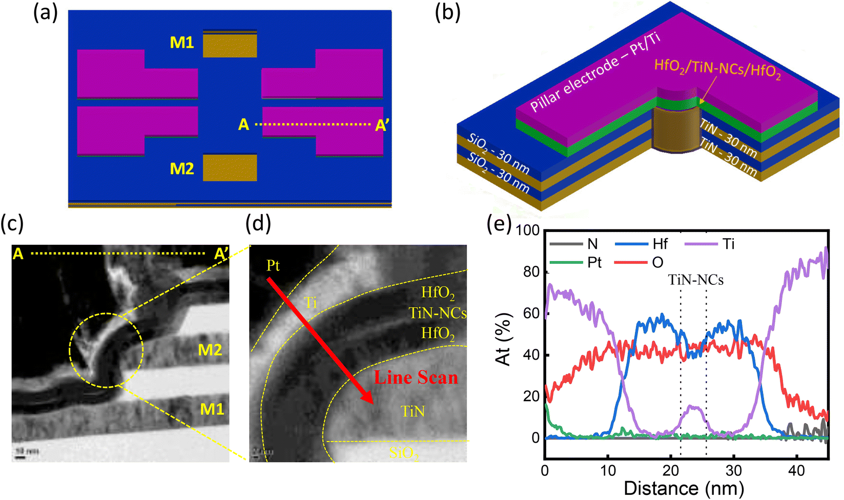 | ||
| Fig. 1 3D schematic diagram of 4 × 2 × 2 vertical resistive random-access memory (VRRAM): (a) top view and (b) bird's eye view. (c) Cross-sectional TEM image and (d) enlarged switching area of Pt/Ti/HfOx/TiN-NCs/HfOx/TiN VRRAM (red line: EDS line scan). (e) Energy-dispersive spectroscopy (EDS) line analysis of VRRAM cells. | ||
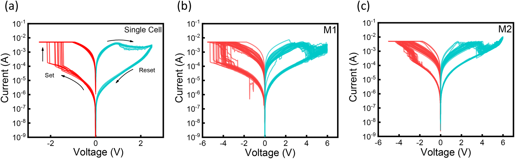
First, we investigated a 2D planar RRAM device with a cell area of 10![[thin space (1/6-em)]](https://www.rsc.org/images/entities/char_2009.gif) 000 μm2 in the same stack as the VRRAM devices. To initiate a switching operation in memristor devices after forming localized conductive filaments, a forming process is required before resistive switching. Fig. 2(a) displays the I–V characteristics of a 2D single cell of Pt/HfOx/TiN-NCs/HfOx/TiN, while the forming curve is presented in Fig. S3(a).† The current increased abruptly at −8.8 V when −10 V of forming voltage was applied to the TE while maintaining a current restriction of 10 μA, creating a conductive filament in the initial state. The oxygen ions moved to the TE and disrupted the conductive path consisting of oxygen vacancies when an opposite voltage of 2.5 V was applied to the TE. During the set process, a negative voltage was applied to reconnect the conductive path for programming under a compliance current of 5 mA, which prevented a permanent breakdown. Typical abrupt set and gradual reset behaviors were observed during the formation and rupture of the filaments at the TiN nanocrystal's interface in DC sweep mode.
000 μm2 in the same stack as the VRRAM devices. To initiate a switching operation in memristor devices after forming localized conductive filaments, a forming process is required before resistive switching. Fig. 2(a) displays the I–V characteristics of a 2D single cell of Pt/HfOx/TiN-NCs/HfOx/TiN, while the forming curve is presented in Fig. S3(a).† The current increased abruptly at −8.8 V when −10 V of forming voltage was applied to the TE while maintaining a current restriction of 10 μA, creating a conductive filament in the initial state. The oxygen ions moved to the TE and disrupted the conductive path consisting of oxygen vacancies when an opposite voltage of 2.5 V was applied to the TE. During the set process, a negative voltage was applied to reconnect the conductive path for programming under a compliance current of 5 mA, which prevented a permanent breakdown. Typical abrupt set and gradual reset behaviors were observed during the formation and rupture of the filaments at the TiN nanocrystal's interface in DC sweep mode.
 | ||
| Fig. 2 I–V characteristics: (a) a single cell, (b) on the first floor (M1), and (c) on the second floor (M2) of VRRAM. | ||
The electrical properties for 30 cycles in two layers of a 3D vertical RRAM are presented in Fig. 2(b) and (c). Fig. S3(b) and (c)† illustrate the forming process, which is necessary (similar to the 2D single cell). We observed that the current of the memory cell on M1 surged quickly at −42.7 V when −50 V was applied to the pillar electrode under the same compliance current of 10 μA as a single cell. In the case of M2, the current increased at −20.2 V to generate an initial conductive path. As the thickness of HfOx increases, numerous associated studies have reported that the forming voltage also increases.50–52 Accordingly, it followed that a higher forming voltage was required for the HfOx switching layer, which had a total thickness of 20 nm.50–52 In addition to the HfOx thickness, the cell area is a factor when determining the forming voltage, because a higher forming voltage is required as the cell area diminishes.26,52 A vertically stacked structure with a cell size of 1.88 μm2 requires a higher forming voltage. The decrease in the forming voltage of M2 after the switching operation of the cell with M1 as the BE could be affected by the interlayer interference effect, which would inevitably be caused by the strong forming voltage related to the structure sharing the pillar electrode and the switching layer. Applying an opposite polarity voltage would disconnect the conductive path composed of oxygen vacancies, similar to the switching behaviors in single cells. We examined 30 consecutive I–V cycles of the memory cells for M1 and M2. When a set voltage of −6.5 V was applied to the pillar electrode, the current increased, which means that a filament was formed in the HfOx layer. During the reset process, the low-resistance state (LRS) was transformed into a high-resistance state (HRS) when 6.5 V was applied, which was similar to the resistive switching behavior in the single cell (both M1 and M2 of VRRAM). The power comparison needed to sustain a low resistance state is shown in Fig. S4.† When compared to a single cell with a 2D planner structure, VRRAM consumes four times less power. Low-power driving is feasible in the vertical-stacked architecture since programming/erasing procedures also use less energy (Fig. S5†).51,52 The RRAM device suffered from severe fluctuations in the operating voltage and resistance states due to the stochastic rupture and regrowth of the branched conductive filaments.16,44 Furthermore, process variations (such as trench hole etching) and the stage of generating multilayer cells in VRRAM are inevitable.22 Accordingly, process variations both within and between layers should be considered. The operating voltage and resistance states were compared depending on the specific design modifications from a single cell of the planetary structure to VRRAM. The distributions of the set voltage for a single cell device and M1 and M2 devices are shown in Fig. 3(a)–(c). The set voltage of the single cell was −1.2 V, compared to −4.26 and −3.82 V for M1 and M2 of VRRAM, respectively. A higher voltage (−3.82 or −4.26 V) in VRRAM was necessary for the formation of a filament due to a decrease in the number of defects because of the cell area reduction.53,54 The set voltage at M1 and M2 differed slightly, which could be attributed to either interlayer interference or process variations within each layer.
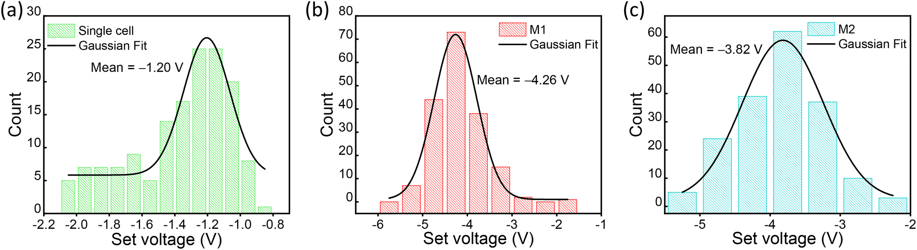 | ||
| Fig. 3 Voltage distribution in the set process for (a) a single cell, (b) the first floor (M1), and (c) the second floor (M2). | ||
Next, the overall cycle-to-cycle resistance state fluctuations and variations from cell-to-cell to device-to-device were collected. Fig. 4(a) and (b) display the LRS and HRS distributions in the M1 and M2 cells of the VRRAM device. All cells were switched under the same voltage and current limit conditions during the set process. The resistance value from each cell was derived from 30 DC cycles when examining the resistance state distribution within a device. The average was divided by the standard deviation to obtain the coefficient of variation (CV) for technically uniform switching. The CVLRS and CVHRS values were 0.41 and 0.49, respectively, in the M1 cell. In comparison, the values of M2 cells were 0.39 and 0.40 for CVLRS and CVHRS, respectively. This result indicated that the LRS and HRS values of the cells sharing the same plane electrode were nearly constant. The conductive filaments connecting the pillar electrode and the plane electrode allowed current to flow near the TiN nanocrystal, enabling stable resistive switching.44,47,48,55–57 Fig. S6† shows cell-to-cell variation in other devices, which shows a similar tendency to Fig. 4(a) and (b). The resistance distribution in five other single cells is shown in Fig. 4c. The coefficients of variation for LRS and HRS in a single cell are 1.05 and 0.54, respectively. The HRS and LRS resistance distribution of fifteen VRRAM devices are displayed to demonstrate device-to-device variability in Fig. 4(d). In the M1 cell, the CVLRS and CVHRS values were 0.87 and 0.93, respectively, and in the M2 cell, the CVLRS and CVHRS values were 3.13 and 1.76. As can be seen, the coefficient of variation is greater at M2 than at M1, and the reason why the coefficient of variation is relatively high at M2 is that the strong forming voltage of M1 affects the resistance state of the cells located at M2. The CV value is also increased by a cycle that does not have a high current level and has an intermediate resistance value but typically has a constant resistance value in 15 different devices. By enhancing the stochastic features of filament generation in a thick HfOx switching layer with a thickness of 20 nm, a stable resistance state could be maintained in terms of cycle-to-cycle and device-to-device.
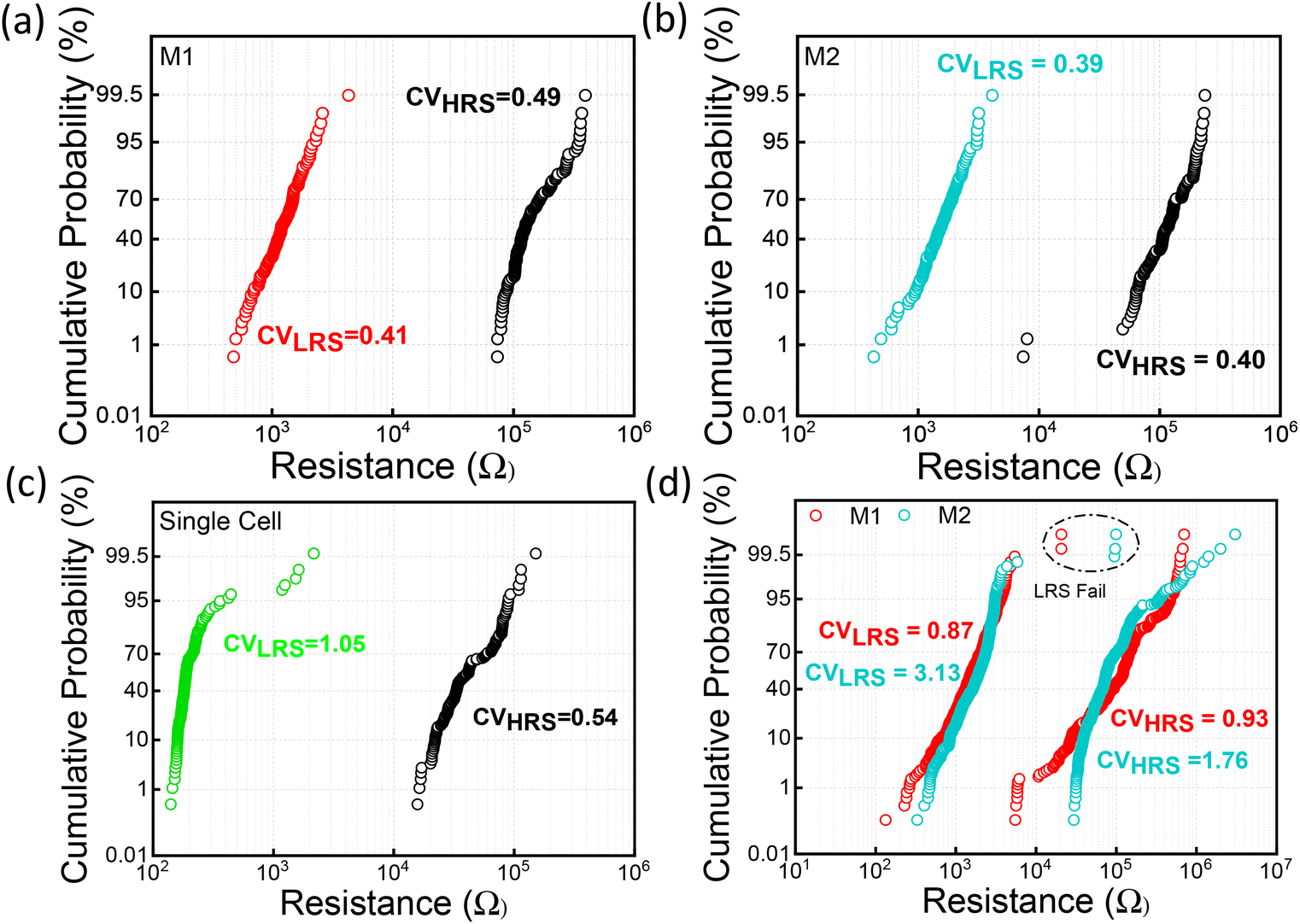 | ||
| Fig. 4 Variation of the resistance parameters of four different cells within a device (a) on the first floor (M1) and (b) on the second floor (M2) from 30 consecutive cycles, and (c) five cells in a 2D single cell. (d) The resistance state the cumulative probability of fifteen devices of VRRAM (M1 and M2). | ||
Stable endurance is important in memory or synaptic device performances for evaluating reliability and reproduction.58Fig. 5(a) displays the single-cell endurance properties for up to 1000 cycles. The device exhibited stable endurance characteristics with an on/off ratio of approximately 110. Similarly, in VRRAM, the repetition in DC mode could be conducted while maintaining an on/off ratio of approximately 60 (M1) and 75 (M2) for 500 cycles, as displayed in Fig. 5(b) and (c). Moreover, a retention test at a read voltage of 0.2 V was conducted, as displayed in Fig. 5(d)–(f). For nonvolatile memory applications, single cells (Fig. 5(d)), M1 (Fig. 5(e)), and M2 (Fig. 5(f)) all demonstrated outstanding retention characteristics of 10000 s without any overlap or degradation. Fig. 5(g) and (h) depict a comparison of the pulse endurance properties in a single cell, M1 and M2 in VRRAM and the resistance state conversion was observed when a 0.2 V/100 μs read pulse was applied. In the case of a single cell, set/reset pulses of −1.4 V/100 μs and 2 V/100 μs were utilized. VRRAM, M1, and M2 were also tested with −3.2 V/100 μs set pulses and 4 V/100 μs reset pulses. In all three instances, the cycle was run more than 10000 times, demonstrating the stable endurance properties in AC mode.
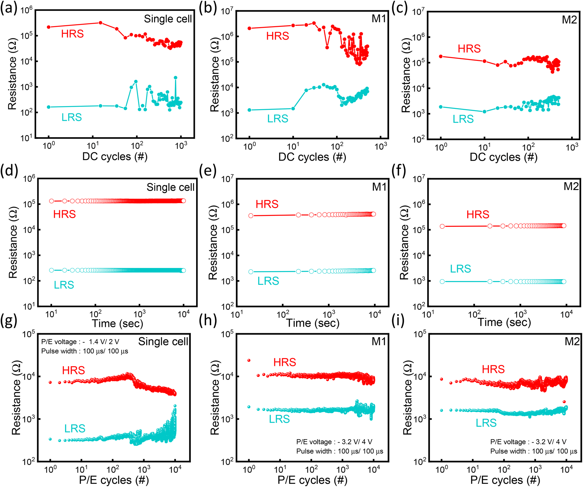 | ||
| Fig. 5 Endurance characteristics of Pt/Ti/HfOx/TiN-NCs/HfOx/TiN for (a) a single cell, (b) the first floor (M1), and (c) the second floor (M2) in the HRS and LRS. Retention of three samples measured for 10000 s: (d) a single cell, (e) M1, and (f) M2 in the HRS and LRS measured at 0.2 V. Pulse endurance: (g) a single cell, (h) M1, and (i) M2. | ||
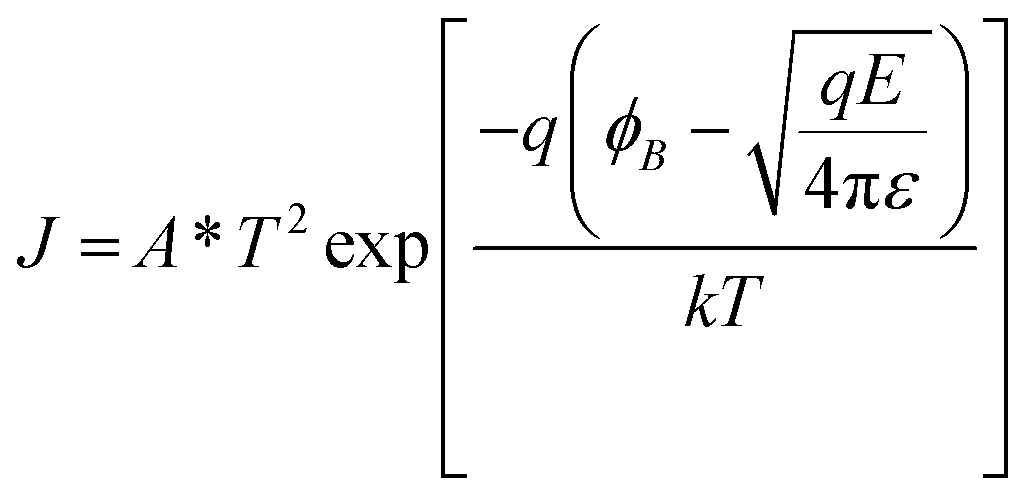
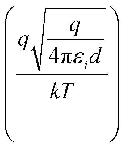
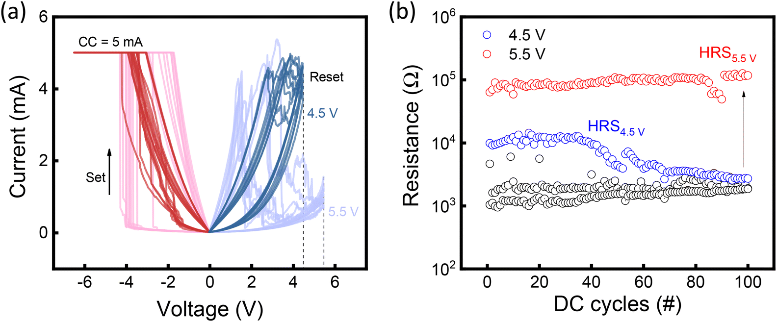
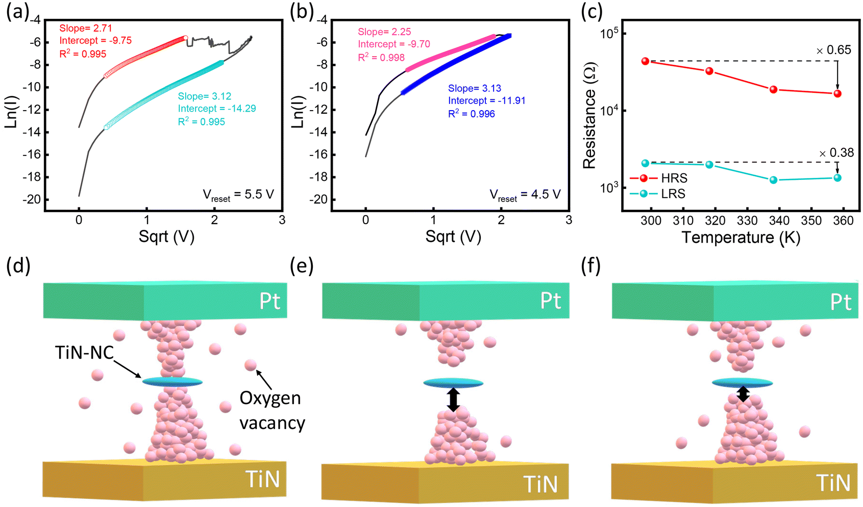
To overcome the limitations of binary memory, which can only store the two states of 0 and 1 for neuromorphic application, MLC for implementing multiple synaptic weights are crucial.59–62 Generally, MLC are achieved by adjusting the reset voltage or compliance current in the set and reset processes. Fig. 6(a) displays the I–V characteristics when two different reset voltages were applied: 4.5 and 5.5 V. When the reset voltage was increased from 4.5 to 5.5 V, the on/off ratio increased and the electric field boosting filament oxidation strengthened, resulting in a higher resistance state. The DC endurance properties of 100 cycles for the two reset voltage conditions are displayed in Fig. 6(b). When a smaller reset voltage was applied, the filament was not totally ruptured as more switching was repeated. However, when a stronger reset voltage was applied, the conductive path was completely disconnected, resulting in 100-cycle achievement. Fig. S7† illustrates the I–V characteristics with fixed set and reset voltages along with different compliance currents of 500 μA, 1 mA, and 5 mA. Here, the VRRAM device with TiN nanocrystals was not suitable for executing MLC by changing the diameter of the CF through compliance current adjustment, since the LRS tended to be constant as the compliance current increased. As a result, the multilevel resistance state could be established by setting an appropriate reset voltage, suggesting that RRAM is capable of multilevel storing and is appropriate for synaptic devices. Next, the conduction mechanism of 3D VRRAM with TiN nanocrystals was investigated. Fig. 7(a) and (b) display the fitting of the I–V curve for reset voltages of 5.5 and 4.5 V, respectively. For both HRS and LRS, ln(I) was proportional to  , which indicated that regardless of the reset voltage, both resistance states followed Schottky emission that was established at the interface between the metal electrode and the switching layer. The barrier was overcome by electrons or holes with thermal energy.63 Schottky emission is represented by the following eqn (1):
 | (1) |
 | (2) |
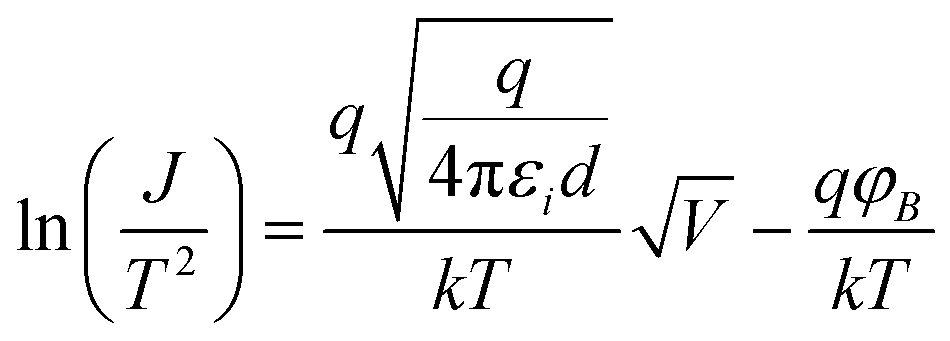
 is the slope value and
 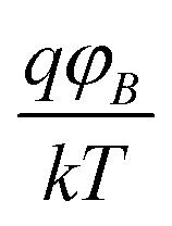 is the intercept of the linear equation.66 As a result, the intercept determines the barrier height and the slope value estimates the Schottky emission distance.67,68 As the reset curve in Fig. 7(a) switched from LRS to HRS, the slope ascended from 2.71 to 3.12 and the intercept's absolute value increased from 9.75 to 14.29. This result indicated that a barrier height reduction occurred due to the conduction of electrons across the potential energy barrier at the interface.69 When a reset voltage of 4.5 V was applied, the reset curve was fitted as shown in Fig. 7(b). The absolute value of the intercept increased from 11.91 to 14.29 when the reset voltage was increased, and the increased barrier height suppressed electrons from moving across the barrier.
 | ||
| Fig. 6 Multilevel characteristics of Pt/Ti/HfOx/TiN-NCs/HfOx/TiN VRRAM: (a) DC switching I–V curves and (b) DC endurance (100 repeated sweeps). | ||
 | ||
| Fig. 7 Current fitting of the HRS and LRS with different reset voltages: (a) 5.5 V and (b) 4.5 V. (c) Temperature dependence of the resistance state. Schematic diagram illustrating the conduction mechanism: (d) set process and multilevel switching process mechanism with reset voltages of (e) 5.5 V and (f) 4.5 V. | ||
Fig. 7(c) displays the resistance values as a function of temperature. Here, both resistance states decreased as the temperature increased. The devices with TiN nanocrystals followed the Schottky emission conduction mechanism, which indicated an increase in the number of electrons thermally passing through the barrier as the temperature increased. The conduction process of VRRAM with TiN nanocrystals is schematically shown in Fig. 7(d)–(f). The TEM image in Fig. S8† illustrates how the filament is attached and disconnected in VRRAM. For the transition from HRS to LRS, a negative voltage induced a conductive path consisting of oxygen vacancies near the TiN nanocrystal interface (Fig. 7(d)). Fig. 7(e) illustrates the reset process at 5.5 V, which resulted in a higher potential barrier height near the TiN nanocrystal interface compared to 4.5 V. This result implied that the gap between the TiN-NCs and the conductive filaments was larger at 5.5 V, resulting in a higher resistance state.
Various analyses of pulse responses were conducted to assess the synaptic behaviors of the devices, which mimic the basic biological synapse functions. Long-term potentiation (LTP) and long-term depression (LTD) properties are the most fundamentally necessary functions among the essential synaptic functions.70–72 Receiving stimulus impulses can strengthen the connection between two adjacent neurons, resulting in potentiation or depression.70–72 To simulate the LTD and LTP properties, a conductance change that was constantly altered by applying a pulse signal was examined. Potentiation and depression characteristics under 50 identical pulses of the same amplitude and width were evaluated, in which the conductance was converted from the current at a read voltage of 0.2 V, as displayed in Fig. 8(a). The conductance was increased by applying an identical pulse of −3 V/10 μs for the LTP behavior. To represent the LTD behavior, 50 consecutive pulses with a pulse height of 3 V and a pulse width of 10 μs were employed. Binary switching renders it more difficult to imitate an analog synapse operation since the conductance changes quickly in the first pulse signal. For more gradual conductance change modulation, potentiation was obtained by using pulse voltage changes from −1.7 to −2.18 V in steps of 0.01 V with a pulse width of 10 μs, while depression was obtained by changing the pulse voltage from 1.8 to 2.17 V in steps of −0.01 V at a fixed pulse width (10 μs) with a read voltage of 0.2 V (Fig. 8(b)). The conductance progressively increased in accordance with the potentiation pulse sequence when the incremental pulse was applied, and then gradually decreased for the depression pulse. The following pulse modification method can be used to achieve a linear conductance change.
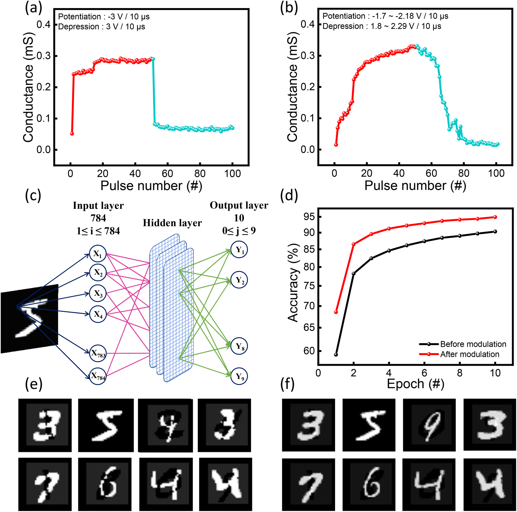 | ||
| Fig. 8 (a) Conductance states produced by identical set (−3 V/10 μs) and reset (3 V/10 μs) pulses during potentiation and depression. (b) Optimized conductance states stimulated by trains of incremental pulses (potentiation: −1.7 to −2.18 V/10 μs, depression: [1.8 to 2.29 V/10 μs]. For pattern recognition simulation: (c) schematic of the neural network framework. (d) Training results of before and after pulse modulation (incremental pulse scheme). Output images of each pulse: (e) identical and (f) incremental pulse. | ||
To demonstrate the improved results for neuromorphic systems, a pattern recognition simulation was performed. A neural network system for evaluating the potentiation and depression properties was constructed to determine its suitability for pattern recognition. A deep neural network (DNN) structure was developed utilizing the Modified National Institute of Standards and Technology (MNIST) database, as shown in Fig. 8(c). The number of input nodes used was 784, which corresponded to the number of pixels in the MNIST binary images, and a sample image of size 28 × 28 pixels was employed. The input data were transmitted to the output layer after a nonlinear transformation has been performed in the three hidden layers between the input and output layers while considering the weight parameter. The outcome was provided by the output layer in 10 nodes, corresponding to 0–9. The measured conductance values were then used as the artificial weights in a neural network. Fig. 8(d) displays a comparison of the recognition accuracy based on the data measured in Fig. 8(a) and (b) using the aforementioned method. Fig. 8(e) and (f) display the images in which 60000 images were acquired over a total of 10 epochs from the measurement results obtained with an identical and incremental pulse, respectively. The identical pulse scheme yielded a recognition accuracy of 90.32%, whereas the recognition accuracy of the pulse modulation scheme was recorded as 94.91%. The linear conductance change proved to be suitable for neuromorphic applications, as the recognition accuracy could be boosted to 4.59% by incremental pulse modulation.
Fig. 9(a) illustrates the synapse junction structure that allowed a stimulus to be transmitted from one neuron to another between two adjacent neurons. Here, the calcium channel opened at the previous synaptic terminal and transferred to the chemical synapse in response to the initial stimulation. To trigger postsynaptic neurons, neurotransmitters were then released and dispersed into synaptic neurons.73,74 In the following, the ways that stimuli are transferred in chemical synapses are discussed, where two-terminal RRAM works in a way that is both physically and functionally equivalent.75 The method of sending a spike pulse to the TE and verifying a response at the BE to replicate synaptic characteristics in a two-terminal plane RRAM has been actively researched.76 We additionally employed vertical RRAM in 3D to accomplish similar synaptic plasticity properties. In neuromorphic systems that mimic the human brain, synaptic plasticity refers to non-volatile changes in the synaptic weight.77–79 To vary the synaptic weight between pre- and post-neurons, the interval time and strength of the spiking signal are changed.78–80
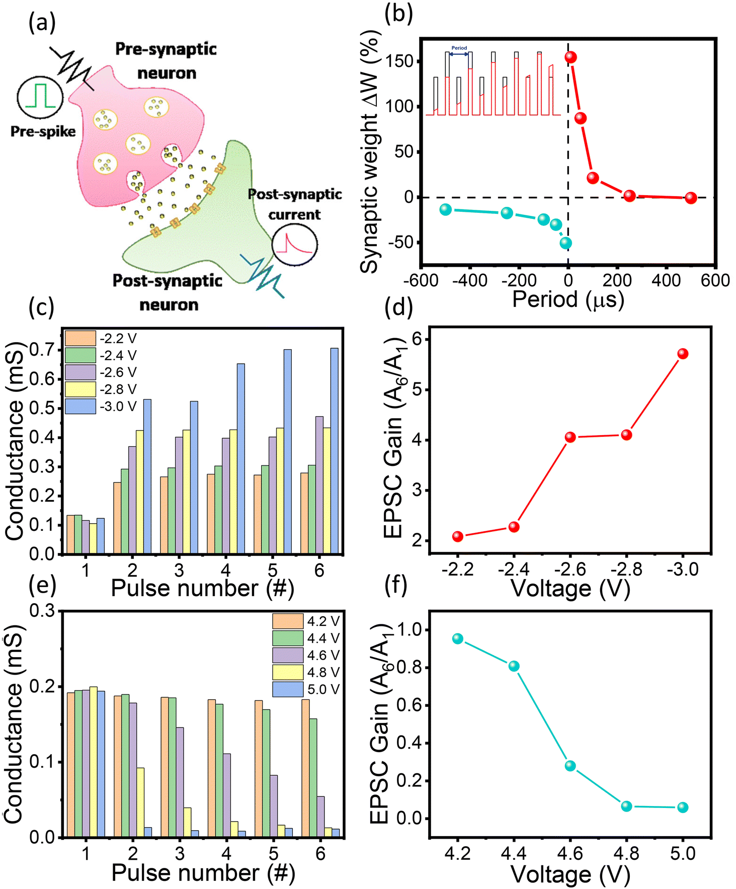 | ||
| Fig. 9 (a) Conceptual diagram of a biological synapse structure. Synaptic plasticity emulation of 3D VRRAM: (b) Experimental demonstration of excitatory post-synaptic current (EPSC) with different interval times. (c) Conductance response of the memristor for programming pulse trains with different pulse heights, (d) EPSC gain (A6/A1) at different pulse voltages from −2.2 to −3 V/10 μs. (e) Conductance changes of EPSC varying the erasing spike amplitude. (f) EPSC gain from 4.2 to 5 V/10 μs. | ||
Excitatory post-synaptic current (EPSC) measurements of spike-rate-dependent plasticity (SRDP) are displayed in Fig. 9(b). By varying the interval time between pulses to 10, 50, 100, 250, and 500 μs, the rate of five identical programming or erase pulses were altered with a programming pulse of −2.4 V/10 μs and an erase pulse of 2.7 V/10 μs. The stimulus transmitted to the postsynaptic neuron was stronger at higher frequencies (shorter periods). Additionally, the post-synaptic response changed as the strength of the stimulus varied, as evidenced in Fig. 9(c)–(f). Using the same five programming or erase pulses of varying amplitudes and a read voltage of 0.2 V applied between each pulse, the conductance value was measured with the interval time fixed. The conductance value before applying a programming pulse was represented by pulse number 1, and after applying a programming pulse train was represented by pulse number 6, as displayed in Fig. 9(c). Fig. 9(d) depicts the EPSC gain as the ratio of the current to the initial state after the application of five programming pulses. When the EPSC gain was represented by the conductance value in Fig. 9(c), the EPSC gain correspondingly increased in proportion to the amplitude of the programming pulse. Fig. 9(e) indicates the post-synaptic response for the applied erase pulse when the erase pulse amplitude was altered. Here, the EPSC gain reduced with increasing erase pulse amplitude in Fig. 9(f), demonstrating that post-synaptic neurons’ responses (which vary with the stimulus intensity) can convincingly replicate synaptic properties.
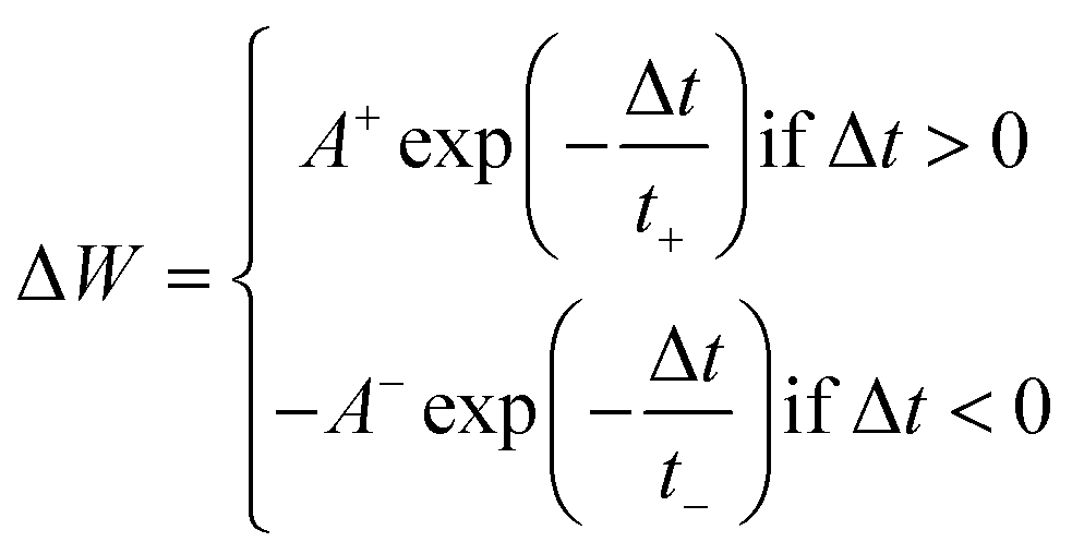
Fig. 10 displays the spike-timing dependent plasticity (STDP), which determines the synaptic weight based on how long it takes for the pre-neuron stimulus to reach the post-neuron.73 The framework displayed in Fig. 10(a) controlled the strength of the connections between the neurons and then converted to long-term memory or removed data by strengthening or weakening these links. The pre- and post-spikes were applied to an identical pulse train (−1, +2.5, +2.3, +2.1, +1.9, +1.7, and +1.5 V) and the pulse interval for each pulse was 10 μs. While LTD occurred when the post-synaptic pulse was before the pre-synaptic pulse, LTP occurred when the pre-synaptic pulse reached before the latter. In both cases, as the interval between the pre- and post-synaptic spikes lengthened, the change in the synaptic weight declined. Fig. 10(b) displays the synaptic weight change (ΔW = (Gt − Gi)/Gi × 100%) for spiking timing (Δt), with the red fitting curve corresponding to the synaptic change function using the following eqn (2):
 | (3) |
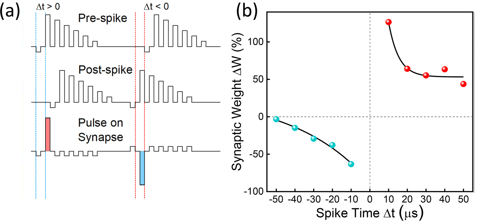 | ||
| Fig. 10 (a) Pulse scheme for pre-spike, post-spike, and effective pulse on synapses. (b) Spike-timing-dependent plasticity (STDP) behaviors of Pt/Ti/HfOx/TiN-NCs/HfOx/TiN VRRAM. | ||
Herein, we fabricated a Pt/Ti/HfOx/TiN-NCs/HfOx/TiN vertical RRAM structure and evaluated the resistive switching properties for use as high-density neuromorphic synapses. The process from trench etching to pillar electrode deposition proceeded successfully and outstanding non-volatile properties were achieved. This was verified by measurements of the excellent memory characteristics of I–V curves, retention, and DC endurance at each layer. Cycle-to-cycle, cell-to-cell, and device-to-device variations were also examined based on the distribution of driving voltage and resistance in single cells of the planar structure and each layer of VRRAM with NCs. As the cell size was minimized due to the 3D configuration, the LRS of a single cell was lower than that of VRRAM, which suggested that the required driving voltage increased or that the structure sharing the switching layer with the pillar electrode would be affected. In the pattern recognition simulations, the recognition accuracy was improved by linearly designing conductance changes using the pulse amplitude modulation of binary switching that flipped between two states (LRS and HRS). Additionally, TiN-NC inserted VRRAM shows promising biological synapse features like potentiation and depression, SRDP, and STDP in addition to the multilayer characteristics accomplished through reset voltage regulation. Thus, 3D VRRAM with TiN-NCs is a promising candidate for neuromorphic computing systems as artificial synapses and data storage.
Conflicts of interest
There are no conflicts to declare.Acknowledgements
This research was supported by the National R&D Program through the National Research Foundation of Korea (NRF) funded by the Ministry of Science and ICT under Grants 2020M3F3A2A01082593 and 2021M3F3A2A01037927.References
- Y. Huang, Y. Gu, X. Wu, R. Ge, Y. F. Chang, X. Wang, J. Zhang, D. Akinwande and J. C. Lee, Front. nanotechnol., 2021, 3, 782836 CrossRef.
- A. D. Malony , ACM Digital Library and Sigarch, Proceedings of the 27th international ACM conference on International conference on supercomputing, ACM, 2013.
- F. Zahoor, T. Z. Azni Zulkifli and F. A. Khanday, Nanoscale Res. Lett., 2020, 15, 90 CrossRef CAS PubMed.
- A. Goda and K. Parat, in Technical Digest - International Electron Devices Meeting, IEDM, 2012.
- 2007 Symposium on VLSI Technology: digest of technical papers: June 12-14, 2007: Kyoto, Japan, IEEE Xplore, 2007.
- C. S. Hwang, Adv. Electron. Mater., 2015, 1(6), 1400056 CrossRef.
- K. T. Park, S. Nam, D. Kim, P. Kwak, D. Lee, Y. H. Choi, M. H. Choi, D. H. Kwak, D. H. Kim, M. S. Kim, H. W. Park, S. W. Shim, K. M. Kang, S. W. Park, K. Lee, H. J. Yoon, K. Ko, D. K. Shim, Y. Lo Ahn, J. Ryu, D. Kim, K. Yun, J. Kwon, S. Shin, D. S. Byeon, K. Choi, J. M. Han, K. H. Kyung, J. H. Choi and K. Kim, IEEE J. Solid-State Circuits, 2015, 50, 204–213 Search PubMed.
- T. Kgil, D. Roberts and T. Mudge, in Proceedings - International Symposium on Computer Architecture, 2008, pp. 327–338.
- J. Lee, J. Jang, J. Lim, Y. G. Shin, K. Lee and E. Jung, in Technical Digest - International Electron Devices Meeting, IEDM, Institute of Electrical and Electronics Engineers Inc., 2017, pp. 11.2.1–11.2.4.
- S. S. Kim, S. K. Yong, W. Kim, S. Kang, H. W. Park, K. J. Yoon, D. S. Sheen, S. Lee and C. S. Hwang, Adv. Mater., 2022, 2200659 CrossRef PubMed.
- G. H. Lee, S. Hwang, J. Yu and H. Kim, Appl. Sci., 2021, 11(15), 6703 CrossRef CAS.
- K. M. Persson, M. S. Ram and L. E. Wernersson, IEEE J. Electron Devices Soc., 2021, 9, 564–569 CAS.
- B. J. Choi, A. C. Torrezan, J. P. Strachan, P. G. Kotula, A. J. Lohn, M. J. Marinella, Z. Li, R. S. Williams and J. J. Yang, Adv. Funct. Mater., 2016, 26, 5290–5296 CrossRef CAS.
- S. Kim, H. Kim, S. Hwang, M. H. Kim, Y. F. Chang and B. G. Park, ACS Appl. Mater. Interfaces, 2017, 9, 40420–40427 CrossRef CAS PubMed.
- G. Ding, S.-T. Han, C.-C. Kuo, V. A. L. Roy and Y. Zhou, Small Struct., 2023, 4, 2200150 CrossRef CAS.
- X. Lian, M. Wang, M. Rao, P. Yan, J. J. Yang and F. Miao, Appl. Phys. Lett., 2017, 110(17) DOI:10.1063/1.4982593.
- B. Hudec, C. W. Hsu, I. T. Wang, W. L. Lai, C. C. Chang, T. Wang, K. Fröhlich, C. H. Ho, C. H. Lin and T. H. Hou, Sci. China Inform. Sci., 2016, 59, 1–21 Search PubMed.
- G. W. Burr, R. S. Shenoy, K. Virwani, P. Narayanan, A. Padilla, B. Kurdi and H. Hwang, J. Vac. Sci. Technol., B: Nanotechnol. Microelectron.: Mater., Process., Meas., Phenom., 2014, 32, 040802 Search PubMed.
- Y. Deng, H. Y. Chen, B. Gao, S. Yu, S. C. Wu, L. Zhao, B. Chen, Z. Jiang, X. Liu, T. H. Hou, Y. Nishi, J. Kang and H. S. P. Wong, in Technical Digest - International Electron Devices Meeting, IEDM, 2013.
- D. Ielmini, IEEE Trans. Electron Devices, 2011, 58, 4309–4317 CAS.
- L. Zhang, S. Cosemans, D. J. Wouters, B. Govoreanu, G. Groeseneken and M. Jurczak, in 2013 5th IEEE International Memory Workshop, IMW 2013, 2013, pp. 155–158.
- J. Park, T. H. Kim, O. Kwon, M. Ismail, C. Mahata, Y. Kim, S. Kim and S. Kim, Nano Energy, 2022, 104, 107886 CrossRef CAS.
- J. Y. Seok, S. J. Song, J. H. Yoon, K. J. Yoon, T. H. Park, D. E. Kwon, H. Lim, G. H. Kim, D. S. Jeong and C. S. Hwang, Adv. Funct. Mater., 2014, 24, 5316–5339 CrossRef CAS.
- S. H. Jo, T. Kumar, S. Narayanan, W. D. Lu and H. Nazarian, in Technical Digest - International Electron Devices Meeting, IEDM, Institute of Electrical and Electronics Engineers Inc., 2015, vol. 2015-February, pp. 6.7.1–6.7.4.
- L. Gao, Q. Ren, J. Sun, S. T. Han and Y. Zhou, J. Mater. Chem. C, 2021, 9, 16859–16884 RSC.
- A. Napolean, N. M. Sivamangai, S. Rajesh, R. NaveenKumar, N. Nithya, S. Kamalnath and N. Aswathy, Emergent Mater., 2022, 5, 489–508 CrossRef.
- K. C. Chuang, C. Y. Chu, H. X. Zhang, J. D. Luo, W. S. Li, Y. S. Li and H. C. Cheng, IEEE J. Electron Devices Soc., 2019, 7, 589–595 CAS.
- C. Li, F. Wang, K. Hu, W. Li, J. Zhao, T. Ren, Z. Song and K. Zhang, J. Phys. D: Appl. Phys., 2020, 53(33), 335104 CrossRef CAS.
- W. U. Wenjuan, Study of Tao X-based resistive random access memory, 2012 Search PubMed.
- L. Chen, T. Y. Wang, Y. W. Dai, M. Y. Cha, H. Zhu, Q. Q. Sun, S. J. Ding, P. Zhou, L. Chua and D. W. Zhang, Nanoscale, 2018, 10, 15826–15833 RSC.
- D. C. Kim, S. Seo, S. E. Ahn, D. S. Suh, M. J. Lee, B. H. Park, I. K. Yoo, I. G. Baek, H. J. Kim, E. K. Yim, J. E. Lee, S. O. Park, H. S. Kim, U. I. Chung, J. T. Moon and B. I. Ryu, Appl. Phys. Lett., 2005, 87(23) DOI:10.1063/1.2204649.
- J. Robertson, EPJ Appl. Phys., 2004, 28, 265–291 CrossRef CAS.
- S. Spiga, F. Driussi, G. Congedo, C. Wiemer, A. Lamperti and E. Cianci, ACS Appl. Nano Mater., 2018, 1, 4633–4641 CrossRef CAS.
- D. Ielmini , in Technical Digest - International Electron Devices Meeting, IEDM, 2011.
- S. Ambrogio, S. Balatti, A. Cubeta, A. Calderoni, N. Ramaswamy and D. Ielmini, IEEE Trans. Electron Devices, 2014, 61, 2912–2919 CAS.
- M. Trapatseli, A. Khiat, S. Cortese, A. Serb, D. Carta and T. Prodromakis, J. Appl. Phys., 2016, 120(2) DOI:10.1063/1.4958672.
- N. Vasileiadis, P. Karakolis, P. Mandylas, V. Ioannou-Sougleridis, P. Normand, M. Perego, P. Komninou, V. Ntinas, I. A. Fyrigos, I. Karafyllidis, G. C. Sirakoulis and P. Dimitrakis, IEEE Trans. Nanotechnol., 2021, 20, 356–364 CAS.
- K. P. Min, C. Y. Li, T. J. Chang and S. Y. Chu, ACS Appl. Electron. Mater., 2021, 3, 5327–5334 CrossRef CAS.
- F. Hussain, M. Imran, R. M. A. Khalil, M. A. Sattar, N. A. Niaz, A. M. Rana, M. Ismail, E. A. Khera, U. Rasheed, F. Mumtaz, T. Javed and S. Kim, Vacuum, 2019, 168, 108842 CrossRef CAS.
- Q. Wang, G. Niu, S. Roy, Y. Wang, Y. Zhang, H. Wu, S. Zhai, W. Bai, P. Shi, S. Song, Z. Song, Y. H. Xie, Z. G. Ye, C. Wenger, X. Meng and W. Ren, J. Mater. Chem. C, 2019, 7, 12682–12687 RSC.
- C. Mahata, M. Kang and S. Kim, Nanomaterials, 2020, 10, 1–12 CrossRef PubMed.
- J. Lin, S. Wang and H. Liu, Electronics, 2021, 10, 1–10 Search PubMed.
- J. Woo, K. Moon, J. Song, S. Lee, M. Kwak, J. Park and H. Hwang, IEEE Electron Device Lett., 2016, 37, 994–997 CAS.
- G. S. Park, Y. B. Kim, S. Y. Park, X. S. Li, S. Heo, M. J. Lee, M. Chang, J. H. Kwon, M. Kim, U. I. Chung, R. Dittmann, R. Waser and K. Kim, Nat. Commun., 2013, 4(1), 2382 CrossRef PubMed.
- J. Shang, W. Xue, Z. Ji, G. Liu, X. Niu, X. Yi, L. Pan, Q. Zhan, X. H. Xu and R. W. Li, Nanoscale, 2017, 9, 7037–7046 RSC.
- M. Tsigkourakos, P. Bousoulas, V. Aslanidis, E. Skotadis and D. Tsoukalas, Phys. Status Solidi A, 2017, 214(12), 1700570 CrossRef.
- W. Banerjee and S. Maikap, in International Symposium on VLSI Technology, Systems, and Applications, Proceedings, 2012.
- C. Mahata, M. Ismail, M. Kang and S. Kim, Nanoscale Res. Lett., 2022, 17(1), 58 CrossRef CAS PubMed.
- C. Mahata and S. Kim, Chaos, Solitons Fractals, 2021, 153, 111518 CrossRef.
- D. T. Wang, Y. W. Dai, J. Xu, L. Chen, Q. Q. Sun, P. Zhou, P. F. Wang, S. J. Ding and D. W. Zhang, IEEE Electron Device Lett., 2016, 37, 878–881 CAS.
- Z. Zhang, F. Wang, K. Hu, Y. She, S. Song, Z. Song and K. Zhang, Materials, 2021, 14(12), 3330 CrossRef CAS PubMed.
- S. Choi, W. Sun and H. Shin, IEEE J. Electron Devices Soc., 2018, 6, 1192–1196 CAS.
- N. Raghavan, A. Fantini, R. Degraeve, P. J. Roussel, L. Goux, B. Govoreanu, D. J. Wouters, G. Groeseneken and M. Jurczak, Microelectron. Eng., 2013, 109, 177–181 CrossRef CAS.
- J. Lee, J. Park, S. Jung and H. Hwang, in 2011 IEEE International Interconnect Technology Conference and 2011 Materials for Advanced Metallization, IITC/MAM 2011, 2011.
- B. Govoreanu, G. S. Kar, Y. Y. Chen, V. Paraschiv, S. Kubicek, A. Fantini, I. P. Radu, L. Goux, S. Clima, R. Degraeve, N. Jossart, O. Richard, T. Vandeweyer, K. Seo, P. Hendrickx, G. Pourtois, H. Bender, L. Altimime, D. J. Wouters, J. A. Kittl and M. Jurczak, in Technical Digest - International Electron Devices Meeting, IEDM, 2011.
- L. Chen, H. Y. Gou, Q. Q. Sun, P. Zhou, H. L. Lu, P. F. Wang, S. J. Ding and D. Zhang, IEEE Electron Device Lett., 2011, 32, 794–796 CAS.
- Q. Wu, W. Banerjee, J. Cao, Z. Ji, L. Li and M. Liu, Appl. Phys. Lett., 1995, 67(16) DOI:10.1063/1.5030780.
- M. Ismail, C. Mahata, O. Kwon and S. Kim, ACS Appl. Electron. Mater., 2022, 4(3), 1288–1300 CrossRef CAS.
- M. Zhao, B. Gao, J. Tang, H. Qian and H. Wu, Appl. Phys. Rev., 2020, 7(1), 011301 CAS.
- D. Ielmini, Z. Wang and Y. Liu, APL Mater., 2018, 190, 44–53 CAS.
- J. H. Ju, S. Seo, S. Baek, D. Lee, S. Lee, T. Lee, B. Kim, J. J. Lee, J. Koo, H. Choo, S. Lee and J. H. Park, Small, 2021, 17(34), 2102595 CrossRef CAS PubMed.
- Y. Sun, H. Xu, C. Wang, B. Song, H. Liu, Q. Liu, S. Liu and Q. Li, IEEE Electron Device Lett., 2018, 39, 1298–1301 CAS.
- F. C. Chiu, Adv. Mater. Sci. Eng., 2014, 2014, 578168 Search PubMed.
- P. H. Chen, C. Y. Lin, T. C. Chang, J. K. Eshraghian, Y. T. Chao, W. D. Lu and S. M. Sze, ACS Appl. Mater. Interfaces, 2022, 14, 2343–2350 CrossRef CAS PubMed.
- L. Zhang, Z. Xu, J. Han, L. Liu, C. Ye, Y. Zhou, W. Xiong, Y. Liu and G. He, J. Mater. Sci. Technol., 2020, 49, 1–6 CrossRef.
- K. H. Chen, T. M. Tsai, C. M. Cheng, S. J. Huang, K. C. Chang, S. P. Liang and T. F. Young, Materials, 2017, 11(1), 43 CrossRef PubMed.
- R. Zhang, K. C. Chang, T. C. Chang, T. M. Tsai, S. Y. Huang, W. J. Chen, K. H. Chen, J. C. Lou, J. H. Chen, T. F. Young, M. C. Chen, H. L. Chen, S. P. Liang, Y. E. Syu and S. M. Sze, IEEE Electron Device Lett., 2014, 35, 630–632 CAS.
- T. J. Chu, T. M. Tsai, T. C. Chang, K. C. Chang, R. Zhang, K. H. Chen, J. H. Chen, T. F. Young, J. W. Huang, J. C. Lou, M. C. Chen, S. Y. Huang, H. L. Chen, Y. E. Syu, D. Bao and S. M. Life, IEEE Electron Device Lett., 2014, 35, 217–219 CAS.
- C. Ye, T. Deng, J. Zhang, L. Shen, P. He, W. Wei and H. Wang, Semicond. Sci. Technol., 2016, 31(10), 105005 CrossRef.
- H. Yeon, P. Lin, C. Choi, S. H. Tan, Y. Park, D. Lee, J. Lee, F. Xu, B. Gao, H. Wu, H. Qian, Y. Nie, S. Kim and J. Kim, Nat. Nanotechnol., 2020, 15, 574–579 CrossRef CAS PubMed.
- Y. Li, E. J. Fuller, J. D. Sugar, S. Yoo, D. S. Ashby, C. H. Bennett, R. D. Horton, M. S. Bartsch, M. J. Marinella, W. D. Lu and A. A. Talin, Adv. Mater., 2020, 32(45), 2003984 CrossRef CAS PubMed.
- J. Woo and S. Yu, IEEE Nanotechnol. Mag., 2018, 12, 36–44 Search PubMed.
- T. Masquelier, R. Guyonneau and S. J. Thorpe, Neural Comput., 2009, 21, 1259–1276 CrossRef PubMed.
- M. Ziegler, C. Wenger, E. Chicca and H. Kohlstedt, J. Appl. Phys., 2018, 124(15) DOI:10.1063/1.5042040.
- S. R. Zhang, L. Zhou, J. Y. Mao, Y. Ren, J. Q. Yang, G. H. Yang, X. Zhu, S. T. Han, V. A. L. Roy and Y. Zhou, Adv. Mater. Technol, 2019, 4(2), 1800342 CrossRef.
- Z. Shen, C. Zhao, Y. Qi, W. Xu, Y. Liu, I. Z. Mitrovic, L. Yang and C. Zhao, Nanomaterials, 2020, 10, 1–31 Search PubMed.
- J. J. Yang, D. B. Strukov and D. R. Stewart, Nat. Nanotechnol., 2013, 8, 13–24 CrossRef CAS PubMed.
- O. Kapur, D. Guo, J. Reynolds, Y. Han, R. Beanland, L. Jiang, C. H. de Groot and R. Huang, Adv. Electron. Mater., 2022, 8(9), 2200312 CrossRef CAS.
- H. Bian, X. Qin, Y. Wu, Z. Yi, S. Liu, Y. Wang, C. D. S. Brites, L. D. Carlos and X. Liu, Adv. Mater., 2022, 34(25), 2101895 CrossRef CAS PubMed.
- T. Ohno, T. Hasegawa, T. Tsuruoka, K. Terabe, J. K. Gimzewski and M. Aono, Nat. Mater., 2011, 10, 591–595 CrossRef CAS PubMed.
- J.-L. Gaiarsa, O. Caillard and Y. Ben-Ari, Trends Neurosci., 2002, 25(11), 564–570 CrossRef CAS PubMed.
Footnote |
| † Electronic supplementary information (ESI) available. See DOI: https://doi.org/10.1039/d3nr01930f |
| This journal is © The Royal Society of Chemistry 2023 |