
 Open Access Article
 This Open Access Article is licensed under a Creative Commons Attribution-Non Commercial 3.0 Unported Licence
Mechanistic understanding of the interfacial properties of metal–PtSe2 contacts†
Liujian
Qi
 ,
Mengqi
Che
,
Mingxiu
Liu
,
Bin
Wang
,
Nan
Zhang
,
Yuting
Zou
,
Xiaojuan
Sun
,
Zhiming
Shi
,
Dabing
Li
and
Shaojuan
Li
*
,
Mengqi
Che
,
Mingxiu
Liu
,
Bin
Wang
,
Nan
Zhang
,
Yuting
Zou
,
Xiaojuan
Sun
,
Zhiming
Shi
,
Dabing
Li
and
Shaojuan
Li
*
State Key Laboratory of Luminescence and Applications, Changchun Institute of Optics, Fine Mechanics and Physics, Chinese Academy of Science, Changchun, Jilin 130033, P. R. China. E-mail: lishaojuan@ciomp.ac.cn
First published on 20th July 2023
Abstract
With the advantages of a moderate band gap, high carrier mobility and good environmental stability, two-dimensional (2D) semiconductors show promising applications in next-generation electronics. However, the accustomed metal–2D semiconductor contact may lead to a strong Fermi level pinning (FLP) effect, which severely limits the practical performance of 2D electronics. Herein, the interfacial properties of the contacts between a promising 2D semiconductor, PtSe2, and a sequence of metal electrodes are systematically investigated. The strong interfacial interactions formed in all metal–PtSe2 contacts lead to chemical bonds and a significant interfacial dipole, resulting in a vertical Schottky barrier for Ag, Au, Pd and Pt-based systems and a lateral Schottky barrier for Al, Cu, Sc and Ti-based systems, with a strong FLP effect. Remarkably, the tunneling probability for most metal–PtSe2 is significantly high and the tunneling-specific resistivity is two orders of magnitude lower than that of the state-of-the-art contacts, demonstrating the high efficiency for electron injection from metals to PtSe2. Moreover, the introduction of h-BN as a buffer layer leads to a weakened FLP effect (S = 0.50) and the transformation into p-type Schottky contact for Pt–PtSe2 contacts. These results reveal the underlying mechanism of the interfacial properties of metal–PtSe2 contacts, which is useful for designing advanced 2D semiconductor-based electronics.
Introduction
With the ever-increasing miniaturization and integration trends of future electronic devices, traditional three-dimensional Si-based electronics are confronted with the inevitable short channel effect and failure of Moore's law. Instead, two-dimensional (2D) semiconducting materials, possessing the advantages of atomic-scale thickness, high mobility and remarkable gate regulation capability, have attracted increasing attention with significant potential in next-generation electronics.1–5 Recently, diverse single-element-based and compound-based 2D materials have been extensively studied for potential electronics such as field-effect transistors, photodetectors and so on, with the continuously developed and discovered novel performances.6–8 However, the practical applications of common 2D materials (such as graphene, phosphorene and transition metal dichalcogenides (TMDCs)) in electronics are still limited by several shortages, such as zero-band gap, poor environmental stability or low carrier mobility.9–11Recently, as one member of the family of 2D noble-metal chalcogenides, PtSe2 has drawn much attention in the research of advanced electronics with unique atomic structures and physical properties.12–17 Due to the distinct hybridization of atomic orbitals, the most stable 2D PtSe2 possesses the 1T phase, which is different from the 2H phase of common TMDCs such as MoS2 and WS2. In addition, the reported band gap of monolayer PtSe2 is ∼1.2 eV, which is similar to that of Si.18 From monolayer to bilayer, the band gap of PtSe2 varies significantly from 1.2 eV to 0.3 eV, which is due to the strong interlayer interactions. On further increasing the layer number, PtSe2 becomes semi-metallic.19 Moreover, the theoretical intrinsic carrier mobility of PtSe2 is around 103 cm2 V−1 s−1 at room temperature, which is an order of magnitude higher than that of MoS2 and WS2.20 More importantly, 2D PtSe2 exhibits good environmental stability without structural decomposition for a long time.20 Therefore, 2D PtSe2 shows promising applications in high-performance electronics such as field effect transistors, optoelectronics and so on.12,14,15
It is known that the contacts between metal electrodes and electronic materials play an important role in determining the electron injection efficiency to materials and thus the corresponding overall performances of electronic devices.21–25 Due to the absence of a controllable substitutional doping strategy, the direct contact of metal electrodes and 2D materials is usually applied for current 2D electronics. Unfortunately, the induced strong interfacial hybridization between metal electrodes and 2D materials results in a strong Fermi level pinning (FLP) effect, which makes it hard to effectively tune the Fermi level of electronics and leads to the failure of Schottky Mott's law.3 In addition, the robust Schottky barrier for metal–2D material contacts further decreases the electron injection efficiency, which is not conducive to improving the performance of 2D electronic devices. Therefore, to obtain a high performance of PtSe2-based electronics, it is crucial to understand the electronic properties of the contacts between PtSe2 and potential metal electrodes. However, there is still a lack of a systematic understanding of the atomic and electronic properties of metal–PtSe2 contacts.
In this work, the atomic and electronic structures of a series of metal–PtSe2 contacts are systematically investigated by first-principles calculations. For all metal–PtSe2 contacts, the strong interfacial interactions lead to a significant charge redistribution and interfacial dipole, which give rise to vertical Schottky contacts for PtSe2 with Ag, Au, Pd, and Pt, and lateral Schottky contacts for PtSe2 with Al, Cu, Sc and Ti. The corresponding FLP factor is 0.32, indicating the strong FLP effect. In addition, the high tunneling probability and low tunneling-specific resistivity that are two orders of magnitude lower than those of the state-of-the-art contacts demonstrate the effective electron injection from metals to PtSe2. More importantly, by introducing a buffer layer, the strong FLP effect is suppressed with the FLP factor S = 0.50, which is obviously larger than that S = 0.32 for the original metal–PtSe2 contacts. These results provide useful guidelines for designing high-performance 2D semiconductor-based electronics in the future.
Results and discussion
Interfacial structure and charge density difference
It has been reported that PtSe2 exhibits the most stable 1T phase structure in AA layer stacking mode.18 The atomic structures and band structures of 1T phase PtSe2 are shown in Fig. S1.† The optimized lattice constant of PtSe2 is 3.77 Å, which is in good agreement with previous studies.20,26 Here, to study the metal–semiconductor properties, we chose seven transition metals (Ag, Au, Cu, Pd, Pt, Sc and Ti) and one main group metal (Al) with the work function range of 3.50–5.65 eV, which are commonly used as the electrode materials for electronics. Different possible stacking configurations are carefully considered when modelling the metal–PtSe2 contacts (see Table S1†). The most stable stacking configurations of metal–PtSe2 contacts are selected for subsequent studies (see Fig. 1). The detailed structural parameters of the metal–PtSe2 contacts are listed in Table S2.† Taking Au as an example (see Fig. S2†), all possible high symmetric stacking configurations are considered, among which the most stable optimized configuration is obtained with three interface Se atoms located above the bridge site and one interface Se atom located above the top site.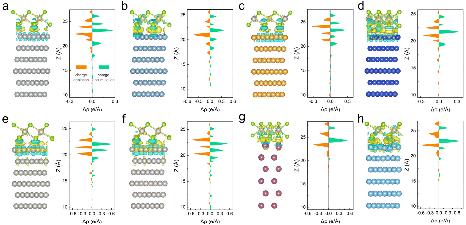 | ||
| Fig. 1 (a)–(h) Side views of the optimized atomic structures and three-dimensional and plane charge density differences for Ag, Al, Au, Cu, Pd, Pt, Sc and Ti-based metal–monolayer PtSe2 contacts. For three-dimensional charge density differences, yellow and cyan regions represent the charge accumulation and depletion, respectively. For convenient viewing and comparison, the isosurface of charge density differences is 0.002e bohr−3 for Ag, Al, Au, and Cu-based contacts; 0.004e bohr−3 for Pd, Pt, Sc, and Ti-based contacts. | ||
To study the interfacial interaction of 2D PtSe2 and metals, we first calculated the binding energy (see Table S3†) according to the following equation: Eb = (Emetal + EPtSe2 − Eheterostructure)/A, where Emetal, EPtSe2, and Eheterostructure are the total energy of the isolated metal, isolated PtSe2 and metal–PtSe2 system, and A is the interfacial area. The binding energy can be classified into three categories. Al and PtSe2 form a relatively weak bonding with an Eb of 0.97 J m−2, Ag and Au form a relatively middle bonding with PtSe2 with an Eb of 1.27 and 1.23 J m−2, respectively, while Cu, Pd, Pt, Sc and Ti form a relatively strong bonding with PtSe2 with the Eb range of 1.82–2.61 J m−2. The corresponding charge transfers based on Bader charge analysis are 0.07, 0.4, −0.02, 0.11, −0.03, −0.08, 0.61 and 0.59e. In addition, we found that the variation trends of the average interlayer distance in metal–PtSe2 contacts (defined as the average distance between the Se atoms and metal atoms at the interface) is also consistent with the change of banding energy, suggesting that the distance can be well applied as an indicator for describing the binding strength between different metals and PtSe2. Significantly, as shown in Table S4,† we found that the binding energy for all metal–PtSe2 systems are obviously higher than those for previously reported metal–MoS2,27,28 metal–MoSe2,29 metal–WS2![[thin space (1/6-em)]](https://www.rsc.org/images/entities/char_2009.gif) 30 and metal–WSe2 systems,31 indicating the significant strong interfacial interactions between PtSe2 and metals.
30 and metal–WSe2 systems,31 indicating the significant strong interfacial interactions between PtSe2 and metals.
The strong interactions between metals and 2D PtSe2 were further investigated by calculating the charge redistribution at the interface, which plays an important role in determining the electronic structures of the metal–PtSe2 system. Charge density difference analysis perpendicular to the interface of metal–PtSe2 was performed according to the equation: Δρ = ρmetal–PtSe2 − ρmetal − ρPtSe2. As shown in Fig. 1, there exists a significant charge accumulation region, which indicates the formation of a strong overlap of electronic orbitals at the interface. In addition, the simultaneous charge depletion region near the Se and metal atoms at the interface also demonstrates a large charge transfer between PtSe2 and metals. Importantly, we found that the maximum values of charge accumulation for Sc, Ti, Pd and Pt are obviously larger than those of charge accumulation for Ag, Al, Au and Cu, which agrees well with the bonding strength for these metal–PtSe2 systems. Besides the charge redistribution at the interface, significant charge accumulation and charge depletion also appear for the inner atom layers of both metals and PtSe2, which again demonstrates strong interactions between PtSe2 and metals.
Band structures and FLP effect
We now study the band structures of metal–PtSe2 contacts to discuss the effect of interfacial interactions on the band alignment of PtSe2 and metals. As shown in Fig. S1,† our calculation results show that the original monolayer PtSe2 is an indirect semiconductor with a band gap of 1.36 eV at the level of PBE functional, which is consistent with the previous studies.18 However, the formation of contacts with all metals leads to the seriously destroyed band structure of PtSe2 and significant metal induced mid-gap states, which is the main reason for the FLP effect (see Fig. 2 and Fig. S3†).32,33 We found that the PtSe2-dominated bands always across the Fermi level for all the metal–PtSe2 systems, demonstrating the hybridization of states of interfacial PtSe2 and metals. In addition, the degree of hybridization is proportionate to the binding strength between metals and PtSe2. These results are different from the case for MoS2, in which the states of MoS2 are weakly destroyed.27,28 Our results again demonstrate that the strong interfacial interactions lead to a strong hybridization and thus effective electron ejections from metals to PtSe2 at the vertical interface.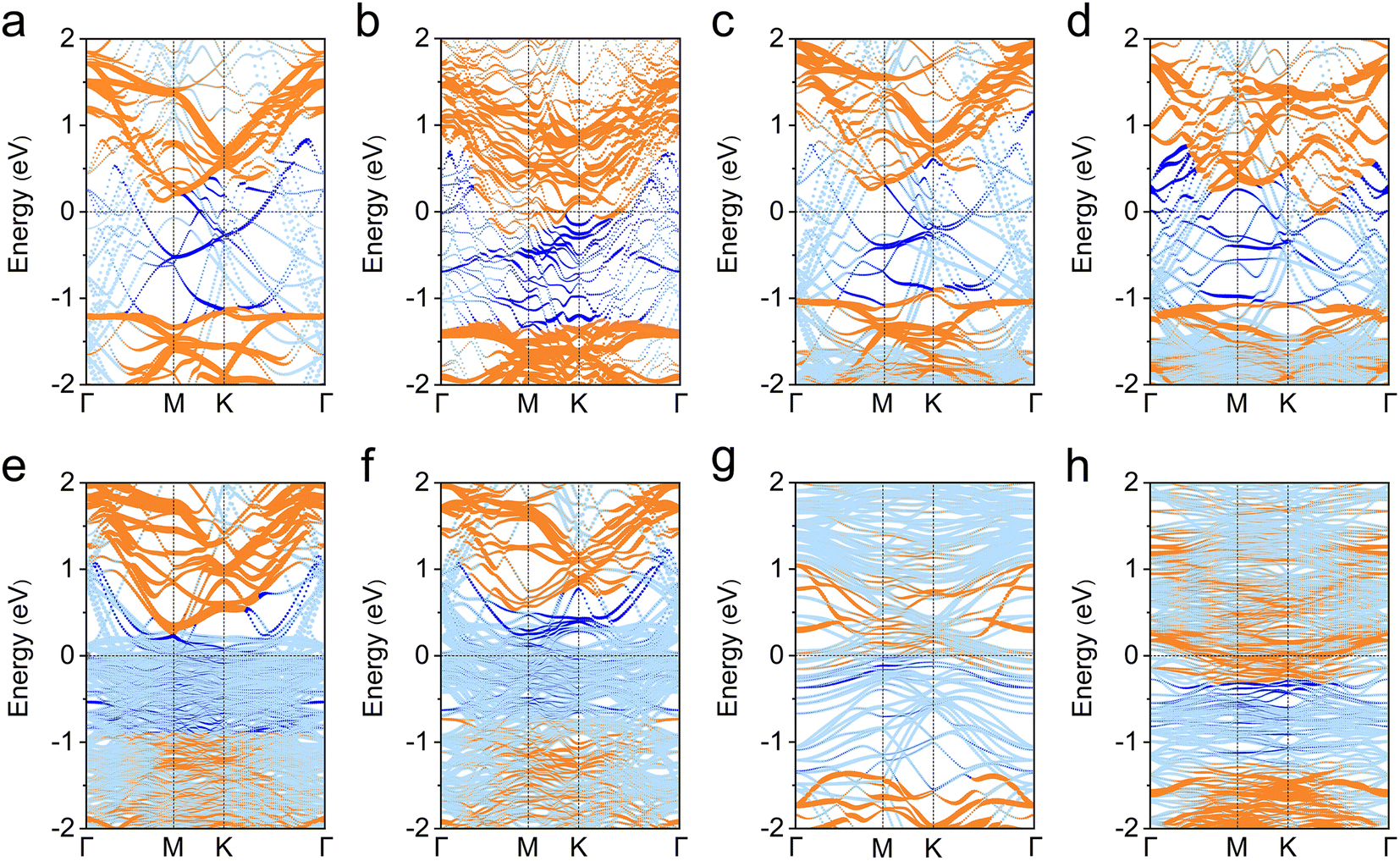 | ||
| Fig. 2 (a)–(h) Projected band structures of Ag, Al, Au, Cu, Pd, Pt, Sc and Ti-based metal–monolayer PtSe2 contacts. Orange and blue colors represent the contributions from PtSe2 and metals, respectively. The main meta-induced mid-gap states are indicated by blue color. The original projected band structures are shown in Fig. S3.† | ||
To further study the underlying hybridization between different orbitals in the metal–PtSe2 system, the partial densities of states (PDOSs) of Pt and Se orbitals for PtSe2 and metals were calculated (see Fig. 3). For the original PtSe2 without contact with metals, the PDOSs of Pt and Se orbitals with the intrinsic band gap are shown in Fig. S1.† The conduction band minimum (CBM) and the valence band maximum (VBM) are mainly contributed by the s and p orbitals of Se atoms and the d orbitals of the Pt atom. After the formation metal–PtSe2 contacts, we found that significant Pt and Se states penetrate deep into the intrinsic band gap of the original PtSe2 and thus forms infiltrated gap states for all the metal–PtSe2 contacts, which is one of the main contributions of the FLP effect. In addition, as can be seen from the band structures of the metal–PtSe2 contacts, the Fermi level of the metal–PtSe2 systems is always near the CBM of the PtSe2 part, which again demonstrates a significant FLP effect at the interface. On one hand, the main contributions of the infiltrated gap states are still from the s and p orbitals of Se atoms and the d orbitals of the Pt atom. On the other hand, we found that the value of PDOS at the Fermi level varies significantly due to the different bonding strengths for different metal–PtSe2 systems, which are significantly larger than the value of the corresponding PDOS value of Mo(W)S(Se)2-based contacts.27–31 Therefore, our results again demonstrate the strong band hybridization at the interface.
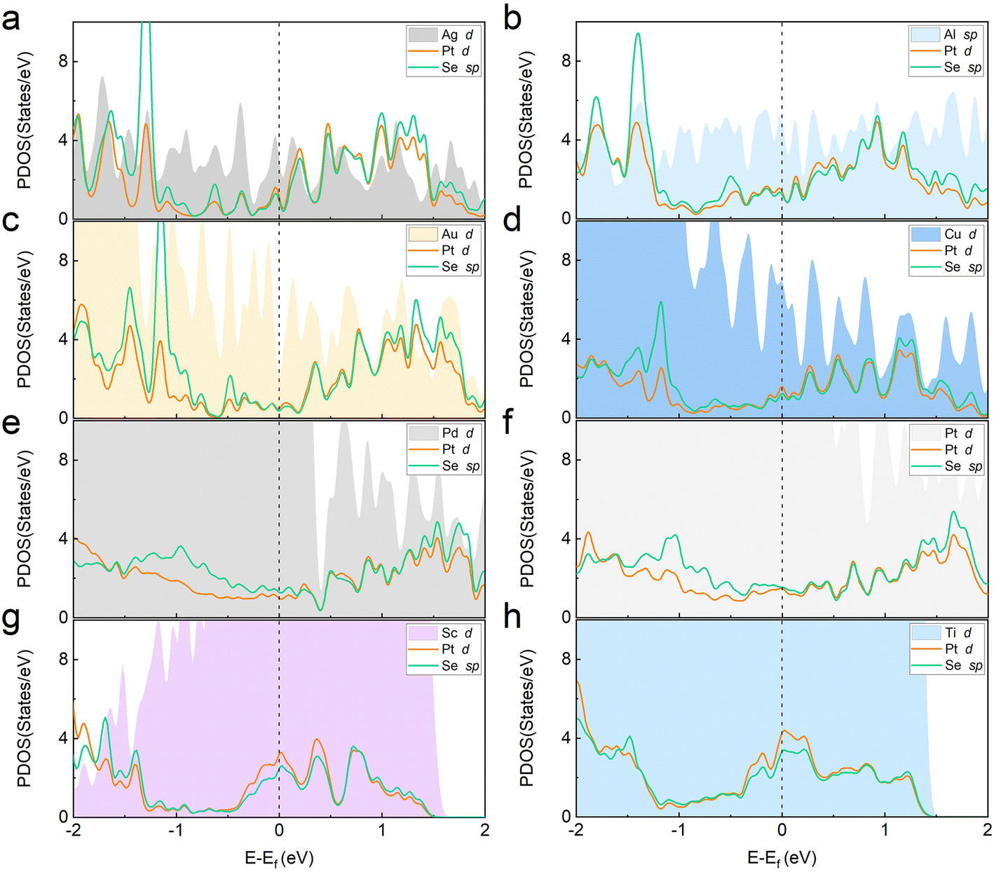 | ||
| Fig. 3 (a)–(h) Partial densities of states for PtSe2 and metals in Ag, Al, Au, Cu, Pd, Pt, Sc and Ti-based metal–monolayer PtSe2 contacts. | ||
As one of important factors that determine the carrier transport efficiency, we now discuss the Schottky barrier at the vertical interface based on the energy difference between the Fermi level of the metal–PtSe2 contacts and the band edge energies of PtSe2 in the metal–PtSe2 contacts.32 As shown in Fig. 2, by referring to the original band structures of supercell PtSe2 in contacts (see Fig. S4†), we found that Ag, Au, Pd, and Pt form n-type Schottky contacts with PtSe2, which is due to the relatively higher work function of these metals. In addition, the Schottky barrier is low within the range of 0.13–0.54 eV. The Ag–PtSe2 contact shows the lowest Schottky barrier of 0.13 eV, indicating the promising application in n-type contact-based electronics. On the other hand, we found that due to the relatively low work function of Al, Cu, Sc and Ti, there appear Ohmic contacts when contacting with PtSe2. The FLP effect was further investigated by fitting the FLP factor S. As shown in Fig. S5,† the p-type Schottky barrier height decreases linearly with increasing the work function of metals, and the FLP factor S is 0.32, which demonstrates the strong FLP effect for the metal–PtSe2 contacts.33
It is noteworthy that the Schottky barrier may exist at the vertical interface or the lateral contact due to the different strengths of interfacial interactions.31 For Al, Cu, Sc and Ti-based contacts, the overall vertical metal–PtSe2 interface can be considered as a metallic system considering the band of PtSe2 crossing the Fermi level. Therefore, it is necessary to study whether the lateral Schottky barrier forms in the lateral contact region that bridges the metal–PtSe2 systems and the free PtSe2 in the channel region (see Fig. S2d†). Here, we preliminarily evaluated the Schottky barrier in the lateral contact region based on the work function approximation method. The Schottky barrier is defined as the energy difference between the Fermi level of the metal–PtSe2 contact system and the CBM or VBM of PtSe2 in the channel region.
As shown in Fig. S7,† we found that Al, Cu, Sc, and Ti form the n-type lateral Schottky contacts with PtSe2, which is partly due to the relatively low work function of these metals. In addition, the Schottky barrier is relatively low within the range of 0.34–0.55 eV, indicating the promising application of these metals in n-type semiconductor-based electronics. To further confirm the validity of our results, we have modelled the large enough supercell that includes the vertical metal–PtSe2 interface and the free PtSe2 in the channel region. As shown in Fig. 4, we took the Al–PtSe2 system as an example, in the vertical interface region, Al forms an Ohmic contact with PtSe2 with a significant mid-gap state, which is consistent with the results discussed above. However, the overall vertical metallic Al–PtSe2 system forms a lateral n-type contact with PtSe2 in the channel region. Similar results can also be found for Cu, Sc and Ti-based systems (see Fig. S6†). More importantly, as shown in Fig. S7,† we found that the variation trends of the SBH-based supercell model are similar to that based on the work function approximation, with a difference of only 0.1–0.2 eV, which effectively demonstrates the validity of our results.
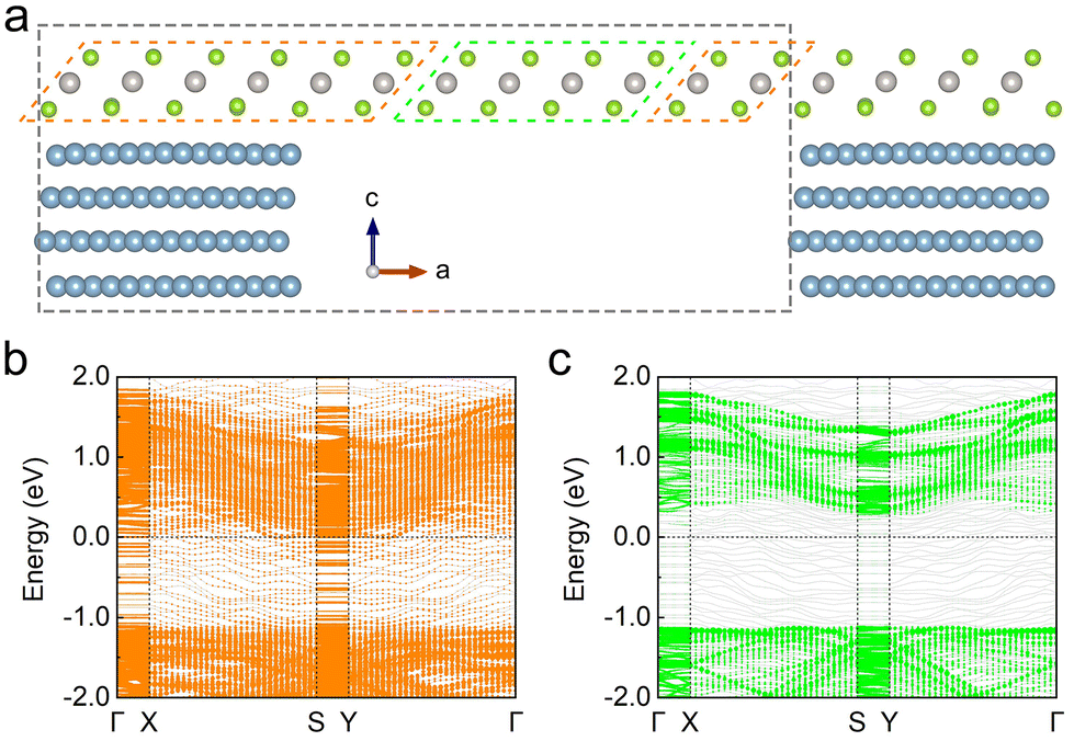 | ||
| Fig. 4 (a) Large supercell (indicated by the grey dashed line with a vacuum of 15 Å) that includes the vertical metal contact region (indicated by the orange dashed line) and the lateral free-standing PtSe2 region (indicated by the green dashed line). (b) and (c) represent the band structures of PtSe2 in the vertical metal contact region and the lateral region, respectively (note that the Fermi level is the same for (b) and (c)). | ||
Interfacial tunneling barrier and tunneling-specific resistivity
Considering that the strong interfacial interaction is positively convenient for electron injection from metal electrodes to 2D materials. We now further study the detailed tunneling behaviors at the interface that plays an important role in determining the efficiency of charge injection in electronics. The average electrostatic potential perpendicular to interface of metal–PtSe2 contacts is shown in Fig. 5. As two important parameters for evaluating the tunneling barrier, the barrier height is defined as the energy difference between the Fermi level of the metal–PtSe2 system and the maximum of the potential energy at the metal–PtSe2 interface, while the tunneling barrier width is defined as the corresponding full width at half maximum of the tunneling barrier height. Therefore, the tunneling barrier height and width represent the lowest barrier for charge injection from metals to PtSe2.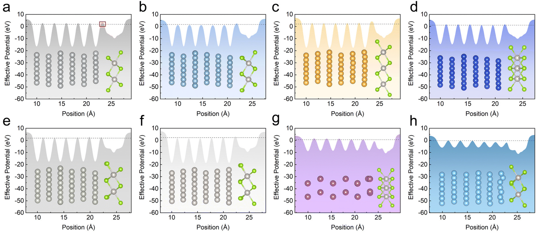 | ||
| Fig. 5 (a)–(h) Effective potential along the vertical direction for Ag, Al, Au, Cu, Pd, Pt, Sc and Ti-based metal–monolayer PtSe2 contacts. The dotted line represents the Fermi energy level. | ||
By comparing the covalent distance (sum of the covalent radii of the metal atom and the Se atom) with the actual distance between the metal atom and the interfacial Se atom in contacts, we found that only part of the actual distances are shorter than the covalent distance, indicating the formation of relatively weak chemical bonds (see Table S5†). In addition, compared with the cases of the van der Waals interlayer distance (3.5 Å) between metal and PtSe2 (see Table S6†), these weak chemical bonds only overcome the tunneling barrier for Sc and Ti-based contacts. However, the tunneling barrier that electrons need to overcome for tunneling still exists in Ag, Al, Au, Cu, Pd and Pt-based contacts. Therefore, it is essential to study tunneling probability in metal–PtSe2 contacts.
The tunneling probability (TB) can be qualitatively evaluated using the following eqn (1):34–36
 | (1) |
Besides the tunneling probability, the tunneling-specific resistivity is another key parameter for evaluating the quality of metal–semiconductor contacts. Here, considering the relatively low tunneling barrier and tunneling width, we have estimated the tunneling-specific resistivity (ρt) based on the Simmons tunneling injection model under the low-bias approximation that is expressed in the following eqn (2):3,36
 | (2) |
Differences in metal–bilayer PtSe2 and metal–monolayer PtSe2 contacts
It is known that there exists strong interlayer interaction that leads to significant changes in the electronic structure of multilayer PtSe2.18,20 It is necessary to study the effect of strong interlayer interaction in bilayer PtSe2 on the interfacial interactions between metals and bilayer PtSe2. Compared with the metal–monolayer PtSe2 contacts, the binding energy for metal–bilayer PtSe2 contacts increases slightly, which is due to the stronger interaction indicated by the lager charge transfer (see Table S3 and Fig. S8†). The electronic structures of metal–bilayer PtSe2 were further studied. As shown in Fig. S9,† it is expected that there appears a large amount of infiltrated gap states in the band gap of PtSe2. In addition, the density of states at the Fermi level for bilayer PtSe2 are obviously larger than that of monolayer PtSe2 (see Fig. S10†), which is caused by the stronger interfacial interactions in metal–bilayer PtSe2. By referring to the original band structures of supercell PtSe2 in contacts (see Fig. S4†), we found that the FLP factor is 0.26 (see Fig. S11†), which is due to the enhanced interfacial interactions for metal–BL PtSe2. Therefore, our results indicate that it is difficult to tune the FLP effect based on the layer numbers of 2D materials.The effect of layer number on the tunneling behavior was also further investigated. As shown in Fig. S12 and Table S8,† besides the tunneling barrier at the metal (including Ag, Al, Au, Cu, Pd and Pt) and the first-layer PtSe2, there also exists a tunneling barrier between the first-layer PtSe2 and the second-layer PtSe2, while there only exists the tunneling barrier between the first-layer PtSe2 and the second-layer PtSe2 for Sc and Ti. In addition, we found that the tunneling probability increases slightly compared with the metal and monolayer PtSe2 contacts. Therefore, these results again indicate the stronger interfacial interactions for metal–bilayer PtSe2 than that for metal–monolayer PtSe2. Interestingly, compared with the tunneling behaviors at the interface for free bilayer PtSe2 (see Fig. S13†), we found that the tunneling behaviors at the interface between the first-layer PtSe2 and the second-layer PtSe2 are also slightly influenced by different metals with tunneling probabilities of 39.6%–46.2%. More importantly, we found that for Ag and Au, the tunneling probability at the interface for metal-first layer PtSe2 is similar to that at the interface for the first- and second-layer PtSe2. However, for Al, Cu, Pd and Pt, the tunneling probability at the interface for metal–first layer PtSe2 is significantly higher than that at the interface for the first- and second-layer PtSe2, which indicates that the charge injection from first layer to second layer is hindered. For Sc and Ti, the tunneling behavior from first-layer to second-layer PtSe2 is also limited by the tunneling barrier with a probability of 43.7% and 46.2%, respectively.
Mechanism of interfacial interactions and interfacial dipole for metal–PtSe2 contacts
We now turn to discuss the underlying mechanism of the interfacial behaviors in metal–PtSe2 contacts. Since the interfacial behaviors is directly determined by the strength of interfacial interactions, we first discuss the dependency relationship between the FLP effect/tunneling behaviors and the interfacial binding energy. As shown in Fig. 6a, the FLP factors of several 3D and vdW-type metal–semiconductors are listed for comparison.32 We found that the overall FLP factors decrease with increasing interfacial binding energy, indicating the increasing strength of FLP effect. In addition, the FLP factor of metal–BL PtSe2 is smaller than that of metal–ML PtSe2 due to the larger binding energy in metal–BL PtSe2, which is consistent with the overall relationship between the FLP factor and the binding energy. As shown in Fig. 6b, we found that the carrier tunneling probability of both metal–ML PtSe2 and metal–BL PtSe2 also increases with increasing interfacial binding energy, which is due to that the stronger interfacial interactions lead to the decreased tunneling barrier height and width.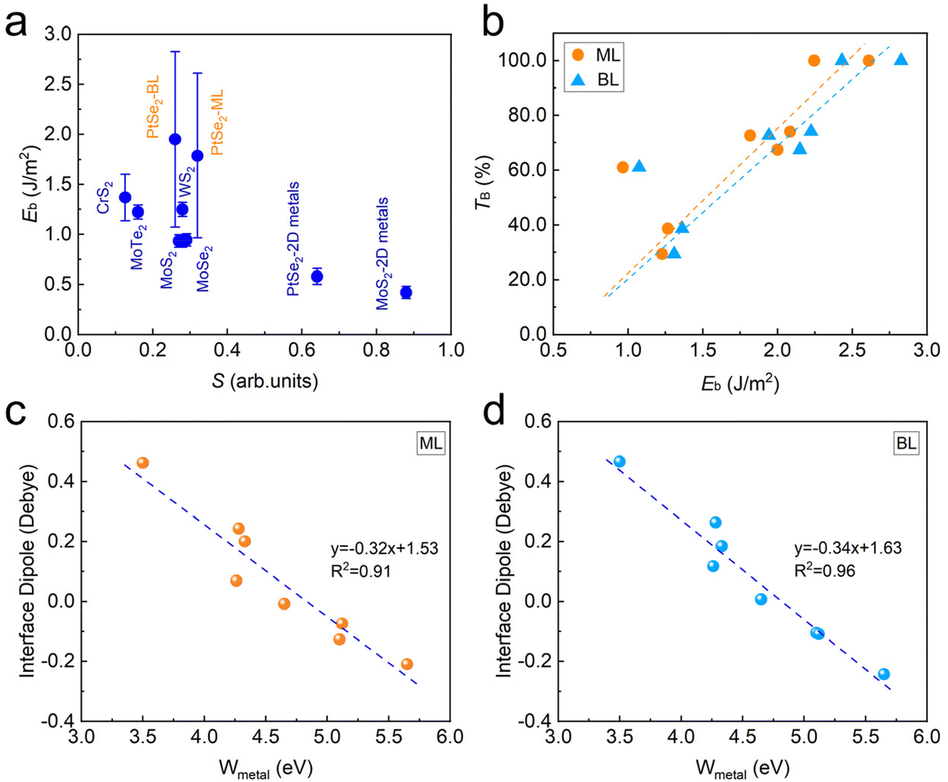 | ||
| Fig. 6 (a) Interfacial binding energy versus the FLP factor S in metal–PtSe2 contacts and other semiconductor-based contacts,32 (b) tunneling probability in metal–PtSe2 contacts versus the interfacial binding energy, (c) interface dipole of metal–monolayer PtSe2 and (d) metal-bilayer PtSe2versus the work function of metals. | ||
As discussed above, for all metal–PtSe2 contacts, the interfacial metal atoms and Se atoms form chemical bonds with binding energies of 0.97–2.61 J m−2. Therefore, we now discuss the bond length of the interfacial Se atom and Pt atom in PtSe2 to investigate the effect of interfacial chemical bonds on the inner disorder of PtSe2. As shown in Fig. S14,† compared with the original bond length of Se–Pt in isolated PtSe2, the average bond length of the interfacial Se atom and Pt atom increases for almost all metal–PtSe2 (monolayer and bilayer) contacts. For Al and Au, the bond length is almost unchanged, which is likely due to the absence of d orbitals for Al and full filled d-orbitals for Au, respectively. Therefore, the interfacial chemical bonds weaken the inner interactions between interfacial Se atoms and Pt atoms in PtSe2. These inner disorders of PtSe2 in turn disturb the electronic structures of PtSe2, leading to the formation of infiltrated gap states, and finally contribute to the FLP effect.
As discussed above, the formation of metal–PtSe2 contacts leads to a large amount of asymmetric charge redistribution between metals and PtSe2. Therefore, it is necessary to investigate whether the dipole exists in the interface region. Here, we define the average interfacial dipole Da = Dcontact/N, where Dcontact is the total interfacial dipole and N is the number of Se atoms at the interface. As shown in Fig. 6c and d, there indeed appears a significant interfacial dipole due to the charge redistribution in the interface region for both metal–monolayer PtSe2 and metal–bilayer PtSe2. More importantly, we found that the interfacial dipole exhibits an obviously linear dependence on the work function of metals. This is because the strength of the interfacial dipole is largely related to the degree of charge rearrangement at the interface, which is largely dependent on the work function of metals.27 In addition, we found that the slope of the relationship between the dipole and the work function of a pure metal for monolayer PtSe2 is similar to that for bilayer PtSe2, which is due to the fact that charge redistribution mainly occurs between the first layer PtSe2 and metals. Moreover, we found that for both metal–monolayer and metal–bilayer contacts, the dependency of interfacial dipole on the work function is similar to the dependency of Schottky barrier on the work function, which indicates that the Fermi level of the metal–PtSe2 contacts is strongly related to the interfacial dipole induced by charge redistribution. Therefore, the size of interfacial dipole is suggested to be a key factor for regulating the Schottky barrier height for metal and semiconductor systems, which can be further explored by means of alloys, interface doping, interface passivation and so on.
Schemes for suppressing strong FLP effect
Although the metal–PtSe2 contacts exhibit a low Schottky barrier and show promising applications in electronics, the strong FLP effect is still not conducive to practical manipulations. Therefore, it is crucial to suppress the strong FLP effect for further applications. We now introduce h-BN as an interfacial buffer layer to try to suppress the strong FLP effect in metal–PtSe2 contacts. As shown in Fig. 7a, Ag, Al, Au, Pd, Pt and Ti-based metal–BN–PtSe2 contacts were studied here considering the feasible lattice match. The most stable stacking configurations were obtained by considering different possible stacking modes. The corresponding lattice constant and interfacial distance are listed in Table S9.†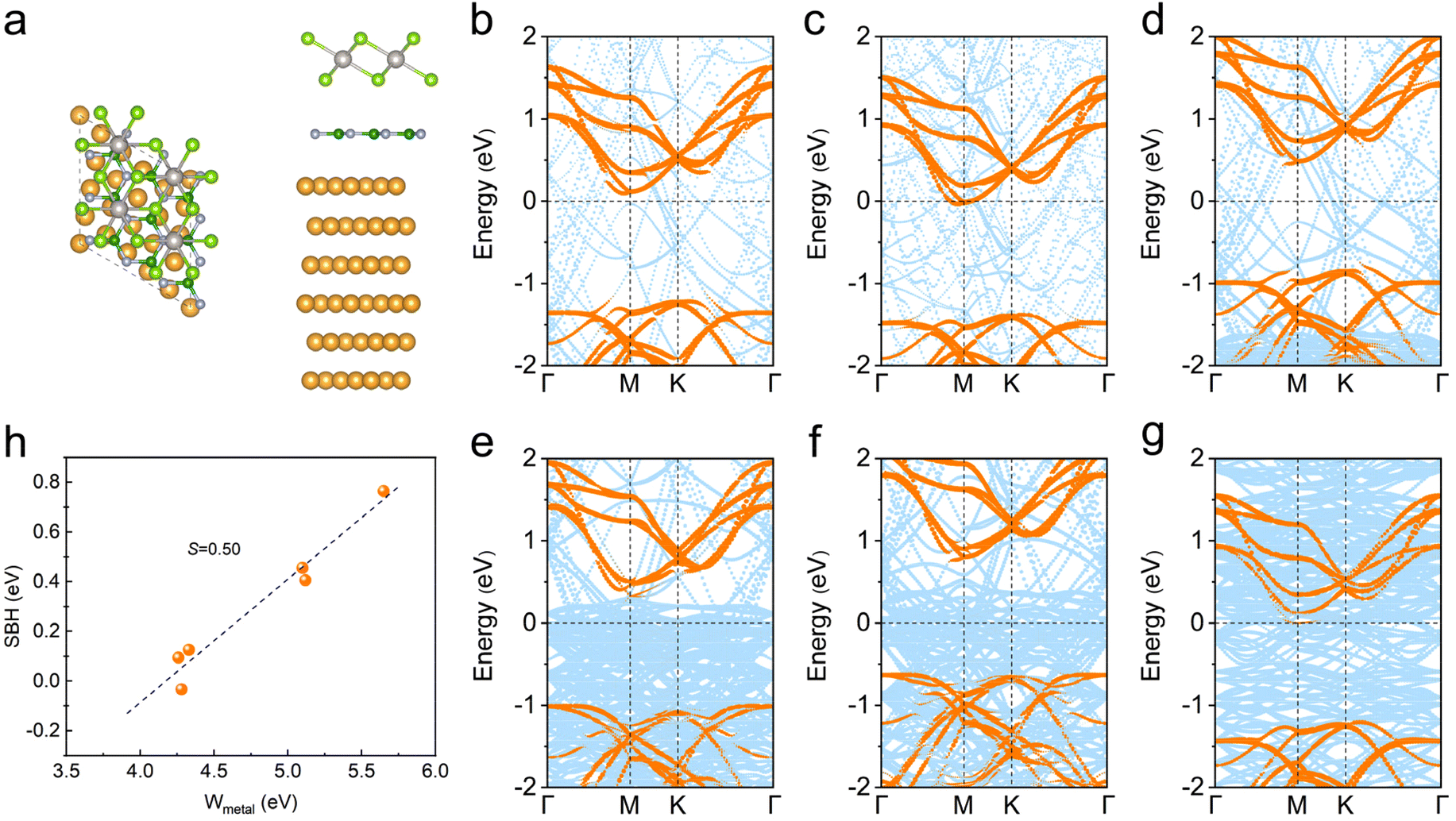 | ||
| Fig. 7 (a) Atomic structures of metal–BN–monolayer PtSe2 and (b) projected band structures of Ag, Al, Au, Pd, Pt and Ti-based metal-BN-monolayer PtSe2 contacts, and the FLP factor of metal–BN–monolayer PtSe2. | ||
As shown in Fig. 7b–g, we found that PtSe2 still forms an Ohmic contact with the Al metal. In addition, PtSe2 forms n-type Schottky contacts with Ag and Ti with low barriers (0.09 and 0.13 eV) due to the low work function. The number of n-type Schottky barriers increases with increasing work function for Au and Pd. Further increasing the work function for Pd, it is noteworthy that PtSe2 forms a p-type Schottky contact with the Pt metal, which is different from the case of the original Pt–PtSe2. In Fig. 7h, the FLP factor S is fitted as 0.50, demonstrating the reduced FLP effect in metal–BN–PtSe2 contacts. Therefore, the introduction of a buffer layer to metal–semiconductor systems is proved as an effective scheme to suppress the strong FL effect. Besides, other promising schemes such as the introduction of vdW 2D semimetals32 and the atomic passivation on the metal surface37 are also considered as effective ways to suppress the strong FL effect, which will be discussed in our future studies.
Conclusions
In summary, we have systematically investigated the interfacial properties of contacts between PtSe2 and a series of potential metal electrodes based on density functional theory (DFT) calculations. We found that the interfacial Se atom of PtSe2 forms weak chemical bonds with metal atoms with significant charge rearrangement at the interface. In addition, the strong interfacial interactions lead to vertical Schottky contacts for PtSe2 with Ag, Au, Pd and Pt, while lateral Schottky contacts for PtSe2 with Al, Cu, Sc and Ti. Moreover, we found that all metal–PtSe2 contacts exhibit high tunneling probability and low tunneling-specific resistivity that are two orders of magnitude lower than those of the state-of-the-art contacts, demonstrating high-efficiency electron injection. By introducing h-BN as a buffer layer, we found that the Pt–PtSe2 contacts transform into p-type Schottky contacts and the FLP effect is weakened with S = 0.50. Therefore, our results provide insight into the interface properties of metal–PtSe2 contacts, which is useful for the practical application of PtSe2 in high-performance electronics.Computational methods
All calculations were performed using the Vienna ab initio simulation package (VASP) with the Perdew–Burke–Ernzerhof (PBE) exchange–correlation functional and the projector-augmented wave (PAW) method.38–40 For geometry optimization, van der Waals interactions are considered by using the DFT-D3 method of Grimme.41 A plane-wave energy cutoff of 500 eV and fine k-sampling with a separation of 0.025 Å−1 in the Brillouin zone were set for all calculations. The convergence criteria for total energy and maximal residual force were set 1.0 × 10⁻⁶ eV and 0.01 eV Å−1, respectively. A vacuum layer of 20 Å perpendicular to the metal–PtSe2 contact was set to prevent the interaction between the neighboring slabs. During the optimization of atom position, the PtSe2 layer and the adjacent two layer metals are fully relaxed while the outward four layer metals are fixed.Due to the large supercell of metal–PtSe2 contacts (54 atoms for Ag, Al, Au, Pd, Pt and Ti; 51 atoms for Cu; 33 atoms for Sc), the small system of Sc–PtSe2 contact is taken as an example for HSE06-based band structural calculations to check the validity of our results. As shown in Fig. S15,† we found that the relative energy position of the conduction band and Fermi level energy calculated by the HSE06 functional is similar to that calculated by the PBE functional, with an energy shift of only 0.09 eV. In addition, the Sc–PtSe2 contact still keeps the Ohmic-type contact for HSE06-based results. Therefore, the PBE functional is applied here to study the band structure of metal–PtSe2 contacts.
The metal–PtSe2 contacts are built with PtSe2 and six-layer metals. To minimize the lattice mismatch of metal–PtSe2 heterostructures, we combined the  supercell of an Ag/Al/Au/Pd/Pt (111) surface with the 2 × 2 × 1 supercell of PtSe2, the
  supercell of a Cu (111) surface with the
  supercell of PtSe2, the 2 × 2 × 1 supercell of a Sc (001) surface with the
  supercell of PtSe2, and the
  supercell of a Ti (001) surface with the 2 × 2 × 1 supercell of PtSe2. The lattice constants of the supercell metal–PtSe2 contacts are adopted as the average of the lattice parameters of the supercell metal and supercell PtSe2. The corresponding lattice mismatches are all less than 3.6% and the corresponding strains introduced to PtSe2 are all less than 2% (see Table S10†). For the largest compression strain in Cu–PtSe2 (1.79%) and the largest tension strain in Pd–PtSe2 (−1.75%), the band gap of PtSe2 only changes by 0.14 eV and 0.01 eV, which indicates the validity of our results.
Conflicts of interest
The authors declare no conflict of interest.Acknowledgements
We acknowledge the financial support from the National Natural Science Foundation of China (62022081, 61974099, 62204240), the Science Fund for Creative Research Groups of the National Natural Science Foundation of China (62121005), the National Key Research and Development Program (2021YFA0717600), the Natural Science Foundation of Jilin Province (20210101173JC and 20220508030RC), and the Changchun Key Research and Development Program (21ZY03).References
- Y. Liu, J. Guo, E. Zhu, L. Liao, S. J. Lee, M. Ding, I. Shakir, V. Gambin, Y. Huang and X. Duan, Nature, 2018, 557, 696 CrossRef CAS PubMed.
- D. Akinwande, C. Huyghebaert, C.-H. Wang, M. I. Serna, S. Goossens, L.-J. Li, H. S. P. Wong and F. H. L. Koppens, Nature, 2019, 573, 507 CrossRef CAS PubMed.
- P. C. Shen, C. Su, Y. Lin, A. S. Chou, C. C. Cheng, J. H. Park, M. H. Chiu, A. Y. Lu, H. L. Tang, M. M. Tavakoli, G. Pitner, X. Ji, Z. Cai, N. Mao, J. Wang, V. Tung, J. Li, J. Bokor, A. Zettl, C. I. Wu, T. Palacios, L. J. Li and J. Kong, Nature, 2021, 593, 211 CrossRef CAS PubMed.
- Y. Wang, J. C. Kim, Y. Li, K. Y. Ma, S. Hong, M. Kim, H. S. Shin, H. Y. Jeong and M. Chhowalla, Nature, 2022, 610, 61 CrossRef PubMed.
- P. Luo, C. Liu, J. Lin, X. Duan, W. Zhang, C. Ma, Y. Lv, X. Zou, Y. Liu, F. Schwierz, W. Qin, L. Liao, J. He and X. Liu, Nat. Electron., 2022, 5, 849 CrossRef CAS.
- Y. Liu, X. Duan, H.-J. Shin, S. Park, Y. Huang and X. Duan, Nature, 2021, 591, 43 CrossRef CAS PubMed.
- S. Das, A. Sebastian, E. Pop, C. J. McClellan, A. D. Franklin, T. Grasser, T. Knobloch, Y. Illarionov, A. V. Penumatcha, J. Appenzeller, Z. Chen, W. Zhu, I. Asselberghs, L.-J. Li, U. E. Avci, N. Bhat, T. D. Anthopoulos and R. Singh, Nat. Electron., 2021, 4, 786 CrossRef CAS.
- J. Bullock, M. Amani, J. Cho, Y.-Z. Chen, G. H. Ahn, V. Adinolfi, V. R. Shrestha, Y. Gao, K. B. Crozier, Y.-L. Chueh and A. Javey, Nat. Photonics, 2018, 12, 601 CrossRef CAS.
- G. Gui, J. Li and J. Zhong, Phys. Rev. B: Condens. Matter Mater. Phys., 2008, 78, 075435 CrossRef.
- A. Favron, E. Gaufrès, F. Fossard, A.-L. Phaneuf-L'Heureux, N. Y. W. Tang, P. L. Lévesque, A. Loiseau, R. Leonelli, S. Francoeur and R. Martel, Nat. Mater., 2015, 14, 826 CrossRef CAS PubMed.
- A. Rawat, N. Jena and A. De Sarkar, J. Mater. Chem. A, 2018, 6, 8693 RSC.
- X. Yu, P. Yu, D. Wu, B. Singh, Q. Zeng, H. Lin, W. Zhou, J. Lin, K. Suenaga, Z. Liu and Q. J. Wang, Nat. Commun., 2018, 9, 1545 CrossRef PubMed.
- A. Avsar, A. Ciarrocchi, M. Pizzochero, D. Unuchek, O. V. Yazyev and A. Kis, Nat. Nanotechnol., 2019, 14, 674 CrossRef CAS PubMed.
- G. Wang, Z. Wang, N. McEvoy, P. Fan and W. J. Blau, Adv. Mater., 2021, 33, 2004070 CrossRef CAS PubMed.
- H. Xu, H. Zhang, Y. Liu, S. Zhang, Y. Sun, Z. Guo, Y. Sheng, X. Wang, C. Luo, X. Wu, J. Wang, W. Hu, Z. Xu, Q. Sun, P. Zhou, J. Shi, Z. Sun, D. W. Zhang and W. Bao, Adv. Funct. Mater., 2018, 29, 1805614 CrossRef.
- N. Sefidmooye Azar, J. Bullock, V. R. Shrestha, S. Balendhran, W. Yan, H. Kim, A. Javey and K. B. Crozier, ACS Nano, 2021, 15, 6573 CrossRef CAS PubMed.
- H. Ma, Q. Qian, B. Qin, Z. Wan, R. Wu, B. Zhao, H. Zhang, Z. Zhang, J. Li, Z. Zhang, B. Li, L. Wang and X. Duan, Adv. Sci., 2022, 9, 2103507 CrossRef CAS PubMed.
- R. A. B. Villaos, C. P. Crisostomo, Z.-Q. Huang, S.-M. Huang, A. A. B. Padama, M. A. Albao, H. Lin and F.-C. Chuang, npj 2D Mater. Appl., 2019, 3, 2 CrossRef.
- D. Wu, Y. Wang, L. Zeng, C. Jia, E. Wu, T. Xu, Z. Shi, Y. Tian, X. Li and Y. H. Tsang, ACS Photonics, 2018, 5, 3820 CrossRef CAS.
- Y. Zhao, J. Qiao, Z. Yu, P. Yu, K. Xu, S. P. Lau, W. Zhou, Z. Liu, X. Wang, W. Ji and Y. Chai, Adv. Mater., 2017, 29, 1604230 CrossRef PubMed.
- S. Song, Y. Sim, S.-Y. Kim, J. H. Kim, I. Oh, W. Na, D. H. Lee, J. Wang, S. Yan, Y. Liu, J. Kwak, J.-H. Chen, H. Cheong, J.-W. Yoo, Z. Lee and S.-Y. Kwon, Nat. Electron., 2020, 3, 207 CrossRef CAS.
- G. Kwon, Y.-H. Choi, H. Lee, H.-S. Kim, J. Jeong, K. Jeong, M. Baik, H. Kwon, J. Ahn, E. Lee and M.-H. Cho, Nat. Electron., 2022, 5, 241 CrossRef CAS.
- Q. Wang, Y. Shao, P. Gong and X. Shi, J. Mater. Chem. C, 2020, 8, 3113 RSC.
- N. Zhao and U. Schwingenschlögl, npj 2D Mater. Appl., 2021, 5, 72 CrossRef CAS.
- G. Su, S. Yang, S. Li, C. J. Butch, S. N. Filimonov, J. C. Ren and W. Liu, J. Am. Chem. Soc., 2019, 141, 1628 CrossRef CAS PubMed.
- J. Du, P. Song, L. Fang, T. Wang, Z. Wei, J. Li and C. Xia, Appl. Surf. Sci., 2018, 435, 476 CrossRef CAS.
- C. Gong, L. Colombo, R. M. Wallace and K. Cho, Nano Lett., 2014, 14, 1714 CrossRef CAS PubMed.
- H. Zhong, R. Quhe, Y. Wang, Z. Ni, M. Ye, Z. Song, Y. Pan, J. Yang, L. Yang, M. Lei, J. Shi and J. Lu, Sci. Rep., 2016, 6, 21786 CrossRef CAS PubMed.
- Y. Pan, S. Li, M. Ye, R. Quhe, Z. Song, Y. Wang, J. Zheng, F. Pan, W. Guo, J. Yang and J. Lu, J. Phys. Chem. C, 2016, 120, 13063 CrossRef CAS.
- H. Tang, B. Shi, Y. Pan, J. Li, X. Zhang, J. Yan, S. Liu, J. Yang, L. Xu, J. Yang, M. Wu and J. Lu, Adv. Theory Simul., 2019, 2, 1900001 CrossRef.
- Y. Wang, R. X. Yang, R. Quhe, H. Zhong, L. Cong, M. Ye, Z. Ni, Z. Song, J. Yang, J. Shi, J. Li and J. Lu, Nanoscale, 2016, 8, 1179 RSC.
- Y. Li, L. Su, Y. Lu, Q. Luo, P. Liang, H. Shu and X. Chen, InfoMat, 2023, e12407 CrossRef CAS.
- C. Kim, I. Moon, D. Lee, M. S. Choi, F. Ahmed, S. Nam, Y. Cho, H. J. Shin, S. Park and W. J. Yoo, ACS Nano, 2017, 11, 1588 CrossRef CAS PubMed.
- X. Zhang, L. Feng, S. Zhong, Y. Ye, H. Pan, P. Liu, X. Zheng, H. Li, M. Qu and X. Wang, Sci. China Mater., 2023, 66, 811 CrossRef CAS.
- Z. Xu, M. Chen and S. F. Liu, J. Phys. Chem. Lett., 2021, 12, 1718 CrossRef CAS PubMed.
- Q. Wang, L. Cao, S.-J. Liang, W. Wu, G. Wang, C. H. Lee, W. L. Ong, H. Y. Yang, L. K. Ang, S. A. Yang and Y. S. Ang, npj 2D Mater. Appl., 2021, 5, 71 CrossRef CAS.
- K.-A. Min, J. Park, R. M. Wallace, K. Cho and S. Hong, 2D Mater., 2016, 4, 015019 CrossRef.
- G. Kresse and D. Joubert, Phys. Rev. B: Condens. Matter Mater. Phys., 1999, 59, 1758 CrossRef CAS.
- J. P. Perdew, K. Burke and M. Ernzerhof, Phys. Rev. Lett., 1996, 77, 3865 CrossRef CAS PubMed.
- P. E. Blöchl, Phys. Rev. B: Condens. Matter Mater. Phys., 1994, 50, 17953 CrossRef PubMed.
- S. Grimme, J. Antony, S. Ehrlich and H. Krieg, J. Chem. Phys., 2010, 132, 154104 CrossRef PubMed.
Footnote |
| † Electronic supplementary information (ESI) available. See DOI: https://doi.org/10.1039/d3nr02466k |
| This journal is © The Royal Society of Chemistry 2023 |