
Quantum-sized topological insulators/semimetals enable ultrahigh and broadband saturable absorption†
Zhexue
Chen
ab,
Xinyu
Sui
bc,
Zhangqiang
Li
ab,
Yueqi
Li
ab,
Xinfeng
Liu
 bc and
Yong
Zhang
*ab
bc and
Yong
Zhang
*ab
aCAS Key Laboratory of Nanosystem and Hierarchical Fabrication, CAS Center for Excellence in Nanoscience, National Center for Nanoscience and Technology, Beijing 100190, P. R. China. E-mail: zhangyong@nanoctr.cn
bUniversity of Chinese Academy of Sciences, Beijing 100049, P. R. China
cCAS Key Laboratory of Standardization and Measurement for Nanotechnology, CAS Center for Excellence in Nanoscience, National Center for Nanoscience and Technology, Beijing 100190, P. R. China
First published on 1st September 2023
Abstract
Two-dimensional topological insulators/semimetals have recently attracted much attention. However, quantum-sized topological insulators/semimetals with intrinsic characteristics have never been reported before. Herein, we report the high-yield production of topological insulator (i.e., Bi2Se3 and Sb2Te3) and semimetal (i.e., TiS2) quantum sheets (QSs) with monolayer structures and sub-4 nm lateral sizes. Both linear and nonlinear optical performances of the QSs are investigated. The QS dispersions present remarkable photoluminescence with excitation wavelength-, concentration-, and solvent-dependence. The solution-processed QSs-poly(methyl methacrylate) (PMMA) hybrid thin films demonstrate exceptional nonlinear saturation absorption (NSA). Particularly, Bi2Se3 QSs-PMMA enables record-high NSA performance with a broadband feature. Specifically, the (absolute) modulation depths up to 71.6 and 72.4% and saturation intensities down to 1.52 and 0.49 MW cm−2 are achieved at 532 and 800 nm, respectively. Such a phenomenal NSA performance would greatly facilitate their applications in mode-locked lasers and related fields.
New conceptsTopological insulators and semimetals are important classes of 2D materials. Their quantum sheets (QSs) can be treated as extremely quantum-sized topological insulators/semimetals, whose production is highly desired but is far from satisfactory. We herein report the high-yield (>12 wt%) production of topological insulator (i.e., Bi2Se3 and Sb2Te3) and semimetal (i.e., TiS2) QSs with monolayer structures and sub-4 nm lateral sizes. The QSs-poly(methyl methacrylate) (PMMA) hybrid thin films demonstrate exceptional nonlinear saturation absorption (NSA). Ultrahigh nonlinear response (72.4 and 68.4%) and ultralow power excitation (0.49 and 0.80 MW cm−2) are simultaneously achieved in both Bi2Se3 QSs-PMMA and TiS2 QSs-PMMA. Such phenomenal NSA performances in quantum-sized topological insulators/semimetals would greatly facilitate their applications in mode-locked lasers and related fields. |
1. Introduction
Two-dimensional (2D) materials have attracted much interest over the past decade due to their fascinating structures and properties.1,2 Topological insulators (e.g., Bi2Se3, Bi2Te3, and Sb2Te3) and semimetals (e.g., TiS2 and TiSe2) are important classes of 2D materials, which have emerged as the new frontiers of materials science.3,4 Both topological insulators and semimetals possess extraordinary properties. The former features a gapless metallic state on their surfaces/edges and insulator characteristics in the bulk,5 while the latter is characterized by bulk Dirac or Weyl fermions and nontrivial topological surface/edge states.6 Such unique materials have been widely applied in various fields such as quantum physics,7 spintronics and magnetoelectronics.3,6 Compared with bulk layered materials and conventional 2D materials, extremely quantum-sized 2D materials (e.g., 2D quantum sheets (QSs)) demonstrate remarkable performances because of their (both in-plane and out-of-plane) quantum confinement and prominent edge effects.8 The production of 2D QSs of topological insulators and semimetals is highly desired but far from satisfactory. Fortunately, we have recently developed a general strategy towards the production of 2D QSs and zero-dimensional quantum dots (0D QDs) from their bulk materials.8–13 However, whether the strategy could be applied for topological insulator and semimetal QS production has never been testified.Nonlinear optical (NLO) response is the key factor for the evaluation of NLO materials. As a typical third-order NLO effect, nonlinear saturation absorption (NSA) has attracted growing attention due to their applications in mode-locked lasers and related fields.14 2D materials have shown their great potential in NSA by having a deep modulation depth and low saturation intensity.15 Recently, quantum-sized materials have demonstrated exciting NSA performances.8–13 Meanwhile, topological insulators and semimetals are interesting candidates for NSA thanks to their unique electronic structures.16,17 Therefore, quantum-sized topological insulators and semimetals could be very promising in terms of NSA performances.
Herein, we report the successful production of topological insulator (i.e., Bi2Se3 and Sb2Te3) and semimetal (i.e., TiS2) QSs directly from their bulk materials using an all-physical top-down method. The combination of silica-assisted ball-milling and sonication-assisted solvent exfoliation enabled the high-yield (>12 wt%) production of QSs with monolayer structures and extremely reduced lateral sizes (<4 nm). The as-produced QSs were structurally intrinsic, which could be determinative to their unique photoluminescence (PL) and NSA performances. The QS dispersions presented excitation wavelength-, concentration-, and solvent-dependent PL. The QSs-poly(methyl methacrylate) (PMMA) hybrid thin films demonstrated exceptional NSA performances. Particularly, the Bi2Se3 QSs-PMMA realized ultrahigh nonlinear response and ultralow power excitation at wavelengths of 532 and 800 nm.
2. Results and discussion
The production process of Bi2Se3 QSs is schematically illustrated in Fig. 1(a), where four sequential procedures: silica-assisted ball-milling, sonication-assisted solvent exfoliation, centrifugation and filtration were involved.8 Sb2Te3 QSs and TiS2 QSs were produced by the same method.8 Excitingly, a single cycle of the production process enabled production of Bi2Se3 QSs, Sb2Te3 QSs, and TiS2 QSs from their bulk materials (>50 μm, Fig. S1a–c, ESI†) with extremely high yield of 14.6, 12.1, 15.8 wt%, respectively, suggesting their great potential for future industrialization. No precipitation was observed for the QS redispersions (2 mg mL−1) when standing still for 7 days under ambient conditions, indicating their long-term stability. Zeta potentials were measured to be −22.5, −27.6, −33.6 mV for Bi2Se3 QS, Sb2Te3 QS, and TiS2 QS aqueous redispersions (0.1 mg mL−1), respectively (Fig. S4, ESI†), supporting their satisfactory stability.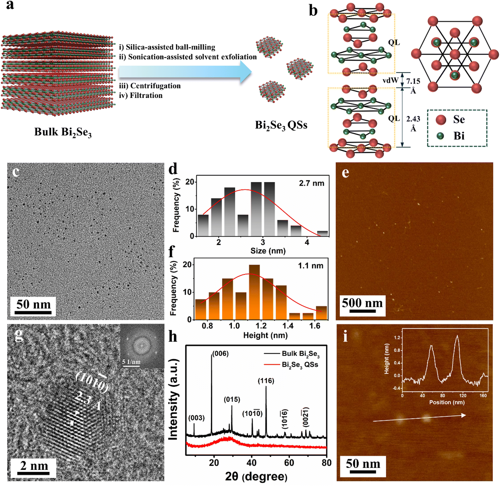 | ||
| Fig. 1 Scalable production and microscopic characterization of the Bi2Se3 QSs. (a) Schematic illustration of the fabrication process. (b) Schematic diagram of the crystal structure. (c) TEM image. (d) Corresponding lateral size distribution. (e) AFM image. (f) Corresponding height distribution. (g) HRTEM image (inset showing the corresponding FFT pattern). (h) XRD patterns. Data for bulk Bi2Se3 are shown for comparison. (i) High-magnification AFM image (inset showing the corresponding height profile). | ||
The crystal structure of the Bi2Se3 is schematically illustrated in Fig. 1(b), where the monolayer was constituted by five atomic layers. Multiple microscopic techniques were utilized for characterization of the Bi2Se3 QSs. Fig. 1 shows the corresponding transmission electron microscopy (TEM) and atomic force microscopy (AFM) images. The microscopic characterization of the Sb2Te3 QSs and TiS2 QSs can be found in Fig. S2 and S3 (ESI†). From Fig. 1(c), the Bi2Se3 QSs with uniform shapes and sizes were obtained. The average lateral sizes of 2.7, 3.2, and 1.9 nm were derived for Bi2Se3 QSs, Sb2Te3 QSs, and TiS2 QSs, respectively (Fig. 1(d) and Fig. S2, ESI†). Fig. 1(g) presents the high-resolution TEM (HRTEM) image and the corresponding fast Fourier transform (FFT) pattern of single Bi2Se3 QSs, indicating their single-crystalline structures. The lattice spacings of 0.23, 0.24, and 0.21 nm were revealed, corresponding to (10![[1 with combining macron]](https://www.rsc.org/images/entities/char_0031_0304.gif)
![[0 with combining macron]](https://www.rsc.org/images/entities/char_0030_0304.gif) ), (10), (102) crystal planes of Bi2Se3, Sb2Te3, and TiS2, respectively (Fig. 1(g) and Fig. S2, ESI†). The average heights of 1.1, 1.2, and 0.7 nm were derived for Bi2Se3 QSs, Sb2Te3 QSs, and TiS2 QSs, respectively (Fig. 1(e), (f) and Fig. S3, ESI†). The as-produced QSs were monolayers considering that the thicknesses of monolayer Bi2Se3, Sb2Te3, and TiS2 were approximately 1, 1, and 0.6 nm, respectively.18–20 Note that the individual height was acquired from the height profile of the single QS (Fig. 1(i)), which was the data source for the statistics in Fig. 1(f). Evidently, all the examined QSs were confirmed as quantum-sized monolayered structures.
), (10), (102) crystal planes of Bi2Se3, Sb2Te3, and TiS2, respectively (Fig. 1(g) and Fig. S2, ESI†). The average heights of 1.1, 1.2, and 0.7 nm were derived for Bi2Se3 QSs, Sb2Te3 QSs, and TiS2 QSs, respectively (Fig. 1(e), (f) and Fig. S3, ESI†). The as-produced QSs were monolayers considering that the thicknesses of monolayer Bi2Se3, Sb2Te3, and TiS2 were approximately 1, 1, and 0.6 nm, respectively.18–20 Note that the individual height was acquired from the height profile of the single QS (Fig. 1(i)), which was the data source for the statistics in Fig. 1(f). Evidently, all the examined QSs were confirmed as quantum-sized monolayered structures.
Multiple spectroscopic techniques were utilized for further characterization of the as-produced QSs. Fig. 1(h) and Fig. S5 (ESI†) show the X-ray diffraction (XRD) patterns of the QSs. From Fig. 1(h), the characteristic peaks at 9.3, 18.6, 29.4, 40.3, 47.7, 57.6 and 68.9° correspond to (003), (006), (015), (10), (116), (10![[6 with combining macron]](https://www.rsc.org/images/entities/char_0036_0304.gif) ) and (10
) and (10![[2 with combining macron]](https://www.rsc.org/images/entities/char_0032_0304.gif) ) crystal planes of Bi2Se3.21 From Fig. S5a (ESI†), the characteristic peaks at 8.7, 17.4, 26.3, 28.2, 38.3, 44.6, 54.2, 63.2, and 74.8° were assigned to (003), (006), (009), (015), (10), (10
) crystal planes of Bi2Se3.21 From Fig. S5a (ESI†), the characteristic peaks at 8.7, 17.4, 26.3, 28.2, 38.3, 44.6, 54.2, 63.2, and 74.8° were assigned to (003), (006), (009), (015), (10), (10![[5 with combining macron]](https://www.rsc.org/images/entities/char_0035_0304.gif) ), (10
), (10![[8 with combining macron]](https://www.rsc.org/images/entities/char_0038_0304.gif) ), (10) and (10
), (10) and (10![[4 with combining macron]](https://www.rsc.org/images/entities/char_0034_0304.gif) ) crystal planes of Sb2Te3.22 From Fig. S5b (ESI†), the characteristic peaks at 15.5, 31.3, 34.2, 44.1, 47.8, 53.7, 57.6 and 65.5° were indexed to (001), (002), (101), (012), (003), (110), (103) and (004) crystal planes of 1T-TiS2.23 Compared with bulk layered materials, the as-produced QSs were identified with significantly reduced crystallinity and extremely enhanced edge states. The Raman spectra of the QSs are shown in Fig. 2(a), (d) and (g), where the insets schematically displayed the typical Raman vibrational modes. For Bi2Se3, as shown in Fig. 2(a), three characteristic peaks were observed in bulk and QSs. The peaks at 130.5 cm−1 were assigned to Eg2 modes, whereas the peaks at 172.7 cm−1 corresponded to A1g2 modes.24 Compared with bulk Bi2Se3, the Bi2Se3 QSs showed the Eg2 modes and A1g2 modes with lower wavenumbers (i.e., 128.8 and 172.2 cm−1, respectively), which could be related to the relatively free states of vibrations in quantum-sized Bi2Se3.24 For Sb2Te3, as shown in Fig. 2(d), the peaks at 121.6 cm−1 were assigned to Eu2 modes, which could be infrared active.25 The peaks at 139.3 cm−1 were attributed to the vibrational modes of the Te–Te bonds26 and the peaks at 165.7 cm−1 were assigned to the A1g2 modes.25 Compared with bulk Sb2Te3, the Sb2Te3 QSs presented greatly suppressed and notably blue-shifted (128.7 cm−1) Eu2 modes. Such unconventional blue-shift might be caused by the possible change of the topological structure/state (e.g., electronic and vibrational properties) when transforming the bulk into QSs. On the one hand, the quantum confinement effects could alter the topological properties of the as-produced QSs. For instance, the time-reversal symmetry could be disrupted by external perturbations or confinement potentials, resulting in localization of electronic states.27 On the other hand, the geometric anisotropy of the as-produced QSs could affect the spin–orbit coupling of its surface/edge state, thus modifying the bulk-edge correspondence and the value of the topological invariant.28 The main reason for the blue-shift in Raman spectra could be attributed to the coupling between surface/edge states and bulk states, as well as the emerging localized states.29,30 For TiS2, as shown in Fig. 2(g), three characteristic peaks located at 149.2, 200.2, and 333.8 cm−1 were assigned to Eu, Eg, and A1g modes, respectively, consistent with those reported previously.31 Compared with bulk TiS2, the TiS2 QSs demonstrated quite weak Eu modes at 147.3 cm−1. The above-mentioned weakening of Raman signals could be originated from the extremely reduced lateral sizes and layer numbers when tailoring bulk layered materials into their QSs. The constituent elements and chemical states of the as-produced QSs were analyzed by X-ray photoelectron spectroscopy (XPS). Fig. S6 (ESI†) shows the XPS full spectra, where no impurities (e.g., Si from silica microspheres) were detected. Fig. 2(b), (c), (e), (f) and (h), (i) present the high-resolution XPS spectra, where both bulk and QSs were shown for comparison. For bulk Bi2Se3, as shown in Fig. 2(b) and (c), the two strong peaks at 158.2 and 163.5 eV corresponded to Bi 4f7/2 and Bi 4f5/2, while the two measured peaks at 53.6 and 54.4 eV were attributed to Se 3d5/2 and Se 3d3/2.32 For Bi2Se3 QSs, the Bi 4f peaks (159.7 eV for Bi 4f7/2 and 165.0 eV for Bi 4f5/2) and Se 3d peaks (55.2 eV for Se 3d5/2 and 56.3 eV for Se 3d3/2) all shifted towards higher binding energy by 1.5–1.9 eV. As reported previously,10 the extreme exposure of edge lattices/atoms in MoS2 QSs would result in the XPS peak shifting towards lower binding energy. Therefore, the as-observed opposite shifting of the XPS peaks could be driven by the possible change of the topological structure/state in Bi2Se3 QSs. Similar trends were found in Sb2Te3 QSs and TiS2 QSs. For bulk Sb2Te3, as shown in Fig. 2(e) and (f), the peaks at 528.6 and 538.0 eV were assigned to Sb 3d5/2 and Sb 3d3/2, while the peaks at 573.0 and 584.0 eV were attributed to Te 3d5/2 and Te 3d3/2. The probable oxidation of bulk Sb2Te3 led to the occurrence of the peaks at 530.4 eV for the Sb 3d5/2 and 539.8 eV for the Sb 3d3/2.33 For Sb2Te3 QSs, the Sb 3d peaks (530.7 eV for Sb 3d5/2 and 540.6 eV for Sb 3d3/2) and Te 3d peaks (577.1 eV for Te 3d5/2 and 588.8 eV for Te 3d3/2) shifted towards higher binding energy by 2.1–2.6 eV and 4.1–4.8 eV, respectively. For bulk TiS2, as shown in Fig. 2(h) and (i), the peaks of Ti 2p3/2 and Ti 2p1/2 were located at 456.3 and 462.5 eV. The two strong peaks at 160.9 and 162.1 eV corresponded to S 2p3/2 and S 2p1/2, consistent with those of 1T-TiS2.23 For TiS2 QSs, the Ti 2p peaks (459.2 eV for Ti 2p3/2 and 464.9 eV for Ti 2p1/2) shifted towards higher binding energy by 2.9 and 2.4 eV, respectively. The S 2p peaks shifted towards higher binding energy as well, although great suppression of the XPS signal was observed.
) crystal planes of Sb2Te3.22 From Fig. S5b (ESI†), the characteristic peaks at 15.5, 31.3, 34.2, 44.1, 47.8, 53.7, 57.6 and 65.5° were indexed to (001), (002), (101), (012), (003), (110), (103) and (004) crystal planes of 1T-TiS2.23 Compared with bulk layered materials, the as-produced QSs were identified with significantly reduced crystallinity and extremely enhanced edge states. The Raman spectra of the QSs are shown in Fig. 2(a), (d) and (g), where the insets schematically displayed the typical Raman vibrational modes. For Bi2Se3, as shown in Fig. 2(a), three characteristic peaks were observed in bulk and QSs. The peaks at 130.5 cm−1 were assigned to Eg2 modes, whereas the peaks at 172.7 cm−1 corresponded to A1g2 modes.24 Compared with bulk Bi2Se3, the Bi2Se3 QSs showed the Eg2 modes and A1g2 modes with lower wavenumbers (i.e., 128.8 and 172.2 cm−1, respectively), which could be related to the relatively free states of vibrations in quantum-sized Bi2Se3.24 For Sb2Te3, as shown in Fig. 2(d), the peaks at 121.6 cm−1 were assigned to Eu2 modes, which could be infrared active.25 The peaks at 139.3 cm−1 were attributed to the vibrational modes of the Te–Te bonds26 and the peaks at 165.7 cm−1 were assigned to the A1g2 modes.25 Compared with bulk Sb2Te3, the Sb2Te3 QSs presented greatly suppressed and notably blue-shifted (128.7 cm−1) Eu2 modes. Such unconventional blue-shift might be caused by the possible change of the topological structure/state (e.g., electronic and vibrational properties) when transforming the bulk into QSs. On the one hand, the quantum confinement effects could alter the topological properties of the as-produced QSs. For instance, the time-reversal symmetry could be disrupted by external perturbations or confinement potentials, resulting in localization of electronic states.27 On the other hand, the geometric anisotropy of the as-produced QSs could affect the spin–orbit coupling of its surface/edge state, thus modifying the bulk-edge correspondence and the value of the topological invariant.28 The main reason for the blue-shift in Raman spectra could be attributed to the coupling between surface/edge states and bulk states, as well as the emerging localized states.29,30 For TiS2, as shown in Fig. 2(g), three characteristic peaks located at 149.2, 200.2, and 333.8 cm−1 were assigned to Eu, Eg, and A1g modes, respectively, consistent with those reported previously.31 Compared with bulk TiS2, the TiS2 QSs demonstrated quite weak Eu modes at 147.3 cm−1. The above-mentioned weakening of Raman signals could be originated from the extremely reduced lateral sizes and layer numbers when tailoring bulk layered materials into their QSs. The constituent elements and chemical states of the as-produced QSs were analyzed by X-ray photoelectron spectroscopy (XPS). Fig. S6 (ESI†) shows the XPS full spectra, where no impurities (e.g., Si from silica microspheres) were detected. Fig. 2(b), (c), (e), (f) and (h), (i) present the high-resolution XPS spectra, where both bulk and QSs were shown for comparison. For bulk Bi2Se3, as shown in Fig. 2(b) and (c), the two strong peaks at 158.2 and 163.5 eV corresponded to Bi 4f7/2 and Bi 4f5/2, while the two measured peaks at 53.6 and 54.4 eV were attributed to Se 3d5/2 and Se 3d3/2.32 For Bi2Se3 QSs, the Bi 4f peaks (159.7 eV for Bi 4f7/2 and 165.0 eV for Bi 4f5/2) and Se 3d peaks (55.2 eV for Se 3d5/2 and 56.3 eV for Se 3d3/2) all shifted towards higher binding energy by 1.5–1.9 eV. As reported previously,10 the extreme exposure of edge lattices/atoms in MoS2 QSs would result in the XPS peak shifting towards lower binding energy. Therefore, the as-observed opposite shifting of the XPS peaks could be driven by the possible change of the topological structure/state in Bi2Se3 QSs. Similar trends were found in Sb2Te3 QSs and TiS2 QSs. For bulk Sb2Te3, as shown in Fig. 2(e) and (f), the peaks at 528.6 and 538.0 eV were assigned to Sb 3d5/2 and Sb 3d3/2, while the peaks at 573.0 and 584.0 eV were attributed to Te 3d5/2 and Te 3d3/2. The probable oxidation of bulk Sb2Te3 led to the occurrence of the peaks at 530.4 eV for the Sb 3d5/2 and 539.8 eV for the Sb 3d3/2.33 For Sb2Te3 QSs, the Sb 3d peaks (530.7 eV for Sb 3d5/2 and 540.6 eV for Sb 3d3/2) and Te 3d peaks (577.1 eV for Te 3d5/2 and 588.8 eV for Te 3d3/2) shifted towards higher binding energy by 2.1–2.6 eV and 4.1–4.8 eV, respectively. For bulk TiS2, as shown in Fig. 2(h) and (i), the peaks of Ti 2p3/2 and Ti 2p1/2 were located at 456.3 and 462.5 eV. The two strong peaks at 160.9 and 162.1 eV corresponded to S 2p3/2 and S 2p1/2, consistent with those of 1T-TiS2.23 For TiS2 QSs, the Ti 2p peaks (459.2 eV for Ti 2p3/2 and 464.9 eV for Ti 2p1/2) shifted towards higher binding energy by 2.9 and 2.4 eV, respectively. The S 2p peaks shifted towards higher binding energy as well, although great suppression of the XPS signal was observed.
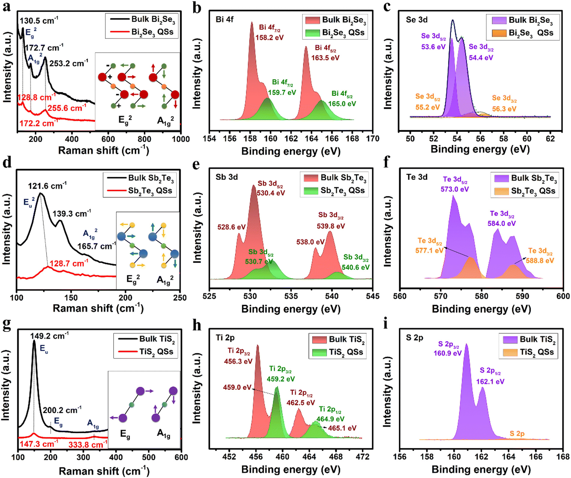 | ||
| Fig. 2 Spectroscopic characterization of the as-produced QSs. Raman spectra of (a) Bi2Se3 QSs, (d) Sb2Te3 QSs, and (g) TiS2 QSs. High-resolution XPS spectra of (b), (c) Bi2Se3 QSs, (e), (f) Sb2Te3 QSs, and (h), (i) TiS2 QSs. Data for bulk materials are shown for comparison. | ||
The optical properties of the as-produced QSs were investigated, as shown in Fig. 3 and Fig. S7–S11 (ESI†). Fig. 3(a)–(c) present the excitation wavelength-, concentration-, and solvent-dependent PL behavior of the Bi2Se3 QS dispersions. A similar phenomenon could be found in the Sb2Te3 and TiS2 QS dispersions (Fig. S8–S10, ESI†). From Fig. 3(a), the PL intensity reached the maximum at the excitation wavelength of 360 nm for the Bi2Se3 QS dispersions. Such excitation wavelength-dependent PL behavior could be attributed to the size/thickness heterogeneity of the 2D QSs.8Fig. 3(b) shows the concentration-dependent PL behavior of the Bi2Se3 QS dispersions. The PL intensity was progressively enhanced with the concentration from 0.001 to 0.025 mg mL−1 because of the increase of the PL emitters. However, the PL intensity started to decrease with the concentration from 0.025 to 1 mg mL−1, which could be ascribed to the aggregation-caused quenching (ACQ) mechanism.8,34–36Fig. 3(c) presents the solvent-dependent PL behavior of the Bi2Se3 QS dispersions. The PL intensity of the QS dispersions in varying solvents showed remarkable difference, which could be determined by QS-solvent (direct) interactions.8,37,38 The PL lifetimes and quantum yields of the QSs were measured, as shown in Fig. 3(d) and Fig. S11 (ESI†). The PL lifetimes of Bi2Se3, Sb2Te3, and TiS2 QSs were measured to be approximately 6.6, 7.0, and 3.1 ns, respectively. The absolute quantum yields were measured to be 4.9, 3.6, and 6.3% for the Bi2Se3, Sb2Te3, and TiS2 QSs at the wavelength of 360, 360 and 380 nm, respectively. It should be noted that all the examined QSs exhibited blue PL, which could be determined by their bandgaps. The optical bandgaps were derived from the UV-vis absorption spectra, as shown in Fig. S7 (ESI†). Fig. 3(e) compares the optical bandgaps between bulk and QSs. For Bi2Se3, Sb2Te3, and TiS2, with the sizes down to 2.7, 3.2, and 1.9 nm, the bandgaps increased to 4.72, 4.69, and 3.59 eV, much larger than those (e.g., 0.22, 0.22, 0.30 eV) of bulk materials.39–41 The as-produced QSs with extremely reduced thickness and lateral size would cause strong (out-of-plane and in-plane) quantum confinement effects, resulting in significant broadening of the optical bandgaps.42,43 The bandgaps matched well with the blue emission of the QSs. Such (significant) bandgap-widening by (extreme) size-reduction would facilitate the practical applications of the topological insulators and semimetals.
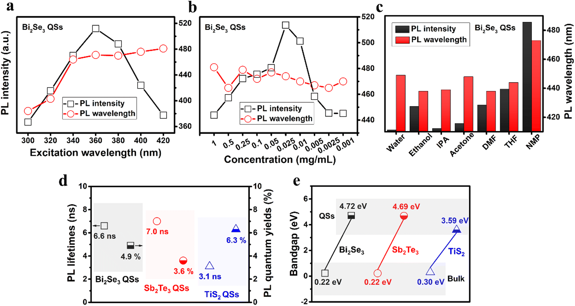 | ||
| Fig. 3 Photoluminescence of the QS dispersions. (a) Excitation wavelength-dependent PL behavior. (b) Concentration-dependent PL behavior. (c) Solvent-dependent PL behavior. (d) PL lifetimes and quantum yields. (e) Optical bandgap-modulation by size-reduction. | ||
Not only linear but also nonlinear optical performances of the as-produced QSs were explored. Fig. 4(a) shows the schematic setup for the NSA measurements. The laser pulse with wavelengths of 532 and 800 nm, duration of 100 fs, and repetition rate of 1 kHz was incident on an aperture of diameter 4 mm. Fig. S12a (ESI†) presents the photographs of the pure PMMA and QSs-PMMA thin films (with the thickness of 120 μm and the edge length of 1 cm). The QSs-PMMA thin films with the fixed loading content of 0.1 wt% demonstrated slightly lower transparency than that of the pure PMMA, further confirmed by UV-vis absorption spectroscopy (Fig. S12b, ESI†). Such high transparency would be the basic requirement for future applications. Note that there was no detectable aggregation/orientation of the QSs in the hybrid thin films, which was determined by the thermodynamic stability of such dispersions.8 The NSA curves of the QSs-PMMA thin films are shown in Fig. S12c, d and S13 (ESI†). The normalized NSA curves (Fig. S13a and b, ESI†) were well fitted by the following formula: 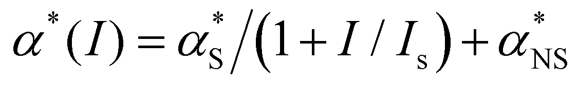 44 where α*(I) is the absorption coefficient,
  and
and  are the saturable and nonsaturable absorption components, I is the peak intensity (or power density) of the incident pulsed laser, and Is is the saturation intensity defined as the optical intensity required in a steady state to reduce the absorption to half of its unbleached value. Fig. 4(b) summarizes the as-acquired NSA performances of the Bi2Se3, Sb2Te3, and TiS2 QSs-PMMA thin films. From Fig. 4(b), unprecedented NSA performances were achieved in the QSs-PMMA thin films at wavelengths of both 532 and 800 nm. At 532 nm, the absolute modulation depths of 71.6, 45.1, and 43.6% as well as the saturation intensities of 1.52, 0.82, and 1.53 MW cm−2 (i.e., 152, 82, and 153 nJ cm−2) were derived for the Bi2Se3 QSs-PMMA, Sb2Te3 QSs-PMMA, and TiS2 QSs-PMMA, respectively. At 800 nm, the absolute modulation depths of 72.4, 55.2, and 68.4% as well as the saturation intensities of 0.49, 0.34, and 0.80 MW cm−2 (i.e., 49, 34, and 80 nJ cm−2) were achieved for the Bi2Se3 QSs-PMMA, Sb2Te3 QSs-PMMA, and TiS2 QSs-PMMA, respectively. Note that the Bi2Se3 QSs-PMMA retained extremely high NSA performances in the visible region, while the Sb2Te3 QSs-PMMA and TiS2 QSs-PMMA demonstrated wavelength-dependent NSA performances. In addition, the TiS2 QSs-PMMA showed comparable NSA performances to those of the Bi2Se3 QSs-PMMA at 800 nm, indicating the great potential in both topological insulators and semimetals. Besides the absolute modulation depths and saturation intensities, the relative modulation depths (i.e.,
  ) and nonsaturable losses (i.e.,
  ) were derived, as shown in Fig. S13 (ESI†). All the examined QSs presented high
  and satisfactory
  . Particularly, the Bi2Se3 QSs-PMMA demonstrated ultrahigh
  of 95.9% and extremely low
  of 4.1%, further supporting its extraordinary NSA performances. Table S1 (ESI†) lists the NSA performances of the as-produced QSs and the topological insulators/semimetals from other works. Based on Table S1 (ESI†), the complete comparison of their NSA performances (i.e., the absolute modulation depths and saturation intensities) was accomplished, as shown in Fig. 4(c) and (d). Excitingly, ultrahigh nonlinear response and ultralow power excitation were simultaneously achieved in the as-produced QSs. Meanwhile, the Bi2Se3 QSs-PMMA demonstrated record-high absolute modulation depth (72.4% at 800 nm), which had never been achieved before (not limited to topological insulators/semimetals). Such extraordinary NSA performances of the as-fabricated QSs-PMMA thin films could originate from three aspects: (1) the inherent characteristics of the material; (2) intrinsic edge effects; and (3) quantum confinement effect. Firstly, topological insulator/semimetal were a novel state of quantum matter with an insulating bulk state and gapless surface/edge states.45,46 The unique electronic structure at the surface/edge states of the topological insulator/semimetal made it different from the traditional saturable absorbers (such as graphene, hexagonal boron nitride, transition metal dichalcogenides, In2X3(X = S, Se, Te), MXene) thus exhibited higher NSA performances.8,9,47,48 Therefore, the inherent characteristics of topological insulator/semimetal played an important role in the NSA performances. Secondly, the as-produced QSs possessed entirely exposed edges, maximizing their intrinsic edge effects (nonequilibrium situation (e.g., broken lattices, unsaturated/dangling bonds, dynamic changes, etc.) and asymmetric environment). The lattice at the surfaces/edges would dominate compared with their internal lattice in the as-produced QSs. The key roles of the rich surface/edge electronic states on the NSA performances included two aspects: (1) the unique density of states leaded to a strong overlap between the electronic wavefunctions and incident photons, resulting in an enhanced light–matter interaction. Such interaction facilitated the absorption of the incident light; and (2) the surface/edge electronic states of the as-produced QSs were topologically protected, indicating that they were robust against disorders and perturbations. The robustness of the surface/edge states ensured their effective nonlinear saturation absorption. Hence, the surface/edge (free, nonequilibrium) electronic states played a significant role in their absorption of photons.49 Thirdly, the extreme size-reduction in the QSs would induce (both in-plane and out-of-plane) quantum confinement effects. Such effects would change the electronic structure, exciton properties and density of states of the as-produced QSs, directly affecting the changes of its nonlinear absorption coefficient, saturation intensity and excited state dynamics, resulting in ultrahigh saturable absorption.50–52 Evidently, the combination of the inherent characteristics of the material, quantum confinement and intrinsic edge effects could be determinative to their phenomenal NSA performances of the quantum-sized topological insulators and semimetals.
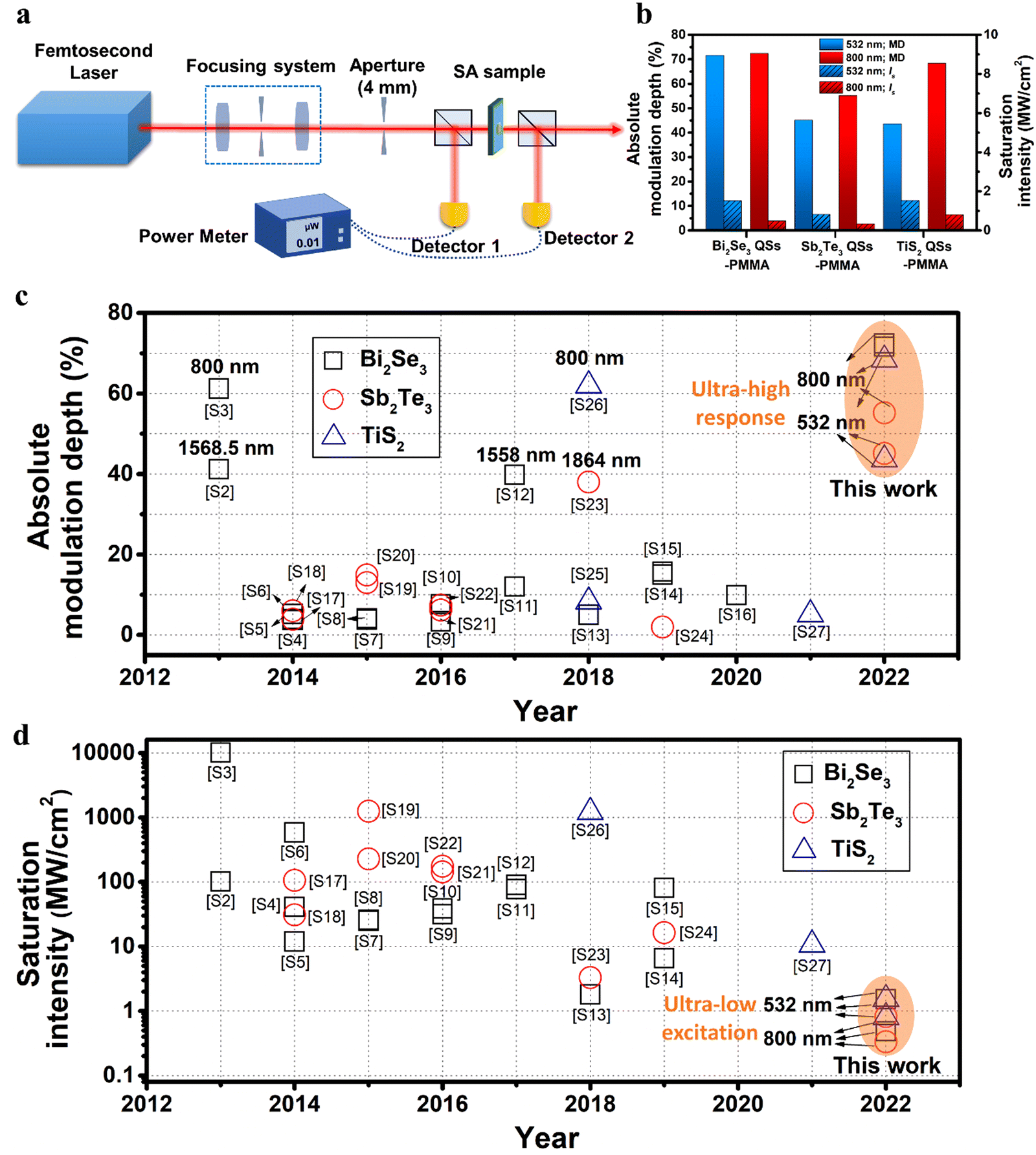 | ||
| Fig. 4 NLO performances of the QS solid thin films. (a) Schematic setup of the NSA measurement. (b) Plots of the absolute modulation depth and saturation intensity. (c) and (d) NSA performance comparison in topological insulators/semimetals. The references (S2–S27) are listed in Table S1 and the ESI.† | ||
3. Conclusions
In summary, quantum-sized topological insulators/semimetals (i.e., Bi2Se3 QSs, Sb2Te3 QSs, and TiS2 QSs) were produced via an all-physical top-down method. The as-produced QSs were monolayers with intrinsic characteristics, which could be determinative to their extraordinary performances. The highly stable QS dispersions presented excitation wavelength-, concentration-, and solvent-dependent PL. The highly transparent QSs-PMMA thin films demonstrated broadband NSA in the visible. Ultrahigh nonlinear response (72.4 and 68.4%) and ultralow power excitation (0.49 and 0.80 MW cm−2) were simultaneously achieved in both Bi2Se3 QSs-PMMA and TiS2 QSs-PMMA. Compared with TiS2 QSs-PMMA, Bi2Se3 QSs-PMMA maintained extremely high NSA performance at varying (laser) wavelength (532 and 800 nm). Such a highly desired broadband feature in quantum-sized topological insulators would undoubtedly facilitate their applications in mode-locked lasers and related fields.Author contributions
Z. C. performed the experiments and characterization studies. Y. Z. supervised the research project. Y. Z. and Z. C. analyzed the data and wrote the manuscript. Z. L. and Y. L. helped with the spectroscopic characterization. X. S. and X. L. performed the nonlinear optical characterization.Conflicts of interest
The authors declare no conflict of interest.Acknowledgements
This work was supported by the National Natural Science Foundation of China (no. 52073070, 21673054, 11874130, and 22073022), the Strategic Priority Research Program of Chinese Academy of Sciences (no. XDB36000000), the National Key R&D Program of China (no. 2018YFA0703700), and the DNL Cooperation Fund CAS (DNL202016).References
- K. S. Novoselov, A. K. Geim, S. V. Morozov, D. Jiang, Y. Zhang, S. V. Dubonos, I. V. Grigorieva and A. A. Firsov, Electric field effect in atomically thin carbon films, Science, 2004, 306, 666–669 CrossRef CAS PubMed.
- A. K. Geim, Graphene: Status and prospects, Science, 2009, 324, 1530–1534 CrossRef CAS PubMed.
- Q. L. He, T. L. Hughes, N. P. Armitage, Y. Tokura and K. L. Wang, Topological spintronics and magnetoelectronics, Nat. Mater., 2022, 21, 15–23 CrossRef CAS PubMed.
- A. A. Burkov, Topological semimetals, Nat. Mater., 2016, 15, 1145–1148 CrossRef CAS PubMed.
- M. Z. Hasan and C. L. Kane, Colloquium: Topological insulators, Rev. Mod. Phys., 2010, 82, 3045–3067 CrossRef CAS.
- A. Wang, X. Ye, D. Yu and Z. Liao, Topological semimetal nanostructures: From properties to topotronics, ACS Nano, 2020, 14, 3755–3778 CrossRef CAS PubMed.
- O. Breunig and Y. Ando, Opportunities in topological insulator devices, Nat. Rev. Phys., 2022, 4, 184–193 CrossRef.
- Y. Xu, S. Chen, Z. Dou, Y. Ma, Y. Mi, W. Du, Y. Liu, J. Zhang, J. Chang, C. Liang, J. Zhou, H. Guo, P. Gao, X. Liu, Y. Che and Y. Zhang, Robust production of 2D quantum sheets from bulk layered materials, Mater. Horiz., 2019, 6, 1416–1424 RSC.
- C. Han, Y. Zhang, P. Gao, S. Chen, X. Liu, Y. Mi, J. Zhang, Y. Ma, W. Jiang and J. Chang, High-yield production of MoS2 and WS2 quantum sheets from their bulk materials, Nano Lett., 2017, 17, 7767–7772 CrossRef CAS PubMed.
- C. Liang, X. Sui, A. Wang, J. Chang, W. Wang, Z. Chen, W. Jiang, Y. Ma, J. Zhang, X. Liu and Y. Zhang, Controlled production of MoS2 full-scale nanosheets and their strong size effects, Adv. Mater. Interfaces, 2020, 7, 2001130 CrossRef CAS.
- Y. Xu, J. Chang, C. Liang, X. Sui, Y. Ma, L. Song, W. Jiang, J. Zhou, H. Guo, X. Liu and Y. Zhang, Tailoring multi-walled carbon nanotubes into graphene quantum sheets, ACS Appl. Mater. Interfaces, 2020, 12, 47784–47791 CrossRef CAS PubMed.
- Y. Xu, W. Wang, Z. Chen, X. Sui, A. Wang, C. Liang, J. Chang, Y. Ma, L. Song, W. Jiang, J. Zhou, X. Liu and Y. Zhang, A general strategy for semiconductor quantum dot production, Nanoscale, 2021, 13, 8004–8011 RSC.
- Z. Chen, W. Wang, X. Sui, K. Wang, J. Zhang, X. Liu and Y. Zhang, Quantum-sized silicon for enhanced photoluminescence and optical nonlinearity, Mater. Chem. Front., 2021, 5, 7817–7823 RSC.
- V. V. Zubyuk, P. P. Vabishchevich, M. R. Shcherbakov, A. S. Shorokhov, A. N. Fedotova, S. Liu, G. Keeler, T. V. Dolgova, I. Staude, I. Brener and A. A. Fedyanin, Low-power absorption saturation in semiconductor metasurfaces, ACS Photonics, 2019, 6, 2797–2806 CrossRef CAS.
- G. Wang, A. A. Baker-Murray and W. J. Blau, Saturable absorption in 2D nanomaterials and related photonic devices, Laser Photonics Rev., 2019, 13, 1800282 CrossRef.
- X. Liu, Q. Guo and J. Qiu, Emerging low-dimensional materials for nonlinear optics and ultrafast photonics, Adv. Mater., 2017, 29, 1605886 CrossRef PubMed.
- Y. Ge, Z. Zhu, Y. Xu, Y. Chen, S. Chen, Z. Liang, Y. Song, Y. Zou, H. Zeng, S. Xu, H. Zhang and D. Fan, Broadband nonlinear photoresponse of 2D TiS2 for ultrashort pulse generation and all-optical thresholding devices, Adv. Opt. Mater., 2018, 6, 1701166 CrossRef.
- A. I. Komonov, V. Y. Prinz, V. A. Seleznev, K. A. Kokh and V. N. Shlegel, Step-height standards based on the rapid formation of monolayer steps on the surface of layered crystals, Appl. Surf. Sci., 2017, 410, 1–7 CrossRef CAS.
- M. Xia, K. Ding, F. Rao, X. Li, L. Wu and Z. Song, Aluminum-centered tetrahedron-octahedron transition in advancing Al–Sb–Te phase change properties, Sci. Rep., 2015, 5, 8548 CrossRef CAS PubMed.
- Z. Gao, Q. Ji, P.-C. Shen, Y. Han, W. S. Leong, N. Mao, L. Zhou, C. Su, J. Niu, X. Ji, M. M. Goulamaly, D. A. Muller, Y. Li and J. Kong, In situ-generated volatile precursor for CVD growth of a semimetallic 2D dichalcogenide, ACS Appl. Mater. Interfaces, 2018, 10, 34401–34408 CrossRef CAS PubMed.
- H. Lai, S. Jian, L. T. C. Tuyen, P. H. Le, C. Luo and J. Juang, Nanoindentation of Bi2Se3 thin films, Micromachines, 2018, 9, 518 CrossRef PubMed.
- B. Lv, S. Hu, W. Li, X. Di, L. Feng, J. Zhang, L. Wu, Y. Cai, B. Li and Z. Lei, Preparation and characterization of Sb2Te3 thin films by coevaporation, Int. J. Photoenergy, 2010, 2010, 476589 CrossRef.
- Y. Liu, C. Liang, J. Wu, T. Sharifi, H. Xu, Y. Nakanishi, Y. Yang, C. F. Woellne, A. Aliyan, A. A. Martí, B. Xie, R. Vajtai, W. Yang and P. M. Ajayan, Atomic layered titanium sulfide quantum dots as electrocatalysts for enhanced hydrogen evolution reaction, Adv. Mater. Interfaces, 2018, 5, 1700895 CrossRef.
- J. Zhang, Z. Peng, A. Soni, Y. Zhao, Y. Xiong, B. Peng, J. Wang, M. S. Dresselhaus and Q. Xiong, Raman spectroscopy of few-quintuple layer topological insulator Bi2Se3 nanoplatelets, Nano Lett., 2011, 11, 2407–2414 CrossRef CAS PubMed.
- K. Norimatsu, M. Hada, S. Yamamoto, T. Sasagawa, M. Kitajima, Y. Kayanuma and K. G. Nakamura, Dynamics of all the Raman-active coherent phonons in Sb2Te3 revealed via transient reflectivity, J. Appl. Phys., 2015, 117, 143102 CrossRef.
- S. A. Nemov, V. D. Andreeva, Y. V. Ulashkevich, A. V. Povolotsky and A. A. Allahkhah, Specific features of the IR reflectance and Raman spectra of Sb2Te3−xSex crystals, Semiconductors, 2018, 52, 1317–1322 CrossRef CAS.
- M. S. Bahramy, P. D. C. King, A. de la Torre, J. Chang, M. Shi, L. Patthey, G. Balakrishnan, P. Hofmann, R. Arita, N. Nagaosa and F. Baumberger, Emergent quantum confinement at topological insulator surfaces, Nat. Commun., 2012, 3, 1159 CrossRef CAS PubMed.
- H. Kurebayashi, J. H. Garcia, S. Khan, J. Sinova and S. Roche, Magnetism, symmetry and spin transport in van der Waals layered systems, Nat. Rev. Phys., 2022, 4, 150–166 CrossRef CAS.
- H. H. Kung, M. Salehi, I. Boulares, A. F. Kemper, N. Koirala, M. Brahlek, P. Lošťák, C. Uher, R. Merlin, X. Wang, S. W. Cheong, S. Oh and G. Blumberg, Surface vibrational modes of the topological insulator Bi2Se3 observed by Raman spectroscopy, Phys. Rev. B, 2017, 95, 245406 CrossRef.
- H. Padmanabhan, M. Poore, P. K. Kim, N. Z. Koocher, V. A. Stoica, D. Puggioni, H. Wang, X. Shen, A. H. Reid, M. Gu, M. Wetherington, S. H. Lee, R. D. Schaller, Z. Mao, A. M. Lindenberg, X. Wang, J. M. Rondinelli, R. D. Averitt and V. Gopalan, Interlayer magnetophononic coupling in MnBi2Te4, Nat. Commun., 2022, 13, 1929 CrossRef CAS PubMed.
- X. Zhu, S. Chen, M. Zhang, L. Chen, Q. Wu, J. Zhao, Q. Jiang, Z. Zheng and H. Zhang, TiS2-based saturable absorber for ultrafast fiber lasers, Photonics Res., 2018, 6, C44–C48 CrossRef CAS.
- C. Liu, H. Zhang, Z. Sun, K. Ding, J. Mao, Z. Shao and J. Jie, Topological insulator Bi2Se3 nanowire/Si heterostructure photodetectors with ultrahigh responsivity and broadband response, J. Mater. Chem. C, 2016, 4, 5648–5655 RSC.
- J. Schaumann, M. Loor, D. Ünal, A. Mudring, S. Heimann, U. Hagemann, S. Schulz, F. Maculewicz and G. Schierning, Improving the zT value of thermoelectrics by nanostructuring: tuning the nanoparticle morphology of Sb2Te3 by using ionic liquids, Dalton Trans., 2017, 46, 656–668 RSC.
- Y. Hong, J. W. Y. Lam and B. Tang, Aggregation-induced emission: phenomenon, mechanism and applications, Chem. Commun., 2009, 4332–4353 RSC.
- W. Z. Yuan, P. Lu, S. Chen, J. W. Y. Lam, Z. Wang, Y. Liu, H. S. Kwok, Y. Ma and B. Z. Tang, Changing the behavior of chromophores from aggregation-caused quenching to aggregation-induced emission: Development of highly efficient light emitters in the solid state, Adv. Mater., 2010, 22, 2159–2163 CrossRef CAS PubMed.
- L. Cao, M. J. Meziani, S. Sahu and Y. P. Sun, Photoluminescence properties of graphene versus other carbon nanomaterials, Acc. Chem. Res., 2013, 46, 171–180 CrossRef CAS PubMed.
- C. Wang, L. Zhang, J. Wang, S. Su, X. Jin, P. An, B. Sun and Y. Luo, Ultra-thin two-dimensional nanosheets for in-situ NIR light-triggered fluorescence enhancement, FlatChem, 2020, 24, 100193 CrossRef CAS.
- H. Jin, B. Baek, D. Kim, F. Wu, J. D. Batteas, J. Cheon and D. H. Son, Effects of direct solvent-quantum dot interaction on the optical properties of colloidal monolayer WS2 quantum dots, Nano Lett., 2017, 17, 7471–7477 CrossRef CAS PubMed.
- G. Martinez, B. A. Piot, M. Hakl, M. Potemski, Y. S. Hor, A. Materna, S. G. Strzelecka, A. Hruban, O. Caha, J. Novák, A. Dubroka, Č. Drašar and M. Orlita, Determination of the energy band gap of Bi2Se3, Sci. Rep., 2017, 7, 6891 CrossRef CAS PubMed.
- A. Lawal, A. Shaari, R. Ahmed and N. Jarkoni, Sb2Te3 crystal a potential absorber material for broadband photodetector: A first-principles study, Results Phys., 2017, 7, 2302–2310 CrossRef.
- C. Weng, Y. Luo, B. Wang, J. Shi, L. Gao, Z. Cao and G. Duan, Layer-dependent SERS enhancement of TiS2 prepared by simple electrochemical intercalation, J. Mater. Chem. C, 2020, 8, 14138–14145 RSC.
- Z. X. Gan, L. Z. Liu, H. Y. Wu, Y. L. Hao, Y. Shan, X. L. Wu and P. K. Chu, Quantum confinement effects across two-dimensional planes in MoS2 quantum dots, Appl. Phys. Lett., 2015, 106, 233113 CrossRef.
- Y. Wang, Y. Liu, J. Zhang, J. Wu, H. Xu, X. Wen, X. Zhang, C. S. Tiwary, W. Yang, R. Vajtai, Y. Zhang, N. Chopra, I. N. Odeh, Y. Wu and P. M. Ajayan, Cryo-mediated exfoliation and fracturing of layered materials into 2D quantum dots, Sci. Adv., 2017, 3, e1701500 CrossRef PubMed.
- Q. Bao, H. Zhang, Y. Wang, Z. Ni, Y. Yan, Z. Shen, K. P. Loh and D. Tang, Atomic-layer graphene as a saturable absorber for ultrafast pulsed lasers, Adv. Funct. Mater., 2009, 19, 3077–3083 CrossRef CAS.
- B. A. Bernevig, T. L. Hughes and S. C. Zhang, Quantum spin hall effect and topological phase transition in HgTe quantum wells, Science, 2006, 314, 1757–1761 CrossRef CAS PubMed.
- J. E. Moore, The birth of topological insulators, Nature, 2010, 464, 194–198 CrossRef CAS PubMed.
- W. Wang, Z. Chen, X. Sui, Y. Li, X. Liu and Y. Zhang, Phase/size dual controlled 2D semiconductor In2X3 (X = S, Se, Te) for saturable absorption modulation, Nano Res., 2022, 15, 5633–5639 CrossRef CAS.
- Z. Chen, X. Sui, Y. Li, X. Liu and Y. Zhang, Ti3AlC2 MAX and Ti3C2 MXene quantum sheets for record-high optical nonlinearity. J. Phys, Chem. Lett., 2022, 13, 3929–3936 CAS.
- X. Zhang, J. Wang and S. Zhang, Topological insulators for high-performance terahertz to infrared applications, Phys. Rev. B: Condens. Matter Mater. Phys., 2010, 82, 245107 CrossRef.
- Q. Gao, Y. Peng, T. Wang, C. Shen, C. Xia, J. Yang and Z. Wei, Quantum confinement effects on excitonic properties in the 2D vdW quantum system: The ZnO/WSe2 case, Adv. Photonics Res., 2021, 2, 2000114 CrossRef CAS.
- S. Haldar, V. K. Dixit, G. Vashisht, S. K. Khamari, S. Porwal, T. K. Sharma and S. M. Oak, Effect of carrier confinement on effective mass of excitons and estimation of ultralow disorder in AlxGa1−xAs/GaAs quantum wells by magneto-photoluminescence, Sci. Rep., 2017, 7, 4905 CrossRef CAS PubMed.
- N. P. Wilson, W. Yao, J. Shan and X. Xu, Excitons and emergent quantum phenomena in stacked 2D semiconductors, Nature, 2021, 599, 383–392 CrossRef CAS PubMed.
Footnote |
| † Electronic supplementary information (ESI) available. See DOI: https://doi.org/10.1039/d3nh00282a |
| This journal is © The Royal Society of Chemistry 2023 |