
Two dimensional NbSe2/Nb2O5 metal–semiconductor heterostructure-based photoelectrochemical photodetector with fast response and high flexibility†
Xiang
Xu‡
*a,
Chunhui
Lu‡
b,
Ying
Wang
a,
Xing
Bai
a,
Zenghui
Liu
a,
Ying
Zhang
a and
Dengxin
Hua
a
aSchool of Mechanical and Precision Instrument Engineering, Xi’an University of Technology, Xi’an 710048, China. E-mail: xxuxxiang@xaut.edu.cn; Tel: +86 15529500771
bInstitute of Photonics & Photon-Technology, School of Physics, Northwest University, Xi’an 710069, China
First published on 2nd June 2023
Abstract
Two dimensional (2D) metal-semiconductor heterostructures are promising for high-performance optoelectronic devices due to fast carrier separation and transportation. Considering the superior metallic characteristics accompanied by high electrical conductivity in NbSe2, surface oxidation provides a facile way to form NbSe2/Nb2O5 metal-semiconductor heterostructures. Herein, size-dependent NbSe2/Nb2O5 nanosheets were achieved by a liquid phase exfoliation method and a gradient centrifugation strategy. These NbSe2/Nb2O5 heterostructure-based photodetectors show high responsivity with 23.21 μA W−1, fast response time of millisecond magnitude, and wide band detection ability in the UV-Vis region. It is noticeable that the photocurrent density is sensitive to the surface oxygen layer due to the oxygen-sensitized photoconduction mechanism. The flexible testing of the NbSe2/Nb2O5 heterostructure-based PEC-type photodetectors exhibits high photodetection performance even after bending and twisting. Beyond that, the solid-state PEC-type NbSe2/Nb2O5 photodetector also achieves relatively stable photodetection and high stability. This work promotes the application of 2D NbSe2/Nb2O5 metal-semiconductor heterostructures in flexible optoelectronic devices.
New conceptsConsidering the superior metallic characteristics accompanied by high electrical conductivity in NbSe2, surface oxidation provides an efficient way to form NbSe2/Nb2O5 metal-semiconductor heterostructures (MSHSs). We aim to explore the photodetection performance of the size-dependent NbSe2/Nb2O5 MSHSs. In this work, we demonstrate that this NbSe2/Nb2O5 based photoelectrochemical (PEC) photodetector shows high responsivity, fast response time of millisecond magnitude, and wide band detection ability in the UV-Vis region. Additionally, this NbSe2/Nb2O5 exhibits high photodetection performance even after flexible testing. Furthermore, the solid-state PEC-type NbSe2/Nb2O5 photodetector also achieves relatively stable photodetection. This work provides an opportunity to synthesize 2D metal-semiconductor heterostructures, which have great potential for designing high-performance PEC-type photodetector applications. |
Introduction
Two dimensional (2D) transition metal dichalcogenides (TMDs) have been widely designed for high-performance flexible optoelectronic devices due to their unique physical, chemical, and mechanical properties.1,2 Among them, semiconducting layered TMD materials especially, MoX2 or WX2 (X = S or Se), show a tunable band gap with layer number,3 stronger light-absorption compared with traditional Si and GaAs,4 and high solar energy conversion beyond 10%.5 Accordingly, 2D semiconducting layered TMDs have been widely investigated and applied in optoelectronic applications.6,7 Besides, 2D TMD-based semiconductor–semiconductor and semiconductor-insulator heterostructures have also been widely studied in both theory and experiments, because these heterostructures show novel physical phenomena and great potential in photovoltaic, optoelectronic, and energy storage devices.8–10 However, their optoelectronic performance is strongly hindered due to the poor electrode contact. Recently, theoretical calculations have demonstrated that 2D metal-semiconductor heterostructures (MSHSs) not only weaken the Fermi level pinning, but also modulate the Schottky barrier. Although some MSHSs are reported, most of the studies focus on graphene-based MSHSs due to the limited 2D metallic materials. With the advancement of current industrial applications, metallic TMDs have been successfully synthesized and widely reported. As members of the metallic TMDs, TaSe2, NbSe2, and TaS2 are mainly investigated in superconductivity11,12 and the charge density wave phenomenon.13 These metallic TMDs show no band gap and high electrical conductivity,14,15 and have a great potential for good electrode contact in a 2D semiconductor device. NbSe2, a representative of metallic TMDs, becomes a type II superconductor under 7.2 K.16 Moreover, the metallic nature endows outstanding electronic transport ability. As such, it is promising to be an electrical contact and connect with semiconductors, forming metal-semiconductor heterostructures (MSHSs).17,18 The experimental realization of NbSe2-based MSHSs has demonstrated a high carrier mobility and reduced contact resistance.19,20 Even though a few MSHSs have great potential in integrated electronics, the large-area synthesis is still a great challenge.Surface oxidation is an easy and efficient way to construct heterostructures and tailor the performance of optoelectronic devices.21 A thin oxidation layer was introduced as In2O3/InSe22 and WOx/WSe2,23 which can adjust the band edge positions and improve the performance of the photodetector. Considering poor stability of NbSe2, surface oxidation treatment is easy to form the NbSe2/Nb2O5 heterostructure24 as exposed to air. Nb2O5 shows strong stability in an aqueous medium, a band gap of 3.4 eV and high light absorption in the UV region.25,26 The heterostructure constructed with metallic NbSe2, serving as an electrode contact, exhibits a higher mobility and markedly improves the charge transfer efficiency in the mixed NbSe2/Nb2O5 heterostructure. The formation of the NbSe2/Nb2O5 heterostructure renders it a promising candidate for semiconductor electronic and photodetector applications. It is well known that the solvent-assisted exfoliation technique can not only obtain 2D NbSe2 nanosheet dispersions but also introduce the surface oxidation by size-separation.24,27–30 This provides an opportunity to design NbSe2/Nb2O5 MSHS based photodetectors and investigate the photoelectric properties. Different from field effect transistor (FET)-based photodetectors, photoelectrochemical (PEC)-type photodetectors act as a new functional photodetection system to detect the conversion of light-electric signals.31–35 There are some inherent advantages: (i) easy to adjust in terms of photoelectric performance by light intensity and bias voltage; (ii) simple and low-cost measurement procedure; (iii) close-knit electrical contact to the sample between the redox electrolyte and solid electrode; (iv) efficient perpendicular charge separation and transport pathways. In this context, NbSe2/Nb2O5 MSHS is expected to be applied into PEC-type photodetectors, which has not been reported yet to the best of our knowledge.
Herein, NbSe2/Nb2O5 metal-semiconductor heterostructures were achieved by a solvent-assisted exfoliation technique with a gradient centrifugation method, and were characterized by transmission electron microscopy (TEM), scanning electron microscopy (SEM), X-ray diffraction (XRD), X-ray photoelectron spectroscopy (XPS) and atomic force microscopy (AFM). The NbSe2/Nb2O5 MSHS-based PEC-type photodetector shows high responsivity, fast response time and recovery time, and wide band detection. It is worth pointing out that the sensitivity of the photocurrent density to ambient conditions is due to the oxygen-sensitized photoconduction mechanism. Furthermore, the NbSe2/Nb2O5 PEC-type photodetector still exhibits high photodetection performance and high flexibility even after bending and twisting approximately 300 cycles. The solid-state PEC-type NbSe2/Nb2O5 photodetector was also assembled by a solid electrolyte and flexible ITO-coated PET substrate and this photodetector also shows relatively stable photodetection. These results demonstrated that the 2D NbSe2/Nb2O5 heterostructure has great potential in flexible optoelectronic devices.
Experimental section
In this work, 2D NbSe2 nanosheets were easily exfoliated from bulk counterparts by using sonication-assisted exfoliation in 40% aqueous ethanol solution. 400 mg NbSe2 powder was bath sonicated in 400 mL solvent by using a Qsonica Q700 supersonic machine for a total of 480 minutes. In order to introduce a size-dependent surface oxidation layer, the suspensions were then centrifuged at 1000, 3000, 5000, and 7000 rotation per minute (rpm) for 10 minutes, respectively. Each dispersion was then collected by pipet and deposited onto a flexible ITO-coated PET substrate by the electrophoretic deposition technique (Fig. 1a). The deposition time parameter was approximately 180 s at 90 V.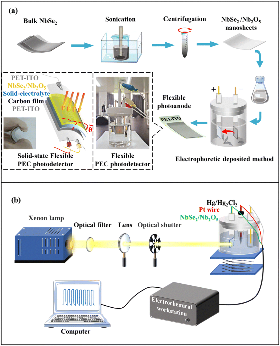 | ||
| Fig. 1 (a) The preparation of the NbSe2/Nb2O5-based PEC photodetector and solid-state PEC photodetector, and (b) photoelectric performance measurement. | ||
The fabricated flexible NbSe2/Nb2O5-based PEC photodetectors were investigated in 1 M Na2SO4 electrolyte. Beyond that, the solid-state PEC photodetector was assembled by NbSe2/Nb2O5 nanosheets, PET-ITO covered with carbon as a counter electrode, and black solid-state electrolyte (Fig. 1a). The real photos of the PEC photodetector and solid-state PEC photodetector can be found in Fig. 1a. These two types of PEC photodetectors were measured based on an electrochemical system, which can work at different power intensities and wavelengths (Fig. 1b). In the PEC-type photodetector, the working electrode is PET-ITO covered with NbSe2/Nb2O5 nanosheets, and the reference electrode is a Hg/Hg2Cl2 electrode while the counter electrode is Pt wire. In contrast, the counter and reference electrodes were both clamped on the same end of PET-ITO while the working electrode was clamped on PET-ITO covered with carbon and 2D NbSe2/Nb2O5 films in the solid-state PEC photodetector.
Results and discussion
Transmission electron microscopy (TEM) was used to verify the successful exfoliation of size-dependent NbSe2 nanosheets from bulk structures under different centrifugation speeds (Fig. 2a–d). The results show that the nanosheet size decreases from 350 to 50 nm in length and from 300 to 25 nm in width. The size and thickness information of the NbSe2 nanosheet under the centrifugation speed of 5000 rpm are also characterized by scanning electron microscopy, as shown in Fig. S1 in the ESI.† The results show that the thickness of the NbSe2/Nb2O5 film is 367.76 nm, which is stacked by nanosheets 113 nm in length and 90 nm in width. The results are in line with the TEM results in Fig. 2.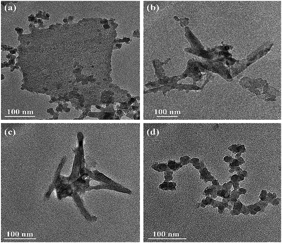 | ||
| Fig. 2 TEM images of NbSe2 nanosheets under the centrifugation speed of (a) 1000 rpm, (b) 3000 rpm, (c) 5000 rpm, and (d) 7000 rpm. | ||
To confirm the size-dependent surface oxidation, atomic force microscopy (AFM) was used, as shown in Fig. 3. The results show that the average thicknesses of the nanosheets under different centrifugation speeds are 133.94, 76.72, 18.78, and 16.49 nm, respectively. In the ultrasonic stripping process, the surface oxide layer with the same thickness was introduced, but the whole thickness of NbSe2/Nb2O5 shows a dramatic difference, thus leading to size-dependent surface oxidation. The results agree well with the XPS results, as shown in Fig. 4.
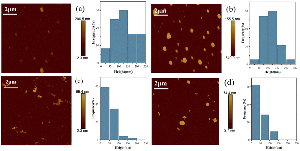 | ||
| Fig. 3 AFM images and statistical size distribution of few-layer NbSe2/Nb2O5 nanosheets under the centrifugation speed of (a) 1000 rpm, (b) 3000 rpm, (c) 5000 rpm, and (d) 7000 rpm. | ||
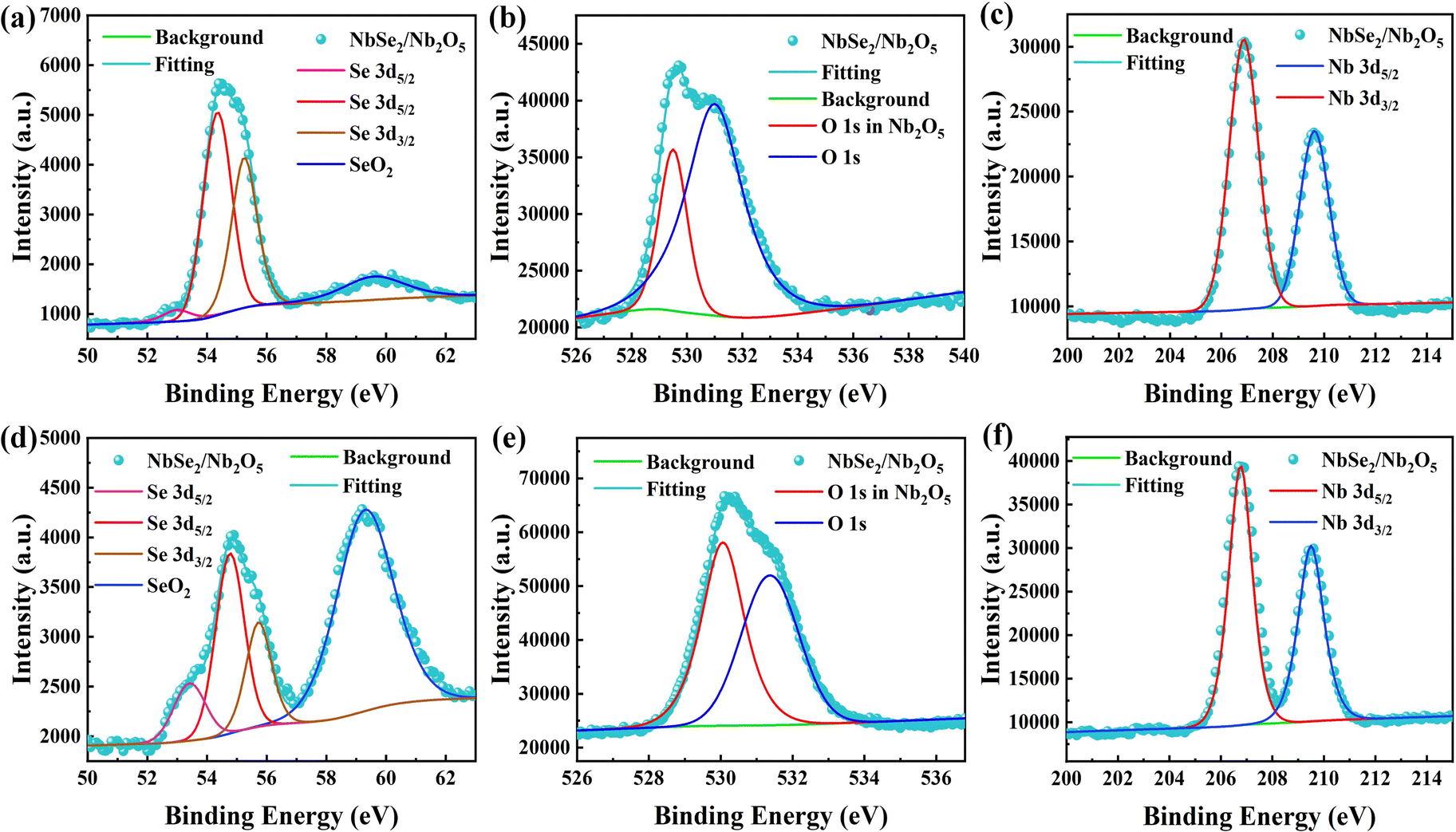 | ||
| Fig. 4 XPS signal of bulk NbSe2 with (a) Se, (b) O, and (c) Nb elements; XPS signal of NbSe2/Nb2O5 nanosheets with (d) Se, (e) O, and (f) Nb elements. | ||
To verify the sample overall composition and crystalline structure, XRD measurements were performed (Fig. S2a) (ESI†). The bulk powder and exfoliated nanosheets of NbSe2 were characterized. Two obvious peaks at 14.26 and 43.49° correspond to (0 0 4) and (0 0 6) planes, indicating the successful preparation of NbSe2 nanosheets.36 However, there is a tiny peak at 9.66° in the exfoliated nanosheets, suggesting a thin surface oxidation (Nb2O5) layer. The thin surface functionalities of NbSe2 are effectively characterized by XPS. The Se 3d spectrum (Fig. 4a) fitted by Se 3d5/2 (53.5 and 54.8 eV) and Se 3d3/2 (55.3 eV) agrees well with NbSe2.37 However, there is a small peak at 59.3 eV from Se 3d, suggesting the presence of selenium oxides. The peaks27 at 531.6 and 530.1 eV (Fig. 4b) belong to O 1s and Nb2O5, respectively. Furthermore, the Nb 3d peaks (Fig. 4c) fitted by Nb 3d5/2 and Nb 3d3/2 locate at 206.9 and 209.5 eV. The peaks correspond to the Nb4+ and Nb5+, indicating the presence of NbSe2 and Nb2O5,28 respectively. The results suggest that the bulk NbSe2 powder has been partly oxidized at the surface. After the NbSe2 nanosheets exfoliated from the bulk powder, the XPS spectra of Se 3d, O 1, and Nb 3d (Fig. 4d–f) were also fitted and these results show the increased amount of Nb2O5. After the formation of the Nb2O5/NbSe2 heterostructure, the binding energy of the O 1s peak has a relative shift towards higher binding energy. These shifts can be explained by the efficient charge transfer from Nb2O5 to Nb2Se5, which is also found in 2D Bi2S3/ReS2,38 SnSe2/SnSe39 and SnS/SnSe240 heterostructures.
Benefiting from the gradient centrifugation method, size-dependent surface oxidation of NbSe2 photoanodes was performed on a flexible PET substrate. The photoelectric properties were firstly investigated under simulated sunlight illumination at 100 mW cm−2 and the I–V curve showed an obvious photovoltaic activity (Fig. S3a) (ESI†). It is known that the photodetectors are sensitive to external bias voltage. To evaluate the photoresponse of the NbSe2/Nb2O5 based PEC-type photodetector under the different centrifugal speeds, time-dependent photocurrent density was measured at 0.2, 0.4, and 0.6 V (Fig. 5a–c), respectively. The steep rise and fall steps demonstrate a fast generation and separation of electron–hole pairs in the different size photodetector devices. Furthermore, all devices show an excellent reproducibility and stability to the on/off state approximately for 10 s per cycle. The photocurrent density (Iph = Ion − Ioff) and responsivity (Rph = Iph/P) parameters are commonly used to assess photodetector performance. The detailed Iph and Rph values of different layers of NbSe2/Nb2O5 photodetectors were measured, as shown in Fig. 5. It is noticeable that the Iph and Rph values of NbSe2/Nb2O5 with different layers all increase with the external bias voltage due to the faster carrier separation under stronger electric fields, as shown in Fig. 5a–c. Among them, especially for the NbSe2/Nb2O5 nanosheet deposited photodetector at 5000 rpm, the Iph values are 0.55, 1.69, 1.46, and 2.32 μA cm−2 and Rph reaches 5.54, 16.95, 14.62, and 23.21 μA W−1 at 0, 0.2, 0.4, and 0.6 V, respectively. Even without external voltage (Fig. S3b) (ESI†), the NbSe2 photodetector still can work due to the built-in electric field at the NbSe2/Nb2O5 interface. These NbSe2/Nb2O5 MSHS-based photodetectors all exhibit more superior photoelectric response in Iph and Rph than those of previously studied BP,41 Te,42 and InSe43 based PEC-type photodetectors (Fig. 5d). This excellent photoelectric response of NbSe2 may origin from the formation of a heterostructure interface between surface oxidation and metallic NbSe2 behavior. The heterostructure prolongs the photoexcited carrier recombination and the metallic behavior of NbSe2 accelerates the charge transfer process. In detail, the carrier separation and transfer pathways at the interface of NbSe2/Nb2O5 are shown in Fig. S4 (ESI†).
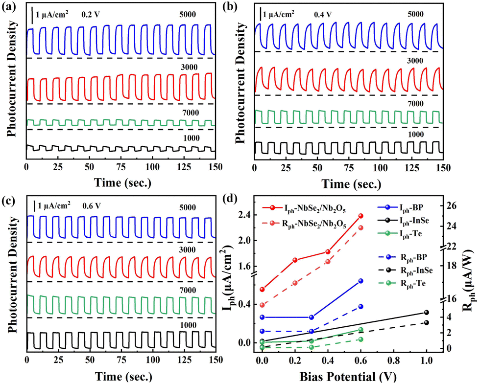 | ||
| Fig. 5 Time-dependent photocurrent density of NbSe2/Nb2O5 under the different centrifugal speed (1000, 3000, 5000, and 7000 rpm)-based PEC photodetectors was measured at (a) 0.2 V, (b) 0.4 V, and (c) 0.6 V; (d) Iph and Rph values of the 2D material-based PEC-type photodetector, including NbSe2/Nb2O5 (this work), BP,41 InSe,43 and Te.42 | ||
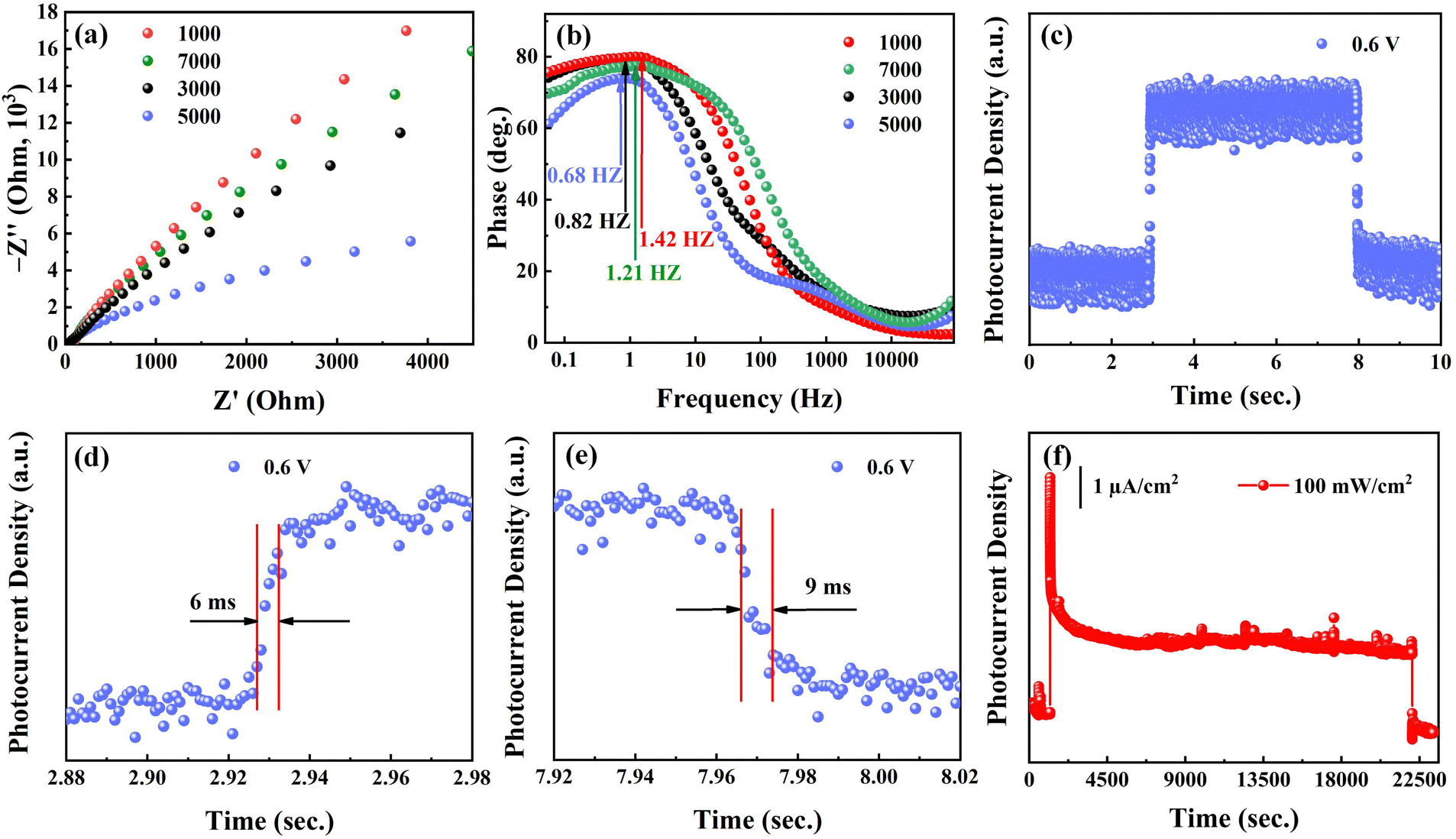
To figure out the performance of the photoelectric response, the carrier transportation efficiency was investigated by electrochemical impedance spectrum (EIS) (Fig. 6a). The smaller semicircle suggests the lower interfacial resistance between the NbSe2/Nb2O5 photoanode and the electrolyte, benefiting carrier separation and transportation. Beyond that, the carrier transportation efficiency can directly reflect from the characteristic peak frequency in Bode phase plots (Fig. 6b). The results demonstrate that the lower frequency of the 5000 rpm nanosheet-coated NbSe2/Nb2O5 film reaches 0.68 Hz, suggesting fast electron transfer. This outstanding carrier separation and recombination property indicates higher response speed. Here, we mainly study the photoelectric performance of the NbSe2/Nb2O5-based photodetector at 5000 rpm. In this work, the response time is characterized by using an optical chopper to generate pulsed light at 1000 Hz (Fig. 6c). From the enlarged rise and fall step (Fig. 6d and e), the rise time (tr) and fall time (tf) are 6 ms and 9 ms at 0.6 V, indicating high sensitivity. The fall time is longer than the rise time, indicating defect states and charge carrier traps in the 2D NbSe2/Nb2O5 materials.44 It is worth pointing out that the response time is 1−2 orders of magnitude faster than previous reported 2D PEC-type photodetectors such as SnS,45 Te,42 InSe,43 Bi2S3,46 and BP41 (Table 1). Despite the lower responsivity in the NbSe2/Nb2O5, such response speed is far superior to FET-type photodetectors such as GeS,47 SnS2,48 and MoS249 due to high electrical conductivity, reduced contact resistance and Schottky barrier.19,20 The high sensitivity promises the NbSe2/Nb2O5 MSHS as a promising alternative for the photodetector, particularly for optical communication and imaging.
 | ||
| Fig. 6 (a) EIS spectra, (b) Bode plots of NbSe2/Nb2O5 photoelectrodes covered with different sizes of nanosheets, (c) response time including (d) rise time (tr) and (e) fall time (tf), and (f) long-term stability measurement. | ||
| Materials | Measurement conditions | Response time | Responsivity | Ref. |
|---|---|---|---|---|
| NbSe2/Nb2O5 | 0.1 M Na2SO4, 0.6 V | 6 ms | 23.84 μA W−1 | This work |
| SnS | 0.1 M Na2SO4, 0.6 V | 0.3 s | 17.8 μA W−1 | 45 |
| Te | 0.1 M Na2SO4, 0.6 V | 70 ms | 1.0–1.3 μA W−1 | 42 |
| InSe | 0.2 M KOH, 1 V | 5 s | 3.3 μA W−1 | 43 |
| Bi2S3 | 0.1 M KOH, 0.6 V | 0.1 s | 52 μA W−1 | 46 |
| BP | 0.1 M KOH, 0 V | 0.5 s | 1.9–2.2 μA W−1 | 41 |
| GeS | FET, 500 nm, Vds = 5 V | 0.85 s | 139.9 μA W−1 | 47 |
| SnS2 | FET, 450 nm, Vds = 10 V | 42 ms | 2 A W−1 | 48 |
| MoS2 | Schottky-contact, Vds = 5 V | 4 s | 880 A W−1 | 49 |
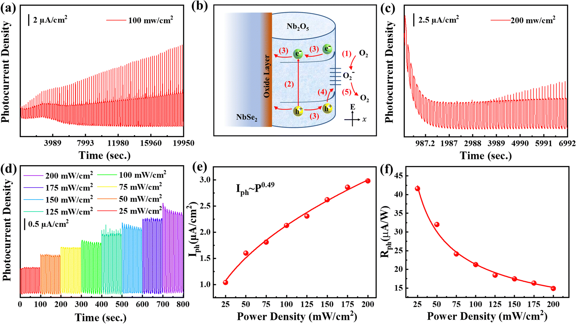
Apart from the sensitivity, the stability of the device is also one of the key performance indicators of commercial photodetectors. The long-term stability tests of the NbSe2/Nb2O5-based photodetector are measured about 23300 s with the applied potential at 0.6 V (Fig. 6f). It can be found that the Iph can still be maintained at a relatively high level (2.10 μA cm−2) even though the photodetector was located in 1 M Na2SO4 electrolyte. However, when we characterize the stability by long cycle measurement under on/off state (Fig. 7a), the Iph gradually increases from 2.0 μA cm−2 to 5.13 μA cm−2 within 19950 s under the same irradiation intensity of 100 mW cm−2. The sharp peak may be from the large amount of electron accumulation and fast recombination. Along with the time variation, the gradually increased Iph may be due to the oxygen-sensitized photoconduction (OSPC) mechanism, which is frequently observed in ZnO,50 WO3,44 and TiO2.51 Furthermore, the surface oxidation has been demonstrated by XPS and this mechanism is mainly dominated by the surface. Based on the OSCP model, there are four main processes (Fig. 7b). (i) Under the dark state, the oxygen molecule is absorbed on the surface of Nb2O5 and acts as an electron capture center [O2(g) + e− → O−2(ad)], thus leading to the surface band bending. (ii) Under the light illumination state, when the photon energy is above the band gap, electron-hole pairs are generated (hv = e− + h+). (iii) Subsequently, the electron-hole pairs are separated by surface band bending and holes flow to the surface while electrons transit from the valence band to the conduction band. (iv) The holes act with the negatively charged oxygen ions, which then release an oxygen molecule [O−2(ad) + h+ → O2(g)]. As the holes are consumed, the unpaired electrons would be captured in the process (i), thus resulting in a longer lifetime and higher photocurrent. Furthermore, the low oxygen content in the electrolyte and lower oxygen adsorption rate would lead to higher Iph with the time variation. After the test is finished, the NbSe2/Nb2O5 was further characterized by XPS (Fig. S5a–c) (ESI†). The results show that the surface oxidation gradually increases, suggesting that the oxygen is consumed and the oxygen adsorption takes place. To verify the oxygen adsorption and desorption process, the oxygen purges electrolyte and promises more oxygen dissolved into the electrolyte. The XPS results (Fig. S5d–f) (ESI†) confirm that the surface NbSe2 has been almost fully oxidized and the oxygen is enough. It is interesting to find that the stable long cycle on/off photocurrent density is approximately 2.98 μA cm−2 even under 200 mW cm−2 (Fig. 7c). These results demonstrated the OSCP takes place due to the surface oxidation.
 | ||
| Fig. 7 (a) Long cycling stability measurement in a low oxygen environment, (b) OSPC mechanism, (c) long cycling stability measurement in enough oxygen environment, (d) light intensity-dependent photocurrent density, and (e) Iph and (f) Rph values extracted from (d). | ||
The surface defects can also be characterized by light intensity photocurrent density, as shown in Fig. 7d. The intensity-dependent Iph and Rph values are extracted (Fig. 7e and f). The Iph curves (Fig. 7e) are fitted by power law (Iph ∼ pθ), and the fitted θ is 0.49 smaller than 1,52,53 indicating the presence of some trap states in the NbSe2 surface. The Rph value (Fig. 7f) decreases with light intensity due to the trap states. Under low light intensity, the photoexcited electrons would be captured by trap states, resulting in reduced recombination.54 Correspondingly, the carrier lifetime is largely prolonged, giving rise to higher Rph. Under high light intensity, the trap states are quickly filled,55 eventually leading to the saturation of Rph.
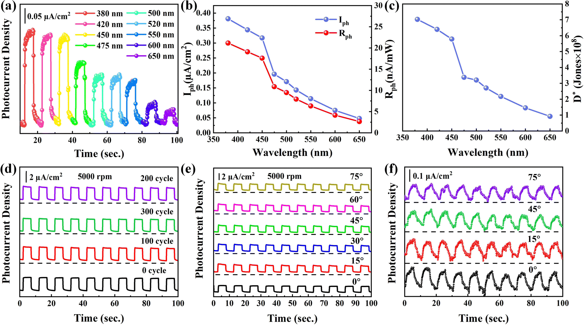
To fully assess the photodetection performance of the NbSe2/Nb2O5 based PEC-type photodetector, the photoelectric response is characterized at the wavelengths of 380, 420, 450, 475, 500, 520, 550, 600, and 650 nm (Fig. 8a). The NbSe2/Nb2O5 shows a higher photoresponsivity at 380 nm, and the value reaches 23.84 μA W−1, which is larger than those of 2D materials such as SnS/SnSe2,40 Te/Se,56 and Nb2C.31 We also extract the Iph and Rph (Fig. 8b) and these values gradually decrease with the wavelength due to the decreased photon absorption as depicted in the UV-Vis spectra (Fig. S2b in ESI†). According to the above-calculated Rph, specific detectivity (D*) is defined and calculated by D* = R × S1/2/(2 × q × Ioff)1/2, where q and S are 1.60 × 10⁻¹⁹ C and 0.6 cm2. The calculated D* value is summarized (Fig. 8c) and the maximum D* value is 7.03 × 10⁸ Jones in 380 nm and the reduced D* with wavelength is due to the high UV response of Nb2O5.26
 | ||
| Fig. 8 (a) Photocurrent density, (b) the calculated Iph and Rph, and (c) specific detectivity (D*) values under different wavelengths; flexibility measurement with (d) different bending cycles and (e) bending angles in the PEC-type photodetector; (f) flexibility measurement in various bending angles in a solid photodetector. | ||
To further test the flexibility performance of the NbSe2/Nb2O5 PEC photodetector, the photoanode was bent approximately at 0, 100, 200, and 300 cycles. The photos of the photodetectors under 0, 100, 200, and 300 cycles can be found in Fig. S6 in the ESI.† The stable photoelectric response is shown in Fig. 8d and the Iph keeps approximately 2.32 μA cm−2, indicating the excellent flexibility performance. Beyond that, the photoresponse was also measured (Fig. 8e) at different bending angles including 0, 15, 45, 60, and 75° and the Iph almost remains the same, which further indicates the NbSe2/Nb2O5 PEC-photodetector with good flexibility. To meet the commercial applications, the solid-state PEC photodetector is greatly anticipated and then the sandwich-structure NbSe2/Nb2O5 photodetector is fabricated, where the aqueous solution is replaced by a solid electrolyte as a charge transfer medium. An obvious on/off photocurrent density signal was observed and the Iph value reaches 0.13 μA cm−2 (Fig. 8f). Even though the solid-state PEC photodetector performance is slightly lower than that of the PEC-type photodetector in the liquid electrolyte, the photocurrent density of the solid device shows no obvious changes even at 15, 45, and 75° after being bent, implying superior flexibility. Compared with the state-of-the-art reports, such as SnS/SnSe2,40 Te/Se,56 and Bi2O2Se/Graphene57 in Table 2, the excellent photodetection performance suggests the further utilization of the NbSe2/Nb2O5 photodetector in highly sensitive, flexible, and wearable optoelectronic devices.
| Materials | Measurement conditions | Response time | Responsivity | Flexible? | Ref. |
|---|---|---|---|---|---|
| NbSe2/Nb2O5 | 0.1 M Na2SO4, 0.6 V | 6 ms | 23.84 μA W−1 | Yes | This work |
| MoS2/WS2 | FET, 405 nm, Vds = 6 V | 9 ms | 298 A W−1 | No | 58 |
| ZnS/MoS2 | ohmic contact, 554 nm, | 11 s | 17.85 μA W−1 | Yes | 59 |
| Graphene/ZnO | Schottky-contact, Vds = 0 V | 32 ms | 50 μA W−1 | No | 60 |
| SnS/SnSe2 | 0.5 M Na2SO4, 0.6 V | 29.6 ms | 4.76 μA W−1 | No | 40 |
| Te/Se | 1.0 M KOH, 0 V | 2 s | 4.04 μA W−1 | No | 41 |
| Bi/Te | 0.5 M KOH, 0 V | 20 ms | 67.67 μA W−1 | No | 61 |
| Bi2O2Se/graphene | KOH/PVA (Quasi-solid) | 0.4 s | 6.5 μA W−1 | Yes | 57 |
| WS2/graphene | H2SO4/PVA (Quasi-solid) | 1.2 s | 36 mA W−1 | Yes | 62 |
Conclusions
In summary, size-dependent NbSe2/Nb2O5 MSHSs were successfully prepared and applied to PEC-type photodetectors. This photodetector shows excellent photodetection performance such as high responsivity (∼23.21 μA W−1), fast response speed at the millisecond level, and broad band detection in the UV-Vis region. It is interesting to find that the Iph is dependent on the ambient environment due to oxygen-sensitized photoconduction. Beyond that, the NbSe2/Nb2O5 MSHS-based PEC-type photodetector still exhibits high photodetection performance and high flexibility even after bending and twisting approximately 300 cycles. The solid-state PEC-type NbSe2/Nb2O5 MSHS photodetector also shows relatively stable photodetection. This work demonstrated that 2D metal-semiconductor heterostructures have great potential in a high-performance optoelectronic device.Author contributions
Xiang Xu: project administration, writing – review and editing & funding acquisition; Chunhui Lu: writing – review and editing, conceptualization; Ying Wang: writing – original draft, formal analysis; Xing Bai: conceptualization & data curation; Zenghui Liu: visualization; Ying Zhang: formal analysis; Dengxin Hua: supervision.Conflicts of interest
The authors declare that they have no known competing financial interests or personal relationships that could have appeared to influence the work reported in this paper.Acknowledgements
This work was supported by the National Natural Science Foundation of China (No. 62105259, 12074311) and the China Postdoctoral Science Foundation (No. 2020M673611XB).Notes and references
- Q. H. Wang, K. Kalantar-Zadeh, A. Kis, J. N. Coleman and M. S. Strano, Nat. Nanotechnol., 2012, 7, 699–712 CrossRef CAS PubMed.
- X. Yu, M. S. Prevot, N. Guijarro and K. Sivula, Nat. Commun., 2015, 6, 7596 CrossRef PubMed.
- K. F. Mak, C. Lee, J. Hone, J. Shan and T. F. Heinz, Phys. Rev. Lett., 2010, 105, 136805 CrossRef PubMed.
- M. Bernardi, M. Palummo and J. C. Grossman, Nano Lett., 2013, 13, 3664–3670 CrossRef CAS PubMed.
- R. Tenne and A. Wold, Appl. Phys. Lett., 1985, 47, 707–709 CrossRef CAS.
- J. Chen, W. Ouyang, W. Yang, J. H. He and X. Fang, Adv. Funct. Mater., 2020, 30 Search PubMed.
- W. Ouyang, F. Teng, J. H. He and X. Fang, Adv. Funct. Mater., 2019, 29 Search PubMed.
- X. Fang, L. Hu, K. Huo, B. Gao, L. Zhao, M. Liao, P. K. Chu, Y. Bando and D. Golberg, Adv. Funct. Mater., 2011, 21, 3907–3915 CrossRef CAS.
- Z. Zhang, Y. Ning and X. Fang, J. Mater. Chem. C, 2019, 7, 223–229 RSC.
- W. Song, J. Chen, Z. Li and X. Fang, Adv. Mater., 2021, 33, 2101059 CrossRef CAS PubMed.
- M. S. El-Bana, D. Wolverson, S. Russo, G. Balakrishnan, D. M. Paul and S. J. Bending, Supercond. Sci. Technol., 2013, 26, 125020 CrossRef.
- J. Li, P. Song, J. Zhao, K. Vaklinova, X. Zhao, Z. Li, Z. Qiu, Z. Wang, L. Lin, M. Zhao, T. S. Herng, Y. Zuo, W. Jonhson, W. Yu, X. Hai, P. Lyu, H. Xu, H. Yang, C. Chen, S. J. Pennycook, J. Ding, J. Teng, A. H. Castro Neto, K. S. Novoselov and J. Lu, Nat. Mater., 2021, 20, 181–187 CrossRef CAS PubMed.
- C. S. Lian, C. Si and W. Duan, Nano Lett., 2018, 18, 2924–2929 CrossRef CAS PubMed.
- S. K. Bae, H. K. Kim, Y. B. Lee, X. F. Xu and S. Iijima, Nat. Nanotechnol., 2011, 5, 574–578 CrossRef PubMed.
- H. G. Shin, H. S. Yoon, J. S. Kim, M. Kim, J. Y. Lim, S. Yu, J. H. Park, Y. Yi, T. Kim and S. C. Jun, Nano Lett., 2018, 18, 1937–1945 CrossRef CAS PubMed.
- R. Corcoran, P. Meeson, Y. Onuki, P. A. Probst and B. L. Gyorffy, J. Phys.: Condens. Matter, 1994, 6, 4479–4492 CrossRef CAS.
- J. Tan, S. Li, B. Liu and H. M. Cheng, Small Struct., 2021, 2, 2000093 CrossRef CAS.
- Y. Zhang, L. Yin, J. Chu, T. A. Shifa, J. Xia, F. Wang, Y. Wen, X. Zhan and H. Jun, Adv. Mater., 2018, 30, 1803665 CrossRef PubMed.
- V. T. Vu, T. Vu, T. L. Phan, W. T. Kang, Y. R. Kim, M. Tran, H. Nguyen, Y. H. Lee and W. J. Yu, ACS Nano, 2021, 15, 13031–13040 CrossRef CAS PubMed.
- D. M. Seo, J. H. Lee, S. Lee, J. Seo and M. G. Hahm, ACS Photonics, 2019, 6, 1379–1386 CrossRef CAS.
- N. Guijarro, M. S. Prevot and K. Sivula, Phys. Chem. Chem. Phys., 2015, 17, 15655–15674 RSC.
- Y.-R. Chang, P.-H. Ho, C.-Y. Wen, T.-P. Chen, S.-S. Li, J.-Y. Wang, M.-K. Li, C.-A. Tsai, R. Sankar, W.-H. Wang, P.-W. Chiu, F.-C. Chou and C.-W. Chen, ACS Photonics, 2017, 4, 2930–2936 CrossRef CAS.
- M. Yamamoto, S. Dutta, S. Aikawa, S. Nakaharai, K. Wakabayashi, M. S. Fuhrer, K. Ueno and K. Tsukagoshi, Nano Lett., 2015, 15, 2067–2073 CrossRef CAS PubMed.
- Y. Wang, A. Chen, S. Lai, X. Peng, S. Zhao, G. Hu, Y. Qiu, J. Ren, X. Liu and J. Luo, J. Catal., 2020, 381, 78–83 CrossRef CAS.
- A. Le Viet, R. Jose, M. V. Reddy, B. V. R. Chowdari and S. Ramakrishna, J. Phys. Chem. C, 2010, 114, 21795–21800 CrossRef CAS.
- R. Ghosh, M. K. Brennaman, T. Uher, M.-R. Ok, E. T. Samulski, L. E. McNeil, T. J. Meyer and R. Lopez, ACS Appl. Mater. Interfaces, 2011, 3, 3929–3935 CrossRef CAS PubMed.
- R. Qu, X. Wen, Y. Zhao, T. Wang, R. Yao and J. Lu, Ultrason. Sonochem., 2021, 73, 105491 CrossRef CAS PubMed.
- H. M. N. Ahmad, S. Ghosh, G. Dutta, A. G. Maddaus, J. G. Tsavalas, S. Hollen and E. Song, J. Phys. Chem. C, 2019, 123, 8671–8680 CrossRef CAS.
- K. Wang, Y. Feng, C. Chang, J. Zhan, C. Wang, Q. Zhao, J. N. Coleman, L. Zhang, W. J. Blau and J. Wang, Nanoscale, 2014, 6, 10530–10535 RSC.
- C. Lu, D. Yang, J. Ma, M. Luo, Y. Jin and X. Xu, Appl. Surf. Sci., 2020, 532, 147409 CrossRef CAS.
- L. Gao, C. Ma, S. Wei, A. V. Kuklin, H. Zhang and H. Agren, ACS Nano, 2021, 15, 954–965 CrossRef CAS PubMed.
- Z. Guo, R. Cao, H. Wang, X. Zhang, F. Meng, X. Chen, S. Gao, D. K. Sang, T. H. Nguyen, A. T. Duong, J. Zhao, Y. J. Zeng, S. Cho, B. Zhao, P. H. Tan, H. Zhang and D. Fan, Natl. Sci. Rev., 2022, 9, nwab098 CrossRef CAS PubMed.
- H. Qiao, Z. Huang, X. Ren, S. Liu, Y. Zhang, X. Qi and H. Zhang, Adv. Opt. Mater., 2019, 8, 1900765 CrossRef.
- T. Fan, Z. Xie, W. Huang, Z. Li and H. Zhang, Nanotechnology, 2019, 30, 114002 CrossRef CAS PubMed.
- Y. Zhang, P. Huang, J. Guo, R. Shi, W. Huang, Z. Shi, L. Wu, F. Zhang, L. Gao, C. Li, X. Zhang, J. Xu and H. Zhang, Adv. Mater., 2020, 32, e2001082 CrossRef PubMed.
- N. D. Boscher, C. J. Carmalt and I. P. Parkin, Eur. J. Inorg. Chem., 2006, 1255–1259 CrossRef CAS.
- H. Wang, X. Huang, J. Lin, J. Cui, Y. Chen, C. Zhu, F. Liu, Q. Zeng, J. Zhou, P. Yu, X. Wang, H. He, S. H. Tsang, W. Gao, K. Suenaga, F. Ma, C. Yang, L. Lu, T. Yu, E. H. T. Teo, G. Liu and Z. Liu, Nat. Commun., 2017, 8, 394 CrossRef PubMed.
- C. Lu, M. Luo, D. Yang, J. Ma, M. Qi and X. Xu, Adv. Mater. Interfaces, 2021, 8, 2100913 CrossRef CAS.
- C. Lu, W. Dong, Y. Zou, Z. Wang, J. Tan, X. Bai, N. Ma, Y. Ge, Q. Zhao and X. Xu, ACS Appl. Mater. Interfaces, 2023, 15, 6156–6168 CrossRef CAS PubMed.
- W. Dong, C. Lu, M. Luo, Y. Liu, T. Han, Y. Ge, X. Xue, Y. Zhou and X. Xu, J. Colloid Interface Sci., 2022, 621, 374–384 CrossRef CAS PubMed.
- X. Ren, Z. Li, Z. Huang, D. Sang, H. Qiao, X. Qi, J. Li, J. Zhong and H. Zhang, Adv. Funct. Mater., 2017, 27, 1606834 CrossRef.
- Z. Xie, C. Xing, W. Huang, T. Fan, Z. Li, J. Zhao, Y. Xiang, Z. Guo, J. Li, Z. Yang, B. Dong, J. Qu, D. Fan and H. Zhang, Adv. Funct. Mater., 2018, 28, 1705833 CrossRef.
- Z. Li, H. Qiao, Z. Guo, X. Ren, Z. Huang, X. Qi, S. C. Dhanabalan, J. S. Ponraj, D. Zhang, J. Li, J. Zhao, J. Zhong and H. Zhang, Adv. Funct. Mater., 2018, 28, 1705237 CrossRef.
- K. Huang, Q. Zhang, F. Yang and D. He, Nano Res., 2010, 3, 281–287 CrossRef CAS.
- W. Huang, Z. Xie, T. Fan, J. Li, Y. Wang, L. Wu, D. Ma, Z. Li, Y. Ge, Z. N. Huang, X. Dai, Y. Xiang, J. Li, X. Zhu and H. Zhang, J. Mater. Chem. C, 2018, 6, 9582–9593 RSC.
- W. Huang, C. Xing and Y. Wang, et al. , Nanoscale, 2018, 10, 2404–2412 RSC.
- C. Y. Lan, C. Li, Y. Yin, H. Y. Guo and S. Wang, J. Mater. Chem. C, 2015, 3, 8074–8079 RSC.
- J. Xia, D. Zhu, L. Wang, B. Huang, X. Huang and X. M. Meng, Adv. Funct. Mater., 2015, 25, 4255–4261 CrossRef CAS.
- O. Lopez-Sanchez, D. Lembke, M. Kayci, A. Radenovic and A. Kis, Nat. Nanotechnol., 2013, 8, 497–501 CrossRef CAS PubMed.
- C. Soci, A. Zhang, B. Xiang, S. A. Dayeh, D. P. R. Aplin, J. Park, X. Y. Bao, Y. H. Lo and D. Wang, Nano Lett., 2007, 7, 1003–1009 CrossRef CAS PubMed.
- R. S. Chen, C. A. Chen, H. Y. Tsai, W. C. Wang and Y. S. Huang, J. Phys. Chem. C, 2012, 116, 4267–4272 CrossRef CAS.
- L. H. Zeng, M. Z. Wang, H. Hu, B. Nie, Y. Q. Yu, C. Y. Wu, L. Wang, J. G. Hu, C. Xie, F. X. Liang and L. B. Luo, ACS Appl. Mater. Interfaces, 2013, 5, 9362–9366 CrossRef CAS PubMed.
- L. Li, E. Auer, M. Liao, X. Fang, T. Zhai, U. K. Gautam, A. Lugstein, Y. Koide, Y. Bando and D. Golberg, Nanoscale, 2011, 3, 1120–1126 RSC.
- L. Wang, J. Jie, Z. Shao, Q. Zhang, X. Zhang, Y. Wang, Z. Sun and S.-T. Lee, Adv. Funct. Mater., 2015, 25, 2910–2919 CrossRef CAS.
- H. Xu, J. Wu, Q. Feng, N. Mao, C. Wang and J. Zhang, Small, 2014, 10, 2300–2306 CrossRef CAS PubMed.
- Y. Wang, F. Zhao, Y. Wang, Y. Zhang, Y. Shen, Y. Feng and W. Feng, Compos. Commun., 2022, 32 Search PubMed.
- G. Chen, Y. Zhou, G. Zhang, J. Li and X. Qi, Ceram. Int., 2021, 47, 25255–25263 CrossRef CAS.
- X. Lin, F. Wang, X. Shan, Y. Miao, X. Chen, M. Yan, L. Zhang, K. Liu, J. Luo and K. Zhang, Appl. Surf. Sci., 2021, 546 CAS.
- P. T. Gomathi, P. Sahatiya and S. Badhulika, Adv. Funct. Mater., 2017, 27 Search PubMed.
- D. Chen, Y. Xin, B. Lu, X. Pan, J. Huang, H. He and Z. Ye, Appl. Surf. Sci., 2020, 529 Search PubMed.
- Y. Zhang, J. Guo, Y. Xu, W. Huang, C. Li, L. Gao, L. Wu, Z. Shi, C. Ma, Y. Ge, X. Zhang and H. Zhang, Nanoscale Horiz., 2020, 5, 847–856 RSC.
- X. Ren, B. Wang, Z. Huang, H. Qiao, C. Duan, Y. Zhou, J. Zhong, Z. Wang and X. Qi, FlatChem, 2021, 25 Search PubMed.
Footnotes |
| † Electronic supplementary information (ESI) available. See DOI: https://doi.org/10.1039/d3nh00172e |
| ‡ Xiang Xu and Chunhui Lu contributed equally to this work. |
| This journal is © The Royal Society of Chemistry 2023 |