
Linear conductance update improvement of CMOS-compatible second-order memristors for fast and energy-efficient training of a neural network using a memristor crossbar array†
See-On
Park
 a,
Taehoon
Park
a,
Hakcheon
Jeong
a,
Seokman
Hong
a,
Seokho
Seo
a,
Yunah
Kwon
b,
Jongwon
Lee
*b and
Shinhyun
Choi
*a
a,
Taehoon
Park
a,
Hakcheon
Jeong
a,
Seokman
Hong
a,
Seokho
Seo
a,
Yunah
Kwon
b,
Jongwon
Lee
*b and
Shinhyun
Choi
*a
aThe School of Electrical Engineering, Korea Advanced Institute of Science and Technology (KAIST), Daejeon 34141, Republic of Korea. E-mail: shinhyun@kaist.ac.kr
bNano Convergence Technology Division, National Nanofab Center (NNFC), 291, Daehak-ro, Daejeon 34141, Republic of Korea. E-mail: temuchin80@nnfc.re.kr
First published on 27th June 2023
Abstract
Memristors are two-terminal memory devices that can change the conductance state and store analog values. Thanks to their simple structure, suitability for high-density integration, and non-volatile characteristics, memristors have been intensively studied as synapses in artificial neural network systems. Memristive synapses in neural networks have theoretically better energy efficiency compared with conventional von Neumann computing processors. However, memristor crossbar array-based neural networks usually suffer from low accuracy because of the non-ideal factors of memristors such as non-linearity and asymmetry, which prevent weights from being programmed to their targeted values. In this article, the improvement in linearity and symmetry of pulse update of a fully CMOS-compatible HfO2-based memristor is discussed, by using a second-order memristor effect with a heating pulse and a voltage divider composed of a series resistor and two diodes. We also demonstrate that the improved device characteristics enable energy-efficient and fast training of a memristor crossbar array-based neural network with high accuracy through a realistic model-based simulation. By improving the memristor device's linearity and symmetry, our results open up the possibility of a trainable memristor crossbar array-based neural network system that possesses great energy efficiency, high area efficiency, and high accuracy at the same time.
New conceptsOur work introduces a novel approach to improve the linear conductance update of memristors, which is crucial for programming a memristor to targeted values and achieving high-performance neuromorphic computing systems. However, memristors usually exhibit non-linear and asymmetry conductance updates. Therefore, many memristor-based systems utilize the ‘non-identical pulse’ which requires extensive peripheral circuitry and long operation time. By exploiting the second-order dynamics of a CMOS-compatible memristor and a simple voltage divider, we achieve significant improvements in memristor linearity without increasing the hardware burden. One of the key differentiators of our work is that we are the first to demonstrate that second-order memristors, which have previously been studied for spike-time-dependent-plasticity learning, can also improve the performance of memristor-based deep neural networks. Our findings provide additional insights into the use of memristors in neuromorphic computing, showing that their material characteristics, such as device temperature via the Joule heating effect, can be leveraged to enhance system performance. In particular, we demonstrate that our proposed method significantly improves the training accuracy of a memristor crossbar array-based neural network for handwritten digit classification, achieving an accuracy of 91.52% compared to 83.64% without our approach. |
Introduction
Artificial neural networks, powered by today's well-matured digital computers, enable several difficult tasks, such as autonomous driving, object detection, and natural language processing, and they have been widely utilized in various industries.1–4 However, conventional von Neumann computing is not desirable for artificial neural networks because it requires data transfer between the memory and processing units.5In a von Neumann computer, the data are stored in a memory unit, but processed in a processing unit that is physically separated from the memory. Usually, training artificial neural networks requires a large amount of training data, commonly called big data; thus, a huge amount of energy is consumed only for data movement.6 In addition, computations in an artificial neural network are composed of simple but massive vector-matrix multiplications. Conventional processing units, such as central processing units (CPUs) and graphics processing units (GPUs), are favored for fast and complex arithmetic calculations, but they can only process data in parallel with a limited number of cores.7 This means that they are not able to process big data in parallel due to the limited number of cores and unnecessary big data movement. Therefore, new computing hardware that can process massive simple vector-matrix multiplications in parallel without data movement between memory and processing units has been extensively studied in the field of artificial neural network hardware.
Memristors, which are two-terminal devices that change their electrical conductance and store analog values, have been widely employed as synapses in artificial neural networks due to their simple structure, non-volatile analog memory properties, and inherent ability to process vector-matrix multiplication when they are fabricated in a crossbar array structure.8–16 Based on the desirable characteristics of the memristor crossbar array, various studies have demonstrated that the energy efficiency, hardware size, and inference speed can be effectively improved compared with the conventional CMOS-based processors12,17,18
Despite the effectiveness of memristors as synapses in neural network systems, it is hard to train the weights of the neural network in a memristor crossbar array. Two-terminal memristors show long retention and fast speed, but they usually undergo severe non-linear and asymmetric update properties.6,8,9,19,20 These prevent a memristor from being programmed to a targeted conductance state because even a single potentiation or depression pulse can induce a catastrophic conductance change (Δw).
To mitigate this non-linearity issue, non-identical pulse methods are usually utilized to program the memristor into the targeted value; for example, applying a short or small amplitude SET (RESET) pulse when the device is fully depressed (potentiated) to suppress abrupt potentiation (depression), and applying a long or high amplitude SET (RESET) pulse when the device is already potentiated (depressed) to enhance the potentiation (depression).21–23 These non-identical pulse methods, called incremental pulse schemes, are effective at programming the device to the targeted value, but they require several peripheral circuits with additional steps and worsen the energy consumption, time consumption, and hardware size of memristor-based neural network systems. For these reasons, it is hard to commercialize memristor-based neural network systems if the energy, time, and area efficiencies are lower than those of conventional CMOS-based neural network systems.
In this study, we fabricated a fully CMOS-compatible HfO2 memristor on an 8-inch wafer and experimentally demonstrated a method to mitigate the severe non-linearity and asymmetry in the memristor. By utilizing a previously reported heating pulse method, we confirmed that the CMOS-compatible HfO2 memristor has a second-order memristor effect and demonstrated that the heating pulse effect largely improves the potentiation linearity of the HfO2 memristor.24 In addition, the depression linearity is also enhanced by connecting a simple passive resistor (voltage divider) serially with the device. The developed method effectively reduces the time and energy consumption for the write and erase processes while improving the update linearity and symmetry. The training accuracy of the memristor crossbar array-based neural network for hand written digit classification is improved from 83.64% to 91.52%, demonstrating that the linearity-improved two-terminal memristor crossbar array can be a good candidate for energy-efficient, compact, and fast neural network systems.
Results and discussion
Fully CMOS-compatible memristor and its non-linearity issues
A fully CMOS-compatible HfO2-based memristor was fabricated, that does not contain any non-CMOS-compatible material such as Au, Pd, or Pt, and does not undergo non-CMOS-compatible fabrication methods (the detailed information for the fabrication is represented in the Experimental section). Fig. 1a and Fig. S1c, d (ESI†) show the metal–insulator–metal structure (TiN/Ti/HfO2/TiN) of the fabricated device on an eight-inch Si wafer. The HfO2 memristor changes its conductance by growing or rupturing an internal conductive filament, which consists of oxygen vacancies (Fig. S2, ESI†).25–27 The oxygen vacancy filament is usually described as a conical or hourglass shape, and several previous studies have revealed that the diameter change of the narrowest part of the filament by removing or inserting oxygen anions induces the device conductance change.27–31 The HfO2 memristor shows reversible resistive switching, with the 100 consecutive I–V sweep results and the 10 consecutive long-term potentiation (LTP) and long-term depression (LTD) curves shown in Fig. S1 (ESI†). The device operates with a fast pulse (<1 μs), and it shows a clear resistance change along with the applied voltage pulses to the top electrode while grounding the bottom electrode, as shown in Fig. 1b. However, severe non-linearity and asymmetry during the LTP–LTD are observed in Fig. 1b, similar to other conventional oxide-based memristors.23,32,33 The device is abruptly potentiated from the high resistance state (HRS) to the low resistance state (LRS) and abruptly depressed from the LRS to the HRS due to abrupt filament growth and rupture, as shown in Fig. 1c. The non-linearity and asymmetry prevent the analog and gradual programming of the device to the targeted value; therefore, the accuracy of the memristor-based neural network is largely degraded. | ||
| Fig. 1 The structure of the fully CMOS-compatible HfO2 memristor and the improvement of the linearity by using the second-order memristor effect and the voltage divider. (a) A cross sectional scanning electron microscopy (SEM) image of the fabricated HfO2 memristor, showing a bottom electrode, TiN/Ti/HfO2/TiN layer, W contact, and pad. (b) LTP–LTD curves of the HfO2 memristor before improvement. 100 consecutive SET pulses (0.7 V, 1 μs) followed by 120 consecutive RESET pulses (−0.8 V, 1 μs) were applied to the device and the conductance state of the device is read by read pulses (0.2 V, 50 μs). Abrupt potentiation and abrupt depression were observed. (c) An illustration of the filament morphology during the potentiation and depression. (d) An illustration of SET pulses with heating pulse (upper) and changes of the state variables in the second-order memristor during the applied SET pulses (lower). (e) A schematic of the memristor with a series resistor for depression linearity improvement. (f) A schematic of the memristor with the voltage divider including two PN diodes and one resistor, preventing the resistor from affecting the potentiation linearity. (g) LTP–LTD curves of the HfO2 memristor with the heating pulse and the voltage divider, showing a highly linear conductance change. 100 consecutive heating and SET pulses (heating pulse: 1 V, 5 μs; SET pulse: 1.35 V, 1 μs) followed by 120 consecutive RESET pulses (−3.6 V, 1 μs) were applied to the device and the conductance state of the device was read by read pulses (0.9 V, 50 μs). Here, larger SET and read voltages were used to compensate the diode turn-on voltage. | ||
Second-order memristors have two state variables to represent the dynamics of the memristors, such as the radius of an oxygen vacancy filament and a device temperature,34–36 compared to conventional first-order memristors having only a single state variable (the radius of the filament), as shown in Fig. S3 (ESI†). Second-order memristors have been actively demonstrated in previous studies, showing that oxide-based memristors can be largely affected not only by the filament radius, but also by the device temperature.34,37
A previous study has demonstrated that potentiation linearity can be improved by introducing a heating pulse to utilize the device temperature as a second variable.24 A heating pulse is a voltage pulse with a small amplitude, that cannot solely change the device's conductance, but is enough to change the device's temperature by the Joule heating effect. This method successfully improves the potentiation linearity, but depression non-linearity, which is usually more severe than potentiation non-linearity, was not discussed.
To improve both the potentiation and the depression linearity at the same time, a heating pulse method is utilized for the potentiation process while a voltage divider is utilized for the depression process, as shown in Fig. 1d and e. In Fig. 1d, the mechanism of the potentiation linearity improvement with the second-order memristor effect is illustrated. The potentiation pulse is composed of two steps, wherein a small heating pulse is followed by a large SET pulse. When the heating pulse is applied, the device's temperature increases and the oxygen anions can be moved more easily with the following SET pulse relative to the case without a heating pulse. This thermal effect is enhanced as the device conductance increases due to Joule heating. Therefore, the potentiation linearity and the dynamic range are largely improved because the thermal effect increases as the device conductance increases, which is similar to non-identical pulse methods that apply a stronger potentiation pulse to the device near the LRS region while applying a weaker potentiation pulse to the device near the HRS region.
On the other hand, the abrupt depression is remedied by the voltage division with the voltage divider circuit, which is composed of a 680 Ω resistor (for this experiment), as shown in Fig. 1e. The resistor is used to divide the applied RESET voltage during the depression process. This makes the effective RESET voltage stronger as the device conductance decreases, which is similar to the non-identical pulse methods applying a stronger RESET voltage as the device conductance is smaller.
Based on the second-order memristor effect and the voltage divider, the conductance update linearity and symmetry are largely improved without sacrificing the conductance on/off ratio, as shown in Fig. 1g. To prevent the voltage divider circuit from deteriorating the potentiation linearity, two PN diodes are added to the voltage divider, which makes the resistor affect only the depression process (Fig. 1f). Both the potentiation and depression processes become linear and symmetric, and the catastrophic potentiation and depression shown in Fig. 1b are mitigated. These improvements cause the memristor to have a rich analog state and enable the accurate programming of the memristor to the targeted value, which is favored for energy-efficient and compact memristor-based neural network systems. Seven consecutive cycles of LTP–LTD curves of the memristor with and without the potentiation or depression linearity improvement are shown in Fig. S4 (ESI†), showing that the improved characteristics with the second-order memristor effect and the voltage divider can be maintained during several cycles.
The second-order memristor effect of the HfO2 memristor for potentiation linearity improvement
HfO2 has very low thermal conductivity compared to other metal oxides such as TiO2 and Al2O3 while showing stable resistive switching characteristics.38 The low thermal conductivity of the switching layer prevents the generated Joule heat from escaping from the switching layer, and therefore, increases the filament temperature. To enhance the thermal effects on the resistive switching of the memristor, the HfO2 deposited by atomic layer deposition (ALD) is selected as a switching layer. The sputtered TiN, which has a much lower thermal conductivity than other metals while having a high electrical conductivity, is utilized as an electrode to increase the thermal effects on the device. To demonstrate the second-order memristive effect in the fabricated fully CMOS-compatible HfO2 memristor controlled by two state variables (filament radius and device temperature), 100 consecutive SET pulses (0.6 V, 1 μs) with different pulse intervals (1, 2, and 5 μs) were applied to the HfO2 memristor (Fig. S5, ESI†). A second-order memristor responds differently to the input frequency because the device temperature increases as the input frequency increases, while a first-order memristor is not affected by the input frequency because it has less temperature dependency. As shown in Fig. S5 (ESI†), the memristor was weakly potentiated during the 100 consecutive SET pulses when the pulse interval was 5 μs. However, when the pulse interval decreased to 2 μs and 1 μs, the potentiation became much stronger as the pulse interval was reduced. The heat generated by Joule heating is removed before the next pulse arrives when the pulse interval is long enough; therefore, the applied electric field is mainly responsible for the oxygen vacancy movement. However, as the pulse interval reduces, the generated heat is not fully removed before the next input pulse arrives, and the oxygen vacancy movement is affected by the heat accumulated in the device (Fig. S5b, ESI†). Because the fabricated HfO2 memristor shows a clear dependency on the input pulse frequency, it is demonstrated that the fabricated memristor has a second-order memristor effect, with filament radius and device temperature as state variables.Based on the second-order memristor effect, the effect of the heating pulse length was analyzed by varying the heating pulse length to observe how the potentiation process changes with the heating pulse length (Fig. 2a and b). The results show that heating pulse lengths longer than 2 μs affect the potentiation, and the dynamic range increases as the heating pulse length increases, demonstrating the effectiveness of the heating pulse for the second-order memristor.
 | ||
| Fig. 2 Effect of the heating pulse on the potentiation process. (a) The potentiation processes with various heating pulse lengths (0.2 V, 0–10 μs) and uniform SET pulse (0.7 V, 1 μs), showing that a heating pulse longer than 2 μs affects the potentiation process due to the Joule heating effect. (b) The applied pulse train form (SET only) for each heating pulse length in (a). (c–e) The heat distribution in the memristor during the heating pulse (c) when the device is in the RESET state, (d) when the device is in the weak SET state, and (e) when the device is in the SET state. | ||
In addition, a multiphysics numerical simulation was conducted to observe how much Joule heat is generated in the HfO2 memristor with different conductance states by modeling the device structure and material properties (Fig. 2c–e).39 To examine the effect of Joule heat for each conductance state of the memristor, simulations have been performed for three different conductance states (RESET, weak SET, and SET states), as shown in Fig. 2c–e. Because the filament is formed by removing oxygen anions from the HfO2 layer, the filament is modeled as non-stoichiometric HfOx.31 In the RESET state, the oxygen anions move to the HfO2 layer from the top electrode, and rupture part of the filament by removing the oxygen vacancy. Therefore, the HfO2 gap is implemented in the filament for simulating the fully RESET state in Fig. 2c. The filament geometry is modeled by referring to previous studies about the filament shape in HfO2-based memristors, which demonstrate the relationship between the filament shape (diameter) and the device conductance.27–31 When a 1 μs, 0.4 V pulse is applied to the HfO2 memristor in the RESET state, a small amount of heat is observed in the filament due to the low current flow through the filament, and the thermal enhancing effect is not dominant. However, when the device is weakly potentiated, as shown in Fig. 2d, a larger Joule heat is observed because of the higher current flow. Finally, when the device is fully potentiated as shown in Fig. 2e, about 800 K of Joule heat is detected in the simulation. The simulation results support the improvement of the potentiation linearity through the heating pulse, as the thermal enhancing effect of the memristor becomes stronger as the device conductance and Joule heat increase, which agrees with the experimental results shown in Fig. 2a.
The optimal range of the heating pulse amplitude and the effects of the HfO2 thickness on the second-order memristor effect are revealed by applying various amplitudes of heating pulses to the fabricated second-order HfO2 memristors with 5, 7.5, and 10 nm of HfO2 thicknesses (Fig. S6, ESI†). The conductance of each device during 100 consecutive set pulses with various heating pulse amplitudes (0 to 0.5 V with 0.1 V interval), followed by 100 consecutive reset pulses. The results show that the heating pulse barely affects the conductance update of a thin (5 nm) HfO2 device, while the heating pulse effect becomes significant as the HfO2 thickness increases. These results demonstrate that the thermal effect is significant for a device with a thicker oxide layer because a thicker oxide layer prevents the generated Joule heat from escaping the device and makes the filament temperature higher than a thinner oxide case. In addition to the effect of the oxide thickness, the optimal range of the heating pulse amplitude is disclosed. As shown in Fig. S6b (ESI†), the larger heating pulse amplitude induces a larger on/off ratio, but the device potentiation linearity becomes significantly degraded when the heating pulse amplitude exceeds 0.5 V. This is because a significantly large heating pulse amplitude (0.5 V) directly makes oxygen anions move to the top electrode and changes the device conductance (Fig. S7, ESI†), as well as generates the Joule heating effect. Therefore, for a significantly large heating pulse amplitude, the device shows a non-linear potentiation curve, and it is confirmed that the heating pulse amplitude must be optimized in a small range (0.1 to 0.4 V).
A voltage divider circuit for depression linearity improvement
Several memristors suffer from the catastrophic depression phenomenon, in which the stored information in the memristor is completely erased by a single RESET pulse.40–43 The fabricated memristor in this study also shows abrupt depression when a single RESET pulse (−0.8 V, 1 μs) is applied to the device in the LRS, as shown in Fig. 3a. If a weaker RESET pulse (−0.6 to −0.75 V, 1 μs) is applied to mitigate catastrophic depression, however, it is impossible to completely reset the memristor to the HRS, which significantly limits the dynamic range of the memristor. Therefore, a weak RESET pulse is favored when the device conductance is high to gradually reduce the device conductance, while a strong RESET pulse is favored when the device conductance is low to fully reset the device to the HRS. | ||
| Fig. 3 Depression linearity improvement through a voltage divider connected to the wire. (a) LTP–LTD curves with 50 consecutive SET pulses (0.7 V, 1 μs) followed by 200 RESET pulses with various amplitudes (−0.6 to −0.8 V, 1 μs). When the amplitude is not high enough, the memristor is not fully depressed, while the catastrophic depression becomes severe when the amplitude is high. (b) The schematic of the memristor and the voltage divider. During the RESET pulse, the applied voltage (Vreset) is divided among the resistor (Vresistor), diode (Vdiode), and memristor (Vmemristor). (c) An illustration representing the effective RESET voltage to the memristor (Vmemristor) being properly adjusted as the memristor conductance (Gmemristor) changes, even though the applied RESET pulses are identical. (d) LTP–LTD curve of the memristor with the voltage divider. Compared with the LTP–LTD curve in (a), it shows highly linear and analog depression characteristics. Here, a SET pulse (1.4 V, 1 μs), RESET pulse (−3.5 V, 1 μs), and read pulse (0.9 V, 50 μs) are used to update and read the device conductance state. | ||
To apply different RESET pulses according to the device's current conductance without the use of additional steps and complex peripheral circuitry, a simple voltage divider composed of a resistor and two PN diodes was connected to the wire of the memristor, as shown in Fig. 3b. When a SET pulse is applied to the memristor, the applied voltage is divided between a PN diode (in parallel with the resistor) and the memristor, while the resistor does not affect the effective voltage across the memristor because the reverse-biased PN diode blocks the potentiation current from flowing through the resistor. However, when the RESET pulse is applied, the applied voltage is divided between the resistor, a PN diode (in series with the resistor), and the memristor. This makes the effective voltage across the memristor increase as the device conductance (resistance) decreases (increases). Therefore, the effective RESET pulse to the memristor is properly adjusted to the device's current conductance state, similar to the RESET pulse of the non-identical pulse method, but without additional steps or peripheral circuitry (Fig. 3c).
The LTP–LTD curve of the HfO2 memristor with a voltage divider is shown in Fig. 3d. Compared with the depression curve without the voltage divider, Fig. 3d shows that the memristor is fully depressed to the HRS by 100 RESET pulses while maintaining good linearity and gradual depression properties. The effect of the series resistor's resistance on the depression linearity is shown in Fig. S8 (ESI†), which demonstrates that the proper selection of the resistor is important for the depression linearity.
It should be noted that adding the voltage divider does not significantly deteriorate the array integration density (Fig. S9, ESI†). In the developed design, one voltage divider is assigned to one row wire, which means that adding the voltage divider does not affect the required area for a single memristor cell. In addition, the area for each voltage divider would be further decreased by substituting the resistor into the transistor. Therefore, considering that the developed method does not require peripheral circuits for the non-identical pulse method, the final array integration density will be smaller compared to the memristor crossbar array utilizing the non-identical pulse method.
Linearity and symmetricity improvements for energy- and time-efficient memristor-based neural network systems
When training a DNN, a weight in the DNN is gradually tuned to the desired value. After the weight is saturated to the specific value, it maintains the value while continuously receiving almost the same number of positive and negative update signals during the training.6 However, when the weight has catastrophic potentiation and depression characteristics, it is difficult for the weight to maintain the desired value even after saturation because a single potentiation or depression signal might completely change the weight value, as shown in Fig. 4a. | ||
| Fig. 4 Linear and analog weight update characteristics without catastrophic potentiation and depression for efficient training of the neural network. (a) An illustration showing the impact of the weight update non-linearity for training neural networks. A single catastrophic change significantly deteriorates the training. (b) Memristor conductance change to the arbitrary SET and RESET pulses. A single depression pulse completely changes the conductance value due to the severe non-linearity. (c) Memristor conductance change to the arbitrary SET and RESET pulses, but with the heating pulse and the voltage divider. It shows linear and gradual potentiation and depression, which enable an efficient training of neural networks. | ||
Fig. 4b shows the response of the HfO2 memristor to arbitrary SET and RESET pulses without the heating pulse and voltage divider. As shown in Fig. 4b, a single SET (RESET) pulse completely potentiates (depresses) the conductance state, and it might deteriorate the accuracy of the neural network, as depicted in Fig. 4a.
On the other hand, Fig. 4c shows the response of the HfO2 memristor to the same input pulse trains as Fig. 4b, but with the heating pulse and the voltage divider present. In this case, arbitrary SET pulses gradually potentiate the conductance with a larger on/off ratio due to the second-order memristor effect. The depression stage after potentiation also shows gradual and linear conductance changes. The gradual and linear potentiation and depression processes enable a reliable artificial neural network based on the memristor crossbar array because catastrophic changes in the weights are eliminated.
The cycle-to-cycle and device-to-device variations before and after utilizing the heating pulse and voltage divider are also analyzed to clarify the impact of the heating pulse and voltage divider on the variations (Fig. S10, ESI†). Through the 10 consecutive LTP–LTD cycles for the HfO2 device with/without the linearity improvements (the heating pulse and voltage divider), the variation coefficients (σ/μ) of LRS and HRS are obtained and demonstrate that the heating pulse and voltage divider have little impact on the cycle-to-cycle variation. Similarly, the LTP–LTD curves are measured from 10 randomly selected devices, and the σ/μ of the LRS and HRS for each case is obtained. As shown in Fig. S10 (ESI†), the device-to-device variation is more significant than the cycle-to-cycle variation in both cases, but the device-to-device variations with/without linearity improvements are similar. The results show that the heating pulse and the voltage divider barely affect the variation of the HfO2 memristor, and therefore, can be utilized for large-scale integration of the memristor array. There have been several approaches to improving the device reliability such as confining the filament,9,11 doping elements in the switching material,44 or optimizing electrode materials,45 and therefore, it is expected that the device reliability can be further improved by adopting those methods. To highlight the advantages of utilizing the second-order memristor effect and the voltage divider compared with the conventional non-identical pulse methods, the required steps to apply a single SET (RESET) pulse for each case are shown in Fig. 5a. For non-identical pulse methods, an extra read operation is first required to check the device's current conductance state. After reading the device's conductance, a proper pulse for the current device conductance must be selected to decide the amplitude or length of the pulse. The read operation and the pulse selecting process, however, consume significant energy and time because an energy-hungry integrator and analog-to-digital converter (ADC) circuits are used for the read operation, and complex peripheral circuits are required for the selecting process.6,18,46 After the read operation and the pulse selecting operation, the peripheral circuit transmits the selected programming pulse to the memristor, and then the SET (RESET) operation is done.
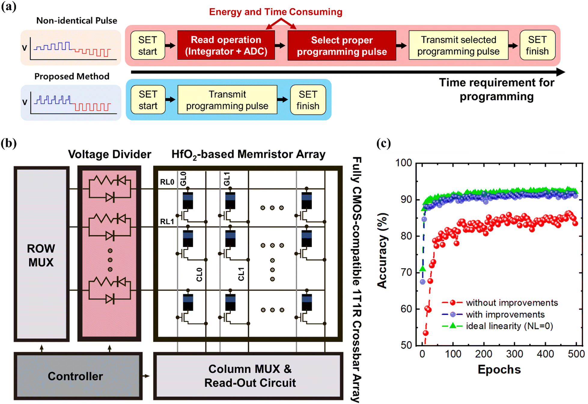 | ||
| Fig. 5 Energy-efficient and fast neural network training with the memristor crossbar array for efficient neural network systems. (a) Comparisons between the non-identical method and the proposed method in this study to improve the linearity. To apply a single SET/RESET pulse, the non-identical pulse method requires two additional steps which consume energy and time, while the proposed method using the second-order memristor effect and the voltage divider does not require any additional steps, and therefore, can be utilized for energy-efficient and fast memristor-based neural network systems. (b) A designed one-transistor-one-memristor (1T1R) crossbar array architecture with the voltage divider connected in the row of the array. The use of the heating pulse and the voltage divider reduces the hardware burden, because the heating pulse can be easily implemented through the ROW MUX circuitry and the voltage divider does not require a large area due to its simplicity. (c) The training accuracy of the 1T1R memristor crossbar array without (red) and with (blue) improvements, and an ideal linearity case (zero non-linearity, green) during 500 epochs of training. | ||
The proposed method in this study, contrary to non-identical pulse methods, does not require any extra steps to SET (RESET) the memristor, and therefore enables energy-efficient and fast SET (RESET) operation. The memristor's conductance update becomes more linear and gradual when the heating pulse and the voltage divider are used; therefore, there is no reason to read the device conductance or select the proper programming pulse before applying it by using energy-hungry read-out circuits and a bulky peripheral circuitry. As a result, the hardware burden to program the memristor is reduced as the voltage divider can be connected to the row or column of the crossbar array and does not require a large area, and the heating pulse can be easily implemented by adding a small voltage pulse before the original SET pulse.
Based on the improved characteristics, a HfO2 memristor-based one-transistor-one-memristor (1T1R) crossbar array was designed and simulated to train a multi-layer perceptron (MLP) network, classifying the hand-written digits in the MNIST data set (Fig. 5b) by using a specialized simulator for memristor MLP.47 To analyze the impact of the linearity improvements on the memristor-based neural network, the LTP–LTD curves of the memristor with and without the proposed method was modeled (Fig. S11, ESI†). The cycle-to-cycle and device-to-device variations with and without the proposed method are also considered in the simulation to clearly assess the impact of the heating pulse and voltage divider for neural network systems. As shown in Fig. 5c, during 500 epochs of training, the memristor-based neural network without the heating pulse and the voltage divider achieves 83.64% training accuracy because severe non-linearity and asymmetry prevent the memristors from being programmed into proper states. On the contrary, the neural network based on the memristor with the heating pulse and voltage dividers successfully trains the weights and achieves 91.52% accuracy, which is close to the training accuracy of the ideal case with zero non-linearity (92.42%), emphasizing the significance of the linearity and symmetry of the memristor for the training of the neural network.
The results demonstrate that the improvement in the linearity and symmetry of the oxide-based memristor can open up the possibility of highly energy-efficient, compact, and time-efficient memristor-based neural network systems that process several massive tasks, including DNNs, by reducing the hardware burden and time to accurately modulate the memristor conductance.
Conclusions
Memristors’ non-linearity and asymmetry during a conductance update make it difficult to accurately tune a memristor to a target value and therefore prevent the development of energy-efficient, compact, and time-efficient memristor-based neural network systems. In this study, a second-order memristor effect and a voltage divider are introduced to improve the linearity and symmetry of a fully CMOS-compatible HfO2 memristor for potentiation and depression. We demonstrate that the fabricated HfO2 memristor is a second-order memristor that possesses filament radius and device temperature as state variables and can be controlled by the device temperature. The potentiation linearity is improved by introducing a heating pulse to utilize the second-order memristor effect, while the depression linearity is improved by connecting a voltage divider circuit composed of a resistor and two diodes to properly adjust the effective RESET voltage. Adding the two improvement methods enables highly linear and analog depression, and eliminates the catastrophic potentiation/depression phenomenon. Finally, hand-written digit classification of the memristor-based MLP using a simulator demonstrates that the linearity and symmetry improvements from the heating pulse and the voltage divider enable the accurate training of a memristor-based neural network. The proposed method to improve device linearity does not require a significant hardware burden; therefore, it provides a way to realize energy-efficient, accurate, and fast training of memristor-based neural network systems.Experimental section
Device fabrication
The fully CMOS-compatible HfO2 memristor is fabricated on the thermally grown 100 nm SiO2 layer with standard CMOS fabrication processes on an 8-inch Si wafer. The bottom electrode metal stack is composed of a TiN/Ti/Al/Ti stack with 150, 10, 450, and 10 nm thickness, respectively. The TiN is selected as a BE material for CMOS compatibility, where a noble metal has been frequently used as a bottom electrode. The 7.5 nm HfO2 layer is grown by ALD, followed by a 10 nm Ti oxygen reservoir layer and TiN top electrode (TE) deposited by a sputtering process. Through X-ray photoelectron spectroscopy (XPS), we demonstrated that the ALD-deposited hafnium oxide has a stoichiometric HfO2 phase, instead of a non-stoichiometric HfOx (Fig. S12, ESI†). The 2 × 2 μm2 active region (TiN/Ti/HfO2) layer is defined by SF6 gas-based inductively coupled plasma-reactive ion etching (ICP-RIE). Finally, an 800 nm SiO2 passivation layer, contact metal lines (W), and the pad (TiN/Ti/Al/Ti) are formed. During the whole fabrication process, any non-CMOS-compatible fabrication or material is not used, which makes it possible to integrate the fabricated memristor on the standard CMOS circuits to build large-scale memristor-based hardware.Memristor-based neural network simulation
To simulate the memristor-based neural network for MNIST classification, NeuroSim V3.0, which is a widely used memristor-based MLP simulator, is utilized to test the effectiveness of the linearity and symmetry improvements in this study.46Based on the experimental data, memristor models before and after the improvements are constructed (Fig. S11, ESI†). The network structure is a three-layer MLP (which means two hidden layers) having a 400 × 100 × 10 structure. The maximum and minimum weights are fixed at 1 and −1, respectively. The device cycle-to-cycle and device-to-device variations before and after improving linearity (without and with the heating pulse and voltage divider) obtained from Fig. S10 (ESI†) are considered for the simulation. To train the weights in the network, the Adam optimizer is used to make the training process faster. Finally, the training accuracy of the memristor-based MLP with and without the improvements, and an ideal linearity case (zero non-linearity) are compared during the 500 epochs of the training.
Author contributions
S. Park and S. Choi: conception of the experiments, methodology, data curation, visualization, and writing original draft. S. Park and T. Park: operation mechanism analysis, S. Park, S. Hong, and S. Seo: software simulation, S. Park and H. Jeong: design 1T1R array and set up the measurement system, Y. Kwon and J. Lee: fabricate the device, J. Lee and S. Choi: supervised the project and writing – review & editing.Conflicts of interest
There are no conflicts to declare.Acknowledgements
This work was supported by the Nanomedical Devices Development Project of NNFC and National R & D Program through the National Research Foundation of Korea (NRF) funded by Ministry of Science and ICT (2022M3I7A2078273 and 2022M3F3A2A01072851).References
- J. Pei, L. Deng, S. Song, M. Zhao, Y. Zhang, S. Wu, G. Wang, Z. Zou, Z. Wu, W. He, F. Chen, N. Deng, S. Wu, Y. Wang, Y. Wu, Z. Yang, C. Ma, G. Li, W. Han, H. Li, H. Wu, R. Zhao, Y. Xie and L. Shi, Towards artificial general intelligence with hybrid Tianjic chip architecture, Nature, 2019, 572, 106–111 CrossRef CAS PubMed.
- K. Roy, A. Jaiswal and P. Panda, Towards spike-based machine intelligence with neuromorphic computing, Nature, 2019, 575, 607–617 CrossRef CAS PubMed.
- D. Ielmini and S. Ambrogio, Emerging neuromorphic devices, Nanotechnology, 2020, 31 CrossRef CAS PubMed.
- S. Hong, H. Choi, J. Park, Y. Bae, K. Kim, W. Lee, S. Lee, H. Lee, S. Cho, J. Ahn, S. Kim, T. Kim, M. Na and S. Cha, Extremely high performance, high density 20nm self-selecting cross-point memory for Compute Express Link, Institute of Electrical and Electronics Engineers (IEEE), 2023, pp. 18.6.1.6.418.6.–.6.418.6.18.6.4.
- Q. Xia and J. J. Yang, Memristive crossbar arrays for brain-inspired computing, Nat. Mater., 2019, 18, 309–323 CrossRef CAS PubMed.
- S. Ambrogio, P. Narayanan, H. Tsai, R. M. Shelby, I. Boybat, C. di Nolfo, S. Sidler, M. Giordano, M. Bodini, N. C. P. Farinha, B. Killeen, C. Cheng, Y. Jaoudi and G. W. Burr, Equivalent-accuracy accelerated neural-network training using analogue memory, Nature, 2018, 558, 60–67 CrossRef CAS PubMed.
- M. A. Zidan, J. P. Strachan and W. D. Lu, The future of electronics based on memristive systems, Nat. Electron., 2018, 1, 22–29 CrossRef.
- S. Srivastava, J. P. Thomas and K. T. Leung, Programmable, electroforming-free TiOx/TaOx heterojunction-based non-volatile memory devices, Nanoscale, 2019, 11, 18159–18168 RSC.
- S. Choi, S. H. Tan, Z. Li, Y. Kim, C. Choi, P. Y. Chen, H. Yeon, S. Yu and J. Kim, SiGe epitaxial memory for neuromorphic computing with reproducible high performance based on engineered dislocations, Nat. Mater., 2018, 17, 335–340 CrossRef CAS PubMed.
- S. Kim, J. Chen, Y. C. Chen, M. H. Kim, H. Kim, M. W. Kwon, S. Hwang, M. Ismail, Y. Li, X. S. Miao, Y. F. Chang and B. G. Park, Neuronal dynamics in HfOx/AlOy-based homeothermic synaptic memristors with low-power and homogeneous resistive switching, Nanoscale, 2019, 11, 237–245 RSC.
- H. Yeon, P. Lin, C. Choi, S. H. Tan, Y. Park, D. Lee, J. Lee, F. Xu, B. Gao, H. Wu, H. Qian, Y. Nie, S. Kim and J. Kim, Alloying conducting channels for reliable neuromorphic computing, Nat. Nanotechnol., 2020, 15, 574–579 CrossRef CAS PubMed.
- P. Yao, H. Wu, B. Gao, J. Tang, Q. Zhang, W. Zhang, J. J. Yang and H. Qian, Fully hardware-implemented memristor convolutional neural network, Nature, 2020, 577, 641–646 CrossRef CAS PubMed.
- F. Kiani, J. Yin, Z. Wang, J. J. Yang and Q. Xia, A fully hardware-based memristive multilayer neural network, Sci. Adv., 2021, 7 Search PubMed.
- H. S. Lee, Y. Baek, Q. Lin, J. Minsu Chen, M. Park, D. Lee, S. Kim and K. Lee, Efficient defect identification via oxide memristive crossbar array based morphological image processing, Adv. Intell. Syst., 2021, 3, 2000202 CrossRef.
- Z. Wang, S. Joshi, S. Savel’Ev, W. Song, R. Midya, Y. Li, M. Rao, P. Yan, S. Asapu, Y. Zhuo, H. Jiang, P. Lin, C. Li, J. H. Yoon, N. K. Upadhyay, J. Zhang, M. Hu, J. P. Strachan, M. Barnell, Q. Wu, H. Wu, R. S. Williams, Q. Xia and J. J. Yang, Fully memristive neural networks for pattern classification with unsupervised learning, Nat. Electron., 2018, 1, 137–145 CrossRef.
- W. Wang, L. Danial, Y. Li, E. Herbelin, E. Pikhay, Y. Roizin, B. Hoffer, Z. Wang and S. Kvatinsky, A memristive deep belief neural network based on silicon synapses, Nat. Electron., 2022, 5, 870–880 CrossRef.
- S. O. Park, H. Jeong, J. Park, J. Bae and S. Choi, Experimental demonstration of highly reliable dynamic memristor for artificial neuron and neuromorphic computing, Nat. Commun., 2022, 13 DOI:10.1038/s41467-022-30539-6.
- F. Cai, J. M. Correll, S. H. Lee, Y. Lim, V. Bothra, Z. Zhang, M. P. Flynn and W. D. Lu, A fully integrated reprogrammable memristor–CMOS system for efficient multiply–accumulate operations, Nat. Electron., 2019, 2, 290–299 CrossRef CAS.
- J. Tang, C. He, J. Tang, K. Yue, Q. Zhang, Y. Liu, Q. Wang, S. Wang, N. Li, C. Shen, Y. Zhao, J. Liu, J. Yuan, Z. Wei, J. Li, K. Watanabe, T. Taniguchi, D. Shang, S. Wang, W. Yang, R. Yang, D. Shi and G. Zhang, A reliable all-2D materials artificial synapse for high energy-efficient neuromorphic computing, Adv. Funct. Mater., 2021, 31 DOI:10.1002/adfm.202011083.
- W. Wu, H. Wu, B. Gao, N. Deng, S. Yu and H. Qian, Improving analog switching in HfOx-based resistive memory with a thermal enhanced layer, IEEE Electron Device Lett., 2017, 38, 1019–1022 CAS.
- H. Liu, M. Wei and Y. Chen, Optimization of non-linear conductance modulation based on metal oxide memristors, Nanotechnol. Rev., 2018, 7, 443–468 CrossRef CAS.
- C. Li, D. Belkin, Y. Li, P. Yan, M. Hu, N. Ge, H. Jiang, E. Montgomery, P. Lin, Z. Wang, W. Song, J. P. Strachan, M. Barnell, Q. Wu, R. S. Williams, J. J. Yang and Q. Xia, Efficient and self-adaptive in-situ learning in multilayer memristor neural networks, Nat. Commun., 2018, 9 DOI:10.1038/s41467-018-04484-2.
- J. H. Ryu and S. Kim, Artificial synaptic characteristics of TiO2/HfO2 memristor with self-rectifying switching for brain-inspired computing, Chaos, Solitons Fractals, 2020, 140 DOI:10.1016/j.chaos.2020.110236.
- Y. J. Jeong, S. Kim and W. D. Lu, Utilizing multiple state variables to improve the dynamic range of analog switching in a memristor, Appl. Phys. Lett., 2015, 107, DOI:10.1063/1.4934818.
- B. Traoré, P. Blaise, E. Vianello, L. Perniola, B. De Salvo and Y. Nishi, HfO2-based RRAM: Electrode effects, Ti/HfO2 interface, charge injection, and oxygen (O) defects diffusion through experiment and ab initio calculations, IEEE Trans. Electron Devices, 2016, 63, 360–368 Search PubMed.
- A. Zeumault, S. Alam, Z. Wood, R. J. Weiss, A. Aziz and G. S. Rose, TCAD modeling of resistive-switching of HfO2 memristors: Efficient device-circuit co-design for neuromorphic systems, Front. Nanotechnol., 2021, 3, DOI:10.3389/fnano.2021.734121.
- A. Fantini, L. Goux, R. Degraeve, D. J. Wouters, N. Raghavan, G. Kar, A. Belmonte, Y.-Y. Chen, B. Govoreanu and M. Jurczak, Intrinsic switching variability in HfO2 RRAM, 2013 IEEE International Memory Workshop (IMW), 2013.
- B. Govoreanu, G. S. Kar, Y.-Y. Chen, V. Paraschiv, S. Kubicek, A. Fantini, I. P. Radu, L. Goux, S. Clima, R. Degraeve, N. Jossart, O. Richard, T. Vandeweyer, K. Seo, P. Hendrickx, G. Pourtois, H. Bender, L. Altimime, D. J. Wouters, J. A. Kittl and M. Jurczak, 10×10nm2 Hf/HfOx crossbar resistive RAM with excellent performance, reliability and low-energy operation, 2011 IEEE International Electron Devices Meeting (IEDM), 2011.
- U. Celano, A. Fantini, R. Degraeve, M. Jurczak, L. Goux and W. Vandervorst, Scalability of valence change memory: From devices to tip-induced filaments, Appl. Phys. Rev., 2016, 6, DOI:10.1063/1.4961150.
- L. Goux, P. Czarnecki, Y. Y. Chen, L. Pantisano, X. P. Wang, R. Degraeve, B. Govoreanu, M. Jurczak, D. J. Wouters and L. Altimime, Evidences of oxygen-mediated resistive-switching mechanism in TiN\HfO2\Pt cells, Appl. Phys. Lett., 2010, 97, DOI:10.1063/1.3527086.
- U. Celano, L. Goux, R. Degraeve, A. Fantini, O. Richard, H. Bender, M. Jurczak and W. Vandervorst, Imaging the three-dimensional conductive channel in filamentary-based oxide resistive switching memory, Nano Lett., 2015, 15, 7970–7975 CrossRef CAS PubMed.
- S. Kim, S. Choi, J. Lee and W. D. Lu, Tuning resistive switching characteristics of tantalum oxide memristors through Si doping, ACS Nano, 2014, 8, 10262–10269 CrossRef CAS PubMed.
- W. Wu, H. Wu, B. Gao, P. Yao, X. Zhang, X. Peng, S. Yu and H. Qian, A Methodology to Improve Linearity of Analog RRAM for Neuromorphic Computing, 2018 IEEE Symposium on VLSI Technology: 18–22, 2018.
- S. Kim, C. Du, P. Sheridan, W. Ma, S. Choi and W. D. Lu, Experimental demonstration of a second-order memristor and its ability to biorealistically implement synaptic plasticity, Nano Lett., 2015, 15, 2203–2211 CrossRef CAS PubMed.
- S. Kumar, X. Wang, J. P. Strachan, Y. Yang and W. D. Lu, Dynamical memristors for higher-complexity neuromorphic computing, Nat. Rev. Mater., 2022, 7, 575–591 CrossRef.
- K. Yang, J. Joshua Yang, R. Huang and Y. Yang, Nonlinearity in memristors for neuromorphic dynamic systems, Small Science, 2022, 2, 2100049 CrossRef CAS.
- A. Rodriguez-Fernandez, C. Cagli, L. Perniola, E. Miranda and J. Suñé, Characterization of HfO2-based devices with indication of second order memristor effects, Microelectron. Eng., 2018, 195, 101–106 CrossRef CAS.
- E. A. Scott, J. T. Gaskins, S. W. King and P. E. Hopkins, Thermal conductivity and thermal boundary resistance of atomic layer deposited high-k dielectric aluminum oxide, hafnium oxide, and titanium oxide thin films on silicon, APL Mater., 2018, 6, DOI:10.1063/1.5021044.
- D. Niraula and V. Karpov, Comprehensive numerical modeling of filamentary RRAM devices including voltage ramp-rate and cycle-to-cycle variations, J. Appl. Phys., 2018, 124, DOI:10.1063/1.5042789.
- N. Ilyas, D. Li, C. Li, X. Jiang, Y. Jiang and W. Li, Analog Switching and Artificial Synaptic Behavior of Ag/SiOx:Ag/TiOx/p++-Si Memristor Device, Nanoscale Res. Lett., 2020, 15, DOI:10.1186/s11671-020-3249-7.
- S. Park, H. Kim, M. Choo, J. Noh, A. Sheri, S. Jung, K. Seo, J. Park, S. Kim, W. Lee, J. Shin, D. Lee, G. Choi, J. Woo, E. Cha, J. Jang, C. Park, M. Jeon, B. Lee, B. H. Lee and H. Hwang, RRAM-based synapse for neuromorphic system with pattern recognition function, in Technical Digest - International Electron Devices Meeting, IEDM, 2012.
- S. Deswal, A. Kumar and A. Kumar, NbOx based memristor as artificial synapse emulating short term plasticity, AIP Adv., 2019, 9, DOI:10.1063/1.5118980.
- M. M. Góis and M. A. Macêdo, Characteristics of analog memristor on thin-film Pt/Co0.2TiO3.2/ITO, J. Mater. Sci.: Mater. Electron., 2020, 31, 5692–5696 CrossRef.
- Y. Y. Chen, R. Roelofs, A. Redolfi, R. Degraeve, D. Crotti, A. Fantini, S. Clima, B. Govoreanu, M. Komura, L. Goux, L. Zhang, A. Belmonte, Q. Xie, J. Maes, G. Pourtois and M. Jurczak, Tailoring switching and endurance/retention reliability characteristics of HfO2/Hf RRAM with Ti, Al, Si dopants, 2014 Symposium on VLSI Technology Digest of Technical Papers, 2014.
- L. Goux, A. Fantini, A. Redolifi, C. Y. Chen, F. F. Shi, R. Degraeve, Y. Y. Chen, T. Witters, G. Groeseneken and M. Jurczak, Role of the Ta scavenger electrode in the excellent switching control and reliability of a scalable low-current operated TiN\Ta2O5\Ta RRAM device, 2014 Symposium on VLSI Technology Digest of Technical Papers, 2014.
- S. Jung, H. Lee, S. Myung, H. Kim, S. K. Yoon, S. W. Kwon, Y. Ju, M. Kim, W. Yi, S. Han, B. Kwon, B. Seo, K. Lee, G. H. Koh, K. Lee, Y. Song, C. Choi, D. Ham and S. J. Kim, A crossbar array of magnetoresistive memory devices for in-memory computing, Nature, 2022, 601, 211–216 CrossRef CAS PubMed.
- Y. Luo, X. Peng and S. Yu, MLP+NeuroSimV3.0: Improving On-chip Learning Performance with Device to Algorithm Optimizations, in ACM International Conference Proceeding Series, Association for Computing Machinery, 2019.
Footnote |
| † Electronic supplementary information (ESI) available. See DOI: https://doi.org/10.1039/d3nh00121k |
| This journal is © The Royal Society of Chemistry 2023 |