
Functionalizing nanophotonic structures with 2D van der Waals materials
Yuan
Meng†
 a,
Hongkun
Zhong†
b,
Zhihao
Xu†
c,
Tiantian
He
b,
Justin S.
Kim
c,
Sangmoon
Han
a,
Sunok
Kim
a,
Seoungwoong
Park
c,
Yijie
Shen
de,
Mali
Gong
b,
Qirong
Xiao
*b and
Sang-Hoon
Bae
*ac
a,
Hongkun
Zhong†
b,
Zhihao
Xu†
c,
Tiantian
He
b,
Justin S.
Kim
c,
Sangmoon
Han
a,
Sunok
Kim
a,
Seoungwoong
Park
c,
Yijie
Shen
de,
Mali
Gong
b,
Qirong
Xiao
*b and
Sang-Hoon
Bae
*ac
aDepartment of Mechanical Engineering and Materials Science, Washington University in St. Louis, St. Louis, MO, USA. E-mail: sbae22@wustl.edu
bState Key Laboratory of Precision Measurement Technology and Instruments, Department of Precision Instrument, Tsinghua University, Beijing, China. E-mail: xiaoqirong@tsinghua.edu.cn
cInstitute of Materials Science and Engineering, Washington University in St. Louis, St. Louis, MO, USA
dDivision of Physics and Applied Physics, School of Physical and Mathematical Sciences, Nanyang Technological University, Singapore, Singapore
eOptoelectronics Research Centre, University of Southampton, Southampton, UK
First published on 8th August 2023
Abstract
The integration of two-dimensional (2D) van der Waals materials with nanostructures has triggered a wide spectrum of optical and optoelectronic applications. Photonic structures of conventional materials typically lack efficient reconfigurability or multifunctionality. Atomically thin 2D materials can thus generate new functionality and reconfigurability for a well-established library of photonic structures such as integrated waveguides, optical fibers, photonic crystals, and metasurfaces, to name a few. Meanwhile, the interaction between light and van der Waals materials can be drastically enhanced as well by leveraging micro-cavities or resonators with high optical confinement. The unique van der Waals surfaces of the 2D materials enable handiness in transfer and mixing with various prefabricated photonic templates with high degrees of freedom, functionalizing as the optical gain, modulation, sensing, or plasmonic media for diverse applications. Here, we review recent advances in synergizing 2D materials to nanophotonic structures for prototyping novel functionality or performance enhancements. Challenges in scalable 2D materials preparations and transfer, as well as emerging opportunities in integrating van der Waals building blocks beyond 2D materials are also discussed.
1. Introduction
The integration of functional materials into photonic structures is essential for building high-performance integrated optoelectronic systems1 and an ideal platform for investigating nanophotonic phenomena.2 The field of photonic integrated circuits3–5 and nanophotonics6,7 has achieved vibrant progress for optical communications,8–10 artificial intelligence,11–13 quantum technology,14,15 imaging,16–18 sensing,19,20 and displays,21–23 to name a few. However, issues such as insufficient multifunctionality and reconfigurability still await further attention. To address these challenges, novel functional materials are required beyond conventional single silicon or a silicon nitride photonics platform24 to generate new functionalities for or impart versatile reconfigurability to the currently established photonic nanostructures.25Two-dimensional (2D) materials are one of such candidates with promising optoelectronic attributes25–28 and have attracted immense research interest over the past decades since the debut of graphene.29 Including graphene,30 transition-metal dichalcogenides (TMDs),31 2D carbides and nitrides (MXenes),32–34 hexagonal boron nitride (h-BN),35 and emergent candidates like quasi-2D halide perovskites,36–43 a big family of 2D materials are established, with a vast collection of available bandgap values.44 As naturally layered materials with interlayer van der Waals interactions, these materials can be exfoliated into atomic monolayers to unveil extraordinary electronic and optoelectronic properties.45
Conventional approaches to impart functional materials rely on heteroepitaxy, which encounters lattice-matching and process compatibility constraints,46 greatly limiting the possible material combos for heterogeneous integration in photonics. When an epilayer and a substrate have different crystal structures or the same crystal structures but with a high lattice parameter distinction, a poly-crystalline phase and defects tend to be generated above certain thickness with compromised material performance.47 In contrast, devoid of the one-to-one chemical bonding between the material layer and the substrate, the 2D materials with signature van der Waals interfaces have made them very easy to transfer, mix, and integrate with other material platforms or prefabricated photonic architectures.48 As prime building blocks for van der Waals integration,48–53 the ultrathin and flexible nature of 2D materials also enable the transfer onto three-dimensional (3D) non-planar optical structures and permit wearable, implantable, and bio-compatible optical applications.54–57
In this review, we outline recent advances in van der Waals materials-enabled nanophotonic applications.50,58,59 We highlight the intriguing outlook on combining 2D van der Waals materials and photonic structures for infusing novel device functionality and reconfigurability to conventional photonic structures and the emergent platform to investigate nanophotonic physics.2,60,61 Fundamental attributes of representative 2D materials and their coupling to exemplary optical structures, such as dielectric waveguides, optical fibers, photonic crystals, and metasurfaces,10,62,63 are cataloged. Furthermore, we also underline recent advents in the van der Waals integration of 3D freestanding nanomembranes. Awaiting challenges and exciting opportunities in this field are also discussed based on current perspectives.
2. Fundamentals for 2D photonics
Nanophotonic structures can be functionalized with diverse 2D materials depending on the base function of the optical architectures and the intrinsic attributes of the 2D materials (Fig. 1).64–67 The valuable fundamental optoelectronic properties and practical considerations on engineering their optical physical coupling are discussed in the following.68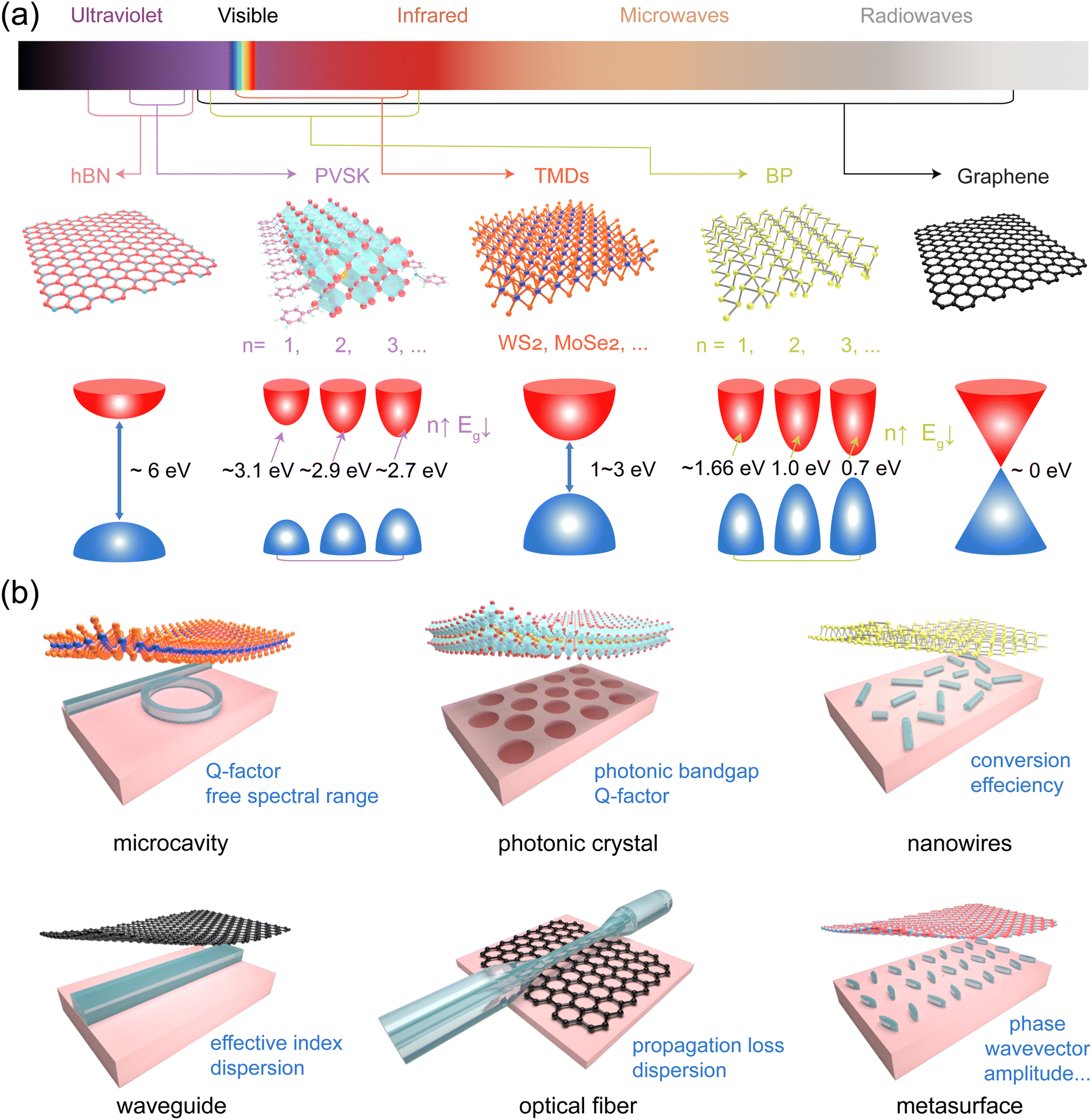 | ||
| Fig. 1 Functionalizing nanophotonic structures with 2D materials. (a) Representative bandgap values of exemplary 2D materials for applications at different wavelengths.44 Beside 2D monolayers, black phosphorus (BP) and quasi-2D perovskites (PVSKs) showcase useful monolayer number (n) dependent bandgaps.114,122 (b) Synergization of various 2D materials with different functional photonic structures. Exemplary physical attributes of the nanophotonic structures are listed in blue color. | ||
2.1. 2D material fundamentals
Frequently applied 2D van der Waals materials in nanophotonics are typically monolayer to few atomic layers in order to reveal extraordinary attributes.27,30 Their outstanding properties along with the atomically clean and electronically keen vdW interfaces to build artificial vdW heterostructures48,69–71 and Moiré superlattices72–75 have rapidly burgeoned as one of the prominent research directions in materials science, photonics, and nanotechnology communities. The complementary metal-oxide semiconductor (CMOS)-compatibility and handiness for transfer have made them candidates for nanophotonic integration (Fig. 1a).76As a monolayer sheet is composed of carbon atoms in a honeycomb-lattice, graphene is a zero-bandgap semimetal with benefits of low density of states,30 high carrier mobility,77 and tunable optical transitions.78 Its unique band structure also enables nonlinear optics79,80 and gate-tunable surface plasmon polaritons (SPPs),81–83 as well as applications for transparent electrodes,84–86 sensors,87 and broadband optical modulation and photodetection.88
In contrast to graphene that lacks an electronic bandgap, 2D semiconductors such as black phosphorus with puckered atomic monolayers exhibit a broadly tunable bandgap from around 0. 3 eV to 2.0 eV depending on layer numbers from the bulk to the monolayer.89,90 For TMD with the general formula of MX2, where “M” represents the transition-metal atom (such as Mo and W), and “X” stands for the chalcogen atom (such as S, Se, or Te),27 their bandgap changes from indirect to direct when exfoliating to monolayers.44 Therefore, these 2D semiconductors are ideal candidates to realize active optical applications, such as light sources, optical amplification, transistors, neuromorphic computing units, and photodetection.91–98 Moreover, a majority of 2D TMDs also possess alluring exitonic and polaritonic physical attributes that are worth studying.74,99–102
h-BN is a wide-bandgap (∼6 eV) 2D material that was originally applied as the optimal substrate for graphene and can be used as insulating or encapsulation layers.35,103 It can provide dangling-bond-free interfaces for photonic van der Waals integration,50 possessing also hyperbolic phonon polaritons,104,105 single-photon emission,106 and second-order nonlinearity.107
Besides conventional 2D materials, 2D MXenes refer to a set of transition metal carbides, carbonitrides and nitrides with layered lattices bound by van der Waals forces as emergent 2D candidates.32,108,109 With the general chemical formula of Mn+1XnTx (n = 1–3; transition metal “M” = Sc, Ti, Zr, Hf, V, Nb, Mo, and so on; “X” = carbon and/or nitrogen and “Tx” is the surface terminations like hydroxyl, oxygen, or fluorine33), they have useful optical applications for saturable absorbers, photodetectors, and modulators.110–112
Metal-halide perovskites are representative organic–inorganic hybrid perovskites that have attracted tremendous research interest over the past decade due to their promising optoelectronic attributes113 for applications in photovoltaics, lasers, LEDs, photodetectors, and nonlinear optics.39,114–121 They typically have corner-sharing BX64− octahedra, where “B” stands for a divalent metal cation like Pb2+, Sn2+ or Ge2+, and “X” denotes a monovalent halide anion.117 Inspired by advents in the 2D materials community, a recent study shows that these materials can also be made into molecularly thin versions like 2D materials.122 With varying dimensions and layer numbers n (Fig. 1a), quasi-2D metal-halide perovskites have different electronic properties, excitonic coupling strength, and varying degrees of quantum-and dielectric-confinement effects for integration with nanophotonic devices.123 For instance, they are good photovoltaic candidates. The presence of organic spacer cations in the material acts as an insulating layer, limiting carrier diffusion between stacked inorganic layers and impeding carrier extraction towards charge transport layers. Consequently, the orientation of layered 2D halide perovskite crystals on a substrate plays a crucial role in determining the overall efficiency of solar cells.117,124,125 Quasi-2D perovskites can also exhibit a notable photoluminescence quantum yield and their photoluminescence emission color can be handily adjusted by modifying the composition or layer number n.38,123 Consequently, 2D halide perovskites possess the capability to generate a broad spectrum of light emissions.126 Moreover, the relatively narrow full width at half maximum of the emission peak contributes to enhanced color purity as a favorable candidate for high-performance LEDs.114
2.2. Photonic structures for coupling with 2D materials
In nanophotonics, judiciously designed optical structures are essential for a vast number of applications.25 For instance, dielectric waveguides are the crucial building blocks in photonic integrated circuits.3 As illustrated in Fig. 1b, when 2D materials are transferred to a photonic waveguide or an optical fiber, they can evanescently couple with the guided electromagnetic modes inside to alter its effective mode index, light propagation, and dispersion.50Optical cavities can spatially confine light into small volumes127,128 to boost light–matter interaction strength for nonlinear,128–131 lasing,132 and sensing applications19,133 when integrated with 2D materials. The synergy of temporal accumulation and spatial confinement of photons can drastically enhance the efficiency of encapsulated 2D materials to the optical resonators.
Photonic crystals are periodic nanostructures with dimension features similar to light wavelength. Under periodic refractive index perturbations, a photonic bandgap emerges.134 They can also be applied as optical cavities for light enhancement and light guiding structures by intentionally introducing point and line defects, respectively.134
In contrast, metasurfaces are engineered optical scatterer arrays with a subwavelength dimension that can achieve powerful control over the fundamental attributes of light,22,95,135–144 such as the phase, wave vector, amplitude, and frequency,145–148 with widespread application such as meta-lenses,149,150 high-efficiency holograms,151,152 color display,21,152–154 ultrathin cloaks,155–157 healthcare sensors,158–162 LiDAR,163–165 functional meta-waveguides,10,166–180 and nonlinear applications,181–183 to name a few.
3. Applications on 2D photonics
Armed with the diverse 2D van der Waals materials building blocks and a large library of photonic structures, massive optical and optoelectronic applications can be prototyped (Fig. 2a–n). Exemplary preparation methods for 2D materials include chemical vapor deposition (CVD), molecular beam epitaxy (MBE), pulsed laser deposition, sputtering, mechanical exfoliation, liquid-phase exfoliation, and so on (Fig. 2o). The recent advents and opportunities are outlined below based on the primal photonic structures coupled with 2D materials.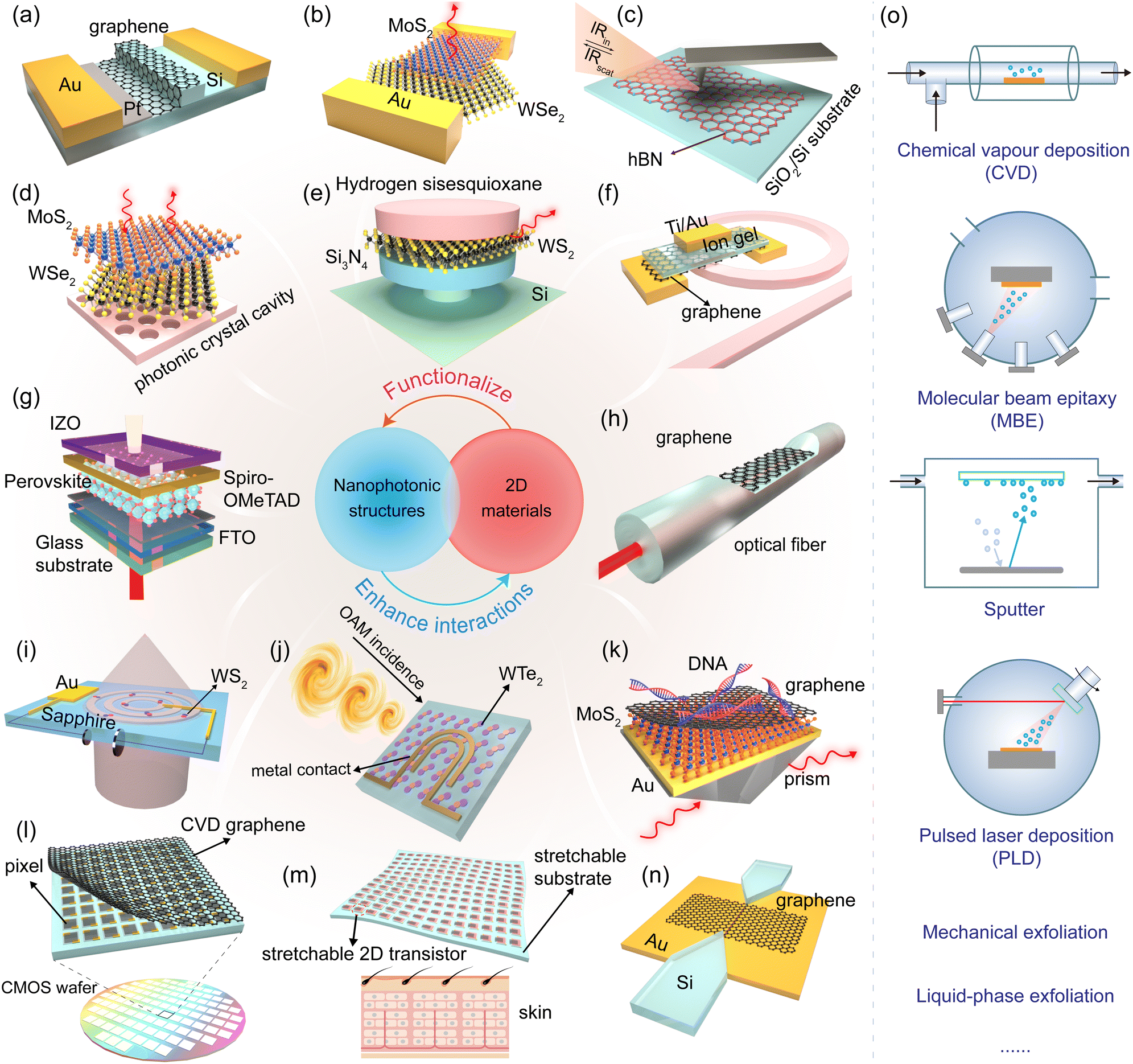 | ||
| Fig. 2 Exemplary 2D-materials-based photonic and optoelectronic applications. (a) Broadband graphene–Si optical modulator.189 (b) Broadband photodetector using the MoS2-WSe2 van der Waals heterostructure.410 (c) Near-field infrared nanoscopy using hBN.411 (d) Nanocavity laser based on monolayer 2D WSe2.219 (e) Excitonic WS2 microdisk nanolaser.221 (f) Gate tunable graphene–SiN frequency comb.236 (g) Perovskite solar cells.10 (h) Broadband graphene polarizer.251 (i) 2D tunable meta-lens.305 (j) OAM detection with WTe2.412 (k) Optical biosensor based graphene–MoS2 layer on a prism.413 (l) Broadband graphene image sensor array.414 (m) Wearable and implantable soft bioelectronics using 2D materials.348 (n) Ultrafast graphene plasmonic all-optical switch.197 (o) Preparation methods for 2D materials. Inspired schematics from ref. 10, 189, 197, 219, 221, 236, 251, 305, 348 and 410–414. | ||
3.1. Optical waveguides
As the essential building block of photonic integrated circuits,3 photonic waveguides are physical structures to guide the propagation of electromagnetic waves.10 By transferring 2D materials such as graphene,26,184 the effective mode index of the underlying dielectric bus waveguide can be controlled via the structure engineering of the waveguide,185 as well as via optical pumping,186 electrical gating,78 strain,187 or thermal tuning188 of the graphene monolayer for optical amplitude189 or phase modulators88,190 (Fig. 2a). The giant optical nonlinearity in graphene and 2D TMD can also be harvested using 2D-laminated waveguide structures for gate-controlled optical nonlinearity.79,191,192 The graphene-integrated waveguides can be leveraged as broadband photodetectors for harvesting guided light signals as well.65,77,91,193,194 For other 2D materials such as TMD and black phosphorus, similar applications are also developed while with different operation wavelengths (Fig. 2b),195,196 and they can be more promising for active optical applications due to the varying bandgap values of these 2D materials.27,44,101Besides, graphene is also an excellent platform to exploit surface plasmon polaritons.82,184 Plasmonic graphene modulators may thus have very compact footprints and fast operation speed albeit higher optical loss (Fig. 2n).197,198 Low-loss surface plasmons can be supported in graphene/h-BN heterostructures with favorable performance in terahertz regions.81,199–202 In contrast, other 2D materials such as TMD are more favorable to exploit nanophotonic polaritons and excitons203,204 and h-BN for phonon polaritons (Fig. 2c). Graphene and other 2D materials can also serve to add reconfigurability to control the coupling169,205 and dispersion206 of the optical waveguides to permit chip-scale optical signal processing. Applications such as plasmonic sensors,207,208 transformation optics,209 nano-imaging,80,210 and gain-modulated lasing applications211,212 can be prototyped as well.
3.2. Micro-cavities
Optical cavities with varying formats are ideal for optical applications that require optical field enhancement and/or strong light–matter interactions.213 Photons can be confined to very small volumes by resonance and recirculation. For instance, Fabry–Perot microcavities fabricated by depositing Bragg reflectors, engineered photonic crystals, and whisper-gallery resonators such as micro-spheres, micro-toroids, and micro-ring resonators with varying quality (Q) factors from thousands to billions.214 The 2D materials such as TMD and black phosphorus can be transferred to or encapsulate into prefabricated optical cavities to harvest strong light enhancement for nano-lasers215–221 (Fig. 2d and e), optical amplification,222 sensing,57,223 and photodetection224,225 to make the most of the atomically thin semiconductor materials with an optical gain.226Another exemplary application direction of 2D materials-coupled optical cavities is nonlinear optics.227 Engineered giant light field enhancement and nonlinear field overlap, the nonlinear optical responses in graphene, TMD, quasi-2D perovskites, black phosphorus, and so on can be boosted in the optical nanocavities228–230 for modulation,231–233 switching,234,235 tunable frequency combs236 (Fig. 2f), and harmonic generation,237,238 and solar-cells (Fig. 2g) to name a few. Alternatively, 2D material nano-sheets can also be directly patterned into nano-resonators by frequency conversion.239
3.3. Optical fibers
As the cornerstone of modern communication system, optical fibers lay the foundation of information communication technology,240 and have been studied for the past few decades with extensions to many fields.241–243 Under the extensive exploration of graphene244 and other 2D materials,31,245 numerous fiber optic devices based on van der Waals materials have been developed throughout the years as a result of their fascinating physical features.64,196,246 Graphene fiber is a typical instance which incorporates graphene to an optical fiber to couple with the propagating light signals inside.247 Compared with the case of integrated dielectric waveguides, 2D materials-coupled optical fibers can have much a longer interaction length between the guided electromagnetic field and 2D materials64,248 for nonlinear harmonic generation,249 sensors,250 mode convertors,240 and imaging.241–243 By harvesting the giant planar anisotropy of graphene, a polarization controller based on graphene has been prototyped that profits from distinct responses upon TE and TM polarized waves by integrating graphene into the side-polished fiber (Fig. 2h),251–253 and microfiber,254–256 as well as other 2D materials sharing similar properties such as BP257–259 and ReS2.260The high carrier mobility261,262 and fast response times263 inside graphene suggest it to be a promising candidate to be used in fabricating high-efficiency photoelectric conversion devices, but graphene is not ideal for an active layer due to the lack of a bandgap and relatively low optical absorption.193,264 Although the absorption performance can be promoted through band structure engineering265 or utilizing the hot electrons generated by the thermo-optic effect,266 another alternative strategy is combining graphene with other optical components267,268 or using TMDs. Monolayer TMD materials can be a competitive choice applied as the active layer interacts directly with outside optical sources.246 Even though having the merits of miniaturized footprints and high conversion efficiency, these 2D materials-based photoelectric conversion devices generally suffer from an obvious drawback of the atomic layer thickness which limits the generation of photocarriers,269 and various strategies have been adopted in order to enhance the light–matter interaction, such as the photoactivation method,270 using heterostructures,271,272 and certain encapsulation.273 A high-performance optical fiber-based modulator is another application direction exploiting various schemes such as thermo-optic,274,275 electro-optic,248,276 and nonlinear effects277,278 based on graphene, BP, TMDs, and so on.279,280 The 2D materials have also been widely used in fiber sensing,250,281 fiber lasers,253,282 and nonlinear optics.248,283
To incorporate 2D materials into optical fibers, two approaches can be applied, namely the transferring-based method and the CVD/direct synthesis-based method.284 Taking graphene as an example, at the early stage of graphene-integrated fibers, the transferring method has been proven a feasible way for transferring graphene layers to the end face of an optical fiber285,286 and the exposed area near the core of tapered277,287 or side-polished fibers.251,288 With the development of graphene growth technology, the CVD method gradually became a promising option featuring mass-production perspectives with high throughput, providing remarkably light–matter interaction albeit require well-controlled fabrication processes.248,249 The possibility of growing other 2D materials on fibers through the CVD method has also been realized in recent pioneering works.289,290
3.4. Metasurfaces
Metasurfaces with artificially engineered optical nanoantennas have showcased unprecedented degrees of freedom in controlling massive fundamental light attributes.135,146 By judiciously altering the material and structure design of the subwavelength nanostructures, the reflected or refracted electromagnetic wave can be flexibly tailored.291–294 As a 2D counter part of metamaterials,295,296 intriguing nanophotonic phenomena and applications can be hatched by combining the 2D nanomaterials.297,298The 2D materials as an ultrathin nano-sheet can be transferred on top of the metasurface to permit electrically or optically reconfigurable or programmable meta-devices (Fig. 2i) for direct polarization or orbital angular momentum detectors (Fig. 2j),299 right routing,61 beam steering,300 lasing,301 and sensing302,303 (Fig. 2k). The metasurface structure can also enable enhanced light-2D material applications for spontaneous control over harmonic signal generation and beam control.137,304 At the same time, the 2D materials can be also patterned into atomically thin metasurfaces for tunable planar optics,305,306 light sources,307,308 beam splitters,309 and so on.
For instance, light possesses multiple attributes, such as intensity, wavelength, polarization, spin, and orbital angular momentum (OAM) for multiplexing and conveying abundant information. However, conventional 2D material photodetectors only detect the light intensity of certain wavelengths which results in a loss of information during the photo-charge conversion process. In contrast, metasurfaces offer an ideal solution to functionalize 2D photodetectors to achieve multi-degree-of-freedom customized direction detection67 on different light properties.137,310–314 For instance, an on-chip polarimeter comprising four metasurface-integrated graphene-silicon photodetectors can detect the full-Stokes parameters, including the intensity, orientation, and ellipticity of arbitrarily polarized incident infrared light.311 Integrated direct OAM detectors can be prototyped as well using 2D TMDs (Fig. 2j).
Besides, incorporating metasurfaces with nonlinear 2D optical materials can enhance design efficiency and convenience. A hybrid structure was proposed to combine the monolayer TMD with the plasmonic metasurface, featuring a chirped metasurface with a gradient-varying groove depth,313 to achieve a coherent SHG signal across the entire visible spectrum.314 A nonlinear synthetic metasurface with the WS2 monolayer was also reported to entangle the phase and spin of light simultaneously as well as manipulate the nonlinear valley-locked chiral emission using 2D WS2 at room temperature.137 Owing to the 2D materials’ diminutive thickness and consequent feeble interaction with light, by integrating the metasurface (typically metal) and graphene into a hybrid structure, the interaction between graphene and light can be greatly enhanced, thereby enabling the in situ control of the optical response from terahertz to infrared wavelengths.314,315 In addition to 2D materials, other low-dimensional materials are also hybridized to metasurfaces for controlled light–matter interactions, lasing, sensing, photocatalysis, polariton physics, and quantum applications.316,317
3.5. Quantum dots and nanowires
Nanostructures such as nanowires (NWs) and quantum dots (QDs) can be optically coupled with 2D material films for active device applications. This coupling is advantageous because these structures can be grown through strain relaxation for high-crystalline structures.318 The unique quantum confinement properties of NWs and QDs allow for precise control over the movement of electrons, making them highly promising for light emitting devices such as LEDs and laser diodes.319 The combination of as-grown NWs and quantum dots (QDs) with transferred 2D or 3D functional nanomembranes offers the possibility of creating novel quantum structures for advanced photodetection and light sources (Fig. 2l).320,321Besides, we can easily spin-coat or transfer NWs (1D) or QDs (0D) onto 2D van der Waals films to achieve 0D/2D or 1D/2D hybrid structures14 to enhance the interaction between light and 2D materials. For instance, metals can function as both photonic components and electrodes to improve the transmittance and external quantum efficiency of the device.322,323 The coupling of nanowires allows for the manipulation of single photon emission and guiding of the emitted photons through the nanowires for quantum emitters.324,325 By combining the Si waveguide and monolayer MoS2, one realized the effective control of directionality, polarization state and spectral emission.326 When coupled with optical fiber NWs, a higher conversion efficiency was achieved on 2D material based second harmonic generation (SHG).269 In addition, optical anisotropy can also be achieved by adjusting the morphology of nanostructures, which allows for the control of resonance frequency and quality factors, using, for instance, 2D material–hybrid plasmonic or optical nanowires.325,327 Moreover, photodetectors can also benefit from 2D materials-coupled QDs with higher responsivity of the 2D films and increased light absorption thanks to the trapping and enhancement of light near the QDs.328
4. Outlook
The synergy between 2D materials and various photonic structures has proven fruitful results in numerous novel optical devices and applications. Exemplary 2D materials and their vdW heterostructure-based photodetectors are compared in Fig. 3a according to their performance indicators.329–332 Graphene, BP, and certain 2D selenides are widely applied to develop broadband devices thanks to their wide-spectrum light absorption or engineerable bandgaps, as indicated with colored horizontal lines. For those operating wavelengths beyond the range of the horizontal axis, gradients are applied, and the maximum wavelength is directly marked out. In contrast, 2D TMDs have proven fruitful results in prototyping photodetectors with high responsivity and fast response times. Representative 3D materials-based photodetectors are also marked out (as open symbols in Fig. 3) for comprehensive comparisons, such as Si, Ge, and group III–V materials,333–336 where they typically are free of the limitations of 2D materials in terms of the limited film thickness towards sufficient light absorption.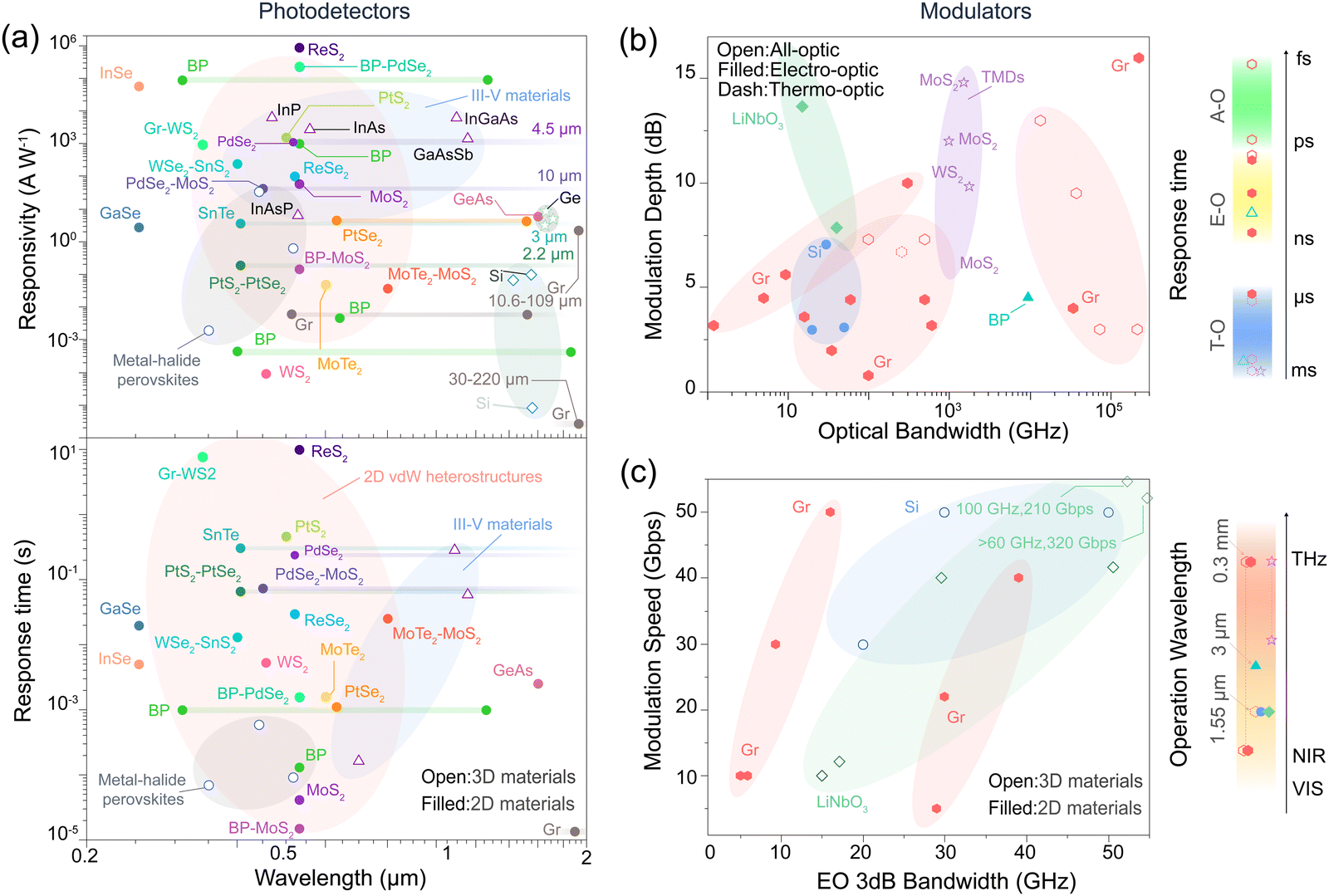 | ||
| Fig. 3 Comparison of exemplary photodetectors and optical modulators based on 2D materials. (a) Scattering plot comparison of responsibility (top) and response time (bottom) versus wavelength for representative 2D materials-based photodetectors (filled symbols). Data are from ref. 329–332. Colored horizontal lines indicate corresponding broadband devices. Exemplary 3D materials-based photodetectors (open symbols) such as Si, Ge, and III–V materials are also marked out for benchmark.333–336 (b) and (c) Scattering plots for optical modulators. (b) Left: comparison of modulation depth and optical operation bandwidth (calculated by |c/λ1 – c/λ2|, c is the light speed and λ1 are λ2 are start and stop operation wavelengths, respectively) for representative 2D materials-based modulators.280,337–342 Right: typical response time of 2D optical modulators with different schemes: all-optical (A-O), electro-optical (E-O), and thermal-optical (T-O). Data from ref. 280, 343 and 344. (c) Left: comparison of silicon-based graphene EO modulators (filled symbols).88,279,345,346 State-of-the-art 3D materials-based optical modulators are also marked out for comparison (open symbols).279,415–418 Right: operation wavelength range of certain 2D optical modulators. Data collected from ref. 280 and 338–342. | ||
Another heavily researched direction is incorporating 2D materials for optical modulation. Typical 2D materials-based optical modulators with different operation schemes are summarized in Fig. 3b, in which the horizontal axis stands for optical operation bandwidth (detailed in figure caption) and the vertical axis stands for modulation depth.280,337–342 To realize high modulation depth (dB μm−1), for instance, the coupling of 2D-laminated optical waveguides needs to be maximized.185 The optical bandwidth, on the other hand, mostly depends on the specific 2D material and device structure (for example, resonance structures like ring resonators, high-Q photonic crystals typically leading to narrowed operation wavelength range).196,279 Different modulation mechanisms also exist. The response time280,343,344 and operation wavelength280,338–342 belonging to different modulation schemes are also drawn respectively in the right panel of Fig. 3b and c. Thermal-based 2D optical modulators typically have a comparatively lower response time with certain thermal cross-talk, while all-optical-based schemes exhibit an ultrafast modulation response time to even femtosecond level.197 Electro-optical (EO) modulators have a fast operation speed between thermal- and all-optical modulators with the highest integration compatibility for photonic integrated circuits,3 which has thus drawn tremendous research interest (mostly implemented as graphene-silicon-based hybrid EO waveguide structures as the left panel of Fig. 3c).88,279,345,346 Emergent 3D materials such as lithium niobate and pure-Si modulators (open symbols) are marked out as well for comparison.
Despite prior vibrant research progress in 2D photonics, several practical challenges still await before enabling new opportunities.
4.1. Challenges
Despite that high-quality 2D material flakes can be produced via mechanical exfoliation,29 they are typically small in size and irregular in shape, and may thus hardly meet the requirements for future industrial practical applications.88,347 In terms of the further commercialization of 2D-materials-based photonic and optoelectronic devices,28 wafer-scale scalable and reproducible 2D material growth and transfer are required.348,349 Liquid-phase exfoliation has a low mass-production cost, but the quality and size of the 2D materials are comparatively low.347Considering the yield and quality, chemical vapor deposition (CVD)-based approaches may permit potentially higher throughput and lower cost compared to mechanical exfoliation or molecular beam epitaxy.350,351 Nevertheless, besides graphene, the direct CVD synthesis of continuous and uniform monolayer 2D materials such as TMD and h-BN is still challenging.350,352–355 To address this trade-off in monolayer controllability and large-scale film uniformity of high-quality 2D materials, the geometrically confined 2D material growth with pre-defined growth pockets can be considered (Fig. 4a).356 The ultimate goal might be the direct synthesis of high-quality 2D monolayers or 2D heterostructures, as a transfer-free method, on top of prefabricated photonic structures.357,358 For the transfer of 2D materials, roll-to-roll scalable transfer359–361 or robot-based precise automatic 2D flake transfer362,363 will be favorable for industrial production.28 Large-scale mechanical exfoliations using nickel348 or atomically flat gold layers364 with the aid of automatic robotic tools are also promising to produce over millimeter-scale 2D films with minimal transfer residue.
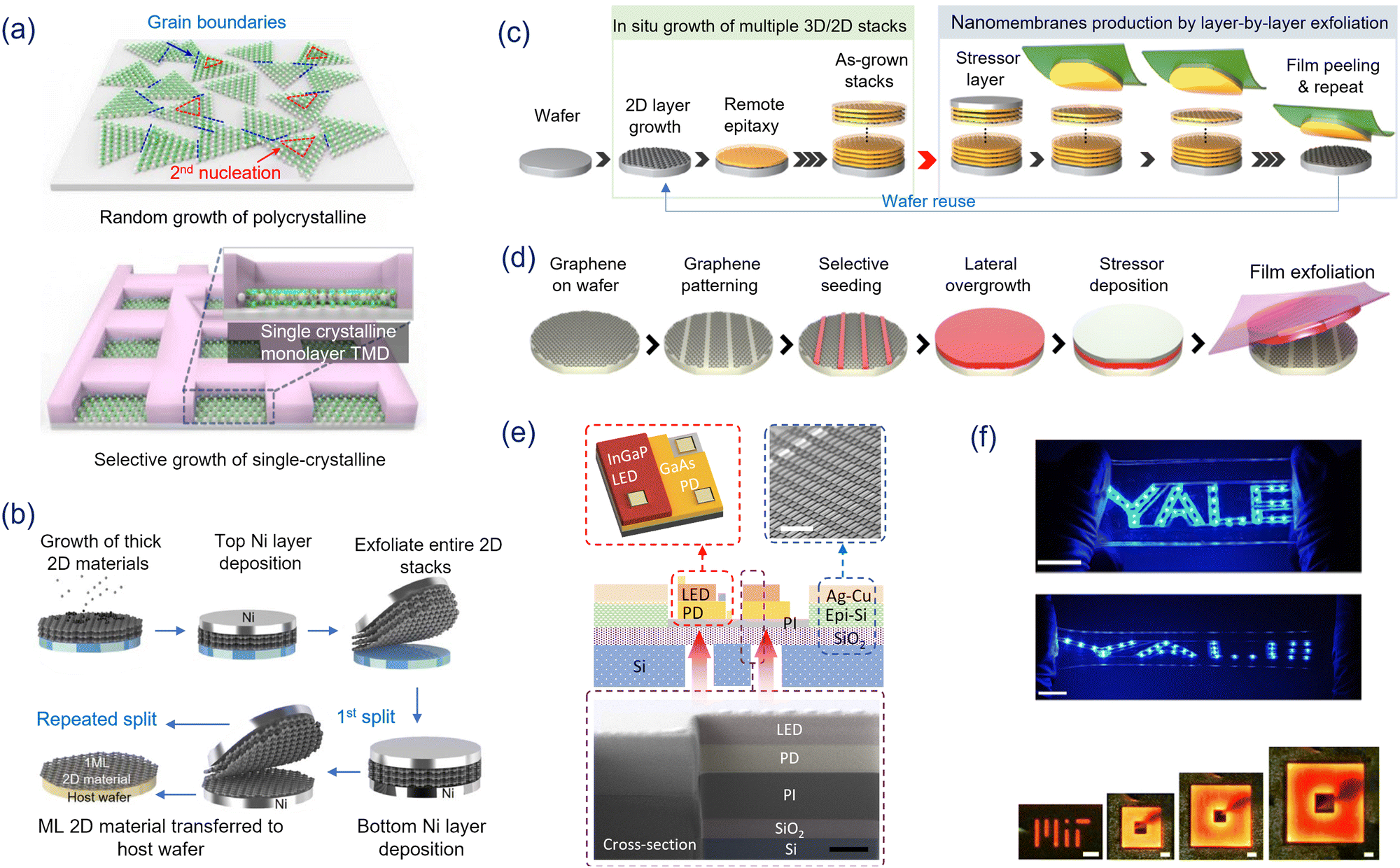 | ||
Fig. 4 Scalable manufacture perspectives of van der Waals materials with exemplary applications. (a) and (b) 2D vdW films. (a) Geometrically confined grown single-crystalline wafer-scale 2D transition metal dichalcogenides (TMD) towards future industrialized 2D photonic integrated circuits.356 (b) Layer-resolved splitting of wafer-scale monolayer (ML) 2D materials.348 (c)–(f) 3D “artificial vdW films”. (c) High-throughput manufacturing of 3D freestanding epitaxial nanomembranes via 2DLT.400 (d) Single-crystalline 3D nanomembranes on graphene nanopatterns for film exfoliation and substrate recycling.387 (b) Reconfigurable hetero-integrated optoelectronic systems with embedded artificial intelligence using vertically stacked optical layers like Lego bricks on a chip.390 (c) Top: stretchable Ga–In thin-film LEDs.395 Bottom: GaAs LEDs made by remote hetroepitaxy on Ge substrates.387 Scale bars: 1 cm (top) and 10![[thin space (1/6-em)]](https://www.rsc.org/images/entities/char_2009.gif) μm (bottom). Panels are adapted with permission from Springer Nature (a,356 c,400 d,387 e390 and f387,395), from AAAS (b348). μm (bottom). Panels are adapted with permission from Springer Nature (a,356 c,400 d,387 e390 and f387,395), from AAAS (b348). | ||
4.2. Perspectives
Recently, several emerging 2D materials with exotic attributes have provided further opportunities,38,117,122 such as 2D van der Waals materials with vanished interlayer coupling for scalable nonlinear optical applications,365 quasi-2D perovskites with high crystallinity,37,40,122 and ferroelectricity and ferromagnetism in atomically thin van der Waals layered materials.366–369 Due to their quantum confinement of charge carriers and excitons and tunable bandgap, quasi-2D halide perovskites have excellent optoelectronic properties for light sources, photovoltaics, and photodetectors.122,370 The limited stability of conventional 3D halide perovskites has posed a significant challenge to their commercialization. Employing quasi-2D perovskites can be a substitute for their 3D bulk counterparts, where the metal-halide octahedra are better shielded against moisture and oxygen due to the presence of hydrophobic organic ligands. These organic ligands can also contribute to reducing the distortion of the metal-halide octahedra and preventing phase transitions by means of steric hindrance with comparatively suppressed anionic migration as well.Confined growth-enabled large-scale integrated photonic devices356 are also promising for future industrialized 2D integrated photonic circuits (Fig. 4a).10,357 The layer resolved splitting technique that engineers the stressor level difference of the top and bottom metal layers (typically nickel) can also be applied to produce wafer-scale big 2D monolayers from bulk 2D stacks (Fig. 4b).348
Besides, 2D materials that have a minuscule thickness limit their interaction length with electromagnetic waves,50 and recent advances on remote epitaxy371–373 and van der Waals epitaxy374–376 also permit various three-dimensional (3D) freestanding nanomembranes (Fig. 4c),50,375,377–380 as well as other 3D layer exfoliation techniques by epitaxial chemical lift-off, mechanical exfoliation or laser lift-off.68,381–386 These thin films are also made ultrathin with artificially defined van der Waals interfaces for photonic van der Waals integration,48,50,120 on graphene-covered templates for defect-reduced heteroepitaxy (Fig. 4d) with potential to re-use the costly wafers towards film manufacture cost reduction.387 These 3D nanomembranes can preserve their optical attributes almost independent from film thickness68,386 for versatile light-emitting,388 sensing,389 smart embedded optoelectronic processors (Fig. 4e),390 light enhancement,391,392 new integrated photonics platforms,393 solar cells,394 flexible LEDs (Fig. 4f),387,395 and other novel hetero-integrated devices.68,396,397 Nanomembrane mass production could also be enabled with a reduced cost.387,398–400
By combining the 2D and 3D van der Waals material building blocks, vast playgrounds also unfold for 2D-materials-based photonic integrated circuits3,4,25,66,279 (Fig. 5a), exotic nanophotonic polaritons in hybrid heterostructures2,58,59 (Fig. 5b), flexible, wearable and implantable optoelectronic biosensors20,54,158,207 (Fig. 5c), and vertical 3D integrated circuits and systems390,401–403 (Fig. 5d). Stacked 2D vdW heterostructures with a certain precise twist angle have enabled exciting electronic attributes from the interference of Moiré superlattices.72,75,404 The deterministic stacking of hybrid 2D and 3D vdW materials405 or nanophotonic structures406–409 may hatch intriguing twist-induced photonic and polaritonic physics as well.74
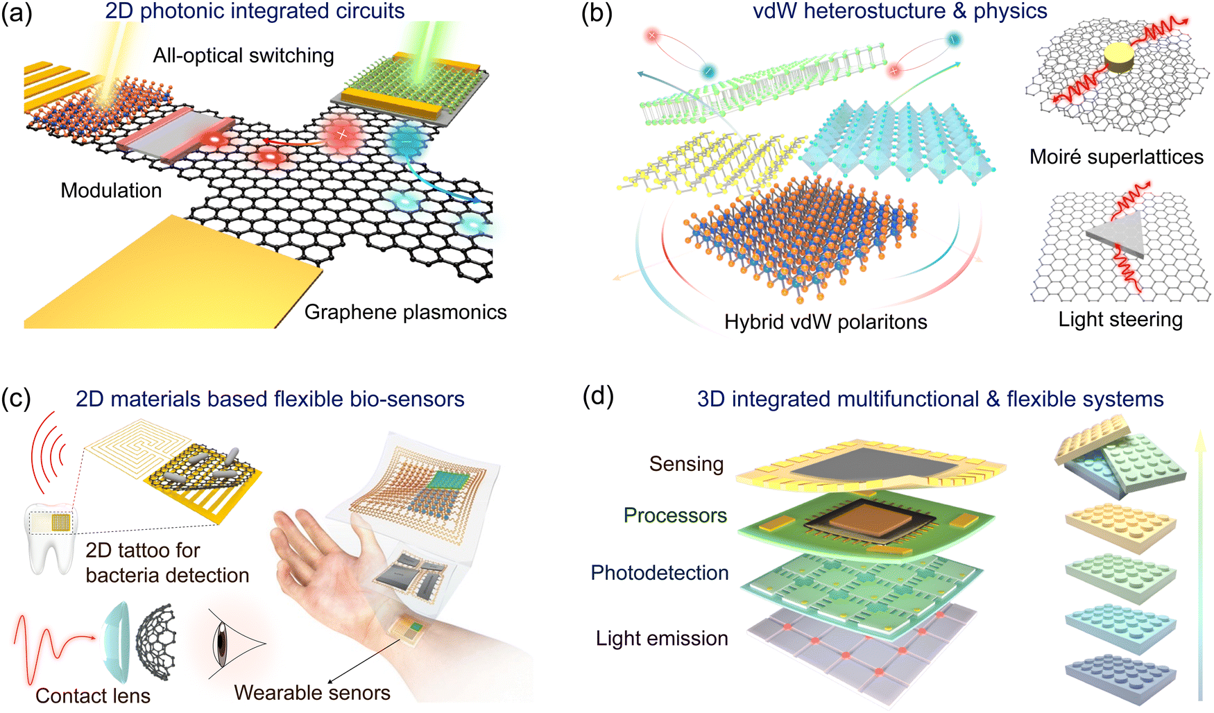 | ||
| Fig. 5 Outlook on 2D van der Waals photonics. (a) On-chip integrated photonic and plasmonic circuits based on 2D van der Waals (vdW) materials.2 (b) Novel polaritonic physics and light manipulation based on 2D and hybrid vdW heterostructures.2,50 (c) Wearable and implantable optoelectronic biosensors.419–421 (d) Stackable optoelectronic chip circuity for scalable and multifunctional nano-systems.390 Panel (a) and the right panel of (b) are adapted from ref. 2 (Springer Nature) with permission. Panel (c) right is adapted with permission from ref. 419 (Wiley). The left panels of (c) are inspired from ref. 420 and 421. Panel (d) is inspired from ref. 50 (Springer Nature). | ||
Author contributions
All authors have reviewed and approved the final version of the manuscript. Conceptualization: Y. M., S.-H. B., and Q. X.; investigation: Y. M., H. Z., Z. X., S. H., S. K., S. P., Y. S., and M. G.; visualization: H. Z. and Y. M.; writing – original draft: Y. M., H. Z., Z. X., T. H., and J. S. K; writing – review and editing: Y. M., Q. X., and S.-H. B.; supervision: S.-H. B. and Q. X.; and project administration: S.-H. B.Conflicts of interest
The authors declare no conflicts of interest.Acknowledgements
Q. X. thanks support of the National Natural Science Foundation of China (62075113 and 62122040).References
- M. Tran, et al., Extending the spectrum of fully integrated photonics, Nature, 2022, 610, 54–60 CrossRef PubMed.
- Q. Zhang, et al., Interface nano-optics with van der Waals polaritons, Nature, 2021, 597, 187–195 CrossRef PubMed.
- D. Marpaung, J. Yao and J. Capmany, Integrated microwave photonics, Nat. Photonics, 2019, 13, 80–90 CrossRef CAS.
- H. Shu, et al., Microcomb-driven silicon photonic systems, Nature, 2022, 605, 457–463, DOI:10.1038/s41586-022-04579-3.
- D. T. Spencer, et al., An optical-frequency synthesizer using integrated photonics, Nature, 2018, 557, 81–85, DOI:10.1038/s41586-018-0065-7.
- P. Chao, B. Strekha, R. Kuate Defo, S. Molesky and A. W. Rodriguez, Physical limits in electromagnetism, Nat. Rev. Phys., 2022, 4, 543–559, DOI:10.1038/s42254-022-00468-w.
- Y. Yang, et al., A general theoretical and experimental framework for nanoscale electromagnetism, Nature, 2019, 576, 248–252, DOI:10.1038/s41586-019-1803-1.
- C. Sun, et al., Single-chip microprocessor that communicates directly using light, Nature, 2015, 528, 534–538, DOI:10.1038/nature16454.
- A. H. Atabaki, et al., Integrating photonics with silicon nanoelectronics for the next generation of systems on a chip, Nature, 2018, 556, 349–354, DOI:10.1038/s41586-018-0028-z.
- Y. Meng, et al., Optical meta-waveguides for integrated photonics and beyond, Light Sci. Appl., 2021, 10, 235, DOI:10.1038/s41377-021-00655-x.
- Y. Shen, et al., Deep learning with coherent nanophotonic circuits, Nat. Photonics, 2017, 11, 441–446, DOI:10.1038/nphoton.2017.93.
- X. Wang, P. Xie, B. Chen and X. Zhang, Chip-Based High-Dimensional Optical Neural Network, Nano-Micro Lett., 2022, 14, 221, DOI:10.1007/s40820-022-00957-8.
- W. Bogaerts, et al., Programmable photonic circuits, Nature, 2020, 586, 207–216 CrossRef CAS PubMed.
- A. W. Elshaari, W. Pernice, K. Srinivasan, O. Benson and V. Zwiller, Hybrid integrated quantum photonic circuits, Nat. Photonics, 2020, 14, 285–298 CrossRef CAS PubMed.
- J. Wang, F. Sciarrino, A. Laing and M. G. Thompson, Integrated photonic quantum technologies, Nat. Photonics, 2020, 14, 273–284, DOI:10.1038/s41566-019-0532-1.
- C. Rogers, et al., A universal 3D imaging sensor on a silicon photonics platform, Nature, 2021, 590, 256–261, DOI:10.1038/s41586-021-03259-y.
- X. Zhang, K. Kwon, J. Henriksson, J. Luo and M. C. Wu, A large-scale microelectromechanical-systems-based silicon photonics LiDAR, Nature, 2022, 603, 253–258, DOI:10.1038/s41586-022-04415-8.
- J. Wu, et al., An integrated imaging sensor for aberration-corrected 3D photography, Nature, 2022, 612, 62–71, DOI:10.1038/s41586-022-05306-8.
- W. Chen, Ş. Kaya Özdemir, G. Zhao, J. Wiersig and L. Yang, Exceptional points enhance sensing in an optical microcavity, Nature, 2017, 548, 192–196, DOI:10.1038/nature23281.
- H. Altug, S.-H. Oh, S. A. Maier and J. Homola, Advances and applications of nanophotonic biosensors, Nat. Nanotechnol., 2022, 17, 5–16, DOI:10.1038/s41565-021-01045-5.
- H. Wang, et al., Coloured vortex beams with incoherent white light illumination, Nat. Nanotechnol., 2023, 18, 264–272, DOI:10.1038/s41565-023-01319-0.
- Z. Shen, et al., Monocular metasurface camera for passive single-shot 4D imaging, Nat. Commun., 2023, 14, 1035, DOI:10.1038/s41467-023-36812-6.
- C. He, Y. Shen and A. Forbes, Towards higher-dimensional structured light, Light Sci. Appl, 2022, 11, 205, DOI:10.1038/s41377-022-00897-3.
- D. J. Moss, R. Morandotti, A. L. Gaeta and M. Lipson, New CMOS-compatible platforms based on silicon nitride and Hydex for nonlinear optics, Nat. Photonics, 2013, 7, 597–607, DOI:10.1038/nphoton.2013.183.
- F. Xia, H. Wang, D. Xiao, M. Dubey and A. Ramasubramaniam, Two-dimensional material nanophotonics, Nat. Photonics, 2014, 8, 899–907, DOI:10.1038/nphoton.2014.271.
- F. Bonaccorso, Z. Sun, T. Hasan and A. C. Ferrari, Graphene photonics and optoelectronics, Nat. Photonics, 2010, 4, 611–622, DOI:10.1038/nphoton.2010.186.
- S. Manzeli, D. Ovchinnikov, D. Pasquier, O. V. Yazyev and A. Kis, 2D transition metal dichalcogenides, Nat. Rev. Mater., 2017, 2, 1–15 Search PubMed.
- W. Kong, et al., Path towards graphene commercialization from lab to market, Nat. Nanotechnol., 2019, 14, 927–938, DOI:10.1038/s41565-019-0555-2.
- A. K. Geim and K. S. Novoselov, The rise of graphene, Nat. Mater., 2007, 6, 183–191 CrossRef CAS PubMed.
- A. C. Neto, F. Guinea, N. M. Peres, K. S. Novoselov and A. K. Geim, The electronic properties of graphene, Rev. Mod. Phys., 2009, 81, 109 CrossRef.
- Q. H. Wang, K. Kalantar-Zadeh, A. Kis, J. N. Coleman and M. S. Strano, Electronics and optoelectronics of two-dimensional transition metal dichalcogenides, Nat. Nanotechnol., 2012, 7, 699–712 CrossRef CAS PubMed.
- Y. Wang, Y. Xu, M. Hu, H. Ling and X. J. N. Zhu, MXenes: Focus on optical and electronic properties and corresponding applications, Nanophotonics, 2020, 9, 1601–1620 CrossRef CAS.
- B. Anasori, M. R. Lukatskaya and Y. J. N. R. M. Gogotsi, 2D metal carbides and nitrides (MXenes) for energy storage, Nat. Rev. Mater., 2017, 2, 1–17 Search PubMed.
- T. Zhao,
et al., Ultrathin MXene assemblies approach the intrinsic absorption limit in the 0.5–10THz band, Nat. Photonics, 2023, 17, 622–628, DOI:10.1038/s41566-023-01197-x.
- J. D. Caldwell, et al., Photonics with hexagonal boron nitride, Nat. Rev. Mater., 2019, 4, 552–567 CrossRef CAS.
- L. Dou, et al., Atomically thin two-dimensional organic-inorganic hybrid perovskites, Science, 2015, 349, 1518–1521 CrossRef CAS PubMed.
- D. Ji, et al., Freestanding crystalline oxide perovskites down to the monolayer limit, Nature, 2019, 570, 87–90, DOI:10.1038/s41586-019-1255-7.
- A. G. Ricciardulli, S. Yang, J. H. Smet and M. Saliba, Emerging perovskite monolayers, Nat. Mater., 2021, 20, 1325–1336 CrossRef CAS PubMed.
- J. Feng, et al., Single-crystalline layered metal-halide perovskite nanowires for ultrasensitive photodetectors, Nat. Electron., 2018, 1, 404–410 CrossRef CAS.
- J. Feng, et al., Crystallographically Aligned Perovskite Structures for High-Performance Polarization-Sensitive Photodetectors, Adv. Mater., 2017, 29, 1605993, DOI:10.1002/adma.201605993.
- Y. Zhao, et al., Suppressing ion migration in metal halide perovskite via interstitial doping with a trace amount of multivalent cations, Nat. Mater., 2022, 21, 1396–1402, DOI:10.1038/s41563-022-01390-3.
- Y. Zhao, et al., Molecular Interaction Regulates the Performance and Longevity of Defect Passivation for Metal Halide Perovskite Solar Cells, J. Am. Chem. Soc., 2020, 142, 20071–20079, DOI:10.1021/jacs.0c09560.
- Y. Chen, et al., Compact spin-valley-locked perovskite emission, Nat. Mater., 2023 DOI:10.1038/s41563-023-01531-2.
- A. Chaves, et al., Bandgap engineering of two-dimensional semiconductor materials, npj 2D Mater. Appl., 2020, 4, 29, DOI:10.1038/s41699-020-00162-4.
- A. K. Geim and I. V. Grigorieva, van der Waals heterostructures, Nature, 2013, 499, 419–425 CrossRef CAS PubMed.
- Y. Hu, et al., III/V-on-Si MQW lasers by using a novel photonic integration method of regrowth on a bonding template, Light Sci. Appl., 2019, 8, 93, DOI:10.1038/s41377-019-0202-6.
- A. Castellanos-Gomez, et al., van der Waals heterostructures, Nat. Rev. Methods Primers, 2022, 2, 58 CrossRef CAS.
- Y. Liu, Y. Huang and X. Duan, van der Waals integration before and beyond two-dimensional materials, Nature, 2019, 567, 323–333, DOI:10.1038/s41586-019-1013-x.
- C.-h Liu, J. Zheng, Y. Chen, T. Fryett and A. Majumdar, van der Waals materials integrated nanophotonic devices [Invited, Opt. Mater. Express, 2019, 9, 384–399, DOI:10.1364/OME.9.000384.
- Y. Meng, et al., Photonic van der Waals integration from 2D materials to 3D nanomembranes, Nat. Rev. Mater., 2023, 8, 498–517, DOI:10.1038/s41578-023-00558-w.
- H. Wang, et al., van der Waals Integration Based on Two-Dimensional Materials for High-Performance Infrared Photodetectors, Adv. Funct. Mater., 2021, 31, 2103106, DOI:10.1002/adfm.202103106.
- N. Flöry, et al., Waveguide-integrated van der Waals heterostructure photodetector at telecom wavelengths with high speed and high responsivity, Nat. Nanotechnol., 2020, 15, 118–124, DOI:10.1038/s41565-019-0602-z.
- H. Ling, R. Li and A. R. Davoyan, All van der Waals Integrated Nanophotonics with Bulk Transition Metal Dichalcogenides, ACS Photonics, 2021, 8, 721–730, DOI:10.1021/acsphotonics.0c01964.
- S.-H. Oh, et al., Nanophotonic biosensors harnessing van der Waals materials, Nat. Commun., 2021, 12, 1–18 CrossRef PubMed.
- Y. Qiao, et al., Graphene-based wearable sensors, Nanoscale, 2019, 11, 18923–18945, 10.1039/C9NR05532K.
- S.-H. Bae, et al., Graphene-based transparent strain sensor, Carbon, 2013, 51, 236–242, DOI:10.1016/j.carbon.2012.08.048.
- H.-L. Hou, C. Anichini, P. Samorì, A. Criado and M. Prato, 2D van der Waals Heterostructures for Chemical Sensing, Adv. Funct. Mater., 2022, 32, 2207065, DOI:10.1002/adfm.202207065.
- Z. Dai, et al., Artificial metaphotonics born naturally in two dimensions, Chem. Rev., 2020, 120, 6197–6246 CrossRef CAS PubMed.
- H. Lin, et al., Engineering van der Waals materials for advanced metaphotonics, Chem. Rev., 2022, 122, 15204–15355 CrossRef CAS PubMed.
- S.-H. Bae, et al., Unveiling the carrier transport mechanism in epitaxial graphene for forming wafer-scale, single-domain graphene, Proc. Natl. Acad. Sci. U. S. A., 2017, 114, 4082–4086, DOI:10.1073/pnas.1620176114.
- Y. Chen, et al., Chirality-dependent unidirectional routing of WS2 valley photons in a nanocircuit, Nat. Nanotechnol., 2022, 17, 1178–1182, DOI:10.1038/s41565-022-01217-x.
- J. Kim, et al., Scalable manufacturing of high-index atomic layer–polymer hybrid metasurfaces for metaphotonics in the visible, Nat. Mater., 2023, 22, 474–481, DOI:10.1038/s41563-023-01485-5.
- Y. Yang, et al., Revisiting Optical Material Platforms for Efficient Linear and Nonlinear Dielectric Metasurfaces in the Ultraviolet, Visible, and Infrared, ACS Photonics, 2023, 10, 307–321, DOI:10.1021/acsphotonics.2c01341.
- J.-h Chen, Y.-f Xiong, F. Xu and Y.-q Lu, Silica optical fiber integrated with two-dimensional materials: towards opto-electro-mechanical technology, Light Sci. Appl., 2021, 10, 78, DOI:10.1038/s41377-021-00520-x.
- Z. Sun and H. Chang, Graphene and Graphene-like Two-Dimensional Materials in Photodetection: Mechanisms and Methodology, ACS Nano, 2014, 8, 4133–4156, DOI:10.1021/nn500508c.
- X. Wang, et al., Recent Advances in the Functional 2D Photonic and Optoelectronic Devices, Adv. Opt. Mater., 2019, 7, 1801274, DOI:10.1002/adom.201801274.
- A. Elbanna, et al., 2D Material Infrared Photonics and Plasmonics, ACS Nano, 2023, 17, 4134–4179, DOI:10.1021/acsnano.2c10705.
- S.-H. Bae, et al., Integration of bulk materials with two-dimensional materials for physical coupling and applications, Nat. Mater., 2019, 18, 550–560, DOI:10.1038/s41563-019-0335-2.
- Y. Liu, et al., van der Waals heterostructures and devices, Nat. Rev. Mater., 2016, 1, 1–17 Search PubMed.
- P. V. Pham, et al., 2D Heterostructures for Ubiquitous Electronics and Optoelectronics: Principles, Opportunities, and Challenges, Chem. Rev., 2022, 122, 6514–6613, DOI:10.1021/acs.chemrev.1c00735.
- H. H. Yoon, et al., Miniaturized spectrometers with a tunable van der Waals junction, Science, 2022, 378, 296–299, DOI:10.1126/science.add8544.
- Y. Cao, et al., Unconventional superconductivity in magic-angle graphene superlattices, Nature, 2018, 556, 43–50 CrossRef CAS PubMed.
- E. C. Regan, et al., Mott and generalized Wigner crystal states in WSe2/WS2 moiré superlattices, Nature, 2020, 579, 359–363 CrossRef CAS PubMed.
- D. Huang, J. Choi, C.-K. Shih and X. Li, Excitons in semiconductor moiré superlattices, Nat. Nanotechnol., 2022, 17, 227–238 CrossRef CAS PubMed.
- F. He, et al., Moiré Patterns in 2D Materials: A Review, ACS Nano, 2021, 15, 5944–5958, DOI:10.1021/acsnano.0c10435.
- Y. Wu, et al., Manipulating polaritons at the extreme scale in van der Waals materials, Nat. Rev. Phys., 2022, 4, 578–594, DOI:10.1038/s42254-022-00472-0.
- F. Xia, T. Mueller, Y.-M. Lin, A. Valdes-Garcia and P. Avouris, Ultrafast graphene photodetector, Nat. Nanotechnol., 2009, 4, 839–843, DOI:10.1038/nnano.2009.292.
- F. Wang, et al., Gate-variable optical transitions in graphene, Science, 2008, 320, 206–209 CrossRef CAS PubMed.
- T. Jiang, et al., Gate-tunable third-order nonlinear optical response of massless Dirac fermions in graphene, Nat. Photonics, 2018, 12, 430–436 CrossRef CAS.
- T. Jiang, V. Kravtsov, M. Tokman, A. Belyanin and M. B. Raschke, Ultrafast coherent nonlinear nanooptics and nanoimaging of graphene, Nat. Nanotechnol., 2019, 14, 838–843 CrossRef CAS PubMed.
- A. Woessner, et al., Highly confined low-loss plasmons in graphene–boron nitride heterostructures, Nat. Mater., 2015, 14, 421–425 CrossRef CAS PubMed.
- L. Ju, et al., Graphene plasmonics for tunable terahertz metamaterials, Nat. Nanotechnol., 2011, 6, 630–634 CrossRef CAS PubMed.
- T. Low, et al., Polaritons in layered two-dimensional materials, Nat. Mater., 2017, 16, 182–194 CrossRef CAS PubMed.
- K. S. Kim, et al., Large-scale pattern growth of graphene films for stretchable transparent electrodes, Nature, 2009, 457, 706–710, DOI:10.1038/nature07719.
- K. Ellmer, Past achievements and future challenges in the development of optically transparent electrodes, Nat. Photonics, 2012, 6, 809–817, DOI:10.1038/nphoton.2012.282.
- S. Bae, et al., Roll-to-roll production of 30-inch graphene films for transparent electrodes, Nat. Nanotechnol., 2010, 5, 574–578, DOI:10.1038/nnano.2010.132.
- Y. Liu, X. Dong and P. Chen, Biological and chemical sensors based on graphene materials, Chem. Soc. Rev., 2012, 41, 2283–2307 RSC.
- M. Romagnoli, et al., Graphene-based integrated photonics for next-generation datacom and telecom, Nat. Rev. Mater., 2018, 3, 392–414, DOI:10.1038/s41578-018-0040-9.
- F. Xia, H. Wang, J. Hwang, A. Neto and L. Yang, Black phosphorus and its isoelectronic materials, Nat. Rev. Phys., 2019, 1, 306–317 CrossRef CAS.
- H. Kim, et al., Actively variable-spectrum optoelectronics with black phosphorus, Nature, 2021, 596, 232–237 CrossRef CAS PubMed.
- F. Koppens, et al., Photodetectors based on graphene, other two-dimensional materials and hybrid systems, Nat. Nanotechnol., 2014, 9, 780–793 CrossRef CAS PubMed.
- M. Buscema, et al., Photocurrent generation with two-dimensional van der Waals semiconductors, Chem. Soc. Rev., 2015, 44, 3691–3718, 10.1039/C5CS00106D.
- J. Miao, et al., Vertically Stacked and Self-Encapsulated van der Waals Heterojunction Diodes Using Two-Dimensional Layered Semiconductors, ACS Nano, 2017, 11, 10472–10479, DOI:10.1021/acsnano.7b05755.
- J. Miao, et al., Single Pixel Black Phosphorus Photodetector for Near-Infrared Imaging, Small, 2018, 14, 1702082, DOI:10.1002/smll.201702082.
- C. An, et al., The Opposite Anisotropic Piezoresistive Effect of ReS2, ACS Nano, 2019, 13, 3310–3319, DOI:10.1021/acsnano.8b09161.
- F. Wang, T. Zhang, R. Xie, Z. Wang and W. Hu, How to characterize figures of merit of two-dimensional photodetectors, Nat. Commun., 2023, 14, 2224, DOI:10.1038/s41467-023-37635-1.
- Z. Zhang, et al., All-in-one two-dimensional retinomorphic hardware device for motion detection and recognition, Nat. Nanotechnol., 2022, 17, 27–32, DOI:10.1038/s41565-021-01003-1.
- H. Xia, et al., Pristine PN junction toward atomic layer devices, Light Sci. Appl., 2022, 11, 170, DOI:10.1038/s41377-022-00814-8.
- K. He, et al., Tightly bound excitons in monolayer WSe2, Phys. Rev. Lett., 2014, 113, 026803 CrossRef CAS PubMed.
- P. Rivera, et al., Observation of long-lived interlayer excitons in monolayer MoSe2–WSe2 heterostructures, Nat. Commun., 2015, 6, 6242 CrossRef CAS PubMed.
- E. C. Regan, et al., Emerging exciton physics in transition metal dichalcogenide heterobilayers, Nat. Rev. Mater., 2022, 1–18 Search PubMed.
- P. Kumar, et al., Light–matter coupling in large-area van der Waals superlattices, Nat. Nanotechnol., 2022, 17, 182–189, DOI:10.1038/s41565-021-01023-x.
- S. Dai, et al., Graphene on hexagonal boron nitride as a tunable hyperbolic metamaterial, Nat. Nanotechnol., 2015, 10, 682–686, DOI:10.1038/nnano.2015.131.
- E. Yoxall, et al., Direct observation of ultraslow hyperbolic polariton propagation with negative phase velocity, Nat. Photonics, 2015, 9, 674–678 CrossRef CAS.
- N. Li, et al., Direct observation of highly confined phonon polaritons in suspended monolayer hexagonal boron nitride, Nat. Mater., 2021, 20, 43–48, DOI:10.1038/s41563-020-0763-z.
- T. T. Tran, K. Bray, M. J. Ford, M. Toth and I. Aharonovich, Quantum emission from hexagonal boron nitride monolayers, Nat. Nanotechnol., 2016, 11, 37–41 CrossRef CAS PubMed.
- C.-J. Kim, et al., Stacking order dependent second harmonic generation and topological defects in h-BN bilayers, Nano Lett., 2013, 13, 5660–5665 CrossRef CAS PubMed.
- F. Shahzad, A. Iqbal, H. Kim and C. M. J. A. M. Koo, 2D transition metal carbides (MXenes): applications as an electrically conducting material, Adv. Mater., 2020, 32, 2002159 CrossRef CAS PubMed.
- Z. Liu, et al., Ultratough Hydrogen-Bond-Bridged Phosphorene Films, Adv. Mater., 2022, 34, 2203332, DOI:10.1002/adma.202203332.
- Y. I. Jhon, et al., Metallic MXene saturable absorber for femtosecond mode-locked lasers, Adv. Mater., 2017, 29, 1702496 CrossRef PubMed.
- X. Jiang, et al., Broadband nonlinear photonics in few-layer MXene Ti3C2Tx (T= F, O, or OH), Laser Photonics Rev., 2018, 12, 1700229 CrossRef.
- X. Jiang, et al., Inkjet-printed MXene micro-scale devices for integrated broadband ultrafast photonics, npj 2D Mater., 2019, 3, 1–9 CrossRef CAS.
- Z. Zhu, et al., Room-temperature epitaxial welding of 3D and 2D perovskites, Nat. Mater., 2022, 21, 1042–1049 CrossRef CAS PubMed.
- L. N. Quan, F. P. García de Arquer, R. P. Sabatini and E. H. Sargent, Perovskites for Light Emission, Adv. Mater., 2018, 30, 1801996, DOI:10.1002/adma.201801996.
- Y. Gao, et al., Molecular engineering of organic–inorganic hybrid perovskites quantum wells, Nat. Chem., 2019, 11, 1151–1157 CrossRef CAS PubMed.
- J. Xu, et al., Halide perovskites for nonlinear optics, Adv. Mater., 2020, 32, 1806736 CrossRef CAS PubMed.
- J. Y. Kim, J.-W. Lee, H. S. Jung, H. Shin and N.-G. Park, High-efficiency perovskite solar cells, Chem. Rev., 2020, 120, 7867–7918 CrossRef CAS PubMed.
- T. H. Han, et al., Surface-2D/bulk-3D heterophased perovskite nanograins for long-term-stable light-emitting diodes, Adv. Mater., 2020, 32, 1905674 CrossRef CAS PubMed.
- M. L. Aubrey, et al., Directed assembly of layered perovskite heterostructures as single crystals, Nature, 2021, 597, 355–359 CrossRef CAS PubMed.
- A. J. Yang, et al., van der Waals integration of high-κ perovskite oxides and two-dimensional semiconductors, Nat. Electron., 2022, 5, 233–240 CrossRef CAS.
- J. Zhao, et al., High-Speed Fabrication of All-Inkjet-Printed Organometallic Halide Perovskite Light-Emitting Diodes on Elastic Substrates, Adv. Mater., 2021, 33, 2102095, DOI:10.1002/adma.202102095.
- K. Leng, W. Fu, Y. Liu, M. Chhowalla and K. P. Loh, From bulk to molecularly thin hybrid perovskites, Nat. Rev. Mater., 2020, 5, 482–500 CrossRef CAS.
- L. Zhang, et al., High-performance quasi-2D perovskite light-emitting diodes: from materials to devices, Light: Sci. Appl., 2021, 10, 1–26 CrossRef PubMed.
- R. Wang, et al., Prospects for metal halide perovskite-based tandem solar cells, Nat. Photonics, 2021, 15, 411–425, DOI:10.1038/s41566-021-00809-8.
- A. Z. Chen, et al., Origin of vertical orientation in two-dimensional metal halide perovskites and its effect on photovoltaic performance, Nat. Commun., 2018, 9, 1336, DOI:10.1038/s41467-018-03757-0.
- P. Vashishtha, M. Ng, S. B. Shivarudraiah and J. E. Halpert, High Efficiency Blue and Green Light-Emitting Diodes Using Ruddlesden–Popper Inorganic Mixed Halide Perovskites with Butylammonium Interlayers, Chem. Mater., 2019, 31, 83–89, DOI:10.1021/acs.chemmater.8b02999.
- M. W. Puckett, et al., 422 Million intrinsic quality factor planar integrated all-waveguide resonator with sub-MHz linewidth, Nat. Commun., 2021, 12, 934, DOI:10.1038/s41467-021-21205-4.
- L. Shao, et al., Non-reciprocal transmission of microwave acoustic waves in nonlinear parity–time symmetric resonators, Nat. Electron., 2020, 3, 267–272 CrossRef.
- M. Pelton, Modified spontaneous emission in nanophotonic structures, Nat. Photonics, 2015, 9, 427–435, DOI:10.1038/nphoton.2015.103.
- W. Mao, et al., Upper temperature limit and multi-channel effects in ellipsoidal lithium-niobate optical parametric oscillators, Opt. Express, 2018, 26, 15268–15275, DOI:10.1364/OE.26.015268.
- Z. Hao, et al., Sum-frequency generation in on-chip lithium niobate microdisk resonators, Photon. Res., 2017, 5, 623–628, DOI:10.1364/PRJ.5.000623.
- Z. Hao, et al., Second-harmonic generation using d33 in periodically poled lithium niobate microdisk resonators, Photon. Res., 2020, 8, 311–317, DOI:10.1364/PRJ.382535.
- J. Zhu, et al., On-chip single nanoparticle detection and sizing by mode splitting in an ultrahigh-Q microresonator, Nat. Photonics, 2010, 4, 46–49, DOI:10.1038/nphoton.2009.237.
- T. F. Krauss, R. M. D. L. Rue and S. Brand, Two-dimensional photonic-bandgap structures operating at near-infrared wavelengths, Nature, 1996, 383, 699–702, DOI:10.1038/383699a0.
- N. Yu and F. Capasso, Flat optics with designer metasurfaces, Nat. Mater., 2014, 13, 139–150, DOI:10.1038/nmat3839.
- S. Wang, P. Li and J. Yan, Monolithically integrated polarization rotator and splitter with designed power ratio, Opt. Express, 2023, 31, 14128–14139, DOI:10.1364/OE.488419.
- G. Hu, et al., Coherent steering of nonlinear chiral valley photons with a synthetic Au–WS2 metasurface, Nat. Photonics, 2019, 13, 467–472, DOI:10.1038/s41566-019-0399-1.
- C. Sun and J. Yan, A hybrid method to calculate optical torque: Application to a nano-dumbbell trapped by a metalens, AIP Adv., 2022, 12, 075024, DOI:10.1063/5.0094665.
- S. Wang, S. Wen, Z.-L. Deng, X. Li and Y. Yang, Metasurface-Based Solid Poincar\'e Sphere Polarizer, Phys. Rev. Lett., 2023, 130, 123801, DOI:10.1103/PhysRevLett.130.123801.
- W. Jia, et al., Intracavity spatiotemporal metasurfaces, Adv. Photonics, 2023, 5, 026002 CAS.
- Y. Ni, et al., Computational spectropolarimetry with a tunable liquid crystal metasurface, eLight, 2022, 2, 23, DOI:10.1186/s43593-022-00032-0.
- F. Zhao, et al., Metalens-Assisted System for Underwater Imaging, Laser Photonics Rev., 2021, 15, 2100097, DOI:10.1002/lpor.202100097.
- T. Zhang and C.-W. Qiu, Light walking in low-symmetry 2D materials, Photonics Insights, 2023, 2, C03–C03 CrossRef.
- B. Zhao, L.-S. Sun and J. Chen, Hybrid parity-time modulation phase and geometric phase in metasurfaces, Opt. Express, 2020, 28, 28896–28905, DOI:10.1364/OE.404350.
- Y. Chen, et al., Efficient Meta-couplers Squeezing Propagating Light into On-Chip Subwavelength Devices in a Controllable Way, Nano Lett., 2023, 23, 3326–3333, DOI:10.1021/acs.nanolett.3c00310.
- S. Sun, Q. He, J. Hao, S. Xiao and L. Zhou, Electromagnetic metasurfaces: physics and applications, Adv. Opt. Photonics, 2019, 11, 380–479, DOI:10.1364/AOP.11.000380.
- R. Zhu, et al., Virtual metasurfaces: reshaping electromagnetic waves in distance, Photon. Res., 2023, 11, 203–211, DOI:10.1364/PRJ.475471.
- X. Guo, Y. Ding, Y. Duan and X. Ni, Nonreciprocal metasurface with space–time phase modulation, Light Sci. Appl., 2019, 8, 123, DOI:10.1038/s41377-019-0225-z.
- S. Baek, et al., High numerical aperture RGB achromatic metalens in the visible, Photon. Res., 2022, 10, B30–B39, DOI:10.1364/PRJ.470004.
- G. Yoon, K. Kim, D. Huh, H. Lee and J. Rho, Single-step manufacturing of hierarchical dielectric metalens in the visible, Nat. Commun., 2020, 11, 2268, DOI:10.1038/s41467-020-16136-5.
- L. Li, et al., Electromagnetic reprogrammable coding-metasurface holograms, Nat. Commun., 2017, 8, 197, DOI:10.1038/s41467-017-00164-9.
- M. Song, et al., Versatile full-colour nanopainting enabled by a pixelated plasmonic metasurface, Nat. Nanotechnol., 2023, 18, 71–78, DOI:10.1038/s41565-022-01256-4.
- A. Kristensen, et al., Plasmonic colour generation, Nat. Rev. Mater., 2016, 2, 16088, DOI:10.1038/natrevmats.2016.88.
- S. Zhang, et al., Reversible electrical switching of nanostructural color pixels, Nanophotonics, 2023, 12, 1387–1395, DOI:10.1515/nanoph-2022-0646.
- X. Ni, Z. J. Wong, M. Mrejen, Y. Wang and X. Zhang, An ultrathin invisibility skin cloak for visible light, Science, 2015, 349, 1310–1314, DOI:10.1126/science.aac9411.
- H.-X. Xu, et al., Polarization-insensitive 3D conformal-skin metasurface cloak, Light Sci. Appl., 2021, 10, 75, DOI:10.1038/s41377-021-00507-8.
- X. G. Zhang, et al., Smart Doppler Cloak Operating in Broad Band and Full Polarizations, Adv. Mater., 2021, 33, 2007966, DOI:10.1002/adma.202007966.
- Z. Li, X. Tian, C.-W. Qiu and J. S. Ho, Metasurfaces for bioelectronics and healthcare, Nat. Electron., 2021, 4, 382–391, DOI:10.1038/s41928-021-00589-7.
- R. Wang, et al., Electric Fano resonance-based terahertz metasensors, Nanoscale, 2021, 13, 18467–18472 RSC.
- Y. Wang, et al., Wearable plasmonic-metasurface sensor for noninvasive and universal molecular fingerprint detection on biointerfaces, Sci. Adv., 2021, 7, eabe4553, DOI:10.1126/sciadv.abe4553.
- K. Kostarelos, Translating graphene and 2D materials into medicine, Nat. Rev. Mater., 2016, 1, 16084, DOI:10.1038/natrevmats.2016.84.
- S. Park, et al., Laser-directed synthesis of strain-induced crumpled MoS2 structure for enhanced triboelectrification toward haptic sensors, Nano Energy, 2020, 78, 105266, DOI:10.1016/j.nanoen.2020.105266.
- I. Kim, et al., Nanophotonics for light detection and ranging technology, Nat. Nanotechnol., 2021, 16, 508–524 CrossRef CAS PubMed.
- Y. Ni, et al., Metasurface for Structured Light Projection over 120° Field of View, Nano Lett., 2020, 20, 6719–6724, DOI:10.1021/acs.nanolett.0c02586.
- Y.-Y. Xie, et al., Metasurface-integrated vertical cavity surface-emitting lasers for programmable directional lasing emissions, Nat. Nanotechnol., 2020, 15, 125–130, DOI:10.1038/s41565-019-0611-y.
- Z. Li, et al., Controlling propagation and coupling of waveguide modes using phase-gradient metasurfaces, Nat. Nanotechnol., 2017, 12, 675–683, DOI:10.1038/nnano.2017.50.
- R. Wang, et al., Conversion from terahertz-guided waves to surface waves with metasurface, Opt. Express, 2018, 26, 31233–31243, DOI:10.1364/OE.26.031233.
- X. Guo, Y. Ding, X. Chen, Y. Duan and X. Ni, Molding free-space light with guided wave–driven metasurfaces, Sci. Adv., 2020, 6, eabb4142, DOI:10.1126/sciadv.abb4142.
- Y. Meng, et al., Ultracompact graphene-assisted tunable waveguide couplers with high directivity and mode selectivity, Sci. Rep., 2018, 8, 13362, DOI:10.1038/s41598-018-31555-7.
- Y. Meng, et al., Versatile on-chip light coupling and (de)multiplexing from arbitrary polarizations to controlled waveguide modes using an integrated dielectric metasurface, Photon. Res., 2020, 8, 564–576, DOI:10.1364/PRJ.384449.
- T. He, et al., Guided mode meta-optics: metasurface-dressed waveguides for arbitrary mode couplers and on-chip OAM emitters with a configurable topological charge, Opt. Express, 2021, 29, 39406–39418, DOI:10.1364/OE.443186.
- R. Wang, et al., Broadband on-Chip Terahertz Asymmetric Waveguiding via Phase-Gradient Metasurface, ACS Photonics, 2019, 6, 1774–1779, DOI:10.1021/acsphotonics.9b00524.
- Y. Ding, et al., Metasurface-Dressed Two-Dimensional on-Chip Waveguide for Free-Space Light Field Manipulation, ACS Photonics, 2022, 9, 398–404, DOI:10.1021/acsphotonics.1c01577.
- Y. Meng, et al., Chip-integrated metasurface for versatile and multi-wavelength control of light couplings with independent phase and arbitrary polarization, Opt. Express, 2019, 27, 16425–16439, DOI:10.1364/OE.27.016425.
- R. Yang, et al., Immersive Tuning the Guided Waves for Multifunctional On-Chip Metaoptics, Laser Photonics Rev., 2022, 16, 2200127, DOI:10.1002/lpor.202200127.
- Y. Guo, et al., Chip-Integrated Geometric Metasurface As a Novel Platform for Directional Coupling and Polarization Sorting by Spin–Orbit Interaction, IEEE J. Sel. Top. Quantum Electron., 2018, 24, 1–7, DOI:10.1109/JSTQE.2018.2814744.
- S. C. Malek, A. C. Overvig, A. Alù and N. Yu, Multifunctional resonant wavefront-shaping meta-optics based on multilayer and multi-perturbation nonlocal metasurfaces, Light Sci. Appl., 2022, 11, 246, DOI:10.1038/s41377-022-00905-6.
- Y. D. Sırmacı, et al., All-Dielectric Huygens’ Meta-Waveguides for Resonant Integrated Photonics, Laser Photonics Rev., 2023, 2200860, DOI:10.1002/lpor.202200860.
- W. Chang, S. Xu, M. Cheng, D. Liu and M. Zhang, Inverse design of a single-step-etched ultracompact silicon polarization rotator, Opt. Express, 2020, 28, 28343–28351, DOI:10.1364/OE.399052.
- K. Wang, et al., Inverse design of digital nanophotonic devices using the adjoint method, Photon. Res., 2020, 8, 528–533, DOI:10.1364/PRJ.383887.
- S. S. Kruk, et al., Asymmetric parametric generation of images with nonlinear dielectric metasurfaces, Nat. Photonics, 2022, 16, 561–565, DOI:10.1038/s41566-022-01018-7.
- Y. Zhao, Y. Yang and H.-B. Sun, Nonlinear meta-optics towards applications, PhotoniX, 2021, 2, 3, DOI:10.1186/s43074-021-00025-1.
- G. Li, S. Zhang and T. Zentgraf, Nonlinear photonic metasurfaces, Nat. Rev. Mater., 2017, 2, 17010, DOI:10.1038/natrevmats.2017.10.
- A. N. Grigorenko, M. Polini and K. Novoselov, Graphene plasmonics, Nat. Photonics, 2012, 6, 749–758 CrossRef CAS.
- Y. Meng, et al., Waveguide engineering of graphene optoelectronics—modulators and polarizers, IEEE Photonics J., 2018, 10, 6600217, DOI:10.1109/JPHOT.2018.2789894.
- L. Yu, J. Zheng, Y. Xu, D. Dai and S. He, Local and Nonlocal Optically Induced Transparency Effects in Graphene–Silicon Hybrid Nanophotonic Integrated Circuits, ACS Nano, 2014, 8, 11386–11393, DOI:10.1021/nn504377m.
- Z. Peng, X. Chen, Y. Fan, D. J. Srolovitz and D. Lei, Strain engineering of 2D semiconductors and graphene: from strain fields to band-structure tuning and photonic applications, Light Sci. Appl., 2020, 9, 190, DOI:10.1038/s41377-020-00421-5.
- X. Liu, G. Zhang and Y.-W. Zhang, Graphene-based thermal modulators, Nano Res., 2015, 8, 2755–2762, DOI:10.1007/s12274-015-0782-2.
- M. Liu, et al., A graphene-based broadband optical modulator, Nature, 2011, 474, 64–67 CrossRef CAS PubMed.
- V. Sorianello, et al., Graphene–silicon phase modulators with gigahertz bandwidth, Nat. Photonics, 2018, 12, 40–44 CrossRef CAS.
- N. Vermeulen, et al., Graphene's nonlinear-optical physics revealed through exponentially growing self-phase modulation, Nat. Commun., 2018, 9, 1–9 CrossRef CAS PubMed.
- V. Pelgrin, H. H. Yoon, E. Cassan and Z. Sun, Hybrid integration of 2D materials for on-chip nonlinear photonics, Light Adv. Manuf., 2023, 4, 14, DOI:10.37188/lam.2023.014.
- T. Mueller, F. Xia and P. Avouris, Graphene photodetectors for high-speed optical communications, Nat. Photonics, 2010, 4, 297–301, DOI:10.1038/nphoton.2010.40.
- J. Goldstein, et al., Waveguide-integrated mid-infrared photodetection using graphene on a scalable chalcogenide glass platform, Nat. Commun., 2022, 13, 3915, DOI:10.1038/s41467-022-31607-7.
- I. Datta, et al., Low-loss composite photonic platform based on 2D semiconductor monolayers, Nat. Photonics, 2020, 14, 256–262, DOI:10.1038/s41566-020-0590-4.
- T. Tan, X. Jiang, C. Wang, B. Yao and H. Zhang, 2D Material Optoelectronics for Information Functional Device Applications: Status and Challenges, Adv. Sci., 2020, 7, 2000058, DOI:10.1002/advs.202000058.
- M. Ono, et al., Ultrafast and energy-efficient all-optical switching with graphene-loaded deep-subwavelength plasmonic waveguides, Nat. Photonics, 2020, 14, 37–43 CrossRef CAS.
- D. Ansell, et al., Hybrid graphene plasmonic waveguide modulators, Nat. Commun., 2015, 6, 8846, DOI:10.1038/ncomms9846.
- A. N. Toksumakov, et al., Anomalous optical response of graphene on hexagonal boron nitride substrates, Commun. Phys., 2023, 6, 13, DOI:10.1038/s42005-023-01129-9.
- T. J. Constant, S. M. Hornett, D. E. Chang and E. Hendry, All-optical generation of surface plasmons in graphene, Nat. Phys., 2016, 12, 124–127, DOI:10.1038/nphys3545.
- H. Hu, et al., Active control of micrometer plasmon propagation in suspended graphene, Nat. Commun., 2022, 13, 1465, DOI:10.1038/s41467-022-28786-8.
- B. Yao, et al., Broadband gate-tunable terahertz plasmons in graphene heterostructures, Nat. Photonics, 2018, 12, 22–28, DOI:10.1038/s41566-017-0054-7.
- Y. Chen, et al., Unipolar barrier photodetectors based on van der Waals heterostructures, Nat. Electron., 2021, 4, 357–363, DOI:10.1038/s41928-021-00586-w.
- J. Xiao, M. Zhao, Y. Wang and X. Zhang, Excitons in atomically thin 2D semiconductors and their applications, Nanophotonics, 2017, 6, 1309–1328, DOI:10.1515/nanoph-2016-0160.
- G. Sui, J. Wu, Y. Zhang, C. Yin and X. Gao, Microcavity-integrated graphene waveguide: a reconfigurable electro-optical attenuator and switch, Sci. Rep., 2018, 8, 12445, DOI:10.1038/s41598-018-30396-8.
- H. Zhou, et al., Enhanced four-wave mixing in graphene-silicon slow-light photonic crystal waveguides, Appl. Phys. Lett., 2014, 105, 091111, DOI:10.1063/1.4894830.
- D. Rodrigo, et al., Mid-infrared plasmonic biosensing with graphene, Science, 2015, 349, 165–168, DOI:10.1126/science.aab2051.
- Y. Zhao and Y. Zhu, Graphene-based hybrid films for plasmonic sensing, Nanoscale, 2015, 7, 14561–14576 RSC.
- A. Vakil and N. Engheta, Transformation Optics Using Graphene, Science, 2011, 332, 1291–1294, DOI:10.1126/science.1202691.
- Z. Fei, et al., Gate-tuning of graphene plasmons revealed by infrared nano-imaging, Nature, 2012, 487, 82–85 CrossRef CAS PubMed.
- S. Chakraborty, et al., Gain modulation by graphene plasmons in aperiodic lattice lasers, Science, 2016, 351, 246–248, DOI:10.1126/science.aad2930.
- Y.-J. Lee, et al., Graphene Quantum Dot Vertical Cavity Surface-Emitting Lasers, ACS Photonics, 2019, 6, 2894–2901, DOI:10.1021/acsphotonics.9b00976.
- H. Yokoyama, Physics and Device Applications of Optical Microcavities, Science, 1992, 256, 66–70, DOI:10.1126/science.256.5053.66.
- J. Liao and L. Yang, Optical whispering-gallery mode barcodes for high-precision and wide-range temperature measurements, Light Sci. Appl., 2021, 10, 32, DOI:10.1038/s41377-021-00472-2.
- J. Shang, et al., Room-temperature 2D semiconductor activated vertical-cavity surface-emitting lasers, Nat. Commun., 2017, 8, 543, DOI:10.1038/s41467-017-00743-w.
- Y. Jiang, S. Chen, W. Zheng, B. Zheng and A. Pan, Interlayer exciton formation, relaxation, and transport in TMD van der Waals heterostructures, Light Sci. Appl., 2021, 10, 72, DOI:10.1038/s41377-021-00500-1.
- Y. Li, et al., Room-temperature continuous-wave lasing from monolayer molybdenum ditelluride integrated with a silicon nanobeam cavity, Nat. Nanotechnol., 2017, 12, 987–992 CrossRef CAS PubMed.
- W. Du, et al., Nanolasers based on 2D materials, Laser Photonics Rev., 2020, 14, 2000271 CrossRef CAS.
- S. Wu, et al., Monolayer semiconductor nanocavity lasers with ultralow thresholds, Nature, 2015, 520, 69–72 CrossRef CAS PubMed.
- Y. Liu, et al., Room temperature nanocavity laser with interlayer excitons in 2D heterostructures, Sci. Adv., 2019, 5, eaav4506, DOI:10.1126/sciadv.aav4506.
- Y. Ye, et al., Monolayer excitonic laser, Nat. Photonics, 2015, 9, 733–737, DOI:10.1038/nphoton.2015.197.
- X. Wang, et al., High Gain Submicrometer Optical Amplifier at Near-Infrared Communication Band, Phys. Rev. Lett., 2015, 115, 027403, DOI:10.1103/PhysRevLett.115.027403.
- C. Anichini, et al., Chemical sensing with 2D materials, Chem. Soc. Rev., 2018, 47, 4860–4908 RSC.
- N. Sefidmooye Azar, et al., Long-Wave Infrared Photodetectors Based on 2D Platinum Diselenide atop Optical Cavity Substrates, ACS Nano, 2021, 15, 6573–6581, DOI:10.1021/acsnano.0c09739.
- S. Schuler, et al., High-responsivity graphene photodetectors integrated on silicon microring resonators, Nat. Commun., 2021, 12, 3733, DOI:10.1038/s41467-021-23436-x.
- Z. Wang, et al., Excitonic complexes and optical gain in two-dimensional molybdenum ditelluride well below the Mott transition, Light Sci. Appl., 2020, 9, 39, DOI:10.1038/s41377-020-0278-z.
- A. Autere, et al., Nonlinear Optics with 2D Layered Materials, Adv. Mater., 2018, 30, 1705963, DOI:10.1002/adma.201705963.
- Z. Liu, et al., Unzipping of black phosphorus to form zigzag-phosphorene nanobelts, Nat. Commun., 2020, 11, 3917, DOI:10.1038/s41467-020-17622-6.
- S. Psilodimitrakopoulos, et al., Ultrahigh-resolution nonlinear optical imaging of the armchair orientation in 2D transition metal dichalcogenides, Light Sci. Appl., 2018, 7, 18005, DOI:10.1038/lsa.2018.5.
- S. B. Lu, et al., Broadband nonlinear optical response in multi-layer black phosphorus: an emerging infrared and mid-infrared optical material, Opt. Express, 2015, 23, 11183–11194, DOI:10.1364/OE.23.011183.
- C. T. Phare, Y.-H. Daniel Lee, J. Cardenas and M. Lipson, Graphene electro-optic modulator with 30 GHz bandwidth, Nat. Photonics, 2015, 9, 511–514, DOI:10.1038/nphoton.2015.122.
- Y. Ding, et al., Effective Electro-Optical Modulation with High Extinction Ratio by a Graphene–Silicon Microring Resonator, Nano Lett., 2015, 15, 4393–4400, DOI:10.1021/acs.nanolett.5b00630.
- F. Hu, et al., Tunable extreme energy transfer of terahertz waves with graphene in a nested cavity, Opt. Express, 2021, 29, 34302–34313, DOI:10.1364/OE.435044.
- F. Hu, W. Jia, Y. Meng, M. Gong and Y. Yang, High-contrast optical switching using an epsilon-near-zero material coupled to a Bragg microcavity, Opt. Express, 2019, 27, 26405–26414, DOI:10.1364/OE.27.026405.
- Y. Meng, R. Lu, Y. Shen, Y. Liu and M. Gong, Ultracompact graphene-assisted ring resonator optical router, Opt. Commun., 2017, 405, 73–79, DOI:10.1016/j.optcom.2017.07.084.
- B. Yao, et al., Gate-tunable frequency combs in graphene–nitride microresonators, Nature, 2018, 558, 410–414 CrossRef CAS PubMed.
- A. R. Khan, et al., Optical Harmonic Generation in 2D Materials, Adv. Funct. Mater., 2022, 32, 2105259, DOI:10.1002/adfm.202105259.
- J. Shi, et al., Giant Enhancement and Directional Second Harmonic Emission from Monolayer WS2 on Silicon Substrate via Fabry-Pérot Micro-Cavity, ACS Nano, 2022, 16, 13933–13941, DOI:10.1021/acsnano.2c03033.
- Y. Song, et al., Nonlinear Few-Layer MXene-Assisted All-Optical Wavelength Conversion at Telecommunication Band, Adv. Opt. Mater., 2019, 7, 1801777, DOI:10.1002/adom.201801777.
- Z. Liu, et al., Broadband nanostructured fiber mode convertors enabled by inverse design, Opt. Express, 2022, 30, 17625–17634, DOI:10.1364/OE.457720.
- Z. Liu, et al., All-fiber high-speed image detection enabled by deep learning, Nat. Commun., 2022, 13, 1433, DOI:10.1038/s41467-022-29178-8.
- L. Wang, et al., High-Speed All-Fiber Micro-Imaging with Large Depth of Field, Laser Photonics Rev., 2022, 16, 2100724, DOI:10.1002/lpor.202100724.
- L. Wang, et al., Complex pattern transmission through multimode fiber under diverse light sources, APL Photonics, 2022, 7, 106104, DOI:10.1063/5.0098370.
- S. Z. Butler, et al., Progress, Challenges, and Opportunities in Two-Dimensional Materials Beyond Graphene, ACS Nano, 2013, 7, 2898–2926, DOI:10.1021/nn400280c.
- F. Xia, H. Wang and Y. Jia, Rediscovering black phosphorus as an anisotropic layered material for optoelectronics and electronics, Nat. Commun., 2014, 5, 4458, DOI:10.1038/ncomms5458.
- J. Pu and T. Takenobu, Monolayer Transition Metal Dichalcogenides as Light Sources, Adv. Mater., 2018, 30, 1707627, DOI:10.1002/adma.201707627.
- B. Fang, D. Chang, Z. Xu and C. Gao, A Review on Graphene Fibers: Expectations, Advances, and Prospects, Adv. Mater., 2020, 32, e1902664, DOI:10.1002/adma.201902664.
- K. Chen, et al., Graphene photonic crystal fibre with strong and tunable light–matter interaction, Nat. Photonics, 2019, 13, 754–759, DOI:10.1038/s41566-019-0492-5.
- G. Q. Ngo, et al., In-fibre second-harmonic generation with embedded two-dimensional materials, Nat. Photonics, 2022, 16, 769–776, DOI:10.1038/s41566-022-01067-y.
- Y. Wu, et al., Graphene-coated microfiber Bragg grating for high-sensitivity gas sensing, Opt. Lett., 2014, 39, 1235–1237, DOI:10.1364/OL.39.001235.
- Q. Bao, et al., Broadband graphene polarizer, Nat. Photonics, 2011, 5, 411–415, DOI:10.1038/nphoton.2011.102.
- L. Zhuo, et al., High performance multifunction-in-one optoelectronic device by integrating graphene/MoS 2 heterostructures on side-polished fiber, Nanophotonics, 2022, 11, 1137–1147, DOI:10.1515/nanoph-2021-0688.
- E. J. Lee, et al., Active control of all-fibre graphene devices with electrical gating, Nat. Commun., 2015, 6, 6851, DOI:10.1038/ncomms7851.
- J.-l Kou, J.-h Chen, Y. Chen, F. Xu and Y.-q Lu, Platform for enhanced light–graphene interaction length and miniaturizing fiber stereo devices, Optica, 2014, 1, 307, DOI:10.1364/OPTICA.1.000307.
- J. T. Kim and H. Choi, Polarization Control in Graphene-Based Polymer Waveguide Polarizer, Laser Photonics Rev., 2018, 12, 1800142, DOI:10.1002/lpor.201800142.
- J. T. Kim and C.-G. Choi, Graphene-based polymer waveguide polarizer, Opt. Express, 2012, 20, 3556, DOI:10.1364/OE.20.003556.
- W. Shen, et al., Black Phosphorus Nano-Polarizer with High Extinction Ratio in Visible and Near-Infrared Regime, Nanomaterials, 2019, 9, 168, DOI:10.3390/nano9020168.
- N. Mao, et al., Investigation of black phosphorus as a nano-optical polarization element by polarized Raman spectroscopy, Nano Res., 2018, 11, 3154–3163, DOI:10.1007/s12274-017-1690-4.
- X. Wang, et al., Highly anisotropic and robust excitons in monolayer black phosphorus, Nat. Nanotechnol., 2015, 10, 517–521, DOI:10.1038/nnano.2015.71.
- E. Liu, et al., Integrated digital inverters based on two-dimensional anisotropic ReS2 field-effect transistors, Nat. Commun., 2015, 6, 6991, DOI:10.1038/ncomms7991.
- M. Freitag, T. Low, F. Xia and P. Avouris, Photoconductivity of biased graphene, Nat. Photonics, 2013, 7, 53–59, DOI:10.1038/nphoton.2012.314.
- J. C. Song, M. S. Rudner, C. M. Marcus and L. S. Levitov, Hot carrier transport and photocurrent response in graphene, Nano Lett., 2011, 11, 4688–4692, DOI:10.1021/nl202318u.
- C. H. Lui, K. F. Mak, J. Shan and T. F. Heinz, Ultrafast photoluminescence from graphene, Phys. Rev. Lett., 2010, 105, 127404, DOI:10.1103/PhysRevLett.105.127404.
- F. Xia, T. Mueller, Y.-M. Lin, A. Valdes-Garcia and P. Avouris Ultrafast graphene photodetector.
- B. Y. Zhang, et al., Broadband high photoresponse from pure monolayer graphene photodetector, Nat. Commun., 2013, 4, 1811, DOI:10.1038/ncomms2830.
- Y. D. Kim, et al., Bright visible light emission from graphene, Nat. Nanotechnol., 2015, 10, 676–681, DOI:10.1038/nnano.2015.118.
- Y. Xiong, et al., Ultrahigh Responsivity Photodetectors of 2D Covalent Organic Frameworks Integrated on Graphene, Adv. Mater., 2020, 32, 1907242, DOI:10.1002/adma.201907242.
- J.-H. Chen, Q. Jing, F. Xu, Z.-D. Lu and Y.-Q. Lu, High-sensitivity optical-fiber-compatible photodetector with an integrated CsPbBr_3–graphene hybrid structure, Optica, 2017, 4, 835, DOI:10.1364/OPTICA.4.000835.
- J.-h Chen, et al., Tunable and enhanced light emission in hybrid WS2-optical-fiber-nanowire structures, Light Sci. Appl., 2019, 8, 8, DOI:10.1038/s41377-018-0115-9.
- F. Liao, et al., Enhancing monolayer photoluminescence on optical micro/nanofibers for low-threshold lasing, Sci. Adv., 2019, 5, eaax7398, DOI:10.1126/sciadv.aax7398.
- X. Zong, et al., Black phosphorus-based van der Waals heterostructures for mid-infrared light-emission applications, Light Sci. Appl., 2020, 9, 114, DOI:10.1038/s41377-020-00356-x.
- F. Fang, et al., Two-Dimensional Cs 2 AgBiBr 6/WS 2 Heterostructure-Based Photodetector with Boosted Detectivity via Interfacial Engineering, ACS Nano, 2022, 16, 3985–3993, DOI:10.1021/acsnano.1c09513.
- D. Kufer and G. Konstantatos, Highly Sensitive, Encapsulated MoS 2 Photodetector with Gate Controllable Gain and Speed, Nano Lett., 2015, 15, 7307–7313, DOI:10.1021/acs.nanolett.5b02559.
- Y. Wang, et al., All-optical control of microfiber resonator by graphene's photothermal effect, Appl. Phys. Lett., 2016, 108, 171905, DOI:10.1063/1.4947577.
- X. Gan, et al., Graphene-assisted all-fiber phase shifter and switching, Optica, 2015, 2, 468–471, DOI:10.1364/optica.2.000468.
- M. Liu, et al., A graphene-based broadband optical modulator, Nature, 2011, 474, 64–67, DOI:10.1038/nature10067.
- S. Yu, et al., All-optical graphene modulator based on optical Kerr phase shift, Optica, 2016, 3, 541, DOI:10.1364/OPTICA.3.000541.
- I. Abdelwahab, et al., Giant second-harmonic generation in ferroelectric NbOI2, Nat. Photonics, 2022, 16, 644–650 CrossRef CAS.
- Z. Sun, A. Martinez and F. Wang, Optical modulators with 2D layered materials, Nat. Photonics, 2016, 10, 227–238 CrossRef CAS.
- S. Yu, X. Wu, Y. Wang, X. Guo and L. Tong, 2D materials for optical modulation: challenges and opportunities, Adv. Mater., 2017, 29, 1606128 CrossRef PubMed.
- Q. Wang, et al., Research Progress of Resonance Optical Fiber Sensors Modified by Low-Dimensional Materials, Laser Photonics Rev., 2023, 17, 2200859, DOI:10.1002/lpor.202200859.
- T. Jiang, et al., Ultrafast fiber lasers mode-locked by two-dimensional materials: review and prospect, Photonics Res., 2020, 8, 78, DOI:10.1364/PRJ.8.000078.
- J. W. You, S. R. Bongu, Q. Bao and N. C. Panoiu, Nonlinear optical properties and applications of 2D materials: theoretical and experimental aspects, Nanophotonics, 2018, 8, 63–97, DOI:10.1515/nanoph-2018-0106.
- X. Zhou, Q. Deng, W. Yu, K. Liu and Z. Liu, The Rise of Graphene Photonic Crystal Fibers, Adv. Funct. Mater., 2022, 32, 2202282, DOI:10.1002/adfm.202202282.
- Z. Sun, et al., Graphene Mode-Locked Ultrafast Laser, ACS Nano, 2010, 4, 803–810, DOI:10.1021/nn901703e.
- Q. Bao, et al., Atomic-Layer Graphene as a Saturable Absorber for Ultrafast Pulsed Lasers, Adv. Funct. Mater., 2009, 19, 3077–3083, DOI:10.1002/adfm.200901007.
- J.-H. Chen, et al., An all-optical modulator based on a stereo graphene–microfiber structure, Light Sci. Appl., 2015, 4, e360–e360, DOI:10.1038/lsa.2015.133.
- Y.-W. Song, S.-Y. Jang, W.-S. Han and M.-K. Bae, Graphene mode-lockers for fiber lasers functioned with evanescent field interaction, Appl. Phys. Lett., 2010, 96, 051122, DOI:10.1063/1.3309669.
- Y. Zuo, et al., Optical fibres with embedded two-dimensional materials for ultrahigh nonlinearity, Nat. Nanotechnol., 2020, 15, 987–991, DOI:10.1038/s41565-020-0770-x.
- G. Q. Ngo, et al., Scalable Functionalization of Optical Fibers Using Atomically Thin Semiconductors, Adv. Mater., 2020, 32, e2003826, DOI:10.1002/adma.202003826.
- M. Q. Mehmood, et al., Visible-Frequency Metasurface for Structuring and Spatially Multiplexing Optical Vortices, Adv. Mater., 2016, 28, 2533–2539, DOI:10.1002/adma.201504532.
- S. Liu, et al., Light-Emitting Metasurfaces: Simultaneous Control of Spontaneous Emission and Far-Field Radiation, Nano Lett., 2018, 18, 6906–6914, DOI:10.1021/acs.nanolett.8b02808.
- M. Lawrence, et al., High quality factor phase gradient metasurfaces, Nat. Nanotechnol., 2020, 15, 956–961, DOI:10.1038/s41565-020-0754-x.
- J. Hu, M. Lawrence and J. A. Dionne, High Quality Factor Dielectric Metasurfaces for Ultraviolet Circular Dichroism Spectroscopy, ACS Photonics, 2020, 7, 36–42, DOI:10.1021/acsphotonics.9b01352.
- I. Staude and J. Schilling, Metamaterial-inspired silicon nanophotonics, Nat. Photonics, 2017, 11, 274–284, DOI:10.1038/nphoton.2017.39.
- M. Kadic, G. W. Milton, M. van Hecke and M. Wegener, 3D metamaterials, Nat. Rev. Phys., 2019, 1, 198–210, DOI:10.1038/s42254-018-0018-y.
- J. M. Hamm and O. Hess, Two Two-Dimensional Materials Are Better than One, Science, 2013, 340, 1298–1299, DOI:10.1126/science.1239501.
- A. Camellini, et al., Evidence of Plasmon Enhanced Charge Transfer in Large-Area Hybrid Au–MoS2 Metasurface, Adv. Opt. Mater., 2020, 8, 2000653, DOI:10.1002/adom.202000653.
- J. Wei, C. Xu, B. Dong, C.-W. Qiu and C. Lee, Mid-infrared semimetal polarization detectors with configurable polarity transition, Nat. Photonics, 2021, 15, 614–621 CrossRef CAS.
- X. Fu, F. Yang, C. Liu, X. Wu and T. J. Cui, Terahertz Beam Steering Technologies: From Phased Arrays to Field-Programmable Metasurfaces, Adv. Opt. Mater., 2020, 8, 1900628, DOI:10.1002/adom.201900628.
- J. Wang, et al., Saturable plasmonic metasurfaces for laser mode locking, Light Sci. Appl., 2020, 9, 50, DOI:10.1038/s41377-020-0291-2.
- J. Qin, et al., Metasurface Micro/Nano-Optical Sensors: Principles and Applications, ACS Nano, 2022, 16, 11598–11618, DOI:10.1021/acsnano.2c03310.
- S. A. Khan, et al., Optical sensing by metamaterials and metasurfaces: from physics to biomolecule detection, Adv. Opt. Mater., 2022, 10, 2200500 CrossRef CAS.
- F. J. F. Löchner, et al., Hybrid Dielectric Metasurfaces for Enhancing Second-Harmonic Generation in Chemical Vapor Deposition Grown MoS2 Monolayers, ACS Photonics, 2021, 8, 218–227, DOI:10.1021/acsphotonics.0c01375.
- J. van de Groep, et al., Exciton resonance tuning of an atomically thin lens, Nat. Photonics, 2020, 14, 426–430 CrossRef CAS.
- T. Cui, B. Bai and H.-B. Sun, Tunable Metasurfaces Based on Active Materials, Adv. Funct. Mater., 2019, 29, 1806692, DOI:10.1002/adfm.201806692.
- P. Ni, et al., Gate-Tunable Emission of Exciton–Plasmon Polaritons in Hybrid MoS2-Gap-Mode Metasurfaces, ACS Photonics, 2019, 6, 1594–1601, DOI:10.1021/acsphotonics.9b00433.
- N. Muhammad, Y. Chen, C.-W. Qiu and G. P. Wang, Optical Bound States in Continuum in MoS2-Based Metasurface for Directional Light Emission, Nano Lett., 2021, 21, 967–972, DOI:10.1021/acs.nanolett.0c03818.
- Z. Liu, et al., Largely Tunable Terahertz Circular Polarization Splitters Based on Patterned Graphene Nanoantenna Arrays, IEEE Photonics J., 2019, 11, 1–11, DOI:10.1109/JPHOT.2019.2935752.
- H. Lin, et al., A 90-nm-thick graphene metamaterial for strong and extremely broadband absorption of unpolarized light, Nat. Photonics, 2019, 13, 270–276 CrossRef CAS.
- L. Li, et al., Monolithic full-Stokes near-infrared polarimetry with chiral plasmonic metasurface integrated graphene–silicon photodetector, ACS Nano, 2020, 14, 16634–16642 CrossRef CAS PubMed.
- E. Wu, et al., In situ fabrication of 2D WS2/Si type-II heterojunction for self-powered broadband photodetector with response up to mid-infrared, ACS Photonics, 2019, 6, 565–572 CrossRef CAS.
- Y. Ding, et al., Second harmonic generation covering the entire visible range from a 2D material–plasmon hybrid metasurface, Adv. Opt. Mater., 2021, 9, 2102195 Search PubMed.
- S. H. Lee, et al., Switching terahertz waves with gate-controlled active graphene metamaterials, Nat. Mater., 2012, 11, 936–941 CrossRef CAS PubMed.
- Y. Yao, et al., Wide wavelength tuning of optical antennas on graphene with nanosecond response time, Nano Lett., 2014, 14, 214–219 CrossRef CAS PubMed.
- J. Guan, et al., Light–Matter Interactions in Hybrid Material Metasurfaces, Chem. Rev., 2022, 122, 15177–15203, DOI:10.1021/acs.chemrev.2c00011.
- J. Jang, et al., Planar Optical Cavities Hybridized with Low-Dimensional Light-Emitting Materials, Adv. Mater., 2023, 35, 2203889, DOI:10.1002/adma.202203889.
- C. B. Maliakkal, et al., The Mechanism of Ni-Assisted GaN Nanowire Growth, Nano Lett., 2016, 16, 7632–7638, DOI:10.1021/acs.nanolett.6b03604.
- S. Han, et al., Highly Efficient and Flexible Photosensors with GaN Nanowires Horizontally Embedded in a Graphene Sandwich Channel, ACS Appl. Mater. Interfaces, 2018, 10, 38173–38182, DOI:10.1021/acsami.8b11229.
- Y.-H. Ra, et al., An electrically pumped surface-emitting semiconductor green laser, Sci. Adv., 2020, 6, eaav7523, DOI:10.1126/sciadv.aav7523.
- C. Wang, et al., Non-Hermitian optics and photonics: from classical to quantum, Adv. Opt. Photonics, 2023, 15, 442–523, DOI:10.1364/AOP.475477.
- H. Y. Lee and S. Kim, Nanowires for 2D material-based photonic and optoelectronic devices, Nanophotonics, 2022, 11, 2571–2582, DOI:10.1515/nanoph-2021-0800.
- N. Li, et al., High-Performance Humidity Sensor Based on Urchin-Like Composite of Ti3C2 MXene-Derived TiO2 Nanowires, ACS Appl. Mater. Interfaces, 2019, 11, 38116–38125, DOI:10.1021/acsami.9b12168.
- D. I. Son, et al., Emissive ZnO–graphene quantum dots for white-light-emitting diodes, Nat. Nanotechnol., 2012, 7, 465–471, DOI:10.1038/nnano.2012.71.
- S. I. Azzam, K. Parto and G. Moody, Prospects and challenges of quantum emitters in 2D materials, Appl. Phys. Lett., 2021, 118, 240502, DOI:10.1063/5.0054116.
- A. F. Cihan, A. G. Curto, S. Raza, P. G. Kik and M. L. Brongersma, Silicon Mie resonators for highly directional light emission from monolayer MoS2, Nat. Photonics, 2018, 12, 284–290, DOI:10.1038/s41566-018-0155-y.
- Y. Jiang, H. Wang, S. Wen, H. Chen and S. Deng, Resonance Coupling in an Individual Gold Nanorod–Monolayer WS2 Heterostructure: Photoluminescence Enhancement with Spectral Broadening, ACS Nano, 2020, 14, 13841–13851, DOI:10.1021/acsnano.0c06220.
- X. Wang, G. Sun, N. Li and P. Chen, Quantum dots derived from two-dimensional materials and their applications for catalysis and energy, Chem. Soc. Rev., 2016, 45, 2239–2262 RSC.
- J. Zha, et al., Infrared photodetectors based on 2D materials and nanophotonics, Adv. Funct. Mater., 2022, 32, 2111970 CrossRef CAS.
- J. Yao and G. Yang, 2D material broadband photodetectors, Nanoscale, 2020, 12, 454–476 RSC.
- Q. Qiu and Z. Huang, Photodetectors of 2D materials from ultraviolet to terahertz waves, Adv. Mater., 2021, 33, 2008126 CrossRef CAS PubMed.
- M. Long, P. Wang, H. Fang and W. Hu, Progress, challenges, and opportunities for 2D material based photodetectors, Adv. Funct. Mater., 2019, 29, 1803807 CrossRef.
- Y. Dong, Y. Zou, J. Song, X. Song and H. Zeng, Recent progress of metal halide perovskite photodetectors, J. Mater. Chem. C, 2017, 5, 11369–11394 RSC.
- J. Wang and S. Lee, Ge-photodetectors for Si-based optoelectronic integration, Sensors, 2011, 11, 696–718 CrossRef CAS PubMed.
- M. Casalino, G. Coppola, M. Iodice, I. Rendina and L. Sirleto, Near-infrared sub-bandgap all-silicon photodetectors: state of the art and perspectives, Sensors, 2010, 10, 10571–10600 CrossRef PubMed.
- R. LaPierre, M. Robson, K. Azizur-Rahman and P. Kuyanov, A review of III–V nanowire infrared photodetectors and sensors, J. Phys. D: Appl. Phys., 2017, 50, 123001 CrossRef.
- Z. Hu, Z.-B. Liu and J.-G. Tian, Stacking of Exfoliated Two-Dimensional Materials: A Review, Chin. J. Chem., 2020, 38, 981–995, DOI:10.1002/cjoc.202000092.
- P. Gopalan and B. Sensale-Rodriguez, 2D materials for terahertz modulation, Adv. Opt. Mater., 2020, 8, 1900550 CrossRef CAS.
- S. Chen, et al., Ultrasensitive terahertz modulation by silicon-grown MoS 2 nanosheets, Nanoscale, 2016, 8, 4713–4719 RSC.
- W. Zheng, F. Fan, M. Chen, S. Chen and S.-J. Chang, Optically pumped terahertz wave modulation in MoS2-Si heterostructure metasurface, AIP Adv., 2016, 6, 075105 CrossRef.
- Y. Cao, et al., Optically tuned terahertz modulator based on annealed multilayer MoS2, Sci. Rep., 2016, 6, 22899 CrossRef CAS PubMed.
- Z. Fan, et al., Optical controlled terahertz modulator based on tungsten disulfide nanosheet, Sci. Rep., 2017, 7, 14828 CrossRef PubMed.
- H. Chen, C. Wang, H. Ouyang, Y. Song and T. Jiang, All-optical modulation with 2D layered materials: status and prospects, Nanophotonics, 2020, 9, 2107–2124 CrossRef CAS.
- K. Wu, et al., All-optical phase shifter and switch near 1550nm using tungsten disulfide (WS 2) deposited tapered fiber, Opt. Express, 2017, 25, 17639–17649 CrossRef CAS PubMed.
- H.-w Shu, M. Jin, Y.-s Tao and X.-j Wang, Graphene-based silicon modulators, Front. Inf. Technol. Electron. Eng., 2019, 20, 458–471 CrossRef.
- M. Jin, et al., Silicon-Based Graphene Electro-Optical Modulators, Photonics, 2022, 9, 82, DOI:10.3390/photonics9020082.
- K. Novoselov, A roadmap for graphene, Nature, 2012, 490, 192–200 CrossRef CAS PubMed.
- J. Shim, et al., Controlled crack propagation for atomic precision handling of wafer-scale two-dimensional materials, Science, 2018, 362, 665–670, DOI:10.1126/science.aat8126.
- V. L. Nguyen, et al., Wafer-scale integration of transition metal dichalcogenide field-effect transistors using adhesion lithography, Nat. Electron., 2023, 6, 146–153, DOI:10.1038/s41928-022-00890-z.
- J. Zhou, et al., A library of atomically thin metal chalcogenides, Nature, 2018, 556, 355–359 CrossRef CAS PubMed.
- C. Tan, J. Chen, X.-J. Wu and H. Zhang, Epitaxial growth of hybrid nanostructures, Nat. Rev. Mater., 2018, 3, 17089, DOI:10.1038/natrevmats.2017.89.
- J. Li, et al., Wafer-scale single-crystal monolayer graphene grown on sapphire substrate, Nat. Mater., 2022, 21, 740–747, DOI:10.1038/s41563-021-01174-1.
- S. Wang, et al., Two-dimensional devices and integration towards the silicon lines, Nat. Mater., 2022, 1–15 Search PubMed.
- T. Li, et al., Epitaxial growth of wafer-scale molybdenum disulfide semiconductor single crystals on sapphire, Nat. Nanotechnol., 2021, 16, 1201–1207, DOI:10.1038/s41565-021-00963-8.
- T.-A. Chen, et al., Wafer-scale single-crystal hexagonal boron nitride monolayers on Cu (111), Nature, 2020, 579, 219–223, DOI:10.1038/s41586-020-2009-2.
- K. S. Kim, et al., Non-epitaxial single-crystal 2D material growth by geometrical confinement, Nature, 2023, 614, 88–94, DOI:10.1038/s41586-022-05524-0.
- Y. Pan, et al., Heteroepitaxy of semiconducting 2H-MoTe2 thin films on arbitrary surfaces for large-scale heterogeneous integration, Nat. Synth., 2022, 1, 701–708, DOI:10.1038/s44160-022-00134-0.
- P. Solís-Fernández, M. Bissett and H. Ago, Synthesis, structure and applications of graphene-based 2D heterostructures, Chem. Soc. Rev., 2017, 46, 4572–4613 RSC.
- M. Hempel, et al., Repeated roll-to-roll transfer of two-dimensional materials by electrochemical delamination, Nanoscale, 2018, 10, 5522–5531 RSC.
- E. S. Polsen, D. Q. McNerny, B. Viswanath, S. W. Pattinson and A. John Hart, High-speed roll-to-roll manufacturing of graphene using a concentric tube CVD reactor, Sci. Rep., 2015, 5, 10257, DOI:10.1038/srep10257.
- S. H. Choi, et al., Large-scale synthesis of graphene and other 2D materials towards industrialization, Nat. Commun., 2022, 13, 1484, DOI:10.1038/s41467-022-29182-y.
- S. Masubuchi, et al., Autonomous robotic searching and assembly of two-dimensional crystals to build van der Waals superlattices, Nat. Commun., 2018, 9, 1413, DOI:10.1038/s41467-018-03723-w.
- A. J. Mannix, et al., Robotic four-dimensional pixel assembly of van der Waals solids, Nat. Nanotechnol., 2022, 17, 361–366, DOI:10.1038/s41565-021-01061-5.
- F. Liu, et al., Disassembling 2D van der Waals crystals into macroscopic monolayers and reassembling into artificial lattices, Science, 2020, 367, 903–906, DOI:10.1126/science.aba1416.
- Q. Guo, et al., Ultrathin quantum light source with van der Waals NbOCl2 crystal, Nature, 2023, 613, 53–59 CrossRef CAS PubMed.
- D. Zhang, P. Schoenherr, P. Sharma and J. Seidel, Ferroelectric order in van der Waals layered materials, Nat. Rev. Mater., 2022, 1–16 Search PubMed.
- C. Gong, et al., Discovery of intrinsic ferromagnetism in two-dimensional van der Waals crystals, Nature, 2017, 546, 265–269 CrossRef CAS PubMed.
- A. Bedoya-Pinto, et al., Intrinsic 2D-XY ferromagnetism in a van der Waals monolayer, Science, 2021, 374, 616–620, DOI:10.1126/science.abd5146.
- B. Huang, et al., Layer-dependent ferromagnetism in a van der Waals crystal down to the monolayer limit, Nature, 2017, 546, 270–273 CrossRef CAS PubMed.
- Z. Chu, et al., Blue light-emitting diodes based on quasi-two-dimensional perovskite with efficient charge injection and optimized phase distribution via an alkali metal salt, Nat. Electron., 2023, 6, 360–369, DOI:10.1038/s41928-023-00955-7.
- H. Kim, et al., Remote epitaxy, Nat. Rev. Methods Primers, 2022, 2, 1–21 CrossRef.
- S.-H. Bae, et al., Graphene-assisted spontaneous relaxation towards dislocation-free heteroepitaxy, Nat. Nanotechnol., 2020, 15, 272–276 CrossRef CAS PubMed.
- I. Roh, et al., Applications of remote epitaxy and van der Waals epitaxy, Nano Converg., 2023, 10, 20, DOI:10.1186/s40580-023-00369-3.
- L. Fu, et al., van der Waals Epitaxial Growth of Atomic Layered HfS2 Crystals for Ultrasensitive Near-Infrared Phototransistors, Adv. Mater., 2017, 29, 1700439, DOI:10.1002/adma.201700439.
- R. Jia, et al., van der Waals epitaxy and remote epitaxy of LiNbO3 thin films by pulsed laser deposition, J. Vac. Sci. Technol. A, 2021, 39, 040405 CrossRef CAS.
- Y.-H. Chu, van der Waals oxide heteroepitaxy, npj Quantum Mater., 2017, 2, 1–5 CrossRef.
- Y. Kim, et al., Remote epitaxy through graphene enables two-dimensional material-based layer transfer, Nature, 2017, 544, 340–343 CrossRef CAS PubMed.
- J. A. Rogers, M. G. Lagally and R. G. Nuzzo, Synthesis, assembly and applications of semiconductor nanomembranes, Nature, 2011, 477, 45–53, DOI:10.1038/nature10381.
- K. S. Kim, et al., Atomic layer-by-layer etching of graphene directly grown on SrTiO3 substrates for high-yield remote epitaxy and lift-off, APL Mater., 2022, 10, 041105, DOI:10.1063/5.0087890.
- J. Ji, S. Park, H. Do and H. S. Kum, A review on recent advances in fabricating freestanding single-crystalline complex-oxide membranes and its applications, Phys. Scr., 2023, 98, 052002, DOI:10.1088/1402-4896/acccb4.
- X. Sheng, et al., Transfer printing of fully formed thin-film microscale GaAs lasers on silicon with a thermally conductive interface material, Laser Photonics Rev., 2015, 9, L17–L22 CrossRef CAS.
- Z. Shaban, et al., Transfer Printing of Roughened GaN-Based Light-Emitting Diodes into Reflective Trenches for Visible Light Communication, Adv. Photonics Res., 2022, 3, 2100312, DOI:10.1002/adpr.202100312.
- A. Carlson, A. M. Bowen, Y. Huang, R. G. Nuzzo and J. A. Rogers, Transfer printing techniques for materials assembly and micro/nanodevice fabrication, Adv. Mater., 2012, 24, 5284–5318 CrossRef CAS PubMed.
- J. Zhang, et al., Transfer-printing-based integration of a III-V-on-silicon distributed feedback laser, Opt. Express, 2018, 26, 8821–8830 CrossRef CAS PubMed.
- R. Katsumi, et al., Transfer-printing-based integration of silicon nitride grating structure on single-crystal diamond toward sensitive magnetometers, Appl. Phys. Lett., 2022, 121, 161103, DOI:10.1063/5.0107854.
- H. Kum, et al., Epitaxial growth and layer-transfer techniques for heterogeneous integration of materials for electronic and photonic devices, Nat. Electron., 2019, 2, 439–450, DOI:10.1038/s41928-019-0314-2.
- H. Kim, et al., Graphene nanopattern as a universal epitaxy platform for single-crystal membrane production and defect reduction, Nat. Nanotechnol., 2022, 17, 1054–1059, DOI:10.1038/s41565-022-01200-6.
- J. Shin, et al., Vertical full-colour micro-LEDs via 2D materials-based layer transfer, Nature, 2023, 614, 81–87 CrossRef CAS PubMed.
- Y. Kim, et al., Chip-less wireless electronic skins by remote epitaxial freestanding compound semiconductors, Science, 2022, 377, 859–864 CrossRef CAS PubMed.
- C. Choi, et al., Reconfigurable heterogeneous integration using stackable chips with embedded artificial intelligence, Nat. Electron., 2022, 5, 386–393 CrossRef.
- O. Reshef, I. De Leon, M. Z. Alam and R. W. Boyd, Nonlinear optical effects in epsilon-near-zero media, Nat. Rev. Mater., 2019, 4, 535–551, DOI:10.1038/s41578-019-0120-5.
- F. Hu, et al., Two-plasmon spontaneous emission from a nonlocal epsilon-near-zero material, Commun. Phys., 2021, 4, 84, DOI:10.1038/s42005-021-00586-4.
- T.-J. Lu, et al., Aluminum nitride integrated photonics platform for the ultraviolet to visible spectrum, Opt. Express, 2018, 26, 11147–11160, DOI:10.1364/OE.26.011147.
- J. Yoon, et al., GaAs photovoltaics and optoelectronics using releasable multilayer epitaxial assemblies, Nature, 2010, 465, 329–333 CrossRef CAS PubMed.
- S. Liu, D. S. Shah and R. Kramer-Bottiglio, Highly stretchable multilayer electronic circuits using biphasic gallium-indium, Nat. Mater., 2021, 20, 851–858 CrossRef CAS PubMed.
- H. S. Kum, et al., Heterogeneous integration of single-crystalline complex-oxide membranes, Nature, 2020, 578, 75–81 CrossRef CAS PubMed.
- S. Han, et al., Freestanding Membranes for Unique Functionality in Electronics, ACS Appl. Electron. Mater., 2023, 5, 690–704, DOI:10.1021/acsaelm.2c01411.
- J. Kim, et al., Principle of direct van der Waals epitaxy of single-crystalline films on epitaxial graphene, Nat. Commun., 2014, 5, 4836, DOI:10.1038/ncomms5836.
- H. Kim, et al., Impact of 2D–3D Heterointerface on Remote Epitaxial Interaction through Graphene, ACS Nano, 2021, 15, 10587–10596, DOI:10.1021/acsnano.1c03296.
- H. Kim, et al., High-throughput manufacturing of epitaxial membranes from a single wafer by 2D materials-based layer transfer process, Nat. Nanotechnol., 2023, 18, 464–470, DOI:10.1038/s41565-023-01340-3.
- M. M. Shulaker, et al., Three-dimensional integration of nanotechnologies for computing and data storage on a single chip, Nature, 2017, 547, 74–78 CrossRef CAS PubMed.
- G. Hills, et al., Modern microprocessor built from complementary carbon nanotube transistors, Nature, 2019, 572, 595–602, DOI:10.1038/s41586-019-1493-8.
- C. Liu, et al., Two-dimensional materials for next-generation computing technologies, Nat. Nanotechnol., 2020, 15, 545–557, DOI:10.1038/s41565-020-0724-3.
- Y. Cao, et al., Correlated insulator behaviour at half-filling in magic-angle graphene superlattices, Nature, 2018, 556, 80–84 CrossRef CAS PubMed.
- G. Hu, C.-W. Qiu and A. Alù, Twistronics for photons: opinion, Opt. Mater. Express, 2021, 11, 1377–1382, DOI:10.1364/OME.423521.
- G. Hu, A. Krasnok, Y. Mazor, C.-W. Qiu and A. Alù, Moiré Hyperbolic Metasurfaces, Nano Lett., 2020, 20, 3217–3224, DOI:10.1021/acs.nanolett.9b05319.
- A. Raun, H. Tang, X. Ni, E. Mazur and E. L. Huin Gallium Nitride Materials and Devices XVIII. (SPIE).
- H. Tang, et al., Modeling the optical properties of twisted bilayer photonic crystals, Light Sci. Appl., 2021, 10, 157, DOI:10.1038/s41377-021-00601-x.
- H. Tang, X. Ni, F. Du, V. Srikrishna and E. Mazur, On-chip light trapping in bilayer moiré photonic crystal slabs, Appl. Phys. Lett., 2022, 121, 231702, DOI:10.1063/5.0105365.
- J. Guo, et al., WSe2/MoS2 van der Waals Heterostructures Decorated with Au Nanoparticles for Broadband Plasmonic Photodetectors, ACS Appl. Nano Mater., 2021, 5, 587–596 CrossRef.
- B. Lyu, et al., Phonon polariton-assisted infrared nanoimaging of local strain in hexagonal boron nitride, Nano Lett., 2019, 19, 1982–1989 CrossRef CAS PubMed.
- Z. Ji, et al., Photocurrent detection of the orbital angular momentum of light, Science, 2020, 368, 763–767 CrossRef CAS PubMed.
- Z. L. Lei and B. Guo, 2D Material-Based Optical Biosensor: Status and Prospect, Adv. Sci., 2022, 9, 2102924 CrossRef CAS PubMed.
- S. Goossens, et al., Broadband image sensor array based on graphene–CMOS integration, Nat. Photonics, 2017, 11, 366–371, DOI:10.1038/nphoton.2017.75.
- C. Wang, et al., Integrated lithium niobate electro-optic modulators operating at CMOS-compatible voltages, Nature, 2018, 562, 101–104 CrossRef CAS PubMed.
- C. Wang, M. Zhang, B. Stern, M. Lipson and M. Lončar, Nanophotonic lithium niobate electro-optic modulators, Opt. Express, 2018, 26, 1547–1555 CrossRef CAS PubMed.
- M. Li, et al., Lithium niobate photonic-crystal electro-optic modulator, Nat. Commun., 2020, 11, 4123 CrossRef CAS PubMed.
- M. Xu, et al., High-performance coherent optical modulators based on thin-film lithium niobate platform, Nat. Commun., 2020, 11, 3911 CrossRef CAS PubMed.
- Y. Lee, et al., Wearable Sensing Systems with Mechanically Soft Assemblies of Nanoscale Materials, Adv. Mater. Technol., 2017, 2, 1700053, DOI:10.1002/admt.201700053.
- M. S. Mannoor, et al., Graphene-based wireless bacteria detection on tooth enamel, Nat. Commun., 2012, 3, 763 CrossRef PubMed.
- R. Yin, et al., Soft transparent graphene contact lens electrodes for conformal full-cornea recording of electroretinogram, Nat. Commun., 2018, 9, 2334 CrossRef PubMed.
Footnote |
| † Equal contribution. |
| This journal is © The Royal Society of Chemistry 2023 |