
Recent progress in construction methods and applications of perovskite photodetector arrays
Hui
Lu
a,
Wenqiang
Wu
b,
Zeping
He
a,
Xun
Han
*c and
Caofeng
Pan
 *a
*a
aCAS Center for Excellence in Nanoscience, Beijing Key Laboratory of Micro-nano Energy and Sensor, Beijing Institute of Nanoenergy and Nanosystems, Chinese Academy of Sciences, Beijing 100083, P. R. China. E-mail: cfpan@binn.cas.cn
bInstitute of Microscale Optoelectronics, Shenzhen University, Shenzhen 518060, P. R. China
cZJU-Hangzhou Global Scientific and Technological Innovation Center, School of Micro-Nano Electronics, Zhejiang University, Hangzhou 311200, China. E-mail: xunhan@zju.edu.cn
First published on 22nd May 2023
Abstract
Metal halide perovskites are considered promising materials for next-generation optoelectronic devices due to their excellent optoelectronic performances and simple solution preparation process. Precise micro/nano-scale patterning techniques enable perovskite materials to be used for array integration of photodetectors. In this review, the device types of perovskite-based photodetectors are introduced and the structural characteristics and corresponding device performances are analyzed. Then, the typical construction methods suitable for the fabrication of perovskite photodetector arrays are highlighted, including surface treatment technology, template-assisted construction, inkjet printing technology, and modified photolithography. Furthermore, the current development trends and their applications in image sensing of perovskite photodetector arrays are summarized. Finally, major challenges are presented to guide the development of perovskite photodetector arrays.
 Hui Lu | Hui Lu received his BS degree in Materials Science and Engineering from Tsinghua University of China in 2019. He is currently pursuing his PhD under the supervision of Prof. Caofeng Pan at the Beijing Institute of Nanoenergy and Nanosystems, Chinese Academy of Sciences. His current research interests focus on high-performance perovskite optoelectronic array devices. |
 Wenqiang Wu | Dr Wenqiang Wu received his PhD degree from the College of Materials Science and Engineering, Hunan University in 2021. Currently, he carries out postdoctoral research work at the Institute of Microscale Optoelectronics, Shenzhen University. His research focuses on the controllable synthesis of perovskite materials and their applications in high-performance optoelectronic devices. |
 Zeping He | Zeping He received her BS degree in Materials Science and Engineering from Tsinghua University of China in 2020. She is currently pursuing her PhD under the supervision of Prof. Caofeng Pan at the Beijing Institute of Nanoenergy and Nanosystems, Chinese Academy of Sciences. Her current research interests focus on curved perovskite image sensors. |
 Xun Han | Dr Xun Han received his BS degree (2012) from Shandong University and his PhD degree (2017) from the Beijing Institute of Nanoenergy and Nanosystems, Chinese Academy of Sciences. China. He carried out postdoctoral research work at Northeastern University (US). He then joined Shenzhen University as a Research Associate Professor in 2019. He has been a professor and group leader at ZJU-Hangzhou Global Scientific and Technological Innovation Center, Zhejiang University since 2023. His research interests mainly focus on the fields of advanced low-dimensional materials for optoelectronic integration. |
 Caofeng Pan | Dr Caofeng Pan received his BS degree (2005) and his PhD (2010) in Materials Science and Engineering from Tsinghua University, China. He then joined the Georgia Institute of Technology as a postdoctoral fellow. He has been a professor and a group leader at Beijing Institute of Nanoenergy and Nanosystems, Chinese Academy of Sciences since 2013. His main research interests focus on the fields of low dimensional materials for fabricating smart electronic and optoelectronic devices for tactile sensing. |
1. Introduction
Metal halide perovskites have a general structural formula of ABX3, where the A site is a cation (e.g., methylammonium (CH3NH3+, MA+), formamidinium (NH2CHNH2+, FA+) or Cs+); the B site is a metal (e.g., Pb2+ or Sn2+); and the X site is a halide (e.g., I−, Br−, or Cl−). In the unit cell of perovskite, the A ion occupies eight corners, the B ion is located in the center, and the X anion is positioned in the center of six faces (Fig. 1a).1 The stability of the perovskite crystal structure depends on the size and charge distribution of the A ion,2 which can be evaluated quantitatively through the tolerance factor (Fig. 1b).3,4 This unique crystal structure gives the metal halide perovskites excellent optoelectronic properties such as high absorption coefficient,5,6 tunable optical bandgap,7 low defect density,8 and long charge carrier diffusion length and lifetime.9,10 The bandgap of the ABX3 perovskite with different components is shown in Fig. 1c.11 The initial application of metal halide perovskites was in the field of solar photovoltaics in 2009.12 To date, perovskite materials have been widely used in lasers,13–16 light-emitting diodes,17–21 photodetectors,22–25 and other fields because of their excellent optoelectronic properties.26–30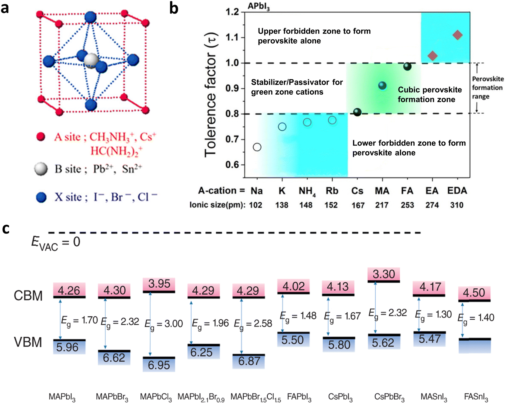 | ||
| Fig. 1 (a) The crystal structure of metal halide perovskite. Reproduced with permission.1 Copyright 2019, American Chemical Society. (b) The calculated tolerance factors (τ) for different cations (A) in the APbI3 perovskite system. Reproduced with permission.3 Copyright 2018, American Chemical Society. (c) The bandgap of ABX3 perovskites with different components. Reproduced with permission.11 Copyright 2022, Wiley-VCH. | ||
A photodetector, as a device that converts optical signals into electrical signals, possesses widespread applications in optical communication,31,32 digital imaging,33–35 bionics,36–38 and artificial electronic skin.39,40 In recent years, metal halide perovskites have revolutionized photodetector performances, such as detectivity,41–43 response speed,44–46 and on/off ratio.47–50 Liu et al. fabricated a flexible planar photodetector based on phenylethylamine lead iodide (C6H5C2H4NH3)2PbI4, which exhibited a large detectivity of up to 1.62![[thin space (1/6-em)]](https://www.rsc.org/images/entities/char_2009.gif) × 1015 Jones.41 Shen et al. reported a broadband vertical photodetector based on MAPbI3 and an organic bulk heterojunction, and an ultrafast response speed of 5.6ns was achieved.44 More importantly, the perovskite materials facilitated the array integration of photodetectors. Array construction of perovskite materials is a prerequisite for fabricating photodetector arrays. Therefore, various kinds of methods for synthesizing perovskite materials with controllable dimensionalities and growth sites have been developed, including one-step or two-step spin-coating methods, spray coating, chemical vapor deposition method, painting method, blade coating method, and so on. Based on the prepared perovskite materials, several types of photodetector arrays have been successfully assembled. Wu et al. reported a split-ring structured CsPbBr3 perovskite photodetector array using dual-function laser etching technology, and successfully demonstrated the potential application in human–machine interactions.51 Huang et al. fabricated a microspectrometer with a pixelated photodetector array based on the graded-bandgap CsPbX3 perovskite, which exhibited a reliable spectral reconstruction performance with a resolution of about 10 nm.52 So far, significant breakthroughs in perovskite-based photodetector arrays have been achieved in flexibility, large-scale integration, multispectral imaging, etc. Therefore, a review is urgently imperative to demonstrate the development of perovskite photodetector arrays.
× 1015 Jones.41 Shen et al. reported a broadband vertical photodetector based on MAPbI3 and an organic bulk heterojunction, and an ultrafast response speed of 5.6ns was achieved.44 More importantly, the perovskite materials facilitated the array integration of photodetectors. Array construction of perovskite materials is a prerequisite for fabricating photodetector arrays. Therefore, various kinds of methods for synthesizing perovskite materials with controllable dimensionalities and growth sites have been developed, including one-step or two-step spin-coating methods, spray coating, chemical vapor deposition method, painting method, blade coating method, and so on. Based on the prepared perovskite materials, several types of photodetector arrays have been successfully assembled. Wu et al. reported a split-ring structured CsPbBr3 perovskite photodetector array using dual-function laser etching technology, and successfully demonstrated the potential application in human–machine interactions.51 Huang et al. fabricated a microspectrometer with a pixelated photodetector array based on the graded-bandgap CsPbX3 perovskite, which exhibited a reliable spectral reconstruction performance with a resolution of about 10 nm.52 So far, significant breakthroughs in perovskite-based photodetector arrays have been achieved in flexibility, large-scale integration, multispectral imaging, etc. Therefore, a review is urgently imperative to demonstrate the development of perovskite photodetector arrays.
In this review, the device types of perovskite photodetectors are firstly introduced, including photoconductors, photodiodes, and phototransistors. Then, the four construction methods of perovskite photodetector arrays are proposed, namely surface treatment technology, template-assisted construction, inkjet printing technology, and modified photolithography. Subsequently, the current development trends of perovskite photodetector arrays in terms of flexibility, large-scale integration, narrowband detection, and bionic structure are summarized, along with their applications. Finally, the remaining challenges for fabricating advanced perovskite photodetector arrays are presented.
2. The fundamental performance parameters of the photodetector device
In order to give a scientific reflection and comparison of the differences between different photodetector devices, some performance metrics are strictly defined to evaluate their performance. In this section, the definition and physical meaning of these fundamental performance parameters of the photodetector device are introduced, respectively.2.1 Responsivity (R)
The R is defined as the ratio of the output signal of the photodetector device to the input light power, which represents the photoelectric conversion efficiency of the photodetector device. The R can be calculated as follows: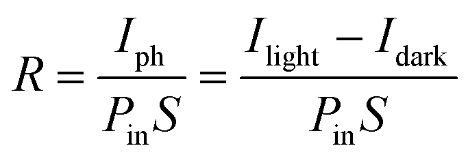 | (1) |
2.2 Specific detectivity (D*)
The D* is defined as the inverse of the noise equivalent power (NEP), which represents the sensitivity of the photodetector device for low signal detection. NEP is defined as the incident light power at the signaltonoise ratio of 1, which refers to the noise current (in) divided by R. The D* can be expressed as follows: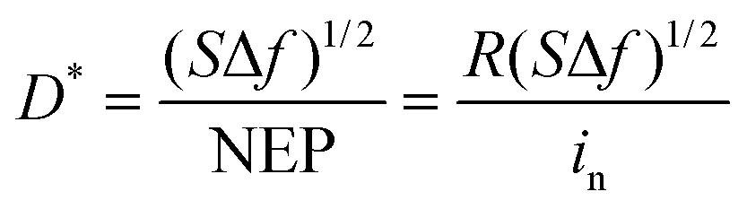 | (2) |
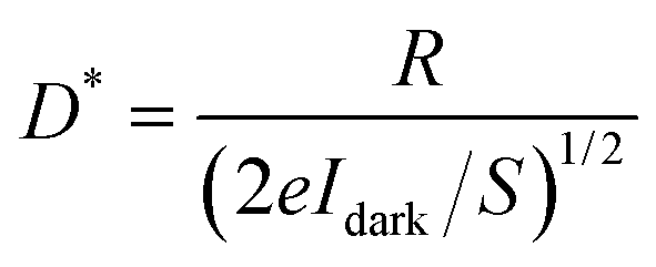 | (3) |
2.3 External quantum efficiency (EQE)
The EQE refers to the average number of electrons released by the photodetector device for each incident photon, which is related to the incident light wavelength (λ). The EQE can be calculated as follows: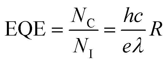 | (4) |
2.4 Linear dynamic range (LDR)
The LDR represents the range in which the photocurrent shows a linear relationship with the incident light density. The formula is as follows: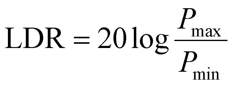 | (5) |
2.5 Response time (τ)
τ reflects the response speed to the incident light of the photodetector device and is classified as the rise time (τrise) and the decay time (τdecay), which are defined as the time for the Ilight to rise from 10% to 90% and decay from 90% to 10% of its maximum value, respectively. In general, the faster the τ of the photodetector device, the more suitable it is for variable light and high time precision detection.2.6 Photoconductive gain (G)
G is defined as the number of carriers passing through the external circuit corresponding to each incident photon in the photodetector device. It can also be calculated by the ratio of carrier lifetime (τl) and transit time between electrodes (τt). The gain is generated when the carrier lifetime is longer than the transit time. G can be calculated as follows: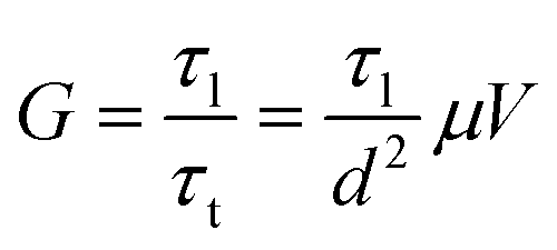 | (6) |
3 Device types of the perovskite photodetectors
The perovskite photodetector arrays are integrated from many individual pixels, and each pixel is a photodetector, whose structural configuration has an important effect on the construction and performance of the final array device. This section introduces the device types of perovskite photodetectors, including photoconductors, photodiodes, and phototransistors.3.1 Photoconductors
Photoconductors have a simple configuration of metal–semiconductor–metal (MSM). According to the position of the electrodes, the perovskite photoconductor can be categorized into planar and vertical structures, as shown in Fig. 2a.53 The working principle is based on the photoconductive effect. The perovskite material absorbs incident photons with an energy higher than the perovskite band gap to produce non-equilibrium carriers. As the carrier concentration increases, the conductivity of the material is enhanced, and current flows through the circuit when an appropriate bias voltage is applied to the device. Perovskite photoconductors with high photoconductive gain and relatively simple fabrication procedures are the most popular types of device structure.54–59 Pan et al. fabricated MAPbI3−xClx films by spin-coating on a patterned gold electrode deposited on the flexible substrate of polyethylene terephthalate (PET), forming a coplanar photoconductor device array with an Au/MAPbI3−xClx polycrystalline film/Au structure, as shown in Fig. 2b.60 This device adopted the interdigital electrode structure, which is widely used in photoconductor devices and can improve the detection signal intensity and signal-to-noise ratio by reducing the electrode distance. The spectral responsivity (R) and detectivity (D*) of this perovskite photodetector array under a 650 nm wavelength light (intensity of 0.033 mW cm−2) were 2.17 A W−1 and 9.4 × 10¹¹ Jones, respectively (Fig. 2c). The on/off current ratio of this photoconductor device increased with the increase of the light intensity, and it followed a linear relationship (Fig. 2d). The response speed of this photoconductor device was evaluated by the rise and decay times, which were 0.48 and 0.26 s, respectively (Fig. 2e). Zhang et al. developed a vertical perovskite photoconductor device with the structure of ITO/CH3NH3PbI3 single crystals/MoO3/Au on the glass supporting substrate (Fig. 2f).61 This device exhibited 88 dB of LDR, high R and D* of 1566–2400 A W−1 and 4.47–6.85 × 10¹² Jones, respectively, in the visible light range at a bias voltage of 2 V and a fixed light intensity of 3 μW cm−2 (Fig. 2g). In addition, we can also notice that a higher electric field can improve the efficiency of photocarrier transmission in the device and the value of R decreases at a higher incident light intensity (Fig. 2h), owing to the saturation of the defect state in the perovskite layer with the increasing incident illumination intensity.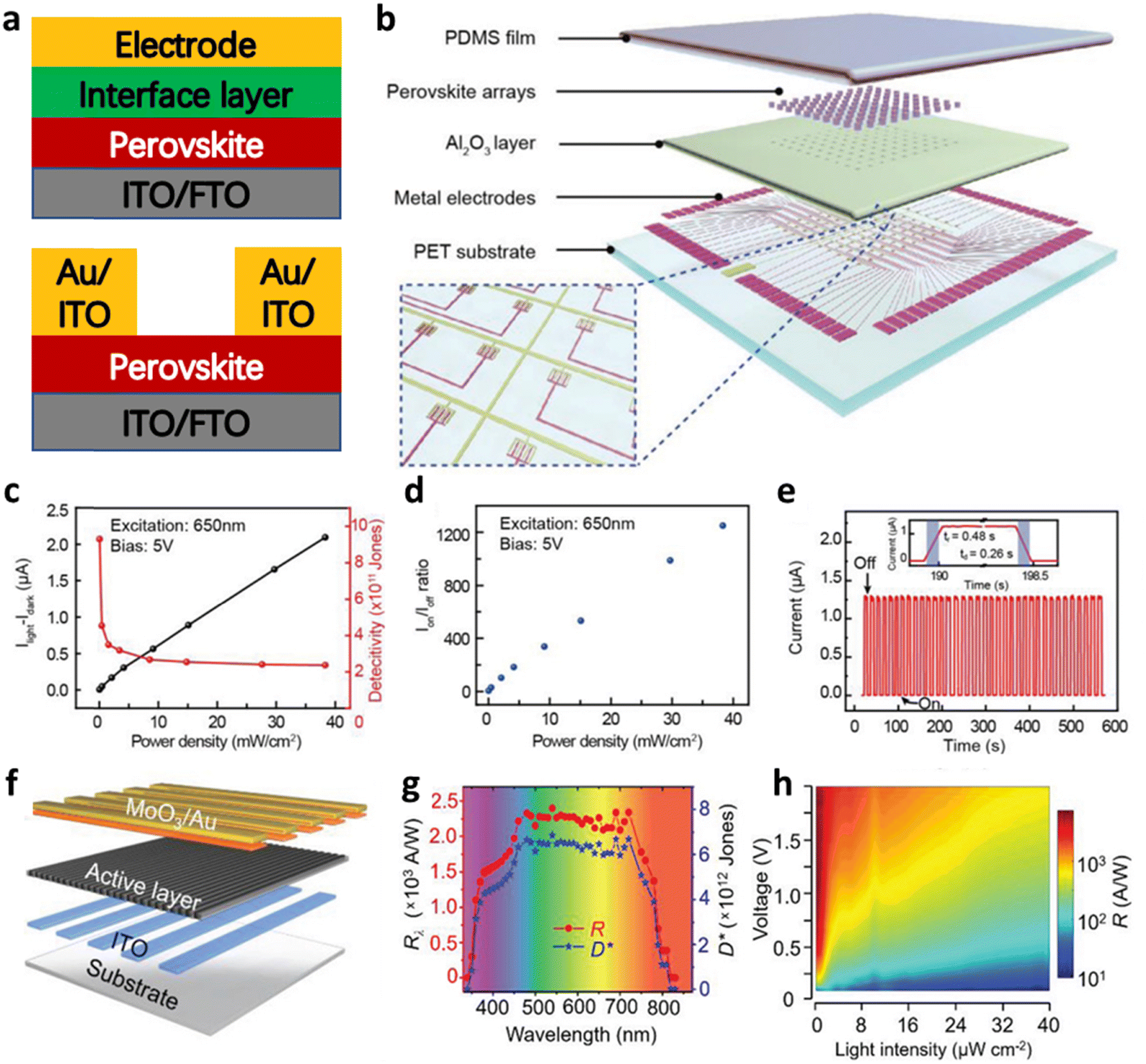 | ||
| Fig. 2 (a) A schematic diagram of the photoconductor device. (b) A schematic structure of the photoconductor detector array device with the inset of the designed complex circuit. (c) The dependence of photocurrent and detectivity under different illumination intensities. (d) The Ion/Ioff ratio of a single pixel under different illumination intensities. (e) The current response of a single pixel under cyclic light on and off. (b–e) Reproduced with permission.60 Copyright 2018, Wiley-VCH. (f) A schematic diagram of the vertically stacked structure of the photodiode array device. (g) The plots of the responsivity and detectivity of the device under different light wavelengths. (h) An image of the variation of the responsivity with incident light intensity and voltage bias. (f–h) Reproduced with permission.61 Copyright 2020, Wiley-VCH. | ||
3.2 Photodiodes
Photodiodes have a vertical structure, in which charge transport materials are applied between the perovskite material and two sides of the electrode to further enhance the composite performance of the detector (Fig. 3a). Photodiodes can work at zero bias voltage due to the built-in electric field that separates the electron–hole pairs generated by the perovskite under photoexcitation and transports them to the corresponding electrodes, resulting in self-powered photodetection.63–66 However, since the photocurrent of the photodiode exhibits a nonlinear characteristic with the light intensity under zero bias voltage,67 it generally works under reverse bias voltage to promote charge collection, which is different from photovoltaic devices.68,69 Compared to planar photodetectors, photodiodes have low dark currents and faster response speeds, benefiting from the carrier rejection mechanism and short carrier transmission distances, respectively. However, due to the lack of inherent gain, photodiodes typically achieve low R and low EQE. Piya et al. developed a self-powered perovskite photodiode device with the structure of FTO/PEDOT:PSS/MAPbI2Br/PCBM/Au on the glass supporting substrate (Fig. 3b).62 The D* of this device was over 1011 Jones in the red light at zero bias, and a narrowband response induced by an unbalanced charge transport in the device was observed (Fig. 3c). This photodiode detector had a low dark current density of ≈10−7 A cm−2 and exhibited an on/off current ratio of over 104 under 625 nm irradiation (≈0.3 mW cm−2) (Fig. 3d). The rise and decay times were 6.88 and 6.58 ms (Fig. 3e), and the response bandwidth was 12 kHz (Fig. 3f), indicating a high response speed of the photodiode device.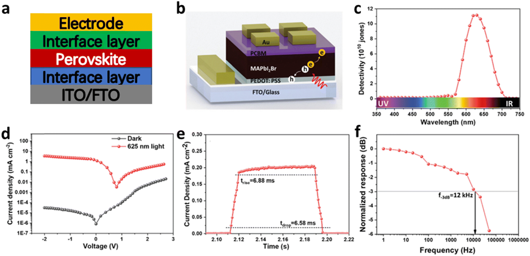 | ||
| Fig. 3 (a) A schematic diagram of the photodiode device. (b) A schematic diagram of the vertically stacked structure of the photodiode device. (c) Specific detectivity spectrum of the photodetector under zero bias. (d) Current density–voltage curve of the photodetector measured in the dark and under 625 nm light illumination. (e) Zoomed view of the current density–time curve during a single light on/off state. (f) Frequency-dependent response spectrum of the photodetector. (b–f) Reproduced with permission.62 Copyright 2020, Wiley-VCH. | ||
3.3 Phototransistors
Phototransistors have a three-terminal device structure, composed of the source (S) and drain (D) electrodes, the photosensitive layer, the gate (G) electrode, and the dielectric layer (Fig. 4a),53 which is similar to the device structure of field-effect transistors (FETs).70 According to the types of channel carriers, the perovskite phototransistors can be classified into n-channel and p-channel devices. When electron–hole pairs are generated within the photosensitive layer of phototransistors due to the absorption of light, one type is trapped on the surface of the semiconductor or in internal defects, and the other type forms a conductive channel.71 The charge transport characteristics in the conductive channel of perovskite phototransistors can be adjusted by the voltage applied to the gate electrode, thereby achieving noise reduction and signal amplification to ensure their excellent performances.72–76 Recently, Zou et al. fabricated phototransistors with a device structure of Au (S&D)/CsPbBr3:P3HT/PMMA/Al (G), whose photosensitive layer was surface-passivated in all-inorganic halide perovskites with poly(3-hexylthiophene) (P3HT) (Fig. 4b).77 The high absorption and fast dissociation of the Frenkel excitons of the hybrid photoactive layer with an optimized energy band structure significantly improved the device performance (Fig. 4c). This phototransistor device exhibited excellent optoelectronic performance under the regulation of the source–drain voltage (VDS) and the gate voltage (VG), which could achieve a relatively high responsivity (469 A W−1), external quantum efficiency (EQE = 1.82 × 10³), and specific detectivity (1.34 × 10¹⁴ Jones) even under a relatively high light intensity (0.4 mW cm−2 under 405 nm illumination) (Fig. 4d–f). In conclusion, perovskite phototransistors can achieve both very high quantum efficiency and responsivity without sacrificing the response speed, combining the advantages of photoconductors and photodiodes.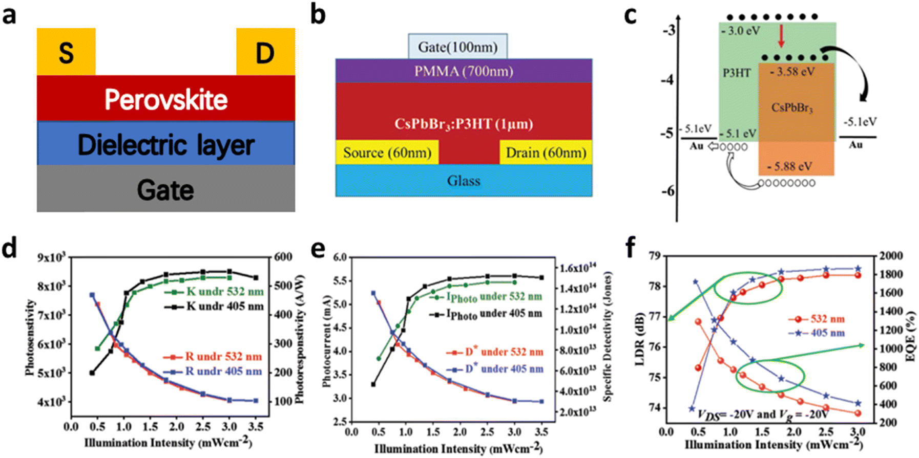 | ||
| Fig. 4 (a) A schematic diagram of the phototransistor device. (b) A schematic structure of the field-effect transistor (FET)-based photodetector with the photoactive layer of CsPbBr3 nanocrystals with poly(3-hexylthiophene) (P3HT). (c) A schematic diagram of the band structure of the hybrid active layer. (d) The photocurrent and detectivity, (e) the photosensitivity and photoresponsivity, and (f) the LDR and EQE of the phototransistor device. (b–f) Reproduced with permission.77 Copyright 2022, Wiley-VCH. | ||
4 Construction methods of perovskite photodetector arrays
A variety of methods for the preparation of metal halide perovskite arrays have been developed based on the solution-processed method or low-temperature vapor deposition method. However, there are still many aspects to be considered in the construction of perovskite photodetector arrays owing to the fragile structure of perovskite materials.78–80 Firstly, to construct perovskite photodetector arrays, the patterned perovskite material generally needs to be grown with precise alignment on the surface of metal electrode materials or other materials such as charge-transporting materials, which has a high requirement for the compatibility of the perovskite material with various interfaces. Second, the fabrication of patterned electrodes for photodetector arrays typically consists of a photolithography process coupled with a metal or semiconductor deposition process, where the solvents used in the development and lift-off process or the high-energy bombardment used in the deposition of metals or semiconductors can cause the degeneration and degradation of the perovskites. Thirdly, so far, efficient and repeatable construction methods of homogeneous perovskite arrays with uniform morphology and performance are rare to meet the demand for large-scale and high-resolution perovskite photodetector arrays. In this section, four effective construction methods of perovskite photodetector arrays are summarized, including substrate surface treatment technology, template-assisted construction, inkjet printing technology, and modified photolithography. The detailed preparation procedures of perovskite photodetector arrays are presented and both the advantages and disadvantages of these construction methods are discussed.4.1 Substrate surface treatment technology
Substrate surface treatment technology refers to the physical or chemical treatment of the surface of the substrate so that the perovskite or its precursor solution can be deposited and grown only in certain areas and not elsewhere.81 Wu et al. reported two-step deposited MAPbI3−xClx film arrays on a substrate by hydrophilic–hydrophobic surface treatment.60 In detail, the Al2O3 film deposited on the PET substrate was first treated with a mixed solution of hexane and (octadecyl) trichlorosilane (OTS) to form a hydrophobic surface. Then, a patterned substrate uncovered with the Al2O3 film was treated by oxygen plasma to form the designed array with a hydrophilic surface, which was processed by UV lithography and etching techniques. In this case, a hydrophilic patterned area was obtained on the hydrophobic surface. Subsequently, a mixed solution of PbI2 and PbCl2 was spin-coated on the as-prepared substrate and immediately followed by a spin-coating of the CH3NH3I solution to convert the precursor arrays into MAPbI3−xClx film arrays. Finally, benefiting from the superior chemical stability and controlled growth of PbX2, it nucleates and crystallizes only in the hydrophilic region and eventually forms a compact film (Fig. 5a). The good crystallinity of the synthesized perovskite arrays was revealed by X-ray diffraction (XRD) measurements after the precursor conversion and annealing process, as shown in Fig. 5b. The scanning electron microscopy (SEM) images of the MAPbI3−xClx film arrays exhibited compact surfaces and clear and uniform shapes at the interface of hydrophilic and hydrophobic regions (Fig. 5c). Large-scale MAPbI3−xClx film arrays with more complex patterns demonstrated the versatility of the construction method (Fig. 5d and e). In addition, patterned perovskite arrays can be aligned with a complex designed circuit by the lithography alignment process during device preparation (Fig. 5f). By combining photolithography and substrate surface treatment processes, it is possible to achieve region-selective growth of perovskite arrays on patterned electrode substrates to fabricate perovskite photoconductor arrays. The size and shape of the pixels can be adjusted by the substrate surface treatment technology to change the resolution of the photodetector arrays. This method is cost-effective, fast, and compatible with a variety of solution-processed perovskites, which is suitable for large-scale fabrication of perovskite photoconductor arrays. The coffee ring effect during the crystallization process on the surface-treated substrate is a major challenge in the fabrication of uniform and dense films, which is mainly caused by uncontrolled droplet diffusion and contact line obstruction.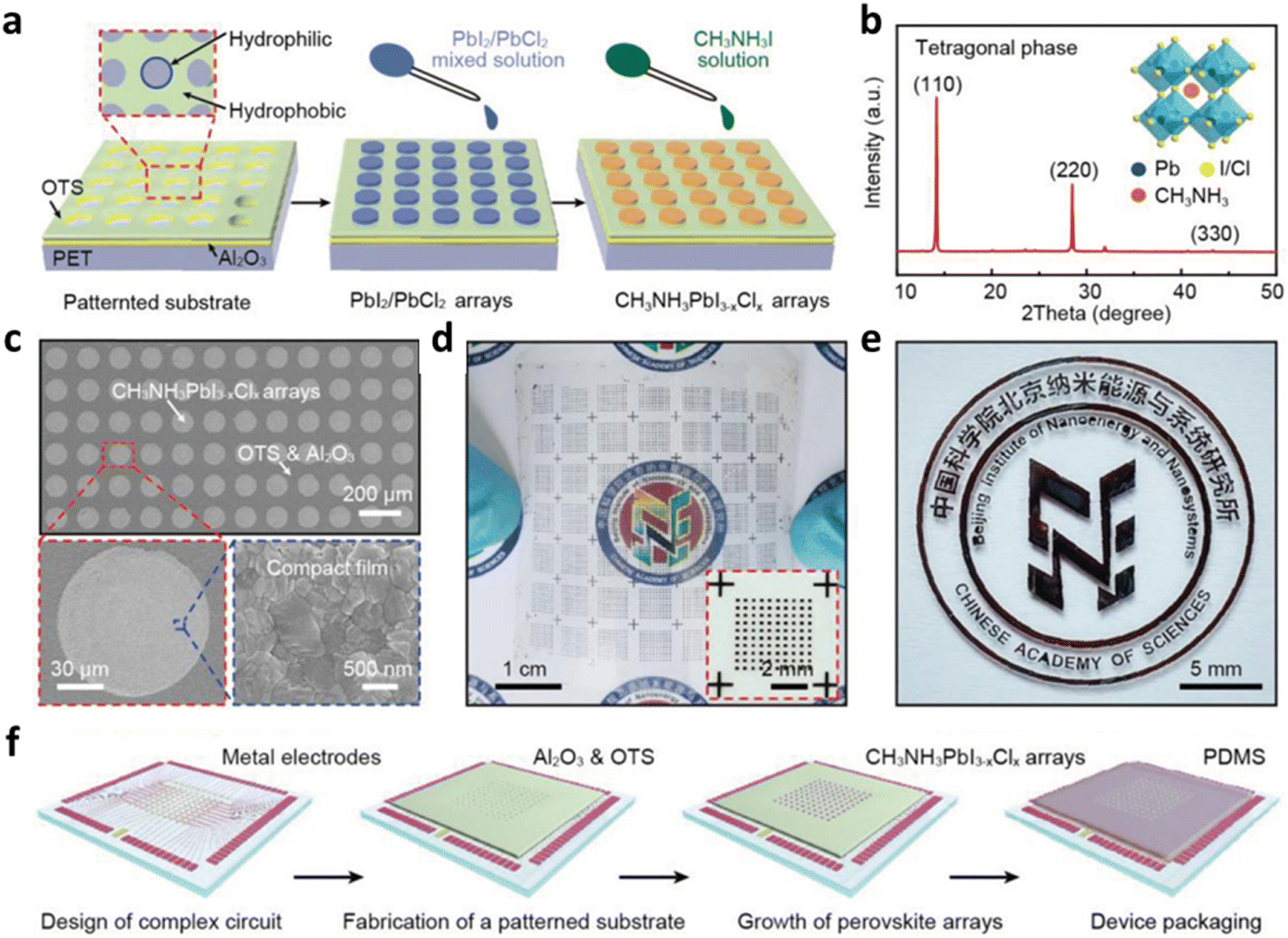 | ||
| Fig. 5 (a) The schematic illustration of the synthesis process of CH3NH3PbI3−xClx arrays. (b) X-ray diffraction (XRD) measurements of the as-synthesized CH3NH3PbI3−xClx arrays. (c) SEM images of patterned CH3NH3PbI3−xClx arrays and the film surface. (d and e) Photographs of large-scale CH3NH3PbI3−xClx film with complex patterns on the PET substrate. (f) A schematic illustration of the fabrication process of the photodetector array device. (a–f) Reproduced with permission.60 Copyright 2018, Wiley-VCH. | ||
4.2 Template-assisted construction
The template-assisted construction method uses a variety of simple templates, such as polydimethylsiloxane (PDMS),82 polymethylmethacrylate (PMMA),83 anodized aluminum oxide (AAO),84 roller and blade coatings,85,86 and photoresist patterns,87etc., to grow geometrically confined perovskite arrays by physically separate precursor solutions. The template-assisted construction method is suitable for the growth of micro and nano single-crystal perovskite arrays. In addition, some templates in this method also act as an insulating layer for the whole device to avoid crosstalk between the perovskite pixels. More importantly, these templates can block the diffusion of water and oxygen molecules, thus reducing the rate of perovskite decomposition and extending the device lifetime. However, the fixed template often limits the construction of photodetector devices with perovskite arrays because of the low pattern resolution of the template, the difficulty of fabricating complex patterns, and the poor alignment with the patterned electrodes. Fortunately, the resolution of the templates can be further improved by advanced micro and nano manufacturing and mark alignment techniques, such as Electron Beam Machining and Ion Beam Machining, etc., leading to high resolution and large-scale perovskite photodetector array devices. Luo et al. reported a template of the patterned PMMA microhole arrays to fabricate the single-crystal MAPbBr3 perovskite microplate arrays.83 As shown in Fig. 6a, traditional photolithography and reactive ion etching technology were used to fabricate the patterned PMMA template. Then, the hydrophobic PDMS was uniformly pressed onto the PMMA template to drive the perovskite precursor solution into the circular PMMA microhole arrays. Finally, rectangular MAPbBr3 microplates were obtained by nucleation growth at the edge of the circular hole with slow evaporation of the solvent. The vast majority of the microplates had a rectangular shape after peeling off the PDMS, except for a few irregular ones that could lead to device malfunction (Fig. 6b). The perovskite photodiode array device with the vertical structure of ITO/MAPbBr3/Au was assembled by using the as-patterned perovskite microplates (Fig. 6c). This template-assisted construction method shows an appeal to be able to integrate large-scale and high-resolution perovskite photodetector arrays due to its merits of combining lithography process patterning. Zhang et al. demonstrated the photoresist patterns as a template for constructing perovskite photodetector arrays combining the blade-coating process.61 First, periodic photoresist microchannels were formed on an indium tin oxide (ITO)-glass substrate by photolithography. Then, the perovskite solution was dragged over these photoresist microchannels with a blade at an optimized deposition rate and temperature. The microchannels were then all filled with the perovskite solution driven by capillary force. Finally, as the solvent evaporated from the perovskite solution inside the microchannels, the perovskite molecules precipitated and formed seed crystals, which continued to grow and eventually formed single-crystal perovskite (Fig. 6d). Real-time observation of the crystallization process by cross polarized optical microscopy (CPOM) showed that the single-crystal CH3NH3PbI3 arrays were neatly arranged within the microchannel array due to the well-controlled solution flow dynamics (Fig. 6e). The detailed geometrical appearance of the CH3NH3PbI3 perovskite single crystals indicated that it was filled into the microchannels (Fig. 6f and g). Based on the embedded structure of CH3NH3PbI3 perovskite, a vertical-type photodetector array was fabricated by using stainless-steel shadow mask deposition of top electrode arrays (Fig. 6h and i). In this device, the photoresist pattern served as both a template for material preparation and an insulating layer to prevent short circuits between the top and bottom electrodes.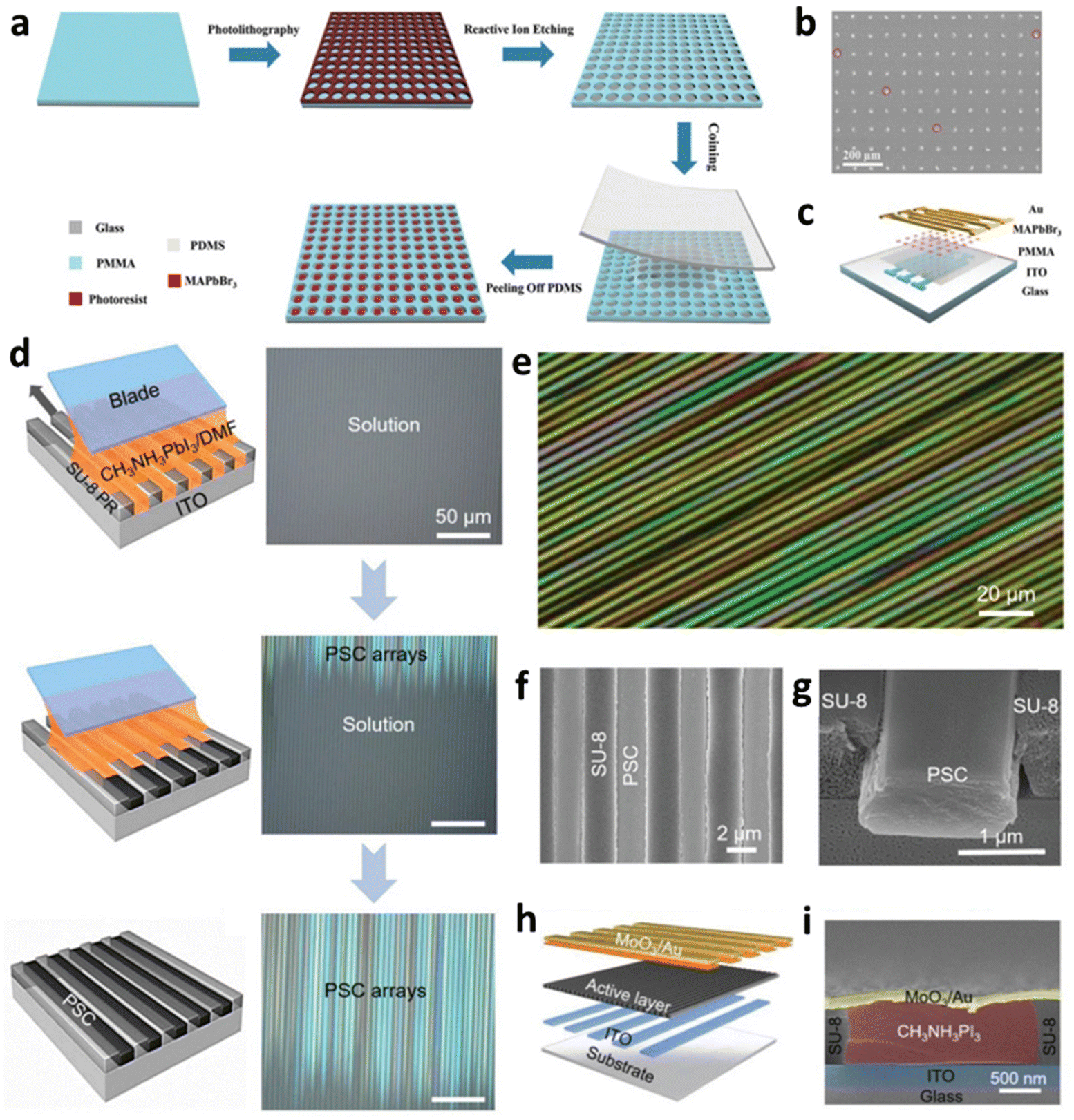 | ||
| Fig. 6 (a) A schematic illustration of the fabrication process of the patterned perovskite single crystal (PSC) arrays based on MAPbBr3. (b) A SEM image of the MAPbBr3 single crystal arrays. (c) A schematic illustration of the device structure of the MAPbBr3 photodetector array. (a–c) Reproduced with permission.83 Copyright 2021, Wiley-VCH. (d) A schematic illustration of the blade coating process by the microchannel confined crystallization (MCC) strategy. (e) A cross-polarized optical microscopy (CPOM) image of the MAPbBr3 PSC arrays at 45° rotation angle. (f) A SEM image of the MAPbBr3 PSC arrays. (g) A cross-sectional SEM image of a single MAPbBr3 PSC. (h) A schematic illustration of the image sensor with vertically stacked structure. (i) A cross-sectional SEM image of a single pixel. (d–i) Reproduced with permission.61 Copyright 2020, Wiley-VCH. | ||
4.3 Inkjet printing technology
Inkjet printing is a non-contact, micron/nano-scale material preparation technology.88 Typically, inkjet printing can be divided into two printing modes, namely piezoelectric inkjet and thermal inkjet.89,90 Inkjet printing equipment includes an ink cartridge and an inkjet head capable of depositing the solution precisely over the designed area. Because the execution of this technology does not need complex micromachining processes, inkjet printing is considered a simple and efficient approach to fabricate perovskite photodetector arrays.91,92 Huang et al. introduced an electrohydrodynamic (EHD) printing process to directly fabricate different types of perovskite films into a photodetector array device for full-color imaging.93 It consists of three steps, namely printing, in situ precrystallization, and post-annealing. First, the ionic liquid methylammonium acetate (MAAc) solvent was used to reduce the crystallization rate of perovskite inks so that the resulting perovskite film had regular morphology and credible performance. Then, droplets were formed on the substrate by applying a high pulsed voltage between the glass nozzle and the grounded substrate to overcome the surface tension of the meniscus (Fig. 7a). Finally, the photoconductor array device with Cr/Au/MAPbX3 polycrystalline film/Au structure was fabricated (Fig. 7b). A pulse voltage was used in which the jetting of the EHD printing process started from the peak voltage (Vp) and stopped at the baseline voltage (Vb) (Fig. 7c). The average diameter of the printed pixel dots increased linearly with the increase in Vp, as the higher electric field strength provided greater jet power, and decreased with the pulse frequency due to the shorter jetting time (Fig. 7d). The surface of the perovskite film formed by the ink using dimethylformamide (DMF) as the solvent had many hole defects, while the surface of the perovskite film formed by the ink using MAAc solvent is flatter, indicating that the selection of a suitable solvent of the perovskite is crucial for the quality of printed films (Fig. 7e and f). Precise drop-on-demand printing can be achieved by adjusting several key factors including the pulse voltage, nozzle diameter, and printing distance, to match the properties of different perovskite inks (Fig. 7g and h).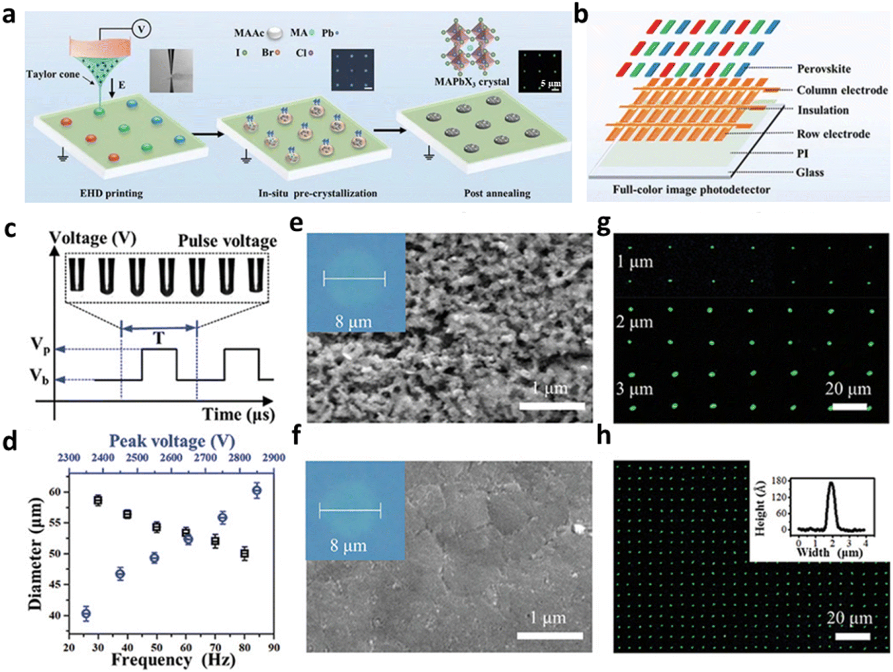 | ||
| Fig. 7 (a) A schematic illustration of the EHD printing and perovskite transformation process. (b) A schematic illustration of the structure of the perovskite image photodetector array device. (c) The pulse voltage used in EHD printing and the shape changes of the solution at the nozzle tip within one cycle. (d) The relationship between MAPbX3 dot diameter and pulse frequency or peak voltage. (e and f) SEM images of printed MAPbI2.4Br0.6 films with two different solvents (DMF and MAAc) of inks. (g) The high-resolution dot array by the EHD printing with dot diameters of 1, 2, and 3 μm respectively. (h) The EHD printed high-resolution dot array with a diameter of ≈1 μm. (a–h) Reproduced with permission.93 Copyright 2021, Wiley-VCH. | ||
Inkjet printing is also a very promising technology for commercial applications in low-cost, high-volume printed electronics due to ease of patterning, high material utilization, and non-polluting non-contact deposition. However, there are so many parameters that affect the quality of the film and the resolution of the array, including ink jet characteristics, solution evaporation behavior, ink viscosity, and nozzle diameter. At the same time, the coffee ring effect after solution deposition is also a major challenge in producing uniform and dense films using inkjet printing technology.94–96 Currently, various techniques are being introduced into the inkjet printing process to improve the quality of inkjet-printed films, which are as follows: (1) ink design, using low surface tension materials (surfactants, dodecanethiol), high boiling point solvents, gelled polymers, or modified nanoparticles; (2) substrate treatment, improving substrate surface wettability, reducing surface temperature, or introducing corona treatment; (3) equipment improvements, such as customized nozzle diameters or improved planar shift accuracy. The above methods are effective in improving the shape, thickness, and morphology of dried microdroplets, as well as the precision of the printed film.97
4.4 Modified photolithography
Photolithography is an important step in the semiconductor device manufacturing process that uses exposure and development to etch geometric patterns on a photoresist layer, and then transfers the pattern on the photomask to the substrate by an etching or ion sputtering process. However, perovskite materials are incompatible with such high-resolution patterning lithography methods due to their degradation in photolithographic polar solvents and poor thermal stability,98–100 which hinders perovskite patterning and device integration. Therefore, some modified photolithography processes have been developed to solve the above problems, including using a well-designed photoresist, adding a protective layer, and accepting the lift-off process.101–104 In addition, some direct lithography processes have also been applied to the high-resolution and large-scale fabrication of perovskite arrays.105–107 Yang et al. reported a photocatalysis of lead bromide complexes to support the patterning of different types of perovskite quantum dots.105 Liu et al. introduced the underlying, non-specific ligand cross-linkers that allow for the high-fidelity and multi-color patterning of a wide range of perovskite nanocrystals with their native ligands.106 Liang et al. presented a femtosecond laser direct writing method suitable for high-resolution patterning of various sizes of 2D perovskite film arrays.107 In brief, most of the modified lithography techniques are only applicable to one or a few types of perovskite array growth. Therefore, the development of improved modified lithography processes applicable to most of the perovskite arrays and different types of device preparation will be a promising direction for researchers' attention. Ren et al. fabricated a wafer-scale photoconductor array device with the Cs2AgBiBr6 perovskite material using photolithographic patterning method, whose strategy was to remove the degradation layer after photolithography (Fig. 8a and b).108 First, a full side of Cs2AgBiBr6 film was fabricated by the optimized antisolvent method, which exhibited compact and pinhole-free morphology and high phase purity (Fig. 8c). Then, the Cs2AgBiBr6 film was patterned by a photolithography process with a commonly used photoresist and developer reagents, which caused the degradation of the pale surface layer of the Cs2AgBiBr6 perovskite film (Fig. 8d). Then, the HBr solution treatment based on the Lewis acid–base interaction separated the degradation layer, resulting in a high-quality photolithography patterned film with a steep edge and flat etched area (Fig. 8e and f). S. J. Oh et al. introduced an all-solution two-step patterning method for preparing cesium lead halide perovskite (CsxPbyBrz), which was designed to be compatible with the existing photolithography equipment.109Fig. 8g showed the patterning process of the patterned CsxPbyBrz. Briefly, the PbBr2 film was first deposited on a substrate by a spin-coating method. Then, the photoresist was spin-coated over the PbBr2 film and exposed under the 365 nm ultraviolet light through a patterned photomask. The patterned PbBr2 was achieved by the simultaneous development and etching process using tetramethy-lammonium hydroxide (TMAH) and deionized water (DI), which had the selective etching ability to etch only PbBr2 and the UV-exposed photoresist (Fig. 8h). Subsequently, the patterned PbBr2 film was transformed into CsxPbyBrz by dipping into the CsBr solution with the control of reaction time and concentration. Finally, the perovskite array without impurities was fabricated after removing the residual CsBr by an IPA-assisted reaction due to its excellent rinsing function (Fig. 8i and j). Photoconductor arrays were successfully fabricated by the optimized photolithography process to precisely align the patterned CsPbBr3 array with patterned metal electrodes (Fig. 8k).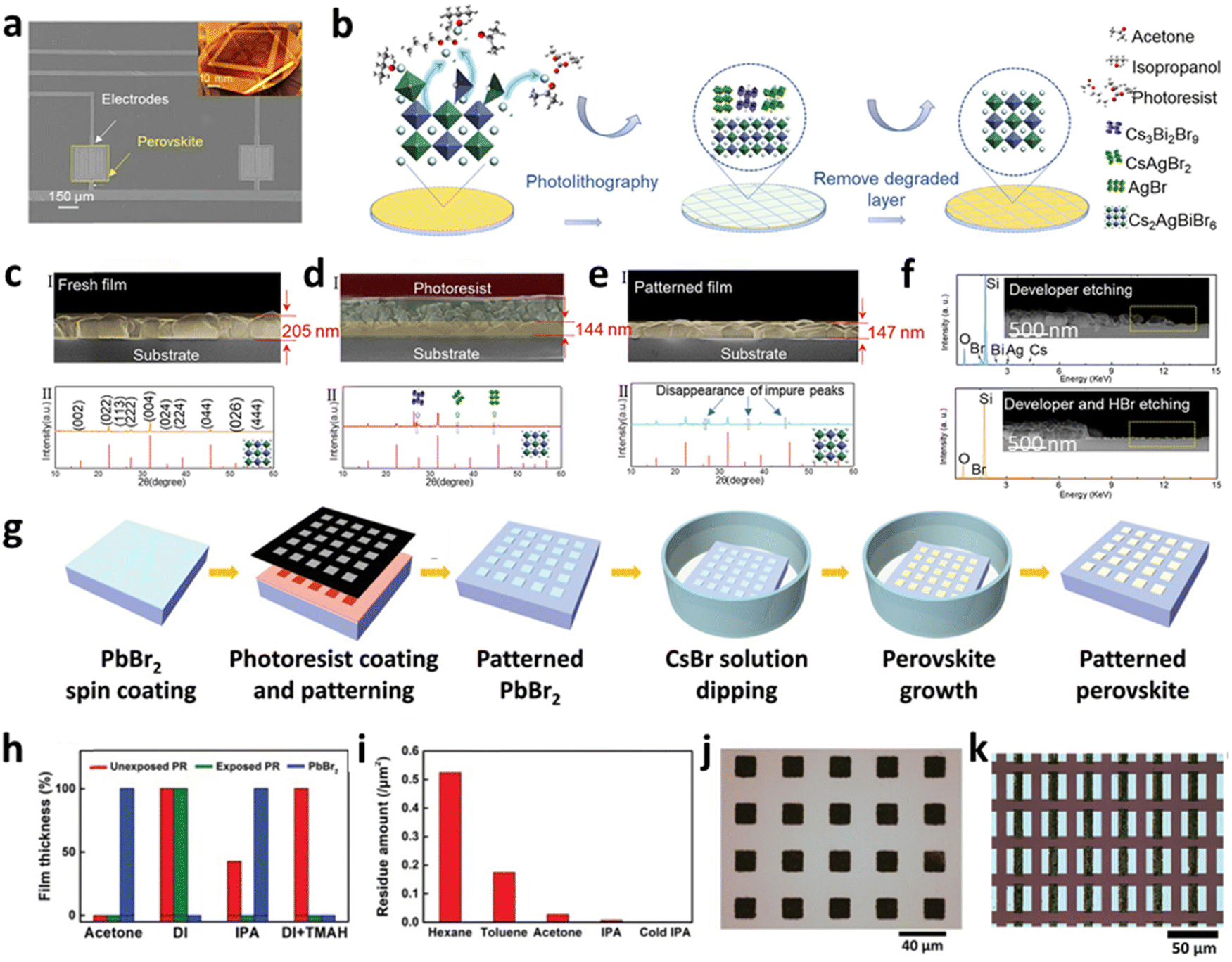 | ||
| Fig. 8 (a) A SEM image of a pixelated Cs2AgBiBr6-based device and the inset of electrode arrays on an oxide silicon wafer. (b) The modified photolithography process and the corresponding material structures at different stages. (c–e) A cross-sectional SEM image (I) and XRD peaks (II) of fresh Cs2AgBiBr6 film (c), Cs2AgBiBr6 film with photoresist (d), and the terminal patterned Cs2AgBiBr6 film (e). (f) Cross-sectional SEM images of the edge of the patterned Cs2AgBiBr6 film before and after HBr treatment with energy dispersive X-ray spectroscopy (EDS) analysis of the marked areas, respectively. (a–f) Reproduced with permission.108 Copyright 2022 American Chemical Society. (g) A schematic illustration of the PbBr2 patterning and perovskite transformation process. (h) The film thickness after different solvent treatment of the photoresist and PbBr2 film. (i) The residues amount in the patterned perovskite by different solvents. (j) An optical image of the patterned perovskite rinsed by −20 °C IPA. (k) An optical image of the CsPbBr3 photoconductor array. (g–k) Reproduced with permission.109 Copyright 2022, Wiley-VCH. | ||
5 Development trends and applications of perovskite photodetector arrays
Metal halide perovskites are expected to be the new generation of low-cost and high-performance materials to promote the development of photodetectors in imaging, machine vision, and optical communication. This section presents the current development trends of perovskite photodetector arrays in terms of flexibility, large-scale integration, narrow-band detection, and bionic structure, and at the same time, introduces the corresponding applications.5.1 Flexible perovskite photodetector arrays
In recent years, flexible electronic devices have attracted great attention as one of the future development directions. The rapid development of flexible processing technology has led to the gradual evolution of electronic devices from the previous rigid systems to flexible systems.110–113 Flexible perovskite photodetector arrays have great potential in bionics and artificial electronic skin for photosensing and imaging applications.114–116 For the assembly of flexible photodetector arrays, substrate materials should have the characteristics such as flexibility, insulation and corrosion resistance, and chemical and thermal stability. These commonly available materials are polyvinyl alcohol (PVA), polyester (PET), polyimide (PI), polynaphthalene dimethyl ethylene glycol (PEN), textile materials, etc.52,118–121 Huang et al. introduced a flexible 10 × 10 perovskite photodetector array on the PI substrate by developing inkjet printing technology for color detection.93 Each pixel with a photoconductor structure of Au/perovskite/Au consisted of three sub-pixels. The bending test of the device at different bending angles was performed to verify the mechanical stability (Fig. 9a). The photocurrent of this flexible device decreased within a controlled range of ∼8% as the bending angle increased from 0° to 150° (Fig. 9b). Furthermore, the I–V curve of the flexible device remained essentially unchanged after a maximum of 500 cycles under the bending angle of 60°, demonstrating high robustness (Fig. 9c). In addition, this flexible perovskite photodetector array device can be easily and completely attached to curved surfaces (Fig. 9d). Wu et al. also reported a photoconductor array device composed of 10 × 10 pixels with excellent flexibility for imaging.117 The ultrathin parylene-C film was used as the supporting substrate and packaging materials, and thin CsPbBr3 perovskite films were employed as the photosensitive materials. This ultrathin device could be conformed to irregular surfaces without damage. As displayed in Fig. 9e, it was able to adhere to the wrinkled human skin surface without delamination from it after being compressed, demonstrating the unprecedented flexible characteristic. The photoresponse remained stable under different compressive strains, revealing superior mechanical robustness. Imaging tests were performed by irradiating a patterned light source onto an ultrathin device mounted on a hemispherical holder. The clear letters of ‘H’, ‘N’, and ‘U’ could be recognized from the current mapping, illustrating the reliable imaging capability of the flexible device on curved surfaces (Fig. 9f).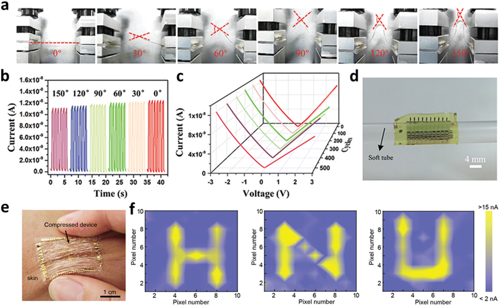 | ||
| Fig. 9 (a) Photographs of the photodetector array device bent at different angles from 0° to 150°. (b) The photoresponse of the device at different bending angles. (c) I–V curves of the device after different bending cycles. (d) An optical photograph of the flexible photodetector array device. (a–d) Reproduced with permission.93 Copyright 2021, Wiley-VCH. (e) A photograph of the laminated ultrathin device being compressed on the human skin. (f) Photocurrent distribution images obtained by lamination detection of photodetector arrays on hemispherical brackets with ‘H’, ‘N’ and ‘U’ letter masks. (e and f) Reproduced with permission.117 Copyright 2021, Wiley-VCH. | ||
5.2 Large-scale perovskite photodetector arrays
Large-scale integration of perovskite photodetectors is the basis for achieving high-resolution image sensing, which is an important part of the commercialization of perovskite photodetectors. The efficient preparation processes of large-scale perovskite arrays with homogeneous properties are the most important factors for obtaining large-scale perovskite photodetector arrays. Zhang et al. reported large-scale photodetector arrays with vertical device structures based on homogeneous CH3NH3PbBr3 single-crystal microplates (Fig. 10a).122 Through a substrate surface treatment process to suppress the multiple nucleation, the CH3NH3PbBr3 single-crystal microplate was only grown on the surface of patterned gold nanoparticles. Thus, the large-scale perovskite single-crystal microplates with uniform morphology and crystalline quality were obtained (Fig. 10b), which provided useful support for the subsequent integration of photodetector arrays. The performance uniformity of the pixels in the photodetector arrays is fundamental for large-scale imaging applications. The dark currents and photocurrents (light intensity of 109 μW cm−2) of all pixels were statistically found to be distributed within a narrow range, and the ratio of the standard deviation of the photocurrents to the average value was less than 5.2%, indicating that the performance uniformity of this 10 × 10 array device was credible (Fig. 10c). Because the pixels are addressed independently, the patterns both with simple and complex outlines can be imaged by the perovskite arrays (Fig. 10d and e). Xia et al. fabricated a flexible photodetector array with a van der Waals MAPbI3/graphene heterostructure as the photosensitive layer for large-scale (24 × 24 pixels) imaging (Fig. 10f).123 This device showed excellent flexibility (Fig. 10g) and an ultra-high responsivity of 107 A W−1. Two-dimensional current mapping displayed clear images with patterns of a cartoon pig and the QuickMark code, demonstrating the excellent imaging capabilities of this large-scale perovskite photodetector array (Fig. 10h).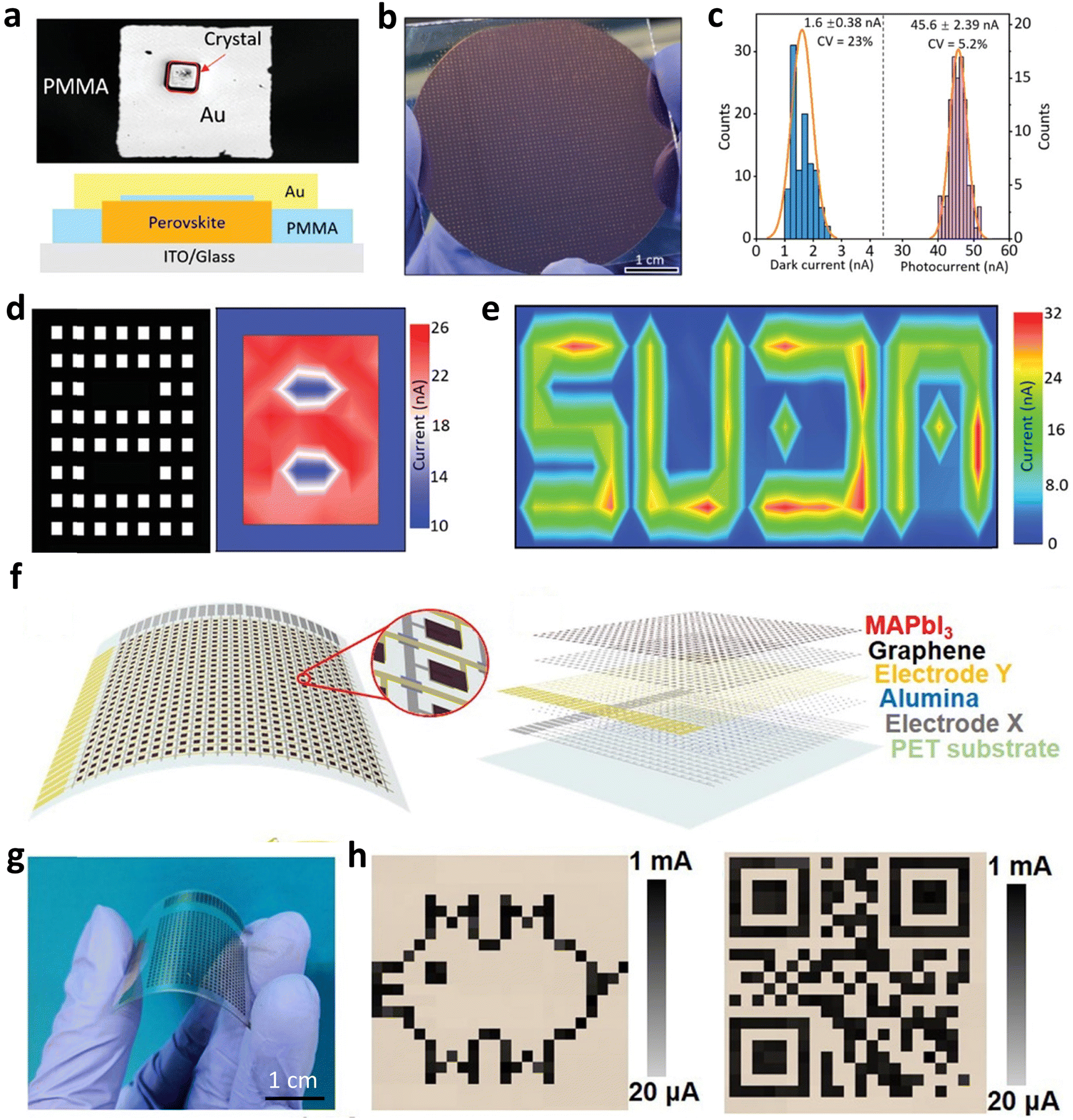 | ||
| Fig. 10 (a) Three-dimensional (3D) surface topography image and corresponding schematic of the device. (b) Digital photograph of patterned single-crystal perovskite microplates on a 2 inch silicon wafer. (c) Distribution of the dark current and photocurrent of the perovskite microplate array device. (d) A photocurrent image of the photodetector array with an ‘8’-shaped mask under white illumination. (e) A reconstructed photocurrent image of ‘SUDA’ by the photodetector array. (a–e) Reproduced with permission.122 Copyright 2022, Wiley-VCH. (f) A schematic illustration of the flexible 24 × 24 image sensor array device on PET substrate. (g) Photograph of a flexible image sensor. (h) The corresponding output images of a cartoon pig and the QuickMark code of ‘photodetector’ under light illumination (30 mW cm−2, 633 nm). (f–h) Reproduced with permission.123 Copyright 2019, Science China Press. | ||
5.3 Narrowband perovskite photodetector arrays
The narrow-band photodetector arrays have a selective response to photons of different wavelengths, which is similar to the functions of cones in the retina and plays an essential role in the human–machine visual interaction systems. Recently, narrowband detection has become a development direction of perovskite photodetector arrays for multispectral imaging.124 The common ways to realize a narrow spectrum response include (i) using materials with narrow-band absorption or enhancing the absorption of materials at specific wavelengths by plasmon resonance; (ii) coupling broadband photodetectors with bandpass filters or optical microporous structures; (iii) using charge collection narrowing (CCN) mechanisms to modulate the quantum efficiency.36,125,126 For perovskite materials, the last two methods are usually used to achieve the construction of narrow-band photodetector arrays. As for the second method, it increases the complexity of the device structure and the fabrication cost by adding additional filters. The CNN mechanisms can regulate the light distribution in the active layer by adjusting the thickness of the perovskite film, which in turn can select the desired detection band and realize the charge narrowing absorption effect, thus achieving selectable detection bands with narrower half-wave peak widths. At the same time, the use of thick junctions reduces the defect density and thus significantly suppresses the dark current, resulting in a higher specific detection rate and LDR. Therefore, researchers prefer this method to prepare narrow-band photodetector arrays.Chen et al. successfully fabricated a CsPbBr3 photodetector array with an ultra-narrow spectral response by a freeze-drying casting method.127 This designed 10 × 10 perovskite photodetector array device was fabricated with the photodiode structure on the glass substrate (Fig. 11a and b). As shown in Fig. 11c, as the thickness of the CsPbBr3 film increased, the spectral response in the short wavelength region gradually decreased, which was caused by the CCN mechanism. The light in the short wavelength region had a carrier on the top of a thick CsPbBr3 film. The photogenerated carriers would be quenched by recombination before diffusing to the collecting electrodes (Fig. 11d). A narrowband response with a full-width at half-maximum (FWHM) of less than 12 nm occurred near the absorption cutoff of the CsPbBr3 film. The image of the photocurrent/dark current ratio showed a uniform photoresponse of this array device under white light illumination, demonstrating the good consistency among the individual pixels. Furthermore, this device output an image with a dark identifiable ‘N’ shape under the monochromatic light of 610 nm, while a bright identifiable ‘N’ pattern was displayed under the monochromatic light of 540 nm due to its different responsivity at different wavelengths of monochromatic light (Fig. 11e). In addition, narrow-band photodetectors with different bandgap materials (CsPbClBr2, CsPbBr3, and CsPbBr1.5I1.5) were fabricated and alternately arranged in rows to form a new array device for real-time imaging. When illuminated by three strip light sources with different wavelengths arranged in columns, this array device responded only to the light within its narrowband spectral detection range (Fig. 11f). The above results demonstrated the reliable imaging function with spectral selectivity of these narrow-band photodetector arrays. By modulating the photon absorption and charge collection, the perovskite photodetector arrays with continuously tunable detection bands are desirable.
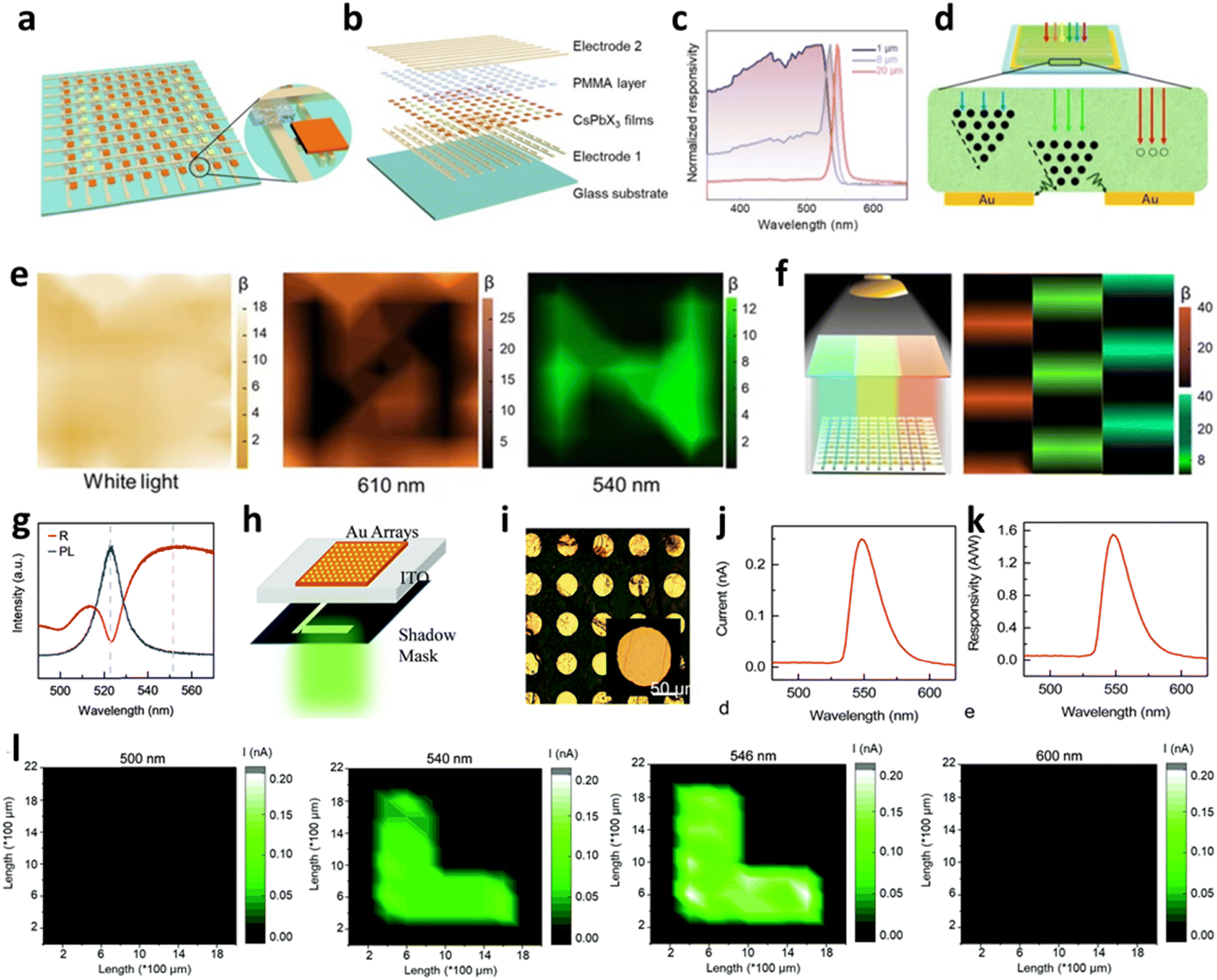 | ||
| Fig. 11 (a) A schematic illustration of the 10 × 10 perovskite photodetector array. (b) The schematic structure of the 10 × 10 perovskite photodetector array. (c) The EQE spectra of CsPbBr3 films under different thicknesses. (d) A schematic mechanism of the surface charge recombination assists narrow-band photodetector. (e) The output images of the 10 × 10 perovskite photodetector array with a mask of the letter ‘N’ under the illumination of white light, 610 nm, and 540 nm. (f) A schematic illustration of the photodetector array device under the illumination of different colors and the corresponding output images. (a–f) Reproduced with permission.127 Copyright 2018 American Chemical Society. (g) The PL and reflection spectra of the (BA)2PbI4 2D perovskite plates. (h) The structure schematic of the (BA)2PbI4 narrowband photodetector array device with a shadow mask with the letter ‘L’. (i) AN optical image of the (BA)2PbI4 narrowband photodetector array and a single Au spherical film. (j) The device current and (k) the responsivity under different wavelengths of light. (l) Current images of the (BA)2PbI4 narrowband photodetector arrays under four different wavelengths of light. (g–l) Reproduced with permission.128 Copyright 2021 the Royal Society of Chemistry. | ||
Li et al. demonstrated a 12 × 11 narrowband photodetector array based on (BA)2PbI4 2D single crystals for imaging.128 The PL and reflection spectra of the synthesized 2D perovskite plates showed one emission peak at around 522 nm and two reflection peaks at around 514 nm and 551 nm at room temperature, which can be attributed to the free and self-trapped excitons (Fig. 11g). The narrowband photodetector arrays were constructed with a vertical structure of ITO/(BA)2PbI4 2D single crystal plate/Au (Fig. 11h and i). This device exhibited narrow band photoresponse characteristics with a FWHM of 24 nm at the peak of around 546 nm (Fig. 11j), whose working mechanism was based on the CCN concept together with structure self-trapped states. It also exhibited an estimated maximum responsivity of 1.53 A W−1 (Fig. 11k) and a high external quantum efficiency of 350% under 546 nm illumination. The 12 × 11 (BA)2PbI4 narrowband photodetector arrays also showed excellent wavelength discrimination performance. When four monochromatic lights of different wavelengths with approximately the same power density were projected from the back of the device through the shadow mask onto the device, only the light illumination with wavelengths (540 nm and 546 nm) in the narrow-band detection range could be detected by the device. Light illumination with wavelengths (500 nm and 600 nm) outside the narrow-band detection range could not be detected, resulting in a black image without any pattern (Fig. 11l). The output photocurrent under 546 nm illumination was obviously larger than that under 540 nm illumination due to the different spectral response and both of them showed the image with a clear letter ‘L’, indicating the excellent wavelength selection of this perovskite narrowband photodetector array.
5.4 Bionic perovskite photodetector arrays
Some organisms have functions that are far superior to any man-made machine, such as information reception (sensory function), information transmission (neural function), automatic control systems, etc. The imitation of these state-of-art biological functions has promoted the development of bionics.129–134 In the field of optical sensing and imaging, photodetectors with some bionic structures have been applied to manufacturing, such as an optical element of the fly eye lens in imitation of the compound eye of a fly, which consists of hundreds or thousands of small lenses neatly arranged and combined.135 It is capable of taking thousands of the same photo at a single time, which has been used for printing plates and projection display, greatly improving the efficiency and quality. In recent years, innovative perovskite photodetector arrays have been used to mimic the visual functions of the human eye, such as color recognition and curved surface imaging, which have wide applications in visual sensing of bionic robotics and human–computer interaction.38,136 The geometric shape of the perovskite photodetector arrays is vitally concerned in the bioinspired sensing system. Compared to a planar image sensor, a curved image has the advantages of reducing the number of optical elements, correcting aberrations including astigmatism and coma, and increasing off-axis brightness and sharpness.37,137 However, the commercial image sensors, such as charge-coupled device (CCD) and the complementary-metal-oxide-semiconductor (CMOS), are mainly planar structures and are fabricated by universal planar microfabrication processes, making it a tremendous challenge to integrate flexible perovskite photodetector arrays into curved or even spherical surfaces. Due to the simple solution preparation process of perovskites, integrated curved or even spherical photodetector arrays can be obtained by inkjet printing through direct spraying of perovskite on curved surfaces or by template-assisted deposition of perovskite in spherical templates. In addition, curved photodetection can also be achieved by transferring some flexible planar devices onto curved surfaces with some special device structures, such as origami structure, kirigami structure, island-bridge structure, fractal web structure, etc., which are designed to reduce or eliminate the stress on the perovskite material to ensure the device performance in the curved or even spherical surfaces.Fan's group displayed a biomimetic eye with a high-density formamidinium lead iodide perovskite nanowire array grown inside a hemispherical porous aluminum oxide membrane (PAM) to mimic the photoreceptors on the human retina.138 Thin liquid–metal wires were used as nerve fibers to connect the biomimetic eye to a computer-controlled multiplexer to form the measurement system. Since adjacent pixels were isolated from each other, this device provided an excellent imaging capability, with high contrast and clear edges of the mask with the letter ‘A’. Taking advantage of the hemispherical shape of the biomimetic array device, it could achieve a wider field of view (FOV) and better focus light on each pixel compared to a planar device, which benefited from the more uniform distance between pixels and the lens. Moreover, the FOV of the hemispherical photodetector array device can be further improved by optimizing the distribution of the photosensitive perovskite pixels. Wei et al. demonstrated hemispherical photodetectors with the structure of Cr/PEDOT:PSS/PEA2FAn−1PbnX3n+1/C60/BCP/Cr by spray-coating methods (Fig. 12a).139 By adjusting the halide I/Br ratios of the employed perovskite films, these devices could obtain clear swan patterns with a narrow-band photoresponse on hemispherical surfaces (Fig. 12b). In addition, the hemispherical perovskite photodetector device showed approximately the same photocurrent at different light incidence angles from 0° to 90° (Fig. 12c). By removing the light source of the imaging system, the same clear swan patterns were obtained at different angle ranges, achieving wide-angle imaging of 180°, as demonstrated in Fig. 12d. However, since the photocurrent of the planar device decreased linearly with increasing angle of incidence until it was almost undetectable at 90°, the swan pattern obtained by the planar device was partially missing in a wide-angle range. Meanwhile, a 9 × 9 hemispherical photodetector array device was also fabricated by spray-coating, and a microarray image perfectly showed the shape of the object, proving its excellent imaging capability (Fig. 12e and f).
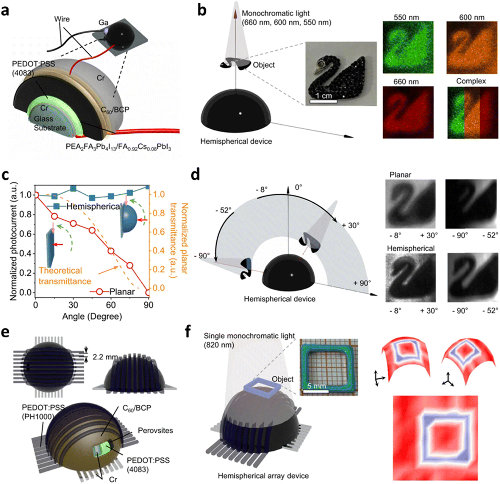 | ||
| Fig. 12 (a) A schematic of the structure of the hemispherical perovskite photodetector device. (b) A schematic of the imaging system and the swan images captured by the hemispherical device with different I/Br ratios. (c) The photocurrent of the hemispherical and planar perovskite photodetector devices under different light angles. (d) A schematic of the imaging system for wide angle detection and the images detected by planar and hemispherical photodetectors under different light angles. (e) A schematic of the structure of a 9 × 9 hemispherical perovskite photodetector array device. (f) A schematic of the imaging system for the hemispherical array device and the microarray imaging result. (a–f) Reproduced with permission.139 Copyright 2022, Springer Nature. | ||
6 Conclusion and outlook
Metal halide perovskite materials have been used as light-harvesting materials in photodetectors due to their low-cost solution fabrication process and remarkable optical and electrical properties. Metal halide perovskite photodetector arrays show great potential for high-performance image sensing applications. In this review, we reviewed the types of perovskite photodetectors, and introduced the recent effective ways to construct perovskite photodetector arrays along with their future development trends.According to the device configuration, perovskite photodetectors can be divided into three types: photoconductors, photodiodes, and phototransistors. The different device structures result in differences in their optoelectronic performance. In general, photoconductors have a higher gain and external quantum efficiency than photodiode detectors, but photodiodes have lower dark currents and faster response speeds. Phototransistors have the performances that combine the advantages of both. In terms of array device construction methods, surface treatment and template-assisted construction methods are considered as the bottom-up construction strategy, which prepares perovskite by aggregation confinement of precursors through templates, pre-patterned substrates, or capillary forces. In contrast, inkjet printing as well as modified lithography methods are considered as the top-down construction strategy, which achieves perovskite patterning by direct microfabrication on the fabricated perovskite film. In general, the bottom-up construction strategy allows for precise control of the perovskite growth process to improve crystal quality and device performance. The top-down construction strategy shows effective control over the resolution and pixel size of the perovskite arrays. The above device construction strategies are feasible and effective for building all three types of device structures without interfering with the patterning of device electrodes and the fabrication of other auxiliary layers, such as charge transport layers in photodiode detector devices. Taking advantage of these convenient, effective, and competitive fabrication methods, photodetector arrays based on perovskite materials have made achievements in flexibility, large-scale integration, narrow-band detection and bionics.
Although the perovskite-based photodetectors have experienced rapid development, there are still some problems and challenges to be solved in large-scale and high-resolution integration and practical applications of perovskite photodetector array devices.
(1) Perovskite materials: on the one hand, lead ions exhibit contamination of soil and water sources and toxicity to humans, animals and plants, which has become a major obstacle to the commercialization of lead-based perovskite materials. Although some progress has been made in lead-free perovskite materials, the performance of devices based on these materials still needs to be further improved compared to Pb-based perovskite materials. On the other hand, water, heat, oxygen, and light can all cause degradation of perovskite materials. The surface passivation and hydrophobic barrier package are considered to be effective methods to keep perovskites stable. However, it is still difficult to solve the stability problem of perovskite materials from the point of view of composition and structure.
(2) Fabrication strategy: fabricating high-performance photodetector arrays from single-crystal perovskite arrays remains a great challenge. Single-crystal perovskites exhibit better properties than polycrystalline films, such as lower defect state density, higher carrier mobility, and longer carrier lifetime, and are the best choice for perovskite photodetector arrays. Currently, most single-crystal perovskite arrays are fabricated by solution-treated template-assisted growth, which lacks precise control over pixel placement and size. Therefore, it is necessary to develop efficient and repeatable methods that can precisely control single-crystal perovskite growth and are also suitable for fabricating photodetector arrays. In addition, the resolution and pixel number of photodetector arrays urgently need to be improved. Planar structures are widely used in photodetector arrays due to their simple fabrication process. However, each pixel of these devices is connected to the driver circuit by a separate line, which greatly compresses the space for device pixels. The vertical crossbar photodetector arrays generally have a large number of pixels. Nevertheless, constructing such a device with high resolution is technically difficult because perovskites are not compatible with conventional photolithography processes.
(3) Practical application: first, the optoelectrical crosstalk caused by the parasitic current and photoelectric coupling effect between the pixels of perovskite arrays significantly reduces the imaging accuracy and the linear detection range under full-frame illumination. A switching thin-film transistor is widely used to reduce the optoelectrical crosstalk of perovskite photodetector arrays by allowing each pixel of the array device to work independently. However, its complex device structure often requires sophisticated micro/nanofabrication and suffers a significant performance loss, such as reduced on/off ratio and LDR, due to the electrical mismatch. Second, static imaging can be achieved by most existing perovskite photodetector arrays. There is still a technical gap because photodetection in the real world often requires real-time dynamic imaging. Third, it will be a great challenge to integrate perovskite photodetector arrays with other sensor devices to achieve more complex sensing functions, because perovskite materials are not compatible with processes involving polar solvents. Fourth, the fabrication of advanced perovskite photodetectors by mimicking biological eyes is receiving more and more attention. Biomimetic perovskite photodetector arrays with curved structures for accurate imaging and color recognition are urgently needed.
In conclusion, an ideal and universal method for constructing perovskite photodetector arrays should have the characteristics of controlled preparation of perovskite arrays, reproducible processes, and compatibility with conventional photolithography. With further research on perovskite materials, we believe that the above challenges will eventually be solved, and perovskite-based photodetector array devices will bring great changes to the future technology of image sensing.
Conflicts of interest
There are no conflicts to declare.Acknowledgements
The authors are thankful for the support of the National Natural Science Foundation of China (No. 52125205, U20A20166, 52192614, U22A2077, and 52002246), the National Key R&D Program of China (No. 2021YFB3200302 and 2021YFB3200304), the Natural Science Foundation of Beijing Municipality (No. Z180011 and 2222088), the Shenzhen Science and Technology Program (Grant No. KQTD20170810105439418), the Shenzhen Fundamental Research Project (No. JCYJ20190808170601664), the Science and Technology Innovation Project of Shenzhen Excellent Talents (No. RCBS20200714114919006), and the Fundamental Research Funds for the Central Universities.Notes and references
- A. K. Jena, A. Kulkarni and T. Miyasaka, Chem. Rev., 2019, 119, 3036–3103 CrossRef CAS PubMed.
- M. Kim, G.-H. Kim, T. K. Lee, I. W. Choi, H. W. Choi, Y. Jo, Y. J. Yoon, J. W. Kim, J. Lee, D. Huh, H. Lee, S. K. Kwak, J. Y. Kim and D. S. Kim, Joule, 2019, 3, 2179–2192 CrossRef CAS.
- G. Han, H. D. Hadi, A. Bruno, S. A. Kulkarni, T. M. Koh, L. H. Wong, C. Soci, N. Mathews, S. Zhang and S. G. Mhaisalkar, J. Phys. Chem. C, 2018, 122, 13884–13893 CrossRef CAS.
- T. W. Kasel, A. T. Murray and C. H. Hendon, J. Phys. Chem. C, 2018, 122, 2041–2045 CrossRef CAS.
- Z. Zhang, Z. Xiong, Y. Yao, D. Wang, Z. Yang, P. Zhang, Q. Zhao and W. Zhou, Adv. Funct. Mater., 2022, 32, 2206053 CrossRef CAS.
- Z. Ji, G. Cen, C. Su, Y. Liu, Z. Zhao, C. Zhao and W. Mai, Adv. Opt. Mater., 2020, 8, 2001436 CrossRef CAS.
- C. Otero-Martínez, M. Imran, N. J. Schrenker, J. Ye, K. Ji, A. Rao, S. D. Stranks, R. L. Z. Hoye, S. Bals, L. Manna, J. Pérez-Juste and L. Polavarapu, Angew. Chem., Int. Ed., 2022, 61, 202205617 CrossRef.
- L. Liang, X. Niu, X. Zhang, Z. Wang, J. Wu and J. Luo, Adv. Opt. Mater., 2022, 10, 2201342 CrossRef CAS.
- A. Musiienko, D. R. Ceratti, J. Pipek, M. Brynza, H. Elhadidy, E. Belas, M. Betušiak, G. Delport and P. Praus, Adv. Funct. Mater., 2021, 31, 2104467 CrossRef CAS.
- B. Turedi, M. N. Lintangpradipto, O. J. Sandberg, A. Yazmaciyan, G. J. Matt, A. Y. Alsalloum, K. Almasabi, K. Sakhatskyi, S. Yakunin, X. Zheng, R. Naphade, S. Nematulloev, V. Yeddu, D. Baran, A. Armin, M. I. Saidaminov, M. V. Kovalenko, O. F. Mohammed and O. M. Bakr, Adv. Mater., 2022, 34, 2202390 CrossRef CAS.
- M.-L. Sun, C.-X. Zhao, J.-F. Shu and X. Yin, in Functional Nanomaterials, ed. Q. D. Wai-Yeung Wong, 2022, pp. 225–273 Search PubMed.
- A. Kojima, K. Teshima, Y. Shirai and T. Miyasaka, J. Am. Chem. Soc., 2009, 131, 6050–6051 CrossRef CAS PubMed.
- Y. Chen, M. Yu, S. Ye, J. Song and J. Qu, Nanoscale, 2018, 10, 6704–6711 RSC.
- C. Qin, A. S. D. Sandanayaka, C. Zhao, T. Matsushima, D. Zhang, T. Fujihara and C. Adachi, Nature, 2020, 585, 53–57 CrossRef CAS.
- D. H. Nguyen, J.-Y. Sun, C.-Y. Lo, J.-M. Liu, W.-S. Tsai, M.-H. Li, S.-J. Yang, C.-C. Lin, S.-D. Tzeng, Y.-R. Ma, M.-Y. Lin and C.-C. Lai, Adv. Mater., 2021, 33, 2170092 CrossRef.
- Y.-Y. Tang, Y. Shen, J.-K. Wang, X.-Y. Qian, M.-L. Guo, Y.-Q. Li and J.-X. Tang, Small Struct., 2021, 2, 2100084 CrossRef CAS.
- Y. Jiang, C. Qin, M. Cui, T. He, K. Liu, Y. Huang, M. Luo, L. Zhang, H. Xu, S. Li, J. Wei, Z. Liu, H. Wang, G.-H. Kim, M. Yuan and J. Chen, Nat. Commun., 2019, 10, 1868 CrossRef.
- L. Kong, X. Zhang, Y. Li, H. Wang, Y. Jiang, S. Wang, M. You, C. Zhang, T. Zhang, S. V. Kershaw, W. Zheng, Y. Yang, Q. Lin, M. Yuan, A. L. Rogach and X. Yang, Nat. Commun., 2021, 12, 1246 CrossRef CAS PubMed.
- D. Yang, B. Zhao, T. Yang, R. Lai, D. Lan, R. H. Friend and D. Di, Adv. Funct. Mater., 2022, 32, 2109495 CrossRef CAS.
- F. Li, Z. Xia, C. Pan, Y. Gong, L. Gu, Q. Liu and J. Z. Zhang, ACS Appl. Mater. Interfaces, 2018, 10, 11739–11746 CrossRef CAS.
- X.-Y. Qian, Y.-Y. Tang, W. Zhou, Y. Shen, M.-L. Guo, Y.-Q. Li and J.-X. Tang, Small Sci., 2021, 1, 2000048 CrossRef CAS.
- W. Tian, H. Zhou and L. Li, Small, 2017, 13, 1702107 CrossRef PubMed.
- H.-Y. Hou, S. Tian, H.-R. Ge, J.-D. Chen, Y.-Q. Li and J.-X. Tang, Adv. Funct. Mater., 2022, 32, 2209324 CrossRef CAS.
- Y. Zhang, Y. Ma, Y. Wang, X. Zhang, C. Zuo, L. Shen and L. Ding, Adv. Mater., 2021, 33, 2006691 CrossRef CAS.
- H. Cong, X. Chu, F. Wan, Z. Chu, X. Wang, Y. Ma, J. Jiang, L. Shen, J. You and C. Xue, Small Methods, 2021, 5, 2100517 CrossRef CAS PubMed.
- J. Zeng, L. Bi, Y. Cheng, B. Xu and A. K. Y. Jen, Nano Res. Energy, 2022, 1, e9120004 CrossRef.
- L. Chu, S. Zhai, W. Ahmad, J. Zhang, Y. Zang, W. Yan and Y. Li, Nano Res. Energy, 2022, 1, 9120024 CrossRef.
- B. Li, Z. Li, X. Wu and Z. Zhu, Nano Res. Energy, 2022, 1, 9120011 CrossRef.
- C. Zhang, Y. Li, C. Ma and Q. Zhang, Small Sci., 2022, 2, 2100086 CrossRef CAS.
- Z. A. VanOrman and L. Nienhaus, InfoMat, 2021, 3, 962–986 CrossRef CAS.
- T. Wang, D. Zheng, J. Zhang, J. Qiao, C. Min, X. Yuan, M. Somekh and F. Feng, Adv. Funct. Mater., 2022, 32, 2208694 CrossRef CAS.
- Q. Shan, C. Wei, Y. Jiang, J. Song, Y. Zou, L. Xu, T. Fang, T. Wang, Y. Dong, J. Liu, B. Han, F. Zhang, J. Chen, Y. Wang and H. Zeng, Light: Sci. Appl., 2020, 9, 163 CrossRef CAS.
- Z. Zhang, P. Zheng, S.-S. Yan, B.-S. Qiao, K. W. Ng, H.-C. Liu, S.-P. Wang and Z. Wei, Adv. Opt. Mater., 2023, 11, 2201847 CrossRef CAS.
- Z. Ji, Y. Liu, M. Yao, Z. Zhang, J. Zhong and W. Mai, Adv. Funct. Mater., 2021, 31, 2104320 CrossRef CAS.
- Z. Cheng, T. Zhao and H. Zeng, Small Sci., 2022, 2, 2100051 CrossRef CAS.
- F. Cao, J. Chen, D. Yu, S. Wang, X. Xu, J. Liu, Z. Han, B. Huang, Y. Gu, K. L. Choy and H. Zeng, Adv. Mater., 2020, 32, 1905362 CrossRef CAS PubMed.
- G. Shin, I. Jung, V. Malyarchuk, J. Song, S. Wang, H. C. Ko, Y. Huang, J. S. Ha and J. A. Rogers, Small, 2010, 6, 851–856 CrossRef CAS.
- Q. Chen, Y. Zhang, S. Liu, T. Han, X. Chen, Y. Xu, Z. Meng, G. Zhang, X. Zheng, J. Zhao, G. Cao and G. Liu, Adv. Intell. Syst., 2020, 2, 2000122 CrossRef.
- K. Liu, Y. Bian, J. Kuang, X. Huang, Y. Li, W. Shi, Z. Zhu, G. Liu, M. Qin, Z. Zhao, X. Li, Y. Guo and Y. Liu, Adv. Mater., 2022, 34, 2107304 CrossRef CAS.
- Z. Xu, C. Wu, Y. Zhu, S. Ju, F. Ma, T. Guo, F. Li and T. W. Kim, Nanoscale, 2021, 13, 253–260 RSC.
- Y. Liu, Y. Zhang, Z. Yang, H. Ye, J. Feng, Z. Xu, X. Zhang, R. Munir, J. Liu, P. Zuo, Q. Li, M. Hu, L. Meng, K. Wang, D.-M. Smilgies, G. Zhao, H. Xu, Z. Yang, A. Amassian, J. Li, K. Zhao and S. Liu, Nat. Commun., 2018, 9, 5302 CrossRef CAS PubMed.
- L. Dou, Y. Yang, J. You, Z. Hong, W.-H. Chang, G. Li and Y. Yang, Nat. Commun., 2014, 5, 5404 CrossRef CAS.
- P.-H. Chang, S.-Y. Liu, Y.-B. Lan, Y.-C. Tsai, X.-Q. You, C.-S. Li, K.-Y. Huang, A.-S. Chou, T.-C. Cheng, J.-K. Wang and C.-I. Wu, Sci. Rep., 2017, 7, 46281 CrossRef CAS PubMed.
- C. Li, H. Wang, F. Wang, T. Li, M. Xu, H. Wang, Z. Wang, X. Zhan, W. Hu and L. Shen, Light: Sci. Appl., 2020, 9, 31 CrossRef CAS.
- D. Li, G. Dong, W. Li and L. Wang, Sci. Rep., 2015, 5, 7902 CrossRef CAS PubMed.
- C. H. Kang, I. Dursun, G. Liu, L. Sinatra, X. Sun, M. Kong, J. Pan, P. Maity, E.-N. Ooi, T. K. Ng, O. F. Mohammed, O. M. Bakr and B. S. Ooi, Light: Sci. Appl., 2019, 8, 94 CrossRef.
- A. Liu, H. Zhu, S. Bai, Y. Reo, T. Zou, M.-G. Kim and Y.-Y. Noh, Nat. Electron., 2022, 5, 78–83 CrossRef CAS.
- H. Zhu, A. Liu, K. I. Shim, H. Jung, T. Zou, Y. Reo, H. Kim, J. W. Han, Y. Chen, H. Y. Chu, J. H. Lim, H.-J. Kim, S. Bai and Y.-Y. Noh, Nat. Commun., 2022, 13, 1741 CrossRef CAS PubMed.
- J. Wang, Y. Liu, S. Han, Y. Ma, Y. Li, Z. Xu, J. Luo, M. Hong and Z. Sun, Sci. Bull., 2021, 66, 158–163 CrossRef CAS.
- H. P. Wang, S. Li, X. Liu, Z. Shi, X. Fang and J. H. He, Adv. Mater., 2021, 33, 2003309 CrossRef CAS.
- B. Shi, P. Wang, J. Feng, C. Xue, G. Yang, Q. Liao, M. Zhang, X. Zhang, W. Wen and J. Wu, Nanomicro Lett, 2022, 15, 3 Search PubMed.
- C. Huang, Y. Chen, X.-L. Wang, B. Zhu, W.-J. Liu, S.-J. Ding and X. Wu, ACS Appl. Mater. Interfaces, 2023, 15, 7129–7136 CrossRef CAS PubMed.
- K. Liu, Y. Jiang, Y. Jiang, Y. Guo, Y. Liu and E. Nakamura, J. Am. Chem. Soc., 2019, 141, 1406–1414 CrossRef CAS PubMed.
- B. Wang, C. Zhang, B. Zeng, C. Y. Wu, C. Xie, D. Wu, Y. X. Zhou and L. B. Luo, J. Phys. Chem. Lett., 2021, 12, 2930–2936 CrossRef CAS PubMed.
- D. Lin, J. Liu, R. Haroldson, J. Moon, Z. Li, A. Zakhidov, W. Hu and Q. Gu, Adv. Opt. Mater., 2022, 10, 2201516 CrossRef CAS.
- H. Jing, R. Peng, R.-M. Ma, J. He, Y. Zhou, Z. Yang, C.-Y. Li, Y. Liu, X. Guo, Y. Zhu, D. Wang, J. Su, C. Sun, W. Bao and M. Wang, Nano Lett., 2020, 20, 7144–7151 CrossRef CAS PubMed.
- R. Ding, Y. Lyu, Z. Wu, F. Guo, W. F. Io, S.-Y. Pang, Y. Zhao, J. Mao, M.-C. Wong and J. Hao, Adv. Mater., 2021, 33, 2101263 CrossRef CAS PubMed.
- J. Lv, X. Lu, X. Li, M. Xu, J. Zhong, X. Zheng, Y. Shi, X. Zhang and Q. Zhang, Small, 2022, 18, 2201715 CrossRef CAS PubMed.
- Z. Yang, Q. Xu, X. Wang, J. Lu, H. Wang, F. Li, L. Zhang, G. Hu and C. Pan, Adv. Mater., 2018, 30, 1802110 CrossRef PubMed.
- W. Wu, X. Wang, X. Han, Z. Yang, G. Gao, Y. Zhang, J. Hu, Y. Tan, A. Pan and C. Pan, Adv. Mater., 2019, 31, e1805913 CrossRef PubMed.
- W. Deng, J. Jie, X. Xu, Y. Xiao, B. Lu, X. Zhang and X. Zhang, Adv. Mater., 2020, 32, 1908340 CrossRef CAS PubMed.
- Y. Hou, C. Wu, X. Huang, D. Yang, T. Ye, J. Yoon, R. Sriramdas, K. Wang and S. Priya, Adv. Funct. Mater., 2021, 31, 2007016 CrossRef CAS.
- K. Amratisha, W. Tuchinda, P. Ruankham, A. Naikaew, P. Pansa-Ngat, L. Srathongsian, W. Wattanathana, K. K. Shin Thant, R. Supruangnet, H. Nakajima, S. Sahasithiwat and P. Kanjanaboos, Sci. Rep., 2022, 12, 11058 CrossRef CAS PubMed.
- M. Sulaman, S. Yang, A. Bukhtiar, P. Tang, Z. Zhang, Y. Song, A. Imran, Y. Jiang, Y. Cui, L. Tang and B. Zou, Adv. Funct. Mater., 2022, 32, 2201527 CrossRef CAS.
- F. Cao, M. Wang, W. Tian, H. Sun and L. Li, Adv. Opt. Mater., 2022, 10, 2201579 CrossRef CAS.
- W. Cheng, W. Tian, F. Cao and L. Li, InfoMat, 2022, 4, 12348 CrossRef.
- H. Zhou, J. Zeng, Z. Song, C. R. Grice, C. Chen, Z. Song, D. Zhao, H. Wang and Y. Yan, J. Phys. Chem. Lett., 2018, 9, 2043–2048 CrossRef CAS PubMed.
- Z. Lu, C. Li, H. Lai, X. Zhou, C. Wang, X. Liu, F. Guo and C. Pan, Nano Res., 2023, 16, 3142–3148 CrossRef CAS.
- J.-X. Song, X.-X. Yin, Z.-F. Li and Y.-W. Li, Rare Met., 2021, 40, 2730–2746 CrossRef CAS.
- J. Liu, R. Haroldson, G. Verkhogliadov, D. Lin, Q. Gu, A. A. Zakhidov, W. Hu and C. D. Young, Adv. Photonics Res., 2022, 4, 2200034 CrossRef.
- C. Xie and F. Yan, Small, 2017, 13, 1701822 CrossRef PubMed.
- X.-J. She, C. Chen, G. Divitini, B. Zhao, Y. Li, J. Wang, J. F. Orri, L. Cui, W. Xu, J. Peng, S. Wang, A. Sadhanala and H. Sirringhaus, Nat. Electron., 2020, 3, 694–703 CrossRef CAS.
- Y. Tu, Y. Xu, J. Li, Q. Hao, X. Liu, D. Qi, C. Bao, T. He, F. Gao and W. Zhang, Small, 2020, 16, 2005626 CrossRef CAS PubMed.
- F. Winterer, L. S. Walter, J. Lenz, S. Seebauer, Y. Tong, L. Polavarapu and R. T. Weitz, Adv. Electron. Mater., 2021, 7, 2100105 CrossRef CAS.
- Y. J. Lee, J. S. Han, D. E. Lee, T. H. Lee, J. Y. Kim, J. M. Suh, J. H. Lee, I. H. Im, S. J. Kim, K. J. Kwak and H. W. Jang, Adv. Electron. Mater., 2022, 8, 2100624 CrossRef CAS.
- C. Qin, F. Zhang, L. Qin, X. Liu, H. Ji, L. Li, Y. Hu, Z. Lou, Y. Hou and F. Teng, Adv. Electron. Mater., 2021, 7, 2100384 CrossRef CAS.
- M. Sulaman, S. Yang, Y. Song, A. Bukhtiar, J. Hu, Z. Zhang, Y. Jiang, Y. Cui, L. Tang and B. Zou, Adv. Mater. Interfaces, 2022, 9, 2200017 CrossRef CAS.
- J. Li, R. Munir, Y. Fan, T. Niu, Y. Liu, Y. Zhong, Z. Yang, Y. Tian, B. Liu, J. Sun, D.-M. Smilgies, S. Thoroddsen, A. Amassian, K. Zhao and S. Liu, Joule, 2018, 2, 1313–1330 CrossRef CAS.
- D. Liu, D. Luo, A. N. Iqbal, K. W. P. Orr, T. A. S. Doherty, Z.-H. Lu, S. D. Stranks and W. Zhang, Nat. Mater., 2021, 20, 1337–1346 CrossRef CAS PubMed.
- I. Buchine, I. Rosenhek-Goldian, N. P. Jasti, D. R. Ceratti, S. Kumar, D. Cahen and S. R. Cohen, Commun. Mater., 2022, 3, 70 CrossRef CAS.
- R. Abe, A. Suzuki, K. Watanabe and A. Kikuchi, Phys. Status Solidi A, 2020, 217, 1900511 CrossRef CAS.
- L. Guo, X. Liu, R. Cong, L. Gao, K. Zhang, L. Zhao, X. Wang, R.-N. Wang, C. Pan and Z. Yang, Nano Lett., 2022, 22, 8241–8249 CrossRef CAS PubMed.
- C. Li, J. X. Li, C. Y. Li, J. Wang, X. W. Tong, Z. X. Zhang, Z. P. Yin, D. Wu and L. B. Luo, Adv. Opt. Mater., 2021, 9, 2100371 CrossRef CAS.
- N. Besra, S. Maity and K. K. Chattopadhyay, J. Phys. Chem. Solids, 2022, 161, 110457 CrossRef CAS.
- C. Xin, X. Zhou, F. Hou, Y. Du, W. Huang, B. Shi, C. Wei, Y. Ding, G. Wang, G. Hou, Y. Zhao, Y. Li and X. Zhang, J. Mater. Chem. A., 2019, 7, 187–1877 Search PubMed.
- K.-M. Lee, S.-H. Chan, M.-Y. Hou, W.-C. Chu, S.-H. Chen, S.-M. Yu and M.-C. Wu, Chem. Eng. J., 2021, 405, 126992 CrossRef CAS.
- W. Deng, L. Huang, X. Xu, X. Zhang, X. Jin, S.-T. Lee and J. Jie, Nano Lett., 2017, 17, 2482–2489 CrossRef CAS PubMed.
- A. Glushkova, P. Andričević, R. Smajda, B. Náfrádi, M. Kollár, V. Djokić, A. Arakcheeva, L. Forró, R. Pugin and E. Horváth, ACS Nano, 2021, 15, 4077–4084 CrossRef CAS PubMed.
- R. Bernasconi, S. Brovelli, P. Viviani, M. Soldo, D. Giusti and L. Magagnin, Adv. Eng. Mater., 2022, 24, 2100733 CrossRef CAS.
- S. Uzun, M. Schelling, K. Hantanasirisakul, T. S. Mathis, R. Askeland, G. Dion and Y. Gogotsi, Small, 2021, 17, 2006376 CrossRef CAS.
- R. Sun, H. Li, Y. Guan, Y. Du, H. Shen and J. Xu, Cryst. Res. Technol., 2021, 56, 2100004 CrossRef CAS.
- G. Vescio, J. L. Frieiro, A. F. Gualdrón-Reyes, S. Hernández, I. Mora-Seró, B. Garrido and A. Cirera, Adv. Mater. Technol., 2022, 7, 2101525 CrossRef CAS.
- Q. Wang, G. Zhang, H. Zhang, Y. Duan, Z. Yin and Y. Huang, Adv. Funct. Mater., 2021, 31, 2100857 CrossRef CAS.
- H. Hu and R. G. Larson, J. Phys. Chem. B, 2006, 110, 7090–7094 CrossRef CAS PubMed.
- D. Soltman and V. Subramanian, Langmuir, 2008, 24, 2224–2231 CrossRef CAS PubMed.
- B. Fan, J. Xiong, Y. Zhang, C. Gong, F. Li, X. Meng, X. Hu, Z. Yuan, F. Wang and Y. Chen, Adv. Mater., 2022, 34, 2201840 CrossRef CAS PubMed.
- F. Mathies, E. J. W. List-Kratochvil and E. L. Unger, Energy Technol., 2020, 8, 1900991 CrossRef CAS.
- H. M. Yu, H. M. Oh, D. Y. Park and M. S. Jeong, J. Phys. Chem. C, 2020, 124, 3915–3922 CrossRef CAS.
- C.-J. Tong, W. Geng, Z.-K. Tang, C.-Y. Yam, X.-L. Fan, J. Liu, W.-M. Lau and L.-M. Liu, J. Phys. Chem. Lett., 2015, 6, 3289–3295 CrossRef CAS.
- J. Wang, W. Wang, Y. Chen, L. Song and W. Huang, Small Methods, 2021, 5, 2100829 CrossRef CAS PubMed.
- J. Harwell, J. Burch, A. Fikouras, M. C. Gather, A. Di Falco and I. D. W. Samuel, ACS Nano, 2019, 13, 3823–3829 CrossRef CAS PubMed.
- D. Lyashenko, A. Perez and A. Zakhidov, Phys. Status Solidi A, 2017, 214, 1600302 CrossRef.
- A. Daus, C. Roldán-Carmona, K. Domanski, S. Knobelspies, G. Cantarella, C. Vogt, M. Grätzel, M. K. Nazeeruddin and G. Tröster, Adv. Mater., 2018, 30, 1707412 CrossRef PubMed.
- D. Peng, X. Liu and C. Pan, Sci. Bull., 2021, 66, 6–8 CrossRef CAS PubMed.
- P. Zhang, G. Yang, F. Li, J. Shi and H. Zhong, Nat. Commun., 2022, 13, 6713 CrossRef CAS PubMed.
- D. Liu, K. Weng, S. Lu, F. Li, H. Abudukeremu, L. Zhang, Y. Yang, J. Hou, H. Qiu, Z. Fu, X. Luo, L. Duan, Y. Zhang, H. Zhang and J. Li, Sci. Adv., 2022, 8, eabm8433 CrossRef CAS PubMed.
- S. Y. Liang, Y. F. Liu, S. Y. Wang, Z. K. Ji, H. Xia, B. F. Bai and H. B. Sun, Adv. Funct. Mater., 2022, 32, 0224957 CrossRef CAS.
- G. H. Dun, H. Zhang, K. Qin, X. Tan, R. Zhao, M. Chen, Y. Huang, X. S. Geng, Y. Y. Li, Y. Li, P. Wan, G. Y. Gou, Q. X. Feng, X. R. Zheng, R. Liang, D. Xie, Y. Zhou, X. Wang, H. Tian, Y. Yang and T. L. Ren, ACS Nano, 2022, 16, 10199–10208 CrossRef CAS PubMed.
- W. Kim, S. K. Kim, S. Jeon, J. Ahn, B. K. Jung, S. Y. Lee, C. Shin, T. Y. Seong, S. Jeong, H. S. Jang, T. N. Ng and S. J. Oh, Adv. Funct. Mater., 2022, 32, 2111409 CrossRef CAS.
- J. He, Y. Zhang, R. Zhou, L. Meng, T. Chen, W. Mai and C. Pan, J. Materiomics, 2020, 6, 86–101 CrossRef.
- K. Zheng, F. Gu, H. Wei, L. Zhang, X. A. Chen, H. Jin, S. Pan, Y. Chen and S. Wang, Small Methods, 2023, 7, 2201534 CrossRef CAS PubMed.
- Z. Lou and G. Shen, Small Struct., 2021, 2, 2000152 CrossRef CAS.
- Y. Xu, M. Yiu Pak, W. Yu-Kun, Q. Xiao-Meng, T. Shibayama, S. Watanabe, M. Ohnuma, C. Da-Zhu, H. Cheng, S. Chan-Hung, L. Zhou-Guang and C. Liu, Rare Met., 2022, 41, 3717–3728 CrossRef CAS.
- R. Xu, L. Min, Z. Qi, X. Zhang, J. Jian, Y. Ji, F. Qian, J. Fan, C. Kan, H. Wang, W. Tian, L. Li, W. Li and H. Yang, ACS Appl. Mater. Interfaces, 2020, 12, 16462–16468 CrossRef CAS PubMed.
- T. M. H. Nguyen, S. K. Lee, S. Kim and C. W. Bark, ACS Appl. Mater. Interfaces, 2021, 13, 57609–57618 CrossRef CAS PubMed.
- J. Han, C. Liu, Y. Zhang, Y. Guan, X. Zhang, W. Yu, Z. Tang, Y. Liang, C. Wu, S. Zheng and L. Xiao, Adv. Opt. Mater., 2022, 10, 2201431 CrossRef CAS.
- W. Wu, X. Han, J. Li, X. Wang, Y. Zhang, Z. Huo, Q. Chen, X. Sun, Z. Xu, Y. Tan, C. Pan and A. Pan, Adv. Mater., 2021, 33, 2006006 CrossRef CAS PubMed.
- C.-j Teng, D. Xie, M.-x Sun, S. Chen, P. Yang and Y.-l Sun, ACS Appl. Mater. Interfaces, 2016, 8, 31289–31294 CrossRef CAS PubMed.
- C. Perumal Veeramalai, S. Yang, J. Wei, M. Sulaman, R. Zhi, M. I. Saleem, Y. Tang, Y. Jiang and B. Zou, ACS Appl. Nano Mater., 2020, 3, 459–467 CrossRef CAS.
- T. Zhang, Y. Chen, Y. Chu, S.-J. Ding, W. Liu and X. Wu, ACS Appl. Electron. Mater., 2022, 4, 2805–2814 CrossRef CAS.
- M. Tabassum, Q. Zia, Y. Zhou, Y. Wang, M. J. Reece and L. Su, Textiles, 2022, 2, 447–463 CrossRef.
- T. A. Malo, Z. Lu, W. Deng, Y. Sun, C. Wang, A. A. A. Pirzado, J. Jie, X. Zhang and X. Zhang, Adv. Funct. Mater., 2022, 32, 2209563 CrossRef CAS.
- K. Xia, W. Wu, M. Zhu, X. Shen, Z. Yin, H. Wang, S. Li, M. Zhang, H. Wang, H. Lu, A. Pan, C. Pan and Y. Zhang, Sci. Bull., 2020, 65, 343–349 CrossRef CAS PubMed.
- W. Wu, H. Lu, X. Han, C. Wang, Z. Xu, S.-T. Han and C. Pan, Small Methods, 2023, 7, 2201499 CrossRef PubMed.
- J. Wang, S. Xiao, W. Qian, K. Zhang, J. Yu, X. Xu, G. Wang, S. Zheng and S. Yang, Adv. Mater., 2021, 33, e2005557 CrossRef PubMed.
- A. Sobhani, M. W. Knight, Y. Wang, B. Zheng, N. S. King, L. V. Brown, Z. Fang, P. Nordlander and N. J. Halas, Nat. Commun., 2013, 4, 1643 CrossRef PubMed.
- J. Xue, Z. Zhu, X. Xu, Y. Gu, S. Wang, L. Xu, Y. Zou, J. Song, H. Zeng and Q. Chen, Nano Lett., 2018, 18, 7628–7634 CrossRef CAS PubMed.
- H. Wang, L. Li, J. Ma, J. Li and D. Li, J. Mater. Chem. C, 2021, 9, 11085–11090 RSC.
- G. Ge, Y. Lu, X. Qu, W. Zhao, Y. Ren, W. Wang, Q. Wang, W. Huang and X. Dong, ACS Nano, 2020, 14, 218–228 CrossRef CAS PubMed.
- J. Li, Z. Yuan, X. Han, C. Wang, Z. Huo, Q. Lu, M. Xiong, X. Ma, W. Gao and C. Pan, Small Sci., 2022, 2, 2100083 CrossRef CAS.
- Q. Hua, H. Liu, J. Zhao, D. Peng, X. Yang, L. Gu and C. Pan, Adv. Electron. Mater., 2016, 2, 1600093 CrossRef.
- X. Han, Z. Xu, W. Wu, X. Liu, P. Yan and C. Pan, Small Struct., 2020, 1, 2000029 CrossRef.
- C. Wang, C. Pan and Z. Wang, ACS Nano, 2019, 13, 12287–12293 CrossRef CAS PubMed.
- K. Wang, W. Xu, W. Zhang, X. Wang, X. Yang, J. Li, H. Zhang, J. Li and Z. Wang, Nano Res. Energy, 2023, 2, 9120042 CrossRef.
- L. C. Kogos, Y. Li, J. Liu, Y. Li, L. Tian and R. Paiella, Nat. Commun., 2020, 11, 1637 CrossRef PubMed.
- W.-L. Tsai, C.-Y. Chen, Y.-T. Wen, L. Yang, Y.-L. Cheng and H.-W. Lin, Adv. Mater., 2019, 31, 1900231 CrossRef PubMed.
- Z. Rao, Y. Lu, Z. Li, K. Sim, Z. Ma, J. Xiao and C. Yu, Nat. Electron., 2021, 4, 513–521 CrossRef.
- L. Gu, S. Poddar, Y. Lin, Z. Long, D. Zhang, Q. Zhang, L. Shu, X. Qiu, M. Kam, A. Javey and Z. Fan, Nature, 2020, 581, 278–282 CrossRef CAS PubMed.
- X. Feng, Y. He, W. Qu, J. Song, W. Pan, M. Tan, B. Yang and H. Wei, Nat. Commun., 2022, 13, 6106 CrossRef CAS PubMed.
| This journal is © The Royal Society of Chemistry 2023 |