
A novel two-dimensional superconducting Ti layer: density functional theory and electron-beam irradiation†
Xiao-Min
Zhang‡
a,
Jiawei
Tang‡
 b,
Jing
Zhang
b,
Jin
Yu
c,
Litao
Sun
b,
Zhiqing
Yang
*de,
Ke
Xia
*a and
Weiwei
Sun
*bc
b,
Jing
Zhang
b,
Jin
Yu
c,
Litao
Sun
b,
Zhiqing
Yang
*de,
Ke
Xia
*a and
Weiwei
Sun
*bc
aSchool of Physics, Southeast University, Nanjing 211189, China. E-mail: kexia@seu.edu.cn
bSEU-FEI Nano-Pico Center, Key Laboratory of MEMS of Ministry of Education, Southeast University, Nanjing 210096, China. E-mail: provels8467@gmail.com
cJiangsu Province Key Laboratory of Advanced Metallic Materials, Southeast University, Nanjing, 219210, China
dJi Hua Laboratory, Foshan 528251, China. E-mail: yangzhq@jihualab.ac.cn
eFoshan University, Foshan 528231, China
First published on 8th March 2023
Abstract
Since the discovery of graphene in an atomic thin layer format, many investigations have been conducted to search for two-dimensional (2D) layered materials, in which 3d-transition metals offer much new physics and great freedom of tunability. In this work, through electron-beam irradiation, we enable the manufacture of a new 2D Ti nanosheet from a suspension of Ti0.91O2 nanosheets. In state-of-the-art density functional theory (DFT), both empirical and linear response theory predicted that Hubbard Ueff values would be imposed, resulting in unstable phonon dispersion curves. In the end, the newly found Ti monolayer is confirmed to be a non-magnetic superconductor, with a medium level of electron–phonon coupling. The newly established Ti layer is quite robust under strain, and the evolution of local Dirac points in electronic bands is also analyzed in terms of linearity and energetic shift near the Fermi energy. As suggested by the Fermi surface, this metal monolayer experiences an electronic topological transition under strain. Our findings will encourage many more explorations of pure d metal-based isotopic monolayers with diverse structures and open a new playground for 2D superconductors and ultra-thin sensoring components.
New conceptsHere, we deliver a new 2D superconducting Ti nanosheet to the world, which is fabricated by electron-beam irradiation and further explored by using density functional theory. The novelties and merits presented in this work can be summarized as: (i) Most of the new e-beam-induced phenomenon is concentrated on the TMD 2D layers, in which all the anions can be hardly kicked out, like S and Se atoms. Under observation of the Ti0.91O2 nanosheet suspension, we can successfully obtain a new type of Ti monolayer, which opens an uncultivated space for isotopic 2D materials. (ii) The strong correlation effect on the d orbital is also considered but fails to be stabilized, eventually leading to a non-magnetic metallic nature. (iii) This novel monolayer maintains elastic and dynamic stabilities, under an increasing compressive strain even up to 6%, in which the electronic topological transition can be observed. The electron–phonon coupling is found to lie at a medium level of about 0.58, and the estimated superconducting transition temperature is about 3.8 K. |
1. Introduction
The rise of graphene and other atomically thin 2D materials has heralded a new branch of condensed-matter physics concerned with the description of electrons in atomically thin structures.1–3 Discoveries of 2D materials with improved, unique, and bi- or multi-functions are often followed by a surge in research, resulting in either the discovery of new structures or physics, or in applications, such as in low-power consumption electronics, sensing, high-speed electronics, or quantum information science. Up to now, there have been many new series of 2D materials, such as silicene, hexagonal boron nitride, ZnO, MoS2, MXenes, and their derivatives can be realized and predicted both experimentally and theoretically.4–8 In this perspective, increasing and imposing long-term efforts are devoted to searching for and exploiting new 2D materials, and so far, a library of 2D materials has been widely exploited in electronics,7 quantum photonics,9 catalysis,10etc.As a prototype and pioneering 2D material, the Dirac cone in graphene originates from a planar honeycomb structure and sp2 bonding.11 While recently, a novel 2D transition metal layer, an Hf monolayer with a honeycomb structure on an Ir(111) substrate, was discovered experimentally.12 It is also confirmed by first-principles calculations that the new Hf monolayer exhibits ferromagnetic properties and it is observed that the spin splitting of the Dirac cone is large. Li et al. further investigated the local Dirac points at the valence band regime and the tunability of Ti, Zr, Hf layers by isotropic strain.13 The most prominent examples of discovered 2D materials exhibit polymorphic phase transitions under near-ambient conditions,14–19 leading to structural polymorphs with different stackings and configurations that are close in energy. One of consequences is the competition between ionic and covalent bonding, and another driving force could be the reduction in dimensionality. Zhou et al. performed an extensive study of the honeycomb, triangular–dodecagonal, and square–octagonal structures of Ti, Zr, and Hf monolayers and found a significant role for the Hubbard U effect on the electronic structure.20 Hashmi et al. found that the ferromagnetic state of the free-standing honeycomb Hf layer grounded as the non-magnetism is dynamically unstable, except for a structural transition to a flat honeycomb geometry on the Ir(111) substrate.21 The true ground state of these d2 column metal layers, including the spin polarization and structural variance, should be taken care of to come up with a correct statement.
In experiments, under transmission electronic microscopy (TEM) observation, if the energy transferred from the electron beam is larger than the knock-on threshold of the atom, continuous e-beam irradiation would rather cause a progressive loss of atoms, giving rise to a phase transition.22 By using an electron beam, one can pursue ‘atomic manufacturing’ to discover and explore new 2D materials.23,24 For instance, the Mo monolayer shows high stability and integrity even under electron-beam irradiation.25 According to the golden ‘structure–property’ relationship, the emergence of new structures would undoubtably be anticipated to bring about new physics and possibly high-performance properties.
For d-type metal layers, several fascinating discoveries of intriguing properties, such as superconductivity, topological transition, and magnetism, have been made. The main consequences originate from d-electron-induced spin-polarization, stronger spin–orbital coupling effects, and more obvious strongly correlated electron effects.12 It is thus interesting to ask whether high-Tc superconductivity exists in the 2D limit and what is the difference between the 2D limit and that in the 2D bulk format. Four main categories of 2D superconductor, Bardeen–Cooper–Schrieffer (BCS) superconductors (mainly TMDs), high-Tc superconductors (Fe- and Cu-based series), moiré superlattices (graphene-based), and superconductors with unique properties, have been developed.26 But so far, superconductors in the isotopic d metal layers have yet been reported, so what can be derived from d metal layers? On the other hand, 2D magnets could hold great promise for magnetic recording media. A very clear point is that it shows high sensitivity to their 2D structure.27,28 For elements that are intrinsically non-magnetic, like previous d2 electron monolayers, strong correlation-driven magnetism and quantum phenomena would be very valuable and interesting. Naturally, d2 electron monolayers that are intrinsically non-magnetic with strong correlation-driven magnetism and quantum phenomena would be very valuable and interesting.
In this article, a novel two-dimensional Ti monolayer was fabricated under electron-beam irradiation under scanning transmission electron microscopy (STEM) observation and further investigated by density functional theory (DFT). Due to the d electrons as well as the low dimensionality, a strong correlation effect is introduced, but the most favored antiferromagnetic (AFM) state is, however, dynamically unstable. In the framework of plain DFT, the Ti monolayer falls into the ground state without magnetism, which is proved to be dynamically stable. Last but not least, an intrinsic superconductivity and strain-induced electronic topological transition are then captured.
2. Methodology
Computational methods
The theoretical calculations are performed using QUANTUM ESPRESSO (QE) based on DFT with the ultra-soft pseudo potential method.29,30 The Perdew–Burke–Ernzerhof (PBE) formulation of generalized gradient approximation (GGA) is used to describe the electron exchange and correlation, collected from the standard solid-state pseudopotentials (SSSP).31,32 The energy cutoffs of the plane-wave basis set and charge density are respectively selected as 60 Ry and 720 Ry. In addition, the vacuum space along the z-axis is set to 20 Å, to avoid interaction between periodic images. The Brillouin zone integrations are sampled using the Monkhorst–Pack scheme with (15 × 15 × 1) k grids. Furthermore, the phonon spectra and phonon DOS based on density functional perturbation theory (DFPT) are calculated33 to examine the structural stability, in the unit cell. Note that 7 × 7 × 1 q grids are used in the DFPT calculations, and the electron–phonon coupling parameter and the superconducting temperature are also calculated.Note that plain DFT might not be adequate to describe systems exhibiting strong electron correlations, as it tends to over-delocalize the electron density. To capture the ground state, we thus employ the widely used Hubbard model to tackle such a problem34 by including the extra Coulomb interaction on the 3d orbital of Ti. In the DFT+U method, the on-site repulsion interactions of d electrons are described by the Ueff value, for which 2.0 and 4.0 eV are both attempted. Note that the former follows Ref. 20 and the latter is estimated by the linear-response approach proposed by Cococcioni et al.35 In detail, one must compute χ0 and χ, which stand for the non-interacting (NSCF) and interacting (SCF) densities of the response functions of the correlated orbital, with respect to localized perturbations. The parameter Ueff is then obtained from the equation: Ueff = χ−1 − χ0−1. In DFT+U, examination of the dynamic stability is carried out using PHONOPY36 software with a 6 × 6 × 1 supercell.
The superconducting transition temperature Tc is computed using the Allen–Dynes equation (eqn (1)):37,38
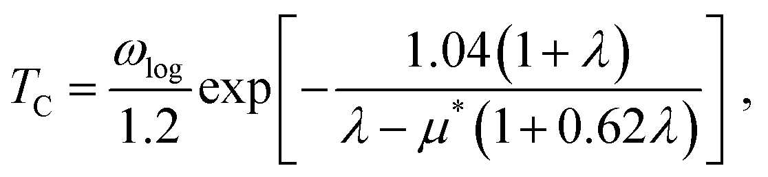 | (1) |
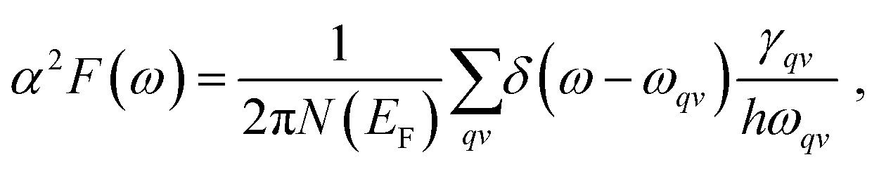 | (2) |
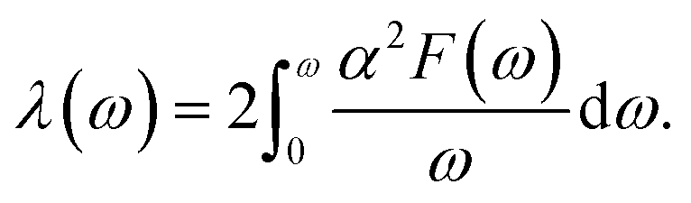 | (3) |
Experimental details
Experimentally, a suspension of titania nanosheets (Ti0.91O2) was prepared according to previous reports by Sasaki's group.39–42 In a typical synthesis process, the layered Cs0.68Ti1.83O4 precursor was obtained by a solid-state reaction, followed by proton-exchange to H0.68Ti1.83O4·H2O in hydrochloric acid and a delamination step in the presence of tetrabutylammonium cations (TBA+). The concentration of the Ti0.91O2 nanosheet suspension is ca. 1.79 g L−1. Atomic-scale observations were performed using an aberration-corrected scanning-transmission electron microscope (STEM), Nion UltraSTEM 100, operating at 60 kV. A detector half-angle range of 86–200 mrad was used to record high-angle annular dark-field images. Electron energy loss spectra (EELS) were collected using a Gatan Enfina spectrometer, with an energy resolution of ∼0.6 eV at 0.3 eV per channel energy dispersion. The convergence semi-angle of the incident electron probe was ∼30 mrad, and the collection semi-angle of EELS collection was ∼48 mrad. A power law was fitted for the background of the EELS spectra.3. Results and discussions
3.1. Experimental discovery of the Ti layer
In our experimental investigation, an aberration-corrected STEM machine operating at 60 kV was employed to manipulate this material. Interestingly, after ∼5 min irradiation, as revealed in Fig. 1(c), the O, K edge is largely diminished and has almost disappeared. In a comparison between the two EELS plots, only the Ti signature and no oxygen signatures are found, confirming that the nanosheets or small clusters on the surface are almost entirely made of Ti. This characterization indicates that the Ti0.91O2 nanosheet suspension is transforming to a Ti nanosheet under electron-beam irradiation. We subsequently construct the atomic structure of the Ti layer which, as the inset shows, agrees well with the observed image.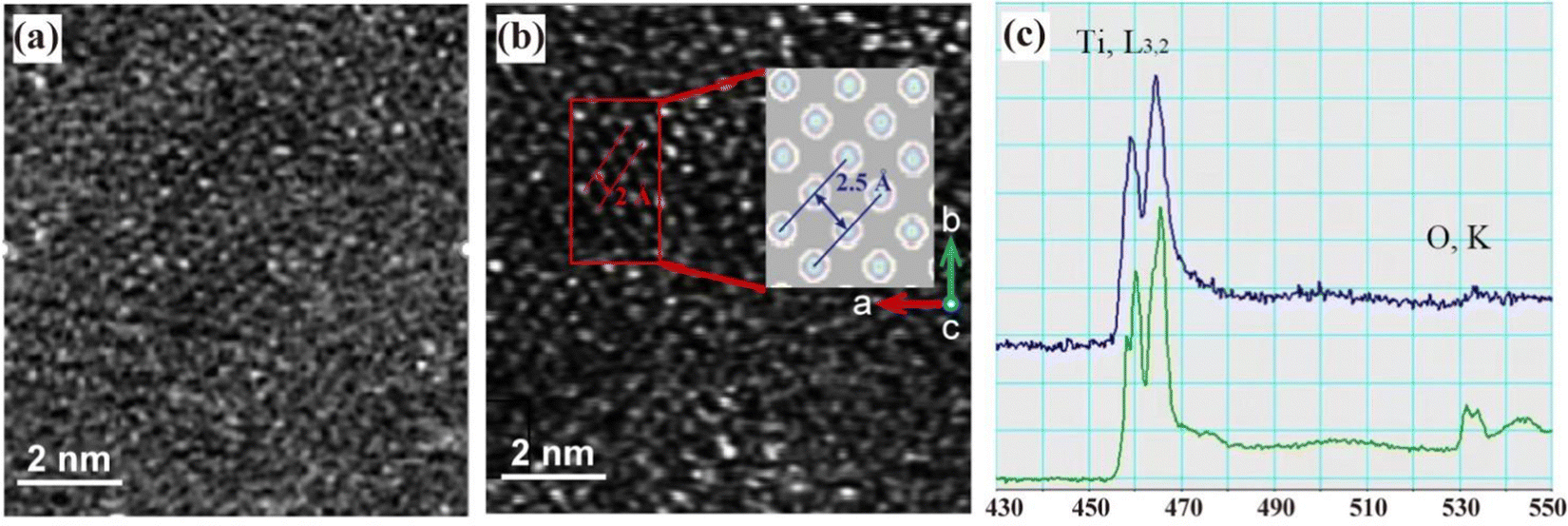 | ||
| Fig. 1 (a) STEM image of the unirradiated suspended sample. (b) STEM image of the irradiated suspended sample. The inset shows the atomic configuration after irradiation. (c) The electron energy loss spectrum (EELS) before (in green) and after (in blue) e-beam irradiation. The highlighted Ti, L3,2 and O, K edges are marked in the plot. | ||
It is known that image spots for bulk crystalline materials will be elongated along a certain direction, if the sample is tilted slightly off-zone. We observed the sample after tilting it by several degrees. It was noticed that all image spots are still round, instead of being elongated along a certain direction like the cases in bulk crystalline samples, as shown in Fig. S1 (ESI†). Therefore, the monolayer nature of the reported Ti monolayer can be confirmed. This figure is also added in ESI† Fig. S1, as ESI† describing the newly found Ti layer.
3.2. Towards the ground state in theory
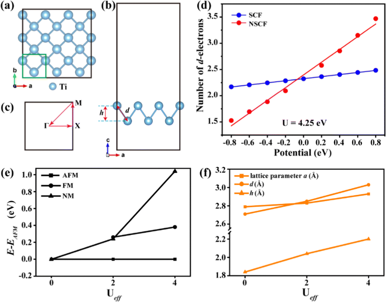 | ||
| Fig. 2 Crystal structures of the Ti monolayer: (a) top view, (b) side view, (c) the Brillouin zone of the monolayer with high-symmetry points. The unit cell is represented by the black rectangle. (d) The dependence of the linear response of d orbital occupation on potential shift. The blue and red lines indicate the interacting and bare response function χ and χ0. (e) The calculated energies of AFM, FM, and NM states and (f) the structural variances obtained with varying Ueff values. | ||
As discussed above, the d-electron monolayer might need a more sophisticated description, which is beyond DFT methods, because of the d orbital. In terms of the strong on-site orbital correlation strength, one can take an empirical value of Ueff = 2 eV. While the structural variance of this work compared with known types of Ti, Zr and Hf monolayers would lead to a different strength of correlation effects. Here, the linear response approach is applied to rationally estimate Ueff. As shown in Fig. 2(d), the calculated Ueff value for the Ti monolayer turns out to be 4.25 eV. Within the parameter in DFT+U, spin-polarization effects including the non-magnetic (NM), antiferromagnetic (AFM) and ferromagnetic (FM) configurations are considered. In addition, the AFM configurations can be expanded, and we have considered three AFM orders in this paper, as shown in Fig. S2 (ESI†), where the most favorable order is AFM1. For the magnetic properties, we thus adopt this configuration for further investigation. Fig. 2(e) also shows the calculated ‘Ueff–E’ relationship in the different magnetic orders, suggesting that the new Ti monolayer in both Ueff would be grounded to the AFM state. Interestingly, when U = 0 eV, the Ti monolayer falls into the NM state. In detail, Fig. 2(f) plots the calculated lattice parameters a, the Ti–Ti bond length d, and the thickness of the monolayer h at different Ueff values. It can clearly be observed in the figure that these three variables show an increasing trend with an increase in U from 0 to 4 eV. In addition, the Ti–Ti bond length d, the thickness of the monolayer h in different Ueff values can be found in Fig. 2(f). It can be observed that these three variables show an increasing trend with an increase in U from 0 to 4 eV.
To land on the true ground state of this new 2D layer, we are about to investigate the dynamical stabilities w/o Hubbard U corrections. As shown in Fig. 3, a series of phonon dispersion spectra is presented. It is clear that the six vibrational modes for each case are due to a unit cell composed of two atoms. Firstly, as shown in Fig. 3(a–b), Ueff equals either 2 or 4 eV, and the calculated phonon spectra of the AFM state always contains several imaginary modes. One can come to the conclusion that the Hubbard U correction would lead to non-negligible dynamic instability, so that we can rule out AFM from the candidate ground states. In addition, to confirm the instability of the case with U = 2 eV, a larger supercell of 6 × 6 × 1 is applied, and the calculated phonon dispersion curves can be found in Fig. S3 (ESI†). Notably, in plain DFT, the phonon dispersion curves of the Ti monolayer do not contain any imaginary modes, as shown in Fig. 3(c), indicating its dynamic stability. With regard to structural stability in the case of U = 2, we also undertake additional ab initio molecular dynamics (AIMD) simulation calculations by using a 5 × 5 × 1 supercell at 300 K with a time step of 2 fs with an accumulated time of 10 ps, as shown in Fig. S4 (ESI†). The free energy curves collected in AIMD demonstrate that in the case of U = 0 eV, the free energy curve is damped in a similar manner, over which no obvious structural reconstructions are noticed. Whereas in the case of DFT+U (U = 2 eV), after 6000 steps, the variance in the free energies begins to experience stronger oscillation, suggesting the structure is in transition or is undergoing strong perturbations. The averaged structure gives a more direct clue to the instability of the structure, as the inset shows. In summary, the dynamic stability and thermal stability demonstrate that the ground state of the novel Ti monolayer is the NM state, obtained in the plain DFT approach, and we thus take the NM state obtained as the ground state to conduct deeper and more extensive studies.
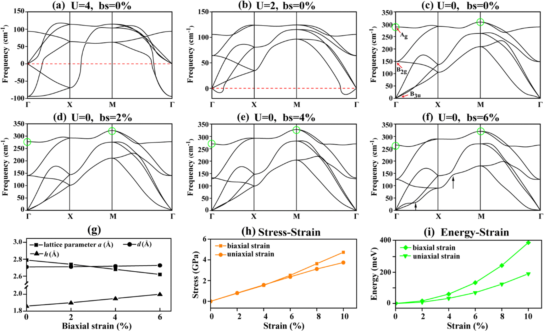 | ||
| Fig. 3 Phonon dispersion curves: (a) U = 4 eV, bs = 0%, (b) U = 2 eV, bs = 0%, (c) U = 0 eV, bs = 0%, (d) U = 0 eV, bs = 2%, (e) U = 0 eV, bs = 4%, and (f) U = 0 eV, bs = 6%. The main points of variance occurring in the vibrational spectra are marked by green circles. (g) The calculated in-plane lattice parameters a, bond lengths d, and thickness h under different biaxial strains. The calculated (h) stress–strain and (i) energy–strain relationships under biaxial and uniaxial strains. | ||
One may be curious about the strain effect on the vibrations. The phonon dispersion curves of the Ti monolayer under varying strains, i.e. bs = 2%, 4%, and 6%, in all cases remain dynamically stable, as displayed in Fig. 3(c–f). It is believed that the Ti monolayer still remains dynamically stable even under compressive strain. As to the origin of the vibrations, we consider the irreducible representation of the Ti monolayer at the Γ point, which can be denoted as follows: Γ = Ag + B2g + B3u, as shown in Fig. 3(c), where the Ag and B2g modes are both Raman active. For the three acoustic modes, the vibrational boundary can often reach 100 cm−1 without considerable changes. In the case of biaxial strain, the Ag mode experiences a visible reduction from 288.82 cm−1 to 264.69 cm−1 marked by the green circles. One can also see that when the strain is extended to 6%, the TA acoustic branch experiences an evident softening. In addition, strain-driven softening can also be found on the path between Γ and X, both marked by arrows in Fig. 3(f). In contrast, the global vibrational maximum situated at point M point is enhanced, implying that the Ti–Ti interaction shows an anisotropic characteristic. Overall, vibrational softening under compressive strain shows anisotropic behavior, which shows potential in shock-resistance applications.
Following the phonon spectra, we present the role of strain on the structure. Fig. 3(g) shows the calculated lattice parameters a, the length d of the Ti–Ti bond, and the thickness h of Ti–Ti layers under biaxial strains of varying magnitude. The thickness h (the out-of-plane direction) is the most responsive quantity to strain, confirming its anisotropic characteristics. Moreover, the measured Ti–Ti projection length in Fig. 1(b) is ∼2.5 Å, which is quite close to our calculated value of 2.0 Å, by considering the strain effect induced by the defects and more probably the rotation of the sample holder during the process of observation. This clearly suggests that good agreement between theory and experiment can be achieved.
We further use the stress–strain relation for the Ti monolayer, as shown in Fig. 3(h), to discuss the mechanical response to the biaxial and the uniaxial strain. The stress increases linearly with strain. Note that the initial slope of the stress–strain curves refers to the Young's modulus of 2D materials. The slopes under both biaxial and uniaxial strains are almost identical, suggesting that the Young's moduli of the Ti monolayer are extremely close to each other. In other words, the resistance to the deformation is almost identical. By fitting the stress–strain curves, we could obtain a Young's modulus of about 70.8 N m−1. When further strain is imposed, the stress–strain curves of the biaxial strain begin to diverge and to show a nonlinear trend.
Apart from the Young's modulus, we also calculate the elastic stiffness constants. For the 2D orthogonal lattice, only four independent elastic stiffness constants (C11, C22, C12 and C66) need to be considered. C11 (C22) and C12 refer to the stiffness response to the uniaxial strains along the x (y) directions and the biaxial strain, respectively. The elastic stiffness constants C11 and C22 are almost identical due to in-plane equivalency, and both are about 76 N m−1. The remaining two moduli, C12 and C66, are relatively low at only 2.5 and 4.3 N m−1. Here, the calculated Young's modulus based on Cij is 75.9 N m−1, in very good agreement with the fitted value of 70.8 N m−1. The energy–strain curves are also displayed in Fig. 3(i) corresponding to the total energy difference between the strained and unstrained systems. It can be seen that the energy starts to diverge at the onset of the applied strain and shows an exponential tendency in the regime of larger strain. The Young's modulus should be around 71 N m−1, which is very close to C11/C22. Compared to some of the elemental monolayers, the phosphorene series has moduli of about 21.9–56.3 N m−1, much lower than for our proposed new Ti monolayer.43 Even for some recently found MnSi and MnC0.5Si0.5 layers, the Young's moduli reach 9.53 N m−1 and 24.3 N m−1.44 We can therefore conclude that the newly established Ti monolayer is elastically stable and capable of withstanding an external strain.
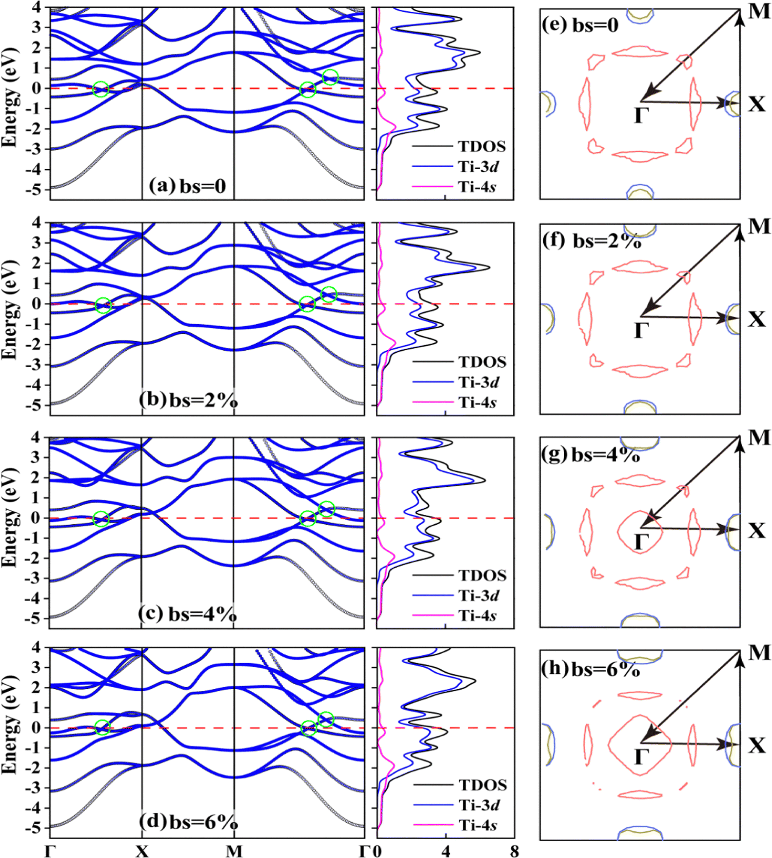 | ||
| Fig. 4 (a–d) band structures (left), the projected and total density of states (DOS) (middle), and (e and f) the Fermi surface under different biaxial strains (bs): 0, 2%, 4%, and 6%. The bands crossing the Fermi energy are colored differently. The Ti-3d and Ti-4s orbital projected DOS and total DOS are colored in blue, pink and black. The evolution of the Dirac points is marked by green circles. | ||
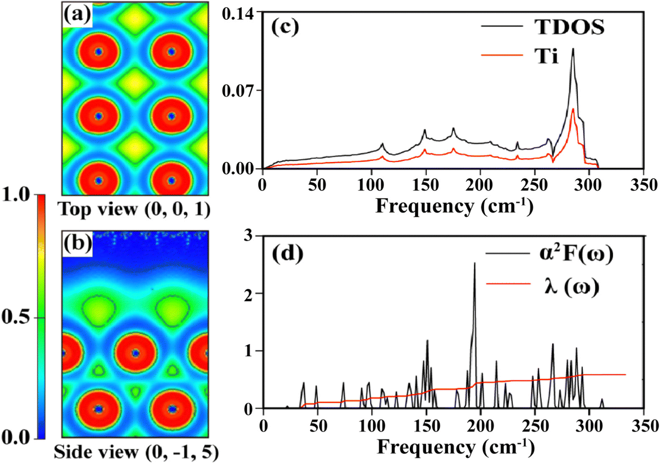 | ||
Fig. 5 The electron localization function (ELF) in planes of (a) (001) and (b) (0![[1 with combining macron]](https://www.rsc.org/images/entities/char_0031_0304.gif) 5). The colored bar stands for the degree of electron localization. (c) The atomic resolved and total phonon density of states (PHDOS) are in red and blue colors. (d) The Eliashberg spectral function α2F(ω) and the electron–phonon coupling constant λ(ω). 5). The colored bar stands for the degree of electron localization. (c) The atomic resolved and total phonon density of states (PHDOS) are in red and blue colors. (d) The Eliashberg spectral function α2F(ω) and the electron–phonon coupling constant λ(ω). | ||
It is worth noting that throughout the strained cases, the Ti monolayer retains metallicity, as shown in Fig. 4(b–d). The physical phenomena related to the electronic structure of the strained Ti monolayer are similar to the unstrained case; thus we do not make redundant reports. But, interestingly, three Dirac points near the vicinity of the Fermi energy are found in this system, marked by the green circles in Fig. 4(a). If we concentrate only on the Fermi energy regime, the three Dirac points identified here are located at ∼−0.05 eV along Γ–X and at ∼−0.1 eV and 0.38 eV along M–Γ. (see details in Fig. S6(a–c), ESI†). Specifically, the first two points at or near the Fermi energy show slopes of −6.34 and 9.39 eV Å−1 along Γ–X, and −4.18 and 15.69 eV Å−1 along M–Γ. Only at the third point is a parabolic characteristic more evident. By proceeding to orbital decomposition, one can see that the other four non-dxy orbitals contribute to the Fermi energy, and it is the dxz and dyz orbitals that contribute to the other two Dirac points, as suggested by Fig. S7 (ESI†). It is noteworthy that all three points show Dirac-type characteristics with linear dispersion, which may make a large contribution to electrical transport.
On the right of the bands, the corresponding Fermi surfaces (FSs) are plotted in Fig. 4(e–h). It is found that the FS is almost all contributed by the bands along M–Γ and composed of a total of three bands passing through the Fermi energy. Near the zone center, four larger and four smaller semi-triangles form a square, as the red sheets show. Interestingly, all these triangles point outward, when free of strain. Whereas under strain, the originally larger triangles are enlarged at the beginning and squeezed subsequently, along with a simultaneous diminishment of their counterparts. The two semi-spherical FS sheets near M contributed by the blue- and orange-colored bands shown in Fig. S7 (ESI†), are also expanded by imposing larger strains. One of the most striking changes occurring in FS lies in the onset of the interior quadrangles, when bs reaches 4% and more, as shown in Fig. 4(g–h). Such a change in FS clearly brings about an electronic topological transition (ETT).48,49 It is emphasized that approximately in the middle of X–Γ, the smaller FS sheets in the corners almost disappear, allowing for another occurrence of ETT. A band structure and FS with an expanded k-path have been added, as shown in Fig. S8 (ESI†) to draw a full picture of the electronic states. These tunable FS and band-dependent responses to an external stimulus might lead to anomalous conduction behavior and the possibility of being used as strain-based sensors.
3.3. Electron–phonon coupling and superconductivity
For the new Ti layer, ELF plots on two planes of (001) and (05) are provided to understand the bonding characteristics. The former is the ELF on the top view, and the latter is the best representative of T–Ti bonding, as shown in Fig. 5(a and b). The red regime shows that the electrons are highly localized (1 for full localization) and vice versa for the blue regime, as visible in the color bar. The Ti–Ti interatomic ELF mostly reaches about 0.5–0.8 electrons per Bohr3, which is neither localized nor very delocalized. Such results reveal that the Ti monolayer is dominated by metallic bonding. One can also observe that the surface of the monolayer has a lot of electron cloud, implying a chemically active characteristic.
As suggested by the ETT and electronic structure, the possibility of being a superconductor does exist.50 Here, we applied an electron–phonon coupling based mechanism, in a simplified Bardeen–Cooper–Schrieffer (BCS) theory, to investigate its superconducting possibility. For the transition metal series, it is recognized that it is primarily the d electrons near the Fermi energy that participate in the Bardeen–Cooper–Schrieffer (BCS) condensation process at Tc. The BCS theory demonstrates that the transition to the superconducting state is caused by the pairing of itinerant electrons mediated by their vibrations in metals.51 It is the interaction between the itinerant conduction electrons and phonons that overcomes the natural repulsive interactions between electrons to form Cooper pairs, which then subsequently condense at Tc into the superconducting state.52 Thereby, the Eliashberg spectral function α2F(ω) and the (electron–phonon coupling) EPC constant λ are presented in Fig. 5(d). At a lower frequency up to 157 cm−1, the Eliashberg spectral function exhibits several peaks, leading to a steady increase in EPC, accounting for 55% of the total EPC (λ = ![[thin space (1/6-em)]](https://www.rsc.org/images/entities/char_2009.gif) 0.58). Going through a phonic gap above 157 cm−1, the highest peak of α2F(ω) is present at 196 cm−1, ahead of more discrete peaks at higher frequencies. The phonon modes between 192 and 300 cm−1 provide 45% contributions to the total EPC, showing that λ(ω) experiences a steady increase in this region of frequencies. The increase in Tc can be traced back to the fact that there are interactions between the dual Ti atoms, particularly for the frequency regime above 180 cm−1. In the phonon DOS plot of Fig. 5(c), locations of peaks and α2F(ω) are in good agreement, which is decisive for the behavior of λqν. According to Ref. 38 this newly established Ti monolayer is a medium-coupling superconductor with a λ of 0.58 with a Tc of 3.8 K. This provides clues for us to design 2D superconducting systems with pure d metal elements and opens the road toward fabricating stable, robust, and high-performance 2D superconductors.
0.58). Going through a phonic gap above 157 cm−1, the highest peak of α2F(ω) is present at 196 cm−1, ahead of more discrete peaks at higher frequencies. The phonon modes between 192 and 300 cm−1 provide 45% contributions to the total EPC, showing that λ(ω) experiences a steady increase in this region of frequencies. The increase in Tc can be traced back to the fact that there are interactions between the dual Ti atoms, particularly for the frequency regime above 180 cm−1. In the phonon DOS plot of Fig. 5(c), locations of peaks and α2F(ω) are in good agreement, which is decisive for the behavior of λqν. According to Ref. 38 this newly established Ti monolayer is a medium-coupling superconductor with a λ of 0.58 with a Tc of 3.8 K. This provides clues for us to design 2D superconducting systems with pure d metal elements and opens the road toward fabricating stable, robust, and high-performance 2D superconductors.
4. Conclusions
In summary, we use electron-beam irradiation to manufacture a new 2D Ti nanosheet from a suspension of Ti0.91O2 nanosheets. Based on first-principles calculation, the newly found Ti monolayers fall into metallic nature and are elastically and dynamically stable, even withstanding a strain up to 6%. The Young's modulus is calculated to be 70.8 N m−1 and shows excellent robustness. The electron–phonon coupling is at a medium level of about 0.58, in which phonon modes below 157 cm−1 and higher frequency phonons make roughly equivalent contributions. The estimated superconducting transition temperature is 3.8 K. This provides clues to the occurrence of superconductance on ultra-thin d-metal-based layers, offering more opportunities for manufacturing robust low-dimensional and low-cost electronic components. Under slight mechanical stimuli, ETTs take place along Γ–X and M–Γ, which are primarily mediated by the dz2 and dx2−y2 orbitals. Our findings will boost sustainable efforts at fabricating novel d metal 2D layers as components of superior quantum and electronic devices.Conflicts of interest
There are no conflicts to declare.Acknowledgements
W. S. acknowledges the National Natural Science Foundation of China (No. 51902052) and the Jiangsu Shuangchuang (Mass Innovation and Entrepreneurship) Talent Program (JSSCBS20210109). L. S. acknowledges the National Natural Science Foundation of China (No. 12234005), the key research and development program of Jiangsu Province (BE2021007-2). W. S., J. Z. and L. S. are partially supported by “the Fundamental Research Funds for the Central Universities”. Z. Y. is supported by Guangdong Province (2021B0301030003). We also thank the Big Data Computing Center of Southeast University for providing the facility support on the numerical calculations in this paper.References
- A. K. Geim and K. S. Novoselov, Nat. Mater., 2007, 6(3), 183–191 CrossRef CAS PubMed.
- K. S. Novoselov, A. K. Geim and S. V. Morozov, et al. , Science, 2004, 306(5696), 666–669 CrossRef CAS PubMed.
- J. Zhou, J. Lin and X. Huang, et al. , Nature, 2018, 556(7701), 355–359 CrossRef CAS PubMed.
- H. Okamoto, Y. Kumai and Y. Sugiyama, et al. , J. Am. Chem. Soc., 2010, 132(8), 2710–2718 CrossRef CAS PubMed.
- M. Corso, W. Auwärter and M. Muntwiler, et al. , Science, 2004, 303(5655), 217–220 CrossRef CAS PubMed.
- Q. Tang, Y. Li and Z. Zhou, et al. , ACS Appl. Mater. Interfaces, 2010, 2(8), 2442–2447 CrossRef CAS PubMed.
- B. Radisavljevic, A. Radenovic and J. Brivio, et al. , Nat. Nanotechnol., 2011, 6(3), 147–150 CrossRef CAS PubMed.
- D. C. Elias, R. R. Nair and T. Mohiuddin, et al. , Science, 2009, 323(5914), 610–613 CrossRef CAS PubMed.
- Y. Wang, L. Deng and Q. Wei, et al. , Nano Lett., 2020, 20(3), 2129–2136 CrossRef CAS PubMed.
- X. Zhao, D. Fu and Z. Ding, et al. , Nano Lett., 2018, 18(1), 482–490 CrossRef CAS PubMed.
- K. S. Novoselov, A. K. Geim and S. V. Morozov, et al. , Nature, 2005, 438(7065), 197–200 CrossRef CAS PubMed.
- L. Li, Y. Wang and S. Xie, et al. , Nano Lett., 2013, 13(10), 4671–4674 CrossRef CAS PubMed.
- X. Li, Y. Dai and Y. Ma, et al. , Phys. Chem. Chem. Phys., 2014, 16(26), 13383–13389 RSC.
- D. Voiry, A. Mohite and M. Chhowalla, Chem. Soc. Rev., 2015, 44(9), 2702–2712 RSC.
- J. Wang, Y. Wei and H. Li, et al. , Sci. China: Chem., 2018, 61(10), 1227–1242 CrossRef CAS.
- Y. Xiao, M. Zhou and J. Liu, et al. , Sci. China Mater., 2019, 62(6), 759–775 CrossRef CAS.
- X. Wang, Z. Song and W. Wen, et al. , Adv. Mater., 2019, 31(45), 1804682 CrossRef CAS PubMed.
- M. S. Sokolikova and C. Mattevi, Chem. Soc. Rev., 2020, 49(12), 3952–3980 RSC.
- H. Bergeron, D. Lebedev and M. C. Hersam, Chem. Rev., 2021, 121(4), 2713–2775 CrossRef CAS PubMed.
- B. Zhou, S. Dong and X. Wang, et al. , Appl. Surf. Sci., 2017, 419, 484–496 CrossRef CAS.
- A. Hashmi, M. Umar Farooq and I. Khan, et al. , Nanoscale, 2017, 9(28), 10038–10043 RSC.
- X. Zhao, K. P. Loh and S. J. Pennycook, J. Phys.: Condens. Matter, 2020, 33(6), 063001 CrossRef PubMed.
- S. Kim, S. Jung and J. Lee, et al. , ACS Appl. Mater. Interfaces, 2020, 12(35), 39595–39601 CrossRef CAS PubMed.
- S. Kim and A. G. Fedorov, FEBIP for functional nanolithography of 2D nanomaterials, Georgia Institute of Technology, Atlanta, GA (United States), 2020 Search PubMed.
- X. Zhao, J. Dan and J. Chen, et al. , Adv. Mater., 2018, 30(23), 1707281 CrossRef PubMed.
- D. Qiu, C. Gong and S. Wang, et al. , Adv. Mater., 2021, 33(18), 2006124 CrossRef CAS PubMed.
- R. Lorenz and J. Hafner, Phys. Rev. B: Condens. Matter Mater. Phys., 1996, 54(22), 15937–15949 CrossRef CAS PubMed.
- J. Zhao, Q. Deng and A. Bachmatiuk, et al. , Science, 2014, 343(6176), 1228–1232 CrossRef CAS PubMed.
- D. Vanderbilt, Phys. Rev. B: Condens. Matter Mater. Phys., 1990, 41(11), 7892–7895 CrossRef PubMed.
- K. Laasonen, A. Pasquarello and R. Car, et al. , Phys. Rev. B: Condens. Matter Mater. Phys., 1993, 47(16), 10142–10153 CrossRef CAS PubMed.
- K. Lejaeghere, G. Bihlmayer and T. Björkman, et al. , Science, 2016, 351(6280), aad3000 CrossRef PubMed.
- G. Prandini, A. Marrazzo and I. E. Castelli, et al. , npj Comput. Mater., 2018, 4(1), 72 CrossRef.
- S. Baroni, S. de Gironcoli and A. Dal Corso, et al. , Rev. Mod. Phys., 2001, 73(2), 515–562 CrossRef CAS.
- P. Miró, M. Audiffred and T. Heine, Chem. Soc. Rev., 2014, 43(18), 6537–6554 RSC.
- M. Cococcioni and S. de Gironcoli, Phys. Rev. B: Condens. Matter Mater. Phys., 2005, 71(3), 035105 CrossRef.
- A. Togo, F. Oba and I. Tanaka, Phys. Rev. B: Condens. Matter Mater. Phys., 2008, 78(13), 134106 CrossRef.
- P. B. Allen, Phys. Rev. B: Solid State, 1972, 6(7), 2577–2579 CrossRef CAS.
- P. B. Allen and R. C. Dynes, Phys. Rev. B: Solid State, 1975, 12(3), 905–922 CrossRef CAS.
- T. Sasaki, M. Watanabe and H. Hashizume, et al. , J. Am. Chem. Soc., 1996, 118(35), 8329–8335 CrossRef CAS.
- T. Sasaki and M. Watanabe, J. Am. Chem. Soc., 1998, 120(19), 4682–4689 CrossRef CAS.
- T. Sasaki, Y. Ebina and Y. Kitami, et al. , J. Phys. Chem. B, 2001, 105(26), 6116–6121 CrossRef CAS.
- T. Sasaki and M. Watanabe, J. Phys. Chem. B, 1997, 101(49), 10159–10161 CrossRef CAS.
- J. Jiang and H. S. Park, J. Phys. D: Appl. Phys., 2014, 47(38), 385304 CrossRef.
- B. Zhang, G. Song and J. Sun, et al. , Nanoscale, 2020, 12(23), 12490–12496 RSC.
- J. Heyd, G. E. Scuseria and M. Ernzerhof, J. Chem. Phys., 2003, 118(18), 8207–8215 CrossRef CAS.
- B. Silvi and A. Savin, Nature, 1994, 371(6499), 683–686 CrossRef CAS.
- K. Koumpouras and J. A. Larsson, J. Phys.: Condens. Matter, 2020, 32(31), 315502 CrossRef CAS PubMed.
- W. Sun, S. Chakraborty and R. Ahuja, Appl. Phys. Lett., 2013, 103, 251901 CrossRef.
- W. Sun, W. Luo and Q. Feng, et al. , Phys. Rev. B, 2017, 95(11), 115130 CrossRef.
- C. Ji, B. Li and W. Liu, et al. , Nature, 2019, 573(7775), 558–562 CrossRef CAS PubMed.
- J. Bardeen, L. N. Cooper and J. R. Schrieffer, Phys. Rev., 1957, 108(5), 1175–1204 CrossRef CAS.
- H. Fröhlich, Phys. Rev., 1950, 79(5), 845–856 CrossRef.
Footnotes |
| † Electronic supplementary information (ESI) available. See DOI: https://doi.org/10.1039/d2nh00508e |
| ‡ X. Z. and J. T. are equivalent contributors. |
| This journal is © The Royal Society of Chemistry 2023 |