
 Open Access Article
 This Open Access Article is licensed under a Creative Commons Attribution-Non Commercial 3.0 Unported Licence
Hyperspectral mapping of nanoscale photophysics and degradation processes in hybrid perovskite at the single grain level†
Ethan J.
Taylor
a,
Vasudevan
Iyer
b,
Bibek S.
Dhami
a,
Clay
Klein
c,
Benjamin J.
Lawrie
 *bd and
Kannatassen
Appavoo
*a
*bd and
Kannatassen
Appavoo
*a
aDepartment of Physics, University of Alabama at Birmingham, 1300 University Blvd., Birmingham AL, 35294 USA. E-mail: appavoo@uab.edu
bCenter for Nanophase Materials Sciences, Oak Ridge National Laboratory, Oak Ridge, TN 37831, USA. E-mail: lawriebj@ornl.gov
cClarion University, 840 Wood St, Clarion, PA 16214, USA
dMaterials Science and Technology Division, Oak Ridge National Laboratory, Oak Ridge, TN 37831, USA
First published on 24th August 2023
Abstract
With solar cells reaching 26.1% certified efficiency, hybrid perovskites are now the most efficient thin film photovoltaic material. Though substantial effort has focussed on synthesis approaches and device architectures to further improve perovskite-based solar cells, more work is needed to correlate physical properties of the underlying film structure with device performance. Here, using cathodoluminescence microscopy coupled with unsupervised machine learning, we quantify how nanoscale heterogeneity globally builds up within a large morphological grain of hybrid perovskite when exposed to extrinsic stimuli such as charge accumulation from electron beams or milder environmental factors like humidity. The converged electron-beam excitation allows us to map PbI2 and the emergence of other intermediate phases with high spatial and energy resolution. In contrast with recent reports of hybrid perovskite cathodoluminescence, we observe no significant change in the PbI2 signatures, even after high-energy electron beam excitation. In fact, we can exploit the stable PbI2 signatures to quantitatively map how hybrid perovskites degrade. Moreover, we show how our methodology allows disentangling of the photophysics associated with photon recycling and band-edge emission with sub-micron resolution using a fundamental understanding of electron interactions in hybrid perovskites.
Introduction
Over the last decade, hybrid organic-inorganic perovskites (hybrid perovskites) have generated widespread interest for applications in photovoltaics,1–6 light-emitting diodes,7–9 sensing,10–12 and neuromorphic computing.13,14 This interest is a result of their impressive electronic properties, such as a high absorption coefficient, tunable optoelectronic properties via synthesis, and long carrier lifetimes and diffusion lengths. However, the stability of hybrid perovskite remains an obstacle for future applications. A deeper understanding of nanoscale heterogeneity and how it affects long-term stability and phase stabilization is critically needed. Recent studies have shown that understanding film morphology and controlling intra-grain structure15 may enable optimized charge carrier dynamics for specific device requirements.16,17 However, the exact role played by grain boundaries, beneficial18,19 or detrimental,20,21 is still under debate.Various microscopy and spectroscopy techniques have been employed to quantify the effect of grain structure and morphology on charge carrier dynamics and transport. For example, transmission electron microscopy (TEM) has been used to characterize how lead-related defects are formed and how they are localized at boundaries.22 TEM has also been used to characterize temperature-dependent phase transitions, e.g., from tetragonal MAPbI3 to trigonal PbI2.23 Other recent work has pointed towards humidity as a driving factor in how grain boundaries influence phase separation and film degradation.24 Spectroscopic tools like confocal microscopy have also been employed to map excited-state energetics and dynamics in grain interiors and grain boundaries through intensity and lifetime measurements,25–27 providing insights into the effect of grain boundaries on the optoelectronic properties of hybrid perovskite thin films.27–33
Beyond the optical diffraction limit, cathodoluminescence (CL) microscopy has emerged as a powerful tool for mapping the optical properties of hybrid perovskites at the nanoscale. The electron beam can locally excite and probe the optoelectronic properties of hybrid perovskites, provided that optimal electron beam energy and detector acquisition times are selected.34 As shown recently,35 excessive electron beam doses can locally heat the hybrid perovskite films, leading to phase separation and film decomposition. For example, in the case of prototypical CH3NH3PbI3, exposure to high electron beam energies (>10 kV) was reported to increase PbI2 emission and create an intermediate phase with emission that is blue-shifted from the primary band-edge emission (∼760 nm), which has been attributed to beam degradation and local heating.34,35 These experiments provided initial evidence that the electron beam probe can be used to characterize the performance and stability of hybrid perovskite devices as long as the damage mechanism triggered by the electron beam is well understood.
In this work, we employ CL microscopy to collect hyperspectral datasets and use unsupervised machine-learning techniques to generate maps that quantify photophysical properties of a hybrid perovskite thin film of CH3NH3PbI3 at the single grain level. We probe the nanoscale energetics of the grain interior and at its boundaries as a function of increasing electron beam energies or exposure to an environmental stimuli (e.g., humidity). To obtain these correlated maps of grain morphology and associated photophysics, the raw hyperspectral datasets are analysed using non-negative matrix factorization (NMF) techniques, which autonomously generate spectrally-dependent maps. For example, our unsupervised analysis highlights that humidity-based degradation, as revealed by the presence of PbI2 emission signatures, is mostly localized near grain boundaries and on the surface of the film. These results are supported by systematically increasing the energy of the electron beam to probe both depth-dependent photophysical effects and beam-induced damage. Importantly, the Gaussian-prior guided analysis shows that humidity based PbI2 damage of the hybrid perovskite does not vary with beam induced damage and remains localized to grain boundaries and surfaces. With knowledge of the damage signatures expected in this prototypical material, we proceed with unsupervised NMF techniques to spatially resolve other important photophysical processes like photon-recycling and band-edge emission as a function of excitation depth.
Experimental methods
Sample preparation
Hybrid organic–inorganic perovskites samples were prepared via a solution-processed technique, using a slight modification to the hot-casting method conducted by Nie et al.36,37 First, microscope cover glass substrates (25 mm × 25 mm, Fisher scientific) were cleaned using acetone (Sigma Aldrich, 99%). Zinc oxide nanospheres (ZnO, <130 nm, 40 wt% in ethanol, Sigma Aldrich) were spin coated on these glass substrates, then these coated glass coverslips are baked at 100 °C to evaporate the residual ethanol. These coated glass coverslips were used as substrate for the perovskite and the coating with the ZnO to ensure the uniform heating of the substrate. 0.578 g of lead iodide (PbI2, 99%) and 0.2 g of methyl ammonium iodide (CH3NH3I, 98%) were mixed in 1 ml of anhydrous N,N-dimethylformamide (DMF, 99%) in a glass vial. This perovskite precursor solution was heated to 120 °C while the substrate, as treated above, was heated to 300 °C. Then the heated substrate was transferred to the spin coater and the heated perovskite precursor solution was spin-coated at 5000 rpm for 5 seconds and transferred back to the heater (maintained at 300 °C) for 2 seconds. This approach produced a uniform hybrid perovskite thin film with large morphological grains, which are desired for application purposes. We note that while the majority of those grains extend to the substrate,36,37 they may not necessarily share the same crystallographic orientation. Recent studies using electron backscatter diffraction and photoemission electron microscopy have shown that local optoelectronic maps are more complex than previously thought, largely because of the multiple crystallographic sub-grains and the various defect types (e.g., PbI2, grain boundary and polytype) that exist.38–40 High-resolution SE micrographs of these morphologically large grains and the boundary among them are shown in ESI Fig. 1.† All samples that were fabricated for this study have thicknesses of around one micron.37 All the processes involved in this fabrication were carried out in a nitrogen filled glovebox. The chemicals were purchased from Sigma-Aldrich and were used without any further purification. The pristine thin films were then vacuum sealed in a nitrogen environment for comparison with environmentally exposed samples that were exposed to air.Cathodoluminescence microscopy
Cathodoluminescence microscopy is now a workhorse tool for characterizing nanophotonic materials. When a high-energy converged primary electron beam interacts with a sample, the transmitted, secondary, and backscattered electrons are routinely used to characterize the sample morphology. The primary electrons scatter within the investigated material and generate around 102 to 103 electron–hole pairs per incident electron that subsequently recombine via radiative and non-radiative processes.34 CL microscopy is often delineated into coherent and incoherent CL, depending on the nature of the emission process.41 Coherent CL, so named because the emitted photons have a defined phase relationship with the electron excitation, results from incident electrons polarizing material at interfaces; it is frequently used to probe the local density of states of nanophotonic and plasmonic media.42–45 Incoherent CL typically measures the spontaneous emission of excited states after the electron beam deposits energy in matter, and so is a powerful tool for measuring the energetics and dynamics of defects and excitons in heterogeneous nanoscale materials.20,34,35,46–50We probe the incoherent CL generated within a large grain of hybrid perovskite thin film using a FEI Quattro environmental SEM with a Delmic Sparc CL collection module that employs a parabolic mirror to collect the CL generated by the film following electron beam excitation. An electron beam with energy of 2–20 kV passes through a small hole in a parabolic mirror before exciting the sample with a spot size of order 1 nm. The parabolic mirror then collects the resulting emission and directs it through a focusing lens into an Andor Kymera spectrograph. An Everhart–Thornley detector is used to measure the secondary electron (SE) signal concurrently with the CL signal. The CL measurement in Fig. 1 was performed with a beam current of 110 pA, utilizing a 200 ms acquisition time per spectrum. The other grains presented in this work are analysed in the same way with slightly varying current values chosen to ensure the current remains low enough to prevent rapid beam-induced degradation but high enough to ensure a satisfactory signal-to-noise ratio with the desired spectral acquisition time.51 SEM images collected at 10 kV of accelerating voltage for the datasets in Fig. 2, 3, and 4 are presented in ESI Fig. 2.†
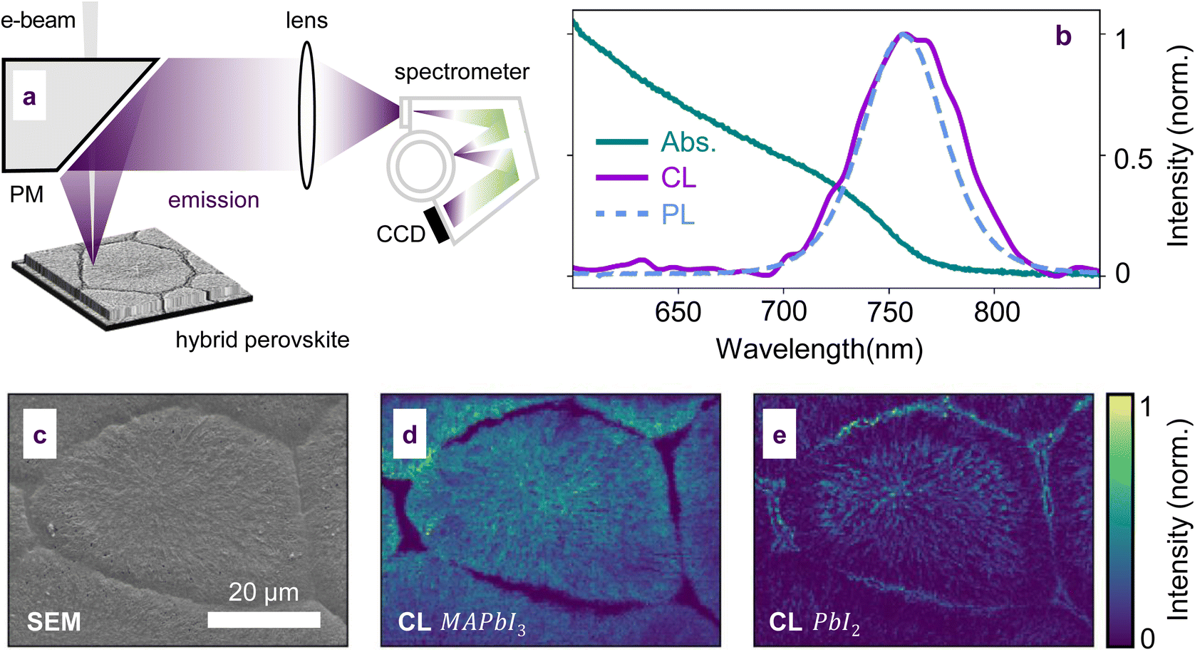 | ||
| Fig. 1 Overview of cathodoluminescence spectroscopy of large-grain hybrid perovskites. (a) Schematic of CL setup. The electron beam passes through a hole in a parabolic mirror before exciting the sample. The collimated cathodoluminescence is collected and characterized in a spectrometer mounted outside the chamber. (b) Representative spectra of optical absorption, photoluminescence and CL collected at the centre of a grain. (c) Scanning electron micrograph (SEM) of a grain imaged using a 5 kV beam energy with a horizontal field of view of 61 μm. Normalized single-wavelength CL intensity maps of the (d) hybrid perovskite band-edge (λ = 765 nm) and (e) PbI2 emission (λ = 510 nm). Same scale bar as (c). | ||
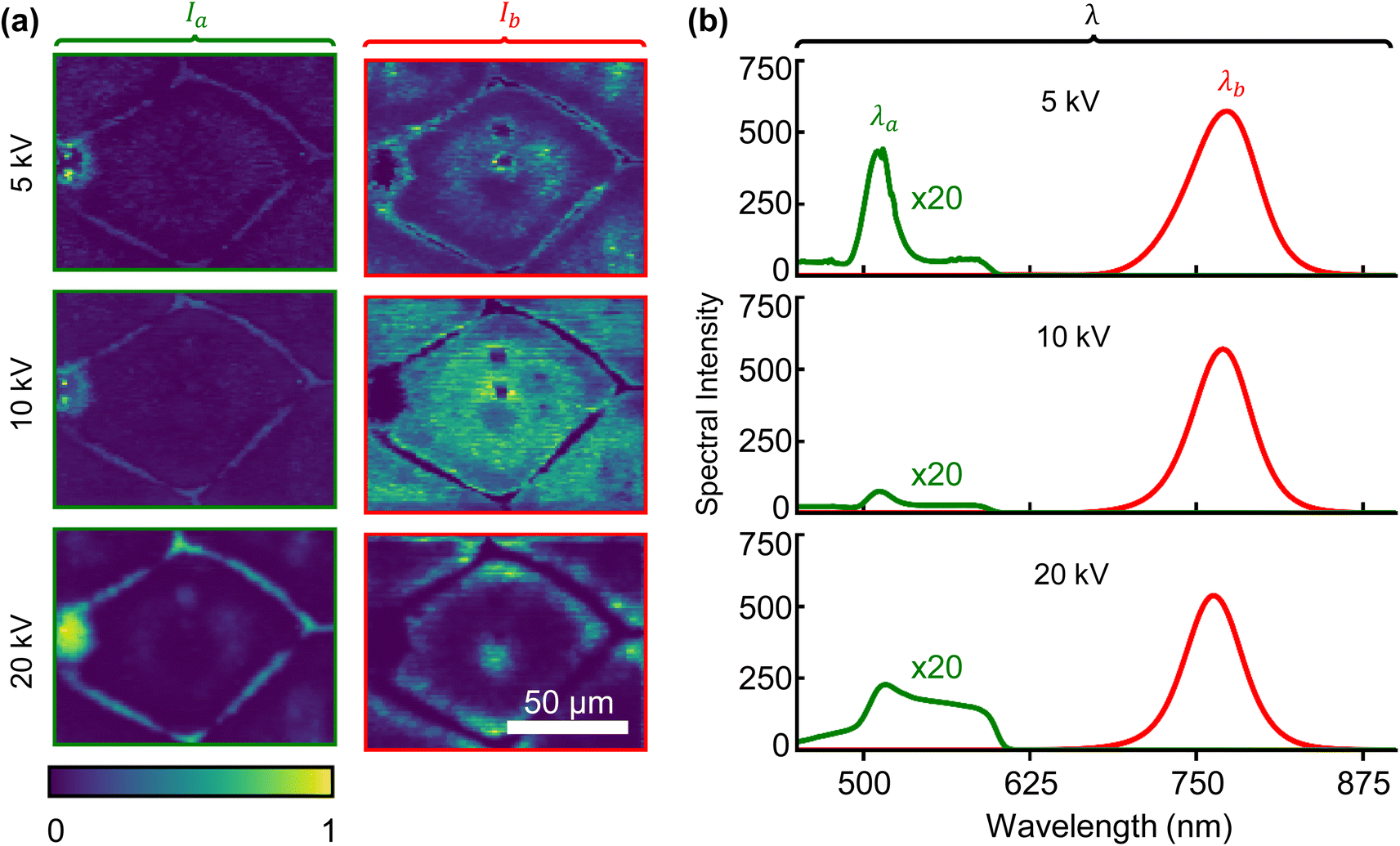 | ||
| Fig. 2 NMF decomposition showing accelerating voltage dependence on the cathodoluminescence of a hybrid perovskite grain. (a) Normalized spatial intensity maps resulting from the NMF decomposition corresponding to contributions from the PbI2 signal shown in Ia and the main hybrid perovskite emission shown in Ib. (b) Corresponding spectral vectors from the PbI2 signal (green) and the main perovskite (red). The magnitude of the spectral vectors have been scaled with respect to the raw experimental counts. Therefore, the matrix product of (a) and (b) reproduces each original CL hyperspectral dataset. Note that the PbI2 (λa) was scaled by a factor of 20 for visibility. | ||
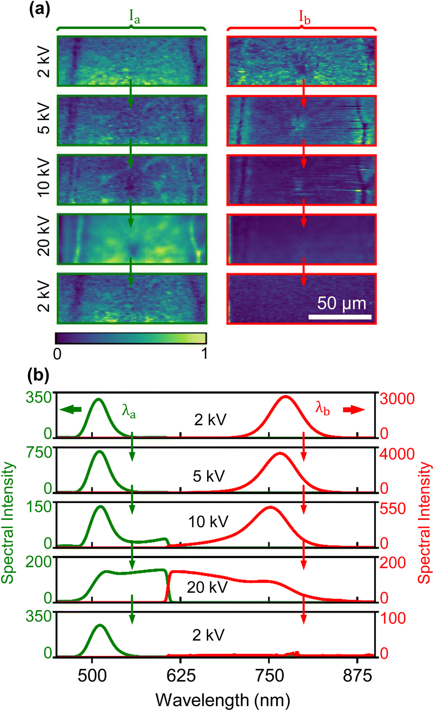 | ||
| Fig. 3 NMF decomposition of CL hyperspectral dataset of a grain exposed to environment. (a) Normalized NMF spatial intensity maps for an electron-beam energy sweep starting at 2 kV and ending at 2 kV, shown in the order of measurement as top to bottom, with colour corresponding to the spectral contributions shown in (b). Ia shows negligible beam-induced modification of the PbI2 signal between the initial and final 2 kV measurements, and Ib shows the degradation of the main perovskite emission phase due to beam damage. | ||
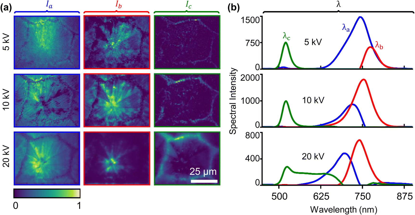 | ||
| Fig. 4 Blind NMF decomposition of environmentally exposed sample with rank three. (a) Normalized spatial intensity maps resulting from the NMF decomposition. Ia corresponds to primary band-edge recombination spatial locations, Ib corresponds to photon recycling, and Ic is the PbI2 CL. (b) The spectral vectors which pair to the spatial intensity maps in (a). As accelerating voltage is increased, the spectral shapes and spatial intensity maps change due to energy deposition depth and beam induced damage. | ||
Non-negative matrix factorization (NMF)
The collected CL hyperspectral datasets contain on the order of 100 × 100 × 1024 pixels (length × width × wavelength), and an appropriate analysis technique is needed to extract photophysics of interest from each hyperspectral dataset. NMF is a method of grouping and decomposing data through unsupervised learning.52–57 We decompose our hyperspectral CL dataset using NMF to obtain the component spectral vectors and their corresponding spatial intensity maps.58,59 The NMF decomposes the hyperspectral dataset X with n × m spatial pixels and spectrum of dimension α and approximates this hyperspectral dataset via the matrix product of the spectral vectors λ and the associated spatial intensity maps I,| X(n×m)×α ≈ I(n×m)×rλr×α |
All NMF decompositions were performed using the Nimfa Python package.60 Before the NMF algorithm was applied, the spectral data was cropped to the range of interest and denoising was done via wavelet denoising, a Savitzky–Golay filter, and a median filter. The average spectra obtained after this process for each of the datasets presented in Fig. 2, 3, and 4 are shown in ESI Fig. 2.† For the Gaussian-initialized NMF, which are shown in Fig. 2 and 3, a median filter was applied after decomposition to remove cosmic rays, which saturated isolated pixels. The effect of our median filter is shown in ESI Fig. 3 and 4.† The spectral vectors in all decompositions have been scaled by the raw emission counts. A full description of the NMF analysis of these CL images is presented in the ESI.†
Results and discussion
A schematic of the cathodoluminescence microscope used to collect the hyperspectral images is shown in Fig. 1(a). Normalized optical absorption, photoluminescence (PL) and CL from the centre of a grain are shown in Fig. 1(b), a secondary electron (SE) map of a prototypical grain is shown in Fig. 1(c) for 5 kV beam energy, and corresponding CL maps of band-edge emission (∼765 nm) and PbI2 emission (∼512 nm) are shown in Fig. 1(d) and (e) respectively. The SEM image in Fig. 1(c) reveals a uniform grain structure for a grain of lateral size ∼50 μm, characteristic of CH3NH3PbI3 hybrid perovskite with well-defined grains and boundaries when grown using the hot-casting method pioneered by Nie et al.36 The grain structure is consistent with the proposed Voronoi growth detailed in past studies.61Decoding hyperspectral emission maps
NMF is a powerful tool for separating overlapping spectral signals within complex hyperspectral datasets,52,54 but it is vulnerable to providing non-physical results. To address this issue, we first fit CL spectra acquired at low beam energies of 2 kV or 5 kV, where a skewed-Gaussian model provides the best description for the main hybrid perovskite CL and a Gaussian model works best for the PbI2 CL. We use these fits as priors for our NMF decompositions conducted for CL hyperspectral dataset acquired as a function of beam energy. This fit-based NMF method also produces high sparsity in the spectral vectors (>0.96). While such sparseness-motivated regularization is not necessary for this particular method, we will later show how sparseness is used in our blind NMF studies. In order to understand beam induced damage in these samples, we sweep from low accelerating voltages with low risk of beam-induced damage to higher accelerating voltages with increased risk of damage in ascending order (i.e., 2 kV → 5 kV → 10 kV → 20 kV → 2 kV). An example of the fit and its residuals is presented in ESI Fig. 5.† Our model thus starts with spectral components for the pristine hybrid perovskite, that is undamaged by the low-energy electron beam excitation, and hereafter deviates from that response as the beam energy is increased. Apart from the fits that were initially fed as priors to our algorithm, the only physical constraint is that the CL spectral components must be non-negative.52,54 In contrast to this work, previous reports of CL microscopy on hybrid perovskites have relied on either maps of the CL intensity within a given wavelength (or bandpass)35 or least-squares Gaussian fits.62,63 The former can be a viable solution when the number of detected photons is too small to fit the CL spectra with high confidence, while the latter is computationally expensive and requires prior knowledge of the functional form of the CL spectrum. Such least-squares fitting procedures are sufficient for many applications but fail when the underlying spectra deviate from a well-defined lineshape. Consequently, using NMF as a factor manipulation method rather than a factor identification one provides a reasonable solution when using Gaussian-based fits. In other words, this procedure allows us to deconvolve changes in the spectral response in a physically relevant manner.NMF of pristine grain hyperspectral maps
We first benchmark the emission profile of a pristine hybrid perovskite thin film. The NMF decomposition of a CL hyperspectral dataset for one of the grains is shown in Fig. 2. Fig. 2(a; Ia) shows the spatial intensity maps corresponding to the PbI2 CL and 2(a; Ib) shows the hybrid perovskite CL as a function of the increasing accelerating voltage of the electron beam. The spectral components from the NMF correspond to each spatial intensity map shown in Fig. 2(b). As the energy of the beam increases, the excitation depth increases (see Monte-Carlo simulations in ESI Fig. 6†), and more intra-grain structures are visible. The CL maps are well correlated with the intra-grain structure because the crystallization process that forms the grain strongly influences the emission properties. Since the simulation shows that for the highest accelerating voltages used here, the electron beam penetrates less than 500 nm and our thin film thickness (∼1 μm) is above the simulated interaction volume, we do not expect the properties of the film within the bulk region to change as we change accelerating voltages.At 5 kV, 95% of the electron beam energy is deposited within the top 50 nm of the film (see ESI Fig. 6†), and the CL is uniformly distributed across the pristine hybrid perovskite sample. As the accelerating voltage increases to 10 kV, the energy is deposited deeper and non-trivially into the grain (ESI Fig. 6†). The CH3NH3PbI3 band-edge intensity maps remain mostly unchanged, with slight increase in emission near regions where the thickness of the film is larger. The increase in emission from the increased interaction volume accentuates the distinction between the grain and its boundaries, where there is no hybrid perovskite. Other important factors include the complex relationship between light reabsorption and saturation of defects states. For the 10 kV, the PbI2 signature is predominantly located near the grain boundaries. Note that the PbI2 CL from the pristine hybrid perovskite grain studied in Fig. 2 is negligible compared to the band-edge emission. At 20 kV, the growing intermediate phase causes the assigned PbI2 spectral component (green) to appear broader, as a result of the two-component NMF decomposition. This spectral broadening however remains spatially localized around the grain boundaries, indicating where the intermediate phase starts to form.
Taken together, the CL spatial intensity maps in Fig. 2 reveal that the main hybrid perovskite emission is stable along interior grain microstructures with increasing electron beam energy, while the small PbI2 CL (∼512 nm) remains spatially localized at the grain boundaries with very low counts compared to the main perovskite emission. At 20 kV, the decomposition of the CH3NH3PbI3 caused by local heating slightly increases the spatial distribution of the PbI2 CL component. The spatial distribution of the 20 kV CL in Fig. 2(a) can be compared to ESI Fig. 7,† which illustrates no change in the PbI2 CL intensity distribution at its peak wavelength. These results demonstrate unequivocally that even when the sample is locally heated and degraded by the high-energy electron beam, new PbI2 clusters are not created, and no spatial migration of PbI2 occurs within the film. Also, these results suggest that the PbI2 must be localized entirely within the first 150 nm of the top surface of the grain or else the PbI2 spatial intensity maps would vary as a function of accelerating voltage (i.e., energy deposition depth). However, PbI2 emission from the interior could be suppressed due to reabsorption in the film. Histograms of the intensity distribution for the spatial intensity maps shown in Fig. 2(a) are presented in ESI Fig. 8.†
NMF of grain after environmental exposure
To understand the impact of humidity on the hybrid perovskite grains, thin films grown using the same hot-casting method were exposed to air for several days before being inserted into the vacuum chamber for CL microscopy. In addition to the standard 5, 10, 20 kV sweep, we also performed measurements at 2 kV before and after the sweep after observing no measurable damage at this low energy. This allows us to compare the hybrid perovskite integrity before and after beam exposure and provide a baseline of the humidity-based damage that forms PbI2. Fig. 3(a) shows the NMF spatial intensity maps corresponding to the spectral traces of the same colour shown below the intensity maps in Fig. 3(b). The intermediate phase becomes substantially enhanced within the 20 kV measurement for the grain exposed to humidity compared to the pristine grain, but the spatial intensity map Ia is uniformly distributed across the grain due to the extended exposure to humidity. This is consistent with past studies of the progression of damage in perovskite grains.34,35In contrast with Fig. 2, the PbI2 weighting in Fig. 3 is distributed over the grain for all accelerating voltages and the PbI2 CL intensity is stronger. As the accelerating voltage is increased, the signal corresponding to the hybrid perovskite shifts to higher energies as the intermediate phase is formed. At 20 kV, where the effect of local heating is most appreciable, the emission intensity from the intermediate phase is comparable to the emission of the PbI2. We note the change in PbI2 emission counts for the different accelerating voltages, caused by a change in the depth-to-surface ratio of the excitation process, with a higher ratio for the 20 kV (see Monte Carlo simulation in ESI Fig. 6†). This does not represent a change in PbI2 but is due to the different spatial profiles of the excitation beam. Indeed, when the 2 kV measurement is repeated after the accelerating voltage sweep, the PbI2 response has not changed spatially. However, there is no signal from the hybrid perovskite CL band. Comparison of the raw PbI2 counts between the initial and final 2 kV measurements remain similar—which indicates that even in a sample exposed to the environment, the electron beam-induced heating and damage does not induce formation of stoichiometric and crystalline PbI2 clusters (no apparent change in emission intensity). In other words, our result shows clearly that CH3NH3PbI3 under intense electron beam excitation does not decompose into emissive PbI2. This fact allows us to make a clear distinction between damage that occurs via the interaction of CH3NH3PbI3 with the environment, and charge-accumulation damage (from electron beam) that causes heating and interior nano-stress. Additional Gaussian-prior NMF decompositions of various other grains are shown in ESI Fig. 9 and 10.† Histograms of the intensity distribution for the spatial intensity maps shown in Fig. 3(a) are presented in ESI Fig. 11.†
Blind NMF
With knowledge of how hybrid perovskite damage is manifested both spatially and spectrally, we can also perform a blind NMF decomposition with three components and no priors on environmentally-exposed samples. We use a sparse NMF algorithm to increase sparsity in the spectral matrix64 (see more details in the ESI†). This sparsity process allows us to map key photophysical processes in our samples. Three components were chosen by investigating the explained variance (ESI Fig. 12†). Fig. 4(a) reveals spatial intensity maps for the corresponding spectral components shown in Fig. 4(b) for each accelerating voltage. In Fig. 4(a), component Ia remains uniformly mapped across the surface of the grain even as accelerating voltage increases while component Ib increases in the thickest portions of the grain for a volcano growth pattern,54 and component Ic is confined to the boundaries of the grain, with a slight increase and broadening towards the interior of the grain for the 20 kV measurement.Based on previous studies, we can assign photophysical processes to the spectral components (shown in Fig. 4) thanks to their spatially distribution within the grain microstructure. For example, spectral component λa captures the primary band-edge emission, with the intensity map Ia remaining uniform across the entire grain even at high accelerating voltages. This uniform distribution is expected; although the deposition depth of the electron energy increases with accelerating voltage, the photons excited deeper within the sample have a higher probability to undergo photon recycling before they are emitted from the surface and collected. Therefore, the band-edge emission signature that is collected will still be primarily emitted from the surface, even with greater energy deposition depth, as highlighted in Ia. λb is the redshifted emission of the hybrid perovskite emission, mapping to photon recycling processes within the grain.65,66 This assignment is consistent with previous studies of photon recycling processes in hybrid perovskite: the redshifted emission intensity is largest where the grain is thickest. Here, the redshifted emission becomes localized at the thickest part of the grain (i.e., near the centre) as we increase the accelerating voltage, which increases the energy deposition depth. λc corresponds to the PbI2 emission for both 5 kV and 10 kV, as found in Fig. 2. At 20 kV, λc is again distorted due to the growing contribution from the intermediate phase. This intermediate phase emission has been previously attributed to local heating, and the map for Ic taken at 20 kV shows that this intermediate phase contribution tends to be localized at the grain boundaries, which are both the thinnest and the most exposed to the environment. Histograms of the intensity distribution for the spatial intensity maps shown in Fig. 4(a) are presented in ESI Fig. 13.†
Conclusions
In this study, we investigated the electron-beam energy-dependent hyperspectral CL of both a pristine and damaged CH3NH3PbI3 perovskite grain with high spatial resolution using a combination of Gaussian-based fitting and NMF. We highlighted the difference between humidity and beam induced damage and how they occur spatially in large grains of CH3NH3PbI3 perovskite. While CL microscopy has become a well-used tool for probing perovskite films, the use of NMF allowed us to learn more about nanoscale perovskite damage and how it is spatially distributed, and, critically, to demonstrate a clear distinction, spectrally and spatially, between the intermediate perovskite phase and decomposed PbI2 CL. Indeed, this method allowed us to map the growth of the intermediate phase as a function of damage from the electron beam and track the stationary PbI2 contributions, both of which occur most strongly near grain boundaries. In addition, we revealed that PbI2 emission centres are highly robust and stable and occur mainly on the surfaces of grains. Blind NMF reveals the distribution of photon recycling and primary band-edge recombination contributions within a single grain of hybrid-perovskite. This highlights the importance of understanding the optical properties of hybrid perovskite films with respect to their morphology and microstructure. Because the intermediate perovskite phase is chemically unstable, increased focus on understanding and minimizing the emergence of this intermediate phase will be critical to the development of environmentally robust perovskite devices.Author contributions
EJT, VI and BSD acquired the data. BSD fabricated the samples. EJT, CK and KA analysed the data. All authors contributed to writing the manuscript. The project was conceived and supervised by KA and BJL.Conflicts of interest
The authors declare no conflicts of interest.Acknowledgements
Support for this project was provided by NASA EPSCoR RID (award number 80NSSC19M0051) and UAB start-up funds. Cathodoluminescence microscopy was supported by the Center for Nanophase Materials Sciences (CNMS), which is a US Department of Energy, Office of Science User Facility at Oak Ridge National Laboratory. BSD acknowledges financial support from the Alabama Graduate Research Scholars Program (GRSP) funded through the Alabama Commission for Higher Education and administered by the Alabama EPSCoR. We thank Dr Sergei Kalinin for insightful discussion about data analysis.Notes and references
- R. K. Misra, S. Aharon, B. Li, D. Mogilyansky, I. Visoly-Fisher, L. Etgar and E. A. Katz, J. Phys. Chem. Lett., 2015, 6, 326–330 CrossRef CAS PubMed.
- Y. Yuan, J. Chae, Y. Shao, Q. Wang, Z. Xiao, A. Centrone and J. Huang, Adv. Energy Mater., 2015, 5, 1500615 CrossRef.
- G. A. Al-Dainy, S. E. Bourdo, V. Saini, B. C. Berry and A. S. Biris, Energy Technol., 2017, 5, 373–401 CrossRef CAS.
- A. Dualeh, P. Gao, S. I. Seok, M. K. Nazeeruddin and M. Grätzel, Chem. Mater., 2014, 26, 6160–6164 CrossRef CAS.
- S. T. Williams, A. Rajagopal, C.-C. Chueh and A. K. Y. Jen, J. Phys. Chem. Lett., 2016, 7, 811–819 CrossRef CAS.
- G. Niu, X. Guo and L. Wang, J. Mater. Chem. A, 2015, 3, 8970–8980 RSC.
- X.-K. Liu, W. Xu, S. Bai, Y. Jin, J. Wang, R. H. Friend and F. Gao, Nat. Mater., 2021, 20, 10–21 CrossRef CAS PubMed.
- Y.-H. Kim, H. Cho and T.-W. Lee, Proc. Natl. Acad. Sci., 2016, 113, 11694–11702 CrossRef CAS.
- Z. Wei and J. Xing, J. Phys. Chem. Lett., 2019, 10, 3035–3042 CrossRef CAS PubMed.
- G. Kakavelakis, E. Gagaoudakis, K. Petridis, V. Petromichelaki, V. Binas, G. Kiriakidis and E. Kymakis, ACS Sensors, 2018, 3, 135–142 CrossRef CAS PubMed.
- W. Xu, F. Li, Z. Cai, Y. Wang, F. Luo and X. Chen, J. Mater. Chem. C, 2016, 4, 9651–9655 RSC.
- X. Yang, L.-F. Ma and D. Yan, Chem. Sci., 2019, 10, 4567–4572 RSC.
- G. Lin, Y. Lin, R. Cui, H. Huang, X. Guo, C. Li, J. Dong, X. Guo and B. Sun, J. Mater. Chem. C, 2015, 3, 10793–10798 RSC.
- Z. Xiao and J. Huang, Adv. Electron. Mater., 2016, 2, 1600100 CrossRef.
- S. Macpherson, T. A. S. Doherty, A. J. Winchester, S. Kosar, D. N. Johnstone, Y.-H. Chiang, K. Galkowski, M. Anaya, K. Frohna, A. N. Iqbal, S. Nagane, B. Roose, Z. Andaji-Garmaroudi, K. W. P. Orr, J. E. Parker, P. A. Midgley, K. M. Dani and S. D. Stranks, Nature, 2022, 1–3 Search PubMed.
- J. Qin, X.-K. Liu, C. Yin and F. Gao, Trends Chem., 2021, 3, 34–46 CrossRef CAS.
- L. M. Herz, Annu. Rev. Phys. Chem., 2016, 67, 65–89 CrossRef CAS PubMed.
- J. Li, J.-Y. Ma, Q.-Q. Ge, J.-S. Hu, D. Wang and L.-J. Wan, ACS Appl. Mater. Interfaces, 2015, 7(51), 28518–28523 CrossRef CAS.
- J. S. Yun, A. Ho-Baillie, S. Huang, S. Woo, Y. Heo, J. Seidel, F. Huang, C. Bing and M. Green, J. Phys. Chem. Lett., 2015, 6(5), 875–880 CrossRef CAS PubMed.
- Y. Du, H. Cai, H. Wen, Y. Wu, Z. Li, J. Xu, L. Huang, J. Ni, J. Li and J. Zhang, RSC Adv., 2016, 6, 83264–83272 RSC.
- T. A. S. Doherty, A. J. Winchester, S. Macpherson, D. N. Johnstone, V. Pareek, E. M. Tennyson, S. Kosar, F. U. Kosasih, M. Anaya, M. Abdi-Jalebi, Z. Andaji-Garmaroudi, E. L. Wong, J. Madéo, Y.-H. Chiang, J.-S. Park, Y.-K. Jung, C. E. Petoukhoff, G. Divitini, M. K. L. Man, C. Ducati, A. Walsh, P. A. Midgley, K. M. Dani and S. D. Stranks, Nature, 2020, 580, 360–366 CrossRef CAS.
- A. Alberti, C. Bongiorno, E. Smecca, I. Deretzis, A. La Magna and C. Spinella, Nat. Commun., 2019, 10, 2196 CrossRef PubMed.
- Z. Fan, H. Xiao, Y. Wang, Z. Zhao, Z. Lin, H.-C. Cheng, S.-J. Lee, G. Wang, Z. Feng, W. A. Goddard, Y. Huang and X. Duan, Joule, 2017, 1, 548–562 CrossRef CAS.
- Q. Wang, B. Chen, Y. Liu, Y. Deng, Y. Bai, Q. Dong and I. Hwang, Energy Environ. Sci., 2017, 10, 516–522 RSC.
- A. A. Mamun, T. T. Ava, H. J. Jeong, M. S. Jeong and G. Namkoong, Phys. Chem. Chem. Phys., 2017, 19, 9143–9148 RSC.
- G. Grancini, V. D'Innocenzo, E. R. Dohner, N. Martino, A. R. S. Kandada, E. Mosconi, F. D. Angelis, H. I. Karunadasa, E. T. Hoke and A. Petrozza, Chem. Sci., 2015, 6, 7305–7310 RSC.
- G. W. P. Adhyaksa, S. Brittman, H. Āboliņš, A. Lof, X. Li, J. D. Keelor, Y. Luo, T. Duevski, R. M. A. Heeren, S. R. Ellis, D. P. Fenning and E. C. Garnett, Adv. Mater., 2018, 30, e1804792 CrossRef PubMed.
- Y. Shao, Y. Fang, T. Li, Q. Wang, Q. Dong, Y. Deng, Y. Yuan, H. Wei, M. Wang, A. Gruverman, J. Shield and I. Hwang, Energy Environ. Sci., 2016, 9, 1752–1759 RSC.
- J. Song, Y. Zhou, N. Padture and B. Huey, Nat. Commun., 2020, 11, 3308 CrossRef CAS.
- D. deQuilettes, S. Vorpahl, S. Stranks, H. Nagaoka, G. Eperon, M. Ziffer, H. Snaith and D. Ginger, Science, 2015, 348(6235), 683–686 CrossRef CAS PubMed.
- R. Long, J. Liu and O. Prezhdo, J. Am. Chem. Soc., 2016, 138(11), 3884–3890 CrossRef CAS PubMed.
- T. Sherkar, C. Momblona, L. Gil-Escrig, J. Ávila, M. Sessolo, H. Bolink and L. Koster, ACS Energy Lett., 2017, 2(5), 1214–1222 CrossRef CAS PubMed.
- J.-S. Park, J. Calbo, Y.-K. Jung, L. Whalley and A. Walsh, ACS Energy Lett., 2019, 4(6), 1321–1327 CrossRef CAS.
- H. Guthrey and J. Moseley, Adv. Energy Mater., 2020, 10, 1903840 CrossRef CAS.
- C. Xiao, Z. Li, H. Guthrey, J. Moseley, Y. Yang, S. Wozny, H. Moutinho, B. To, J. J. Berry, B. Gorman, Y. Yan, K. Zhu and M. Al-Jassim, J. Phys. Chem. C, 2015, 119, 26904–26911 CrossRef CAS.
- W. Nie, H. Tsai, R. Asadpour, J.-C. Blancon, A. J. Neukirch, G. Gupta, J. J. Crochet, M. Chhowalla, S. Tretiak, M. A. Alam, H.-L. Wang and A. D. Mohite, Science, 2015, 347, 522–525 CrossRef CAS.
- B. S. Dhami, R. P. N. Tripathi, D. J. Hoxie and K. Appavoo, Adv. Opt. Mater., 2023, 11, 2201832 CrossRef CAS.
- S. Jariwala, H. Sun, G. W. P. Adhyaksa, A. Lof, L. A. Muscarella, B. Ehrler, E. C. Garnett and D. S. Ginger, Joule, 2019, 3, 3048–3060 CrossRef CAS.
- B. Jin, Y. Ming, Z. Liang, K. Wang and C. Wu, J. Phys. Chem. Lett., 2022, 13, 7236–7242 CrossRef CAS.
- L. A. Muscarella, E. M. Hutter, S. Sanchez, C. D. Dieleman, T. J. Savenije, A. Hagfeldt, M. Saliba and B. Ehrler, J. Phys. Chem. Lett., 2019, 10, 6010–6018 CrossRef CAS PubMed.
- B. J. M. Brenny, T. Coenen and A. Polman, J. Appl. Phys., 2014, 115, 244307 CrossRef.
- J. Schefold, S. Meuret, N. Schilder, T. Coenen, H. Agrawal, E. C. Garnett and A. Polman, ACS Photonics, 2019, 6, 1067–1072 CrossRef CAS.
- N. J. Schilder, H. Agrawal, E. C. Garnett and A. Polman, ACS Photonics, 2020, 7, 1476–1482 CrossRef CAS PubMed.
- J. A. Hachtel, S.-Y. Cho, R. B. Davidson, M. A. Feldman, M. F. Chisholm, R. F. Haglund, J. C. Idrobo, S. T. Pantelides and B. J. Lawrie, Light: Sci. Appl., 2019, 8, 33 CrossRef PubMed.
- J. A. Hachtel, R. B. Davidson, E. R. Kovalik, S. T. Retterer, A. R. Lupini, R. F. Haglund, B. J. Lawrie and S. T. Pantelides, Opt. Lett., 2018, 43, 927–930 CrossRef CAS PubMed.
- W. Li, M. U. Rothmann, A. Liu, Z. Wang, Y. Zhang, A. R. Pascoe, J. Lu, L. Jiang, Y. Chen, F. Huang, Y. Peng, Q. Bao, J. Etheridge, U. Bach and Y.-B. Cheng, Adv. Energy Mater., 2017, 7, 1700946 CrossRef.
- E. H. Massasa, R. Strassberg, A. Vurgaft, Y. Kauffmann, N. Cohen and Y. Bekenstein, Nano Lett., 2021, 21, 5564–5571 CrossRef CAS PubMed.
- M. A. Feldman, E. F. Dumitrescu, D. Bridges, M. F. Chisholm, R. B. Davidson, P. G. Evans, J. A. Hachtel, A. Hu, R. C. Pooser, R. F. Haglund and B. J. Lawrie, Phys. Rev. B, 2018, 97, 081404 CrossRef CAS.
- V. Iyer, Y. S. Phang, A. Butler, J. Chen, B. Lerner, C. Argyropoulos, T. Hoang and B. Lawrie, APL Photonics, 2021, 6, 106103 CrossRef CAS.
- C. G. Bischak, C. L. Hetherington, H. Wu, S. Aloni, D. F. Ogletree, D. T. Limmer and N. S. Ginsberg, Nano Lett., 2017, 17, 1028–1033 CrossRef CAS PubMed.
- B. S. Dhami, V. Iyer, A. Pant, R. P. N. Tripathi, E. J. Taylor, B. J. Lawrie and K. Appavoo, Nanoscale, 2022, 14, 17519–17527 RSC.
- D. Lee and H. Seung, Nature, 1999, 401, 788–791 CrossRef CAS.
- L. Dong, Y. Yuan and X. Lu, IEEE Trans. Geosci. Electron., 2021, 59, 2391–2402 Search PubMed.
- L. Hervé, J. Biomed. Opt., 2010, 15, 056009 CrossRef PubMed.
- D. Jiménez-Sánchez, M. Ariz, J. M. Morgado, I. Cortés-Domínguez and C. Ortiz-de-Solórzano, Bioinformatics, 2020, 36, 1590–1598 CrossRef PubMed.
- X. Lu, H. Wu, Y. Yuan, P. Yan and X. Li, IEEE Trans. Geosci. Electron., 2013, 51, 2815–2826 Search PubMed.
- R. Yang, N. Zhao, X. Xiao, S. Yu, J. Liu and W. Liu, J. Chemom., 2015, 29, 442–447 CrossRef CAS.
- S. Muto and M. Shiga, Microscopy, 2020, 69, 110–122 CrossRef CAS PubMed.
- R. A. Neher, M. Mitkovski, F. Kirchhoff, E. Neher, F. J. Theis and A. Zeug, Biophys. J., 2009, 96, 3791–3800 CrossRef CAS.
- M. Zitnik and B. Zupan, J. Mach. Learn. Res., 2012, 13, 849–853 Search PubMed.
- H. Hu, M. Singh, X. Wan, J. Tang, C. W. Chu and G. Li, J. Mater. Chem. A, 2019, 8, 1578 RSC.
- A. Ummadisingu, A. Mishra, D. J. Kubicki, T. LaGrange, A. Dučinskas, M. Siczek, W. Bury, J. V. Milić, M. Grätzel and L. Emsley, Small, 2021, 2104287 Search PubMed.
- L. K. Jagadamma, P. R. Edwards, R. W. Martin, A. Ruseckas and I. D. W. Samuel, ACS Appl. Energy Mater., 2021, 4, 2707–2715 CrossRef CAS.
- H. Kim and H. Park, Bioinformatics, 2007, 23, 1495–1502 CrossRef CAS PubMed.
- E. Ochoa-Martinez, M. Ochoa, R. D. Ortuso, P. Ferdowsi, R. Carron, A. N. Tiwari, U. Steiner and M. Saliba, ACS Energy Lett., 2021, 6, 2626–2634 CrossRef CAS.
- C. Cho, B. Zhao, G. D. Tainter, J.-Y. Lee, R. H. Friend, D. Di, F. Deschler and N. C. Greenham, Nat. Commun., 2020, 11, 611 CrossRef CAS PubMed.
Footnote |
| † Electronic supplementary information (ESI) available. See DOI: https://doi.org/10.1039/d3na00529a |
| This journal is © The Royal Society of Chemistry 2023 |