
 Open Access Article
 This Open Access Article is licensed under a Creative Commons Attribution-Non Commercial 3.0 Unported Licence
Wafer-scale detachable monocrystalline germanium nanomembranes for the growth of III–V materials and substrate reuse†
Nicolas
Paupy‡
 ab,
Zakaria
Oulad Elhmaidi‡
ab,
Alexandre
Chapotot‡
ab,
Tadeáš
Hanuš‡
ab,
Javier
Arias-Zapata‡
ab,
Bouraoui
Ilahi
ab,
Alexandre
Heintz
ab,
Alex Brice
Poungoué Mbeunmi
ab,
Roxana
Arvinte
ab,
Mohammad Reza
Aziziyan
ab,
Valentin
Daniel
ab,
Gwenaëlle
Hamon
ab,
Jérémie
Chrétien
ab,
Firas
Zouaghi
ab,
Ahmed
Ayari
ab,
Laurie
Mouchel
ab,
Jonathan
Henriques
ab,
Loïc
Demoulin
ab,
Thierno Mamoudou
Diallo
ab,
Philippe-Olivier
Provost
ab,
Hubert
Pelletier
ab,
Maïté
Volatier
ab,
Rufi
Kurstjens
c,
Jinyoun
Cho
c,
Guillaume
Courtois
c,
Kristof
Dessein
c,
Sébastien
Arcand
d,
Christian
Dubuc
d,
Abdelatif
Jaouad
ab,
Nicolas
Quaegebeur
e,
Ryan
Gosselin
f,
Denis
Machon
bg,
Richard
Arès
ab,
Maxime
Darnon
ab and
Abderraouf
Boucherif
*ab
ab,
Zakaria
Oulad Elhmaidi‡
ab,
Alexandre
Chapotot‡
ab,
Tadeáš
Hanuš‡
ab,
Javier
Arias-Zapata‡
ab,
Bouraoui
Ilahi
ab,
Alexandre
Heintz
ab,
Alex Brice
Poungoué Mbeunmi
ab,
Roxana
Arvinte
ab,
Mohammad Reza
Aziziyan
ab,
Valentin
Daniel
ab,
Gwenaëlle
Hamon
ab,
Jérémie
Chrétien
ab,
Firas
Zouaghi
ab,
Ahmed
Ayari
ab,
Laurie
Mouchel
ab,
Jonathan
Henriques
ab,
Loïc
Demoulin
ab,
Thierno Mamoudou
Diallo
ab,
Philippe-Olivier
Provost
ab,
Hubert
Pelletier
ab,
Maïté
Volatier
ab,
Rufi
Kurstjens
c,
Jinyoun
Cho
c,
Guillaume
Courtois
c,
Kristof
Dessein
c,
Sébastien
Arcand
d,
Christian
Dubuc
d,
Abdelatif
Jaouad
ab,
Nicolas
Quaegebeur
e,
Ryan
Gosselin
f,
Denis
Machon
bg,
Richard
Arès
ab,
Maxime
Darnon
ab and
Abderraouf
Boucherif
*ab
aInstitut Interdisciplinaire d’Innovation Technologique (3IT), Université de Sherbrooke, 3000 Boulevard de l’Université, Sherbrooke, J1K 0A5, QC, Canada. E-mail: abderraouf.boucherif@usherbrooke.ca
bLaboratoire Nanotechnologies Nanosystèmes (LN2) – CNRS IRL-3463, Université de Sherbrooke, 3000 Boulevard Université, Sherbrooke, Québec J1K OA5, Canada
cUmicore Electro-Optic Materials, Watertorenstraat 33, 2250, Olen, Belgium
dSaint-Augustin Canada Electric Inc. 75 rue d'Anvers, Saint-Augustin, G3A 1S5, QC, Canada
eDepartment of Mechanical Engineering, Université de Sherbrooke, 2500 Boulevard de l’Université, Sherbrooke, J1K 2R1 QC, Canada
fDepartment of Chemical and Biotechnological Engineering, Université de Sherbrooke, 2500 Boulevard de l’Université, Sherbrooke, J1K OA5, QC, Canada
gInstitut Lumière Matière, UMR5306 Université Lyon 1-CNRS, Université de Lyon F-69622 Villeurbanne cedex, France
First published on 10th July 2023
Abstract
Germanium (Ge) is increasingly used as a substrate for high-performance optoelectronics, photovoltaics, and electronic devices. These devices are usually grown on thick and rigid Ge substrates manufactured by classical wafering techniques. Nanomembranes (NMs) provide an alternative to this approach while offering wafer-scale lateral dimensions, weight reduction, waste limitation, and cost effectiveness. Herein, we introduce the Porous germanium Efficient Epitaxial LayEr Release (PEELER) process, which consists of the fabrication of wafer-scale detachable Ge NMs on porous Ge (PGe) and substrate reuse. We demonstrate the growth of Ge NMs with monocrystalline quality as revealed by high-resolution transmission electron microscopy (HRTEM) characterization. Together with the surface roughness below 1 nm, it makes the Ge NMs suitable for growth of III–V materials. Additionally, the embedded nanoengineered weak layer enables the detachment of the Ge NMs. Finally, we demonstrate the wet-etch-reconditioning process of the Ge substrate, allowing its reuse, to produce multiple free-standing NMs from a single parent wafer. The PEELER process significantly reduces the consumption of Ge in the fabrication process, paving the way for a new generation of low-cost flexible optoelectronic devices.
1. Introduction
Free-standing semiconductor nanomembranes (NMs) draw tremendous attention in the field of nanoscience and engineering for their unique mechanical and structural properties.1 In this regard, they represent a powerful building block for monocrystalline growth, layer release, and transfer to any target substrate.2 This enables us to leverage semiconductor material properties and manufacture novel devices such as transistors,3 sensors,4 photodetectors,5,6 and photovoltaic devices.7 Additionally, NMs allow a significant reduction in material consumption compared to substrates manufactured by conventional wafering techniques.8,9 This is especially appealing in the case of critical and expensive materials such as germanium (Ge).10 This is a major breakthrough for high-efficiency photovoltaics due to the growth compatibility between Ge NMs and a wide range of III–V alloy materials.11,12 By drastically reducing the Ge amount, the NMs allow development of lightweight high-efficiency devices for space applications such as multijunction solar cells. Indeed, the Ge substrate represents over 90% of the total solar cell's weight.13 The NM strategy further complements the on-going efforts in development of a sustainable process flow from Ge extraction to device processing.14,15In recent years, various strategies for fabrication of detachable membranes and substrate reuse have been proposed. For example, the Smart-Cut™ process16,17 pioneered the fabrication of NMs on oxide substrates, using ion implantation to create a separation interface in the parent substrate, and wafer bonding to transfer the layer on the inexpensive substrate holder. Another technique called Epitaxial lift-off of layers (ELO) uses a sacrificial layer with selective chemical etching to grow and release the “active” epitaxial structure.18,19 However, this etching process is extremely slow and can take tens of hours at the wafer-scale, which is a major drawback of this method. Another technique that has emerged in this field is controlled spalling.20 This method involves the deposition of a metal strain-inducing layer on the bulk material, allowing the top layer to be separated from the substrate. Although, this generates various defects in the layer, it has been shown that high efficiency devices can be still fabricated on such a substrate, with limited influence on their performance.21 Recently, another technique called Germanium-on-Nothing7,22 (GoN) has been demonstrated. This process uses a sequence of photolithography, plasma etching, and annealing steps to engineer a voided weak layer at the interface between the bulk material and the Ge NM, which enables the separation of the membrane from the substrate. This approach shows the potential of engineered substrates for fabrication of Ge NMs.7,22 A similar result can be also achieved using different nanostructures such as porous layers.23–25 This is especially promising as they can further simplify the process and reduce the cost. Although these demonstrations present significant advancements in the field, there is still room for improvement notably in the domain of substrate reuse.
In the present work, we introduce the Porous germanium Efficient Epitaxial LayEr Release (PEELER) process for wafer-scale growth of monocrystalline Ge NMs and their detachment, compatible with Ge substrate reuse. This approach consists of four key steps: (i) wafer-scale porosification by bipolar electrochemical etching (BEE) of Ge wafer,26 (ii) growth of a monocrystalline Ge NM on porous Ge (PGe),25 (iii) Ge NM detachment from the substrate, (iv) substrate reconditioning by chemical etching to enable reuse of the substrate for production of multiple Ge NMs.27 Here, we provide detailed structural investigations of the epitaxial Ge NMs by High-resolution transmission electron microscopy (HRTEM). The chemical beam epitaxy (CBE) growth of single-phase GaAs on Ge NMs shows the suitability of this type of substrate for the growth of III–V heterostructures. The analysis of the Ge consumption of the PEELER process testifies considerable reduction of the total Ge material used to produce high-performance devices, compared to growth on conventional wafers.
2. Experimental section
2.1. PEELER approach
The PEELER approach is composed of four steps as illustrated by Fig. 1. (i) A PGe layer is shaped on top of the Ge substrate by electrochemical etching. (ii) A Ge buffer layer is grown at low temperature (LT) followed by an annealing step to transform the porous layer into a weak voided layer underneath the Ge buffer. Then, a Ge NM is thickened by growth at high temperature (HT). (iii) The Ge NM is mechanically detached from the substrate. (iv) The parent substrate is reconditioned by a wet-etch-reconditioning process and the process is repeated to produce multiple Ge NMs. | ||
| Fig. 1 Schematic illustration of Ge NM fabrication and substrate reuse by the PEELER process. | ||
2.2. Porosification
PGe layers were formed by bipolar electrochemical etching (BEE) in a custom-made 100 mm electrochemical cell. p-Type gallium doped, 100 mm Ge wafers (provided by Umicore®) with resistivity 10–30 mΩ cm and (100) crystal orientation with 6° miscut towards (111) were used as a substrate. A 4![[thin space (1/6-em)]](https://www.rsc.org/images/entities/char_2009.gif) :1 ratio solution of HF:EtOH was used as the electrolyte for the BEE. During the process, asymmetric pulses were applied, with an etching current density of 0.5 mA cm−2, passivation current density of 1.0 mA cm−2, and equal pulse duration of 1 s for a total process time of 2 h. Further details on the BEE process can be found in our previous work.26
:1 ratio solution of HF:EtOH was used as the electrolyte for the BEE. During the process, asymmetric pulses were applied, with an etching current density of 0.5 mA cm−2, passivation current density of 1.0 mA cm−2, and equal pulse duration of 1 s for a total process time of 2 h. Further details on the BEE process can be found in our previous work.26
2.3. Epitaxial growth
Prior to the epitaxial growth, samples were cleaned in an acid solution of HBr:EtOH to remove the native oxide and provide a chemical passivation for the sample transfer to the growth chamber.28 After introduction into the reactor chamber, an annealing under high vacuum conditions (∼10−6 torr) is carried out to desorb the chemical passivation provided by HBr.29 Ge and GaAs were grown in a hybrid VG Semicon V90F CBE/MBE reactor,30,31 with a liquid nitrogen cryopanel and a thermocouple for growth temperature monitoring. The Ge MN was grown with a two-step growth with an in situ annealing in between, using the solid source of Ge with the K-cell heated at 1250 °C (∼10−6 torr). First, a 200 nm-thick LT Ge buffer layer was grown at 200 °C, and then annealed to reorganize the PGe structure. Finally, the 500 nm thick HT Ge epi was grown at 475 °C. The growth of the 400 nm thick GaAs layer was carried out at 425 °C, using the CBE mode with thermally cracked arsine at 950 °C in a cracking cell before injection, as a source of As, and triethylgallium as a precursor of Ga. The corresponding growth steps are depicted in Fig. S1.† After the epitaxial growth, the NM was separated from the parent substrate using a vertical mechanical pulling.
2.4. Material characterization
Cross-section images were obtained using scanning electron microscopy (SEM) (LEO 1540 XB®) to observe the porous structure before and after reorganization. An acceleration tension of 20 keV was used. The surface roughness of the porous layers and the Ge NMs was measured by atomic force microscopy (AFM) with a Veeco Dimension 3000® in tapping mode, with a scan size of 10 × 10 μm2. The mapping of PGe layers was performed by ellipsometry using a J. A. Woollam Co. VASE (R) instrument (500–900 nm). 49 measurement points were measured in the radial pattern with a distribution of 22.5° and a radial spacing of 1.25 cm. The crystalline quality of the Ge NMs was evaluated using a high-resolution transmission electron microscope (HRTEM, Talos 200X) and high-resolution X-ray diffractometer (SMARTLAB, Rigaku).3. Results and discussion
3.1. Epitaxial growth of Ge NMs on PGe
The PEELER cycle starts with the formation of a uniform PGe layer by BEE. The cross-sectional SEM image (Fig. 2a) shows a well-defined interface between the PGe layer with sponge-like morphology and the bulk Ge material. Non-destructive ellipsometry mapping with 49 measurement points was used to determine the PGe layer characteristics and to evaluate its uniformity over the entire 100 mm wafer (Fig. 2b and c). The mean thickness of the PGe layer is 174 ± 3 nm (Fig. 2c) which is consistent with SEM image analysis (Fig. 2a). In terms of porosity, the mean value is 42 ± 1% (Fig. 2b). These results demonstrate excellent uniformity with a standard deviation below 2% for both thickness and porosity. Moreover, the RMS roughness of the PGe layer is approximately 2 nm (Fig. S2†). The medium porosity combined with low surface roughness and good lateral homogeneity make this PGe layer suitable as an epitaxial template for Ge growth.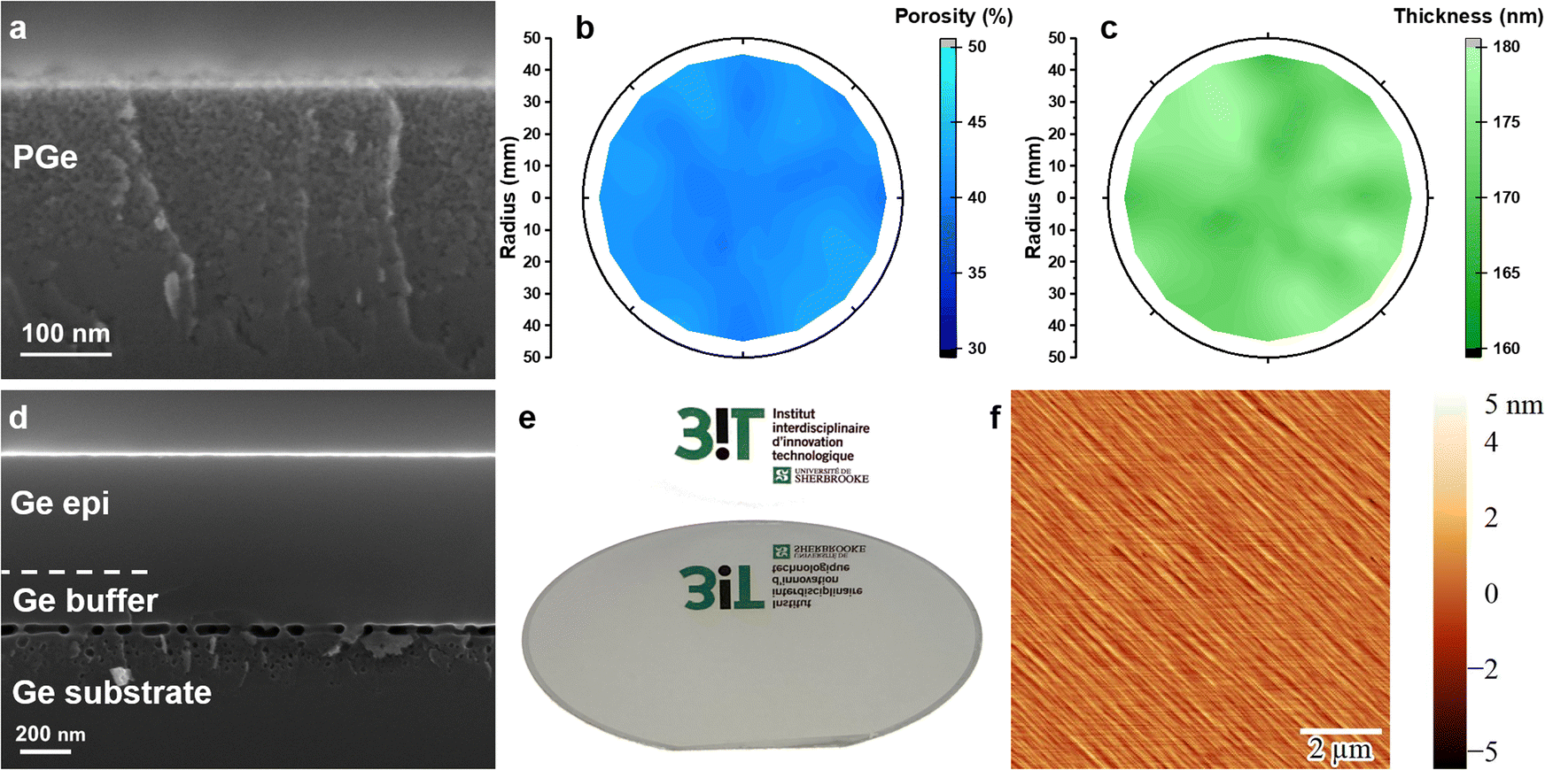 | ||
| Fig. 2 (a) Cross-sectional SEM image of the PGe layer. Ellipsometry mapping of the (b) porosity and (c) thickness across the 100 mm PGe wafer. (d) Cross-sectional SEM image of the epitaxial Ge NM. (e) Optical image of a typical epitaxial Ge grown on PGe/Ge at the wafer-scale. (f) AFM scan of the Ge NM surface with a RMS roughness of 0.7 nm. | ||
Ge epitaxial growth on the PGe substrate results in a 700 nm-thick Ge NM structure, composed of the 200 nm-thick LT Ge buffer layer and the 500 nm-thick HT epitaxial Ge, as shown by the cross-sectional SEM image of the structure in Fig. 2d. The initial LT Ge buffer has a purpose to create a crystalline seeding layer for further growth,25 as well as to cap the porous structure and confine it to the PGe/Ge buffer interface. Once a fully densified Ge buffer layer is obtained on top of the PGe structure, the final thickness of the Ge NM can be tuned by growth time and growth rate during the HT growth.
As revealed by the SEM cross-sectional image (Fig. 2d), the PGe morphology is significantly reorganized during the HT annealing and the HT growth. This porous transformation is based on the Ostwald ripening and Rayleigh instability,24,32 which allows the formation of the weak layer, and facilitates the separation of the Ge epilayer from the substrate. The pillars in the weak layer provide the mechanical stability of the NM and enable its subsequent lift-off. Similar shape transformations into a voided region have been reported for porous structures of other semiconductor materials such as Si,33,34 InP (ref. 35) and GaN.36,37
After the growth, the visual inspection of the 100 mm Ge NM shows a mirror-like surface (Fig. 2e). To further investigate the surface quality of the Ge NM, an AFM surface analysis was performed. Fig. 2f shows a smooth surface with an RMS roughness of 0.7 nm, which is close to the roughness of the parent Ge epi-ready substrate (RMS roughness ∼0.3 nm).
To determine the crystal quality, the Ge NM was characterized by HRTEM along the zone axis [110]. The cross-sectional image of the Ge NM structure (Fig. 3a) shows three regions: the Ge substrate, the weak layer, and the Ge NM. No defects nor dislocations are observed in the Ge epi-layer, which is further supported by HRTEM zoom at the pillar/Ge buffer interface shown in Fig. 3b. This also demonstrates that the crystalline continuity between the pillars and Ge NM is conserved and rules out the presence of dislocations inside of the buffer layer. This is expected, as there is no strain introduced during the homoepitaxial growth of Ge on PGe. The selected area electron diffraction (SAED) pattern obtained from Ge NM (Fig. 3a-1) shows diffraction spots corresponding to a monocrystalline pattern of Ge. Moreover, the Ge epilayer pattern is identical to the one from the substrate (Fig. 3a-2). This confirms that the crystallographic information was transmitted from the substrate to the Ge NM. This preservation of the crystalline quality is also supported by the similarity of the crystallographic planes' orientation, shown by the high-resolution zoomed images of the Ge NM and the substrate (Fig. 3c-e). Fourier mask filtering tools and the inverse fast Fourier transform (IFFT) were applied to determine the interplanar spacing, shown by generated lattice fringes for the Ge NM and bulk Ge in Fig. 3d–f, respectively. In these figures, the lattice fringes of the (1−11) planes are indicated by two parallel lines. The interplanar spacing is approximately 0.33 nm for both Ge NM and Ge, which is in agreement with the d1−11 of the diamond cubic structure of Ge.38 Therefore, HRTEM observations demonstrate the successful growth of single-crystal Ge on PGe/Ge substrates with the same crystal orientation.
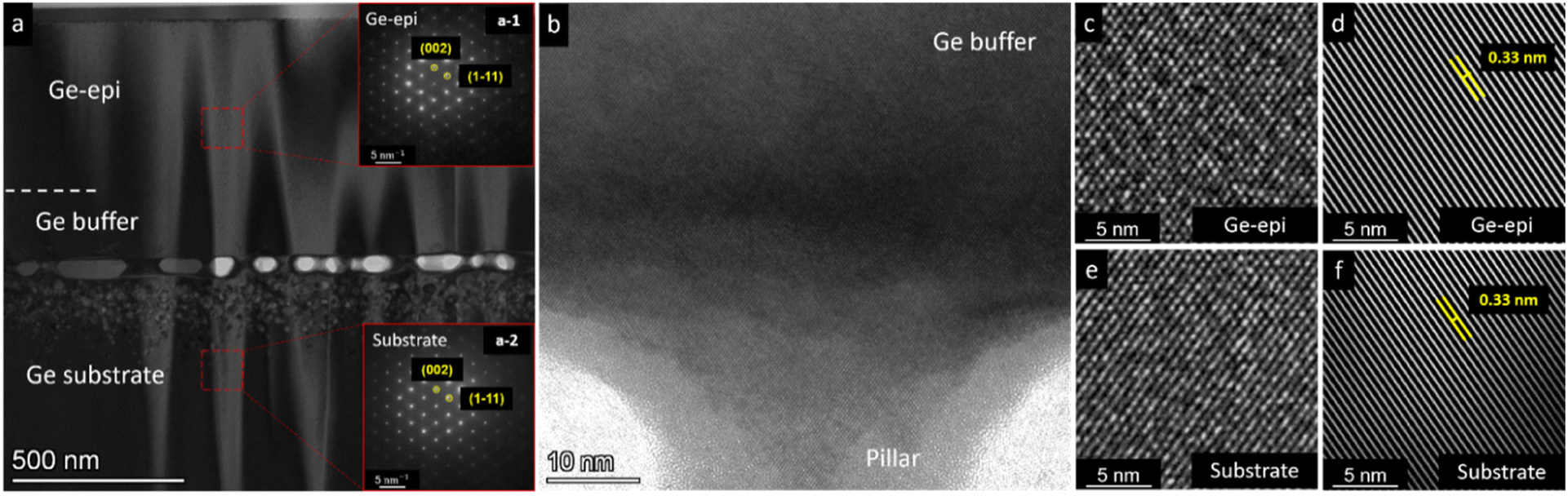 | ||
| Fig. 3 (a) Cross sectional TEM image of the epi-layer Ge structure, the contrast variation is due to thickness fringes induced by focused ion beam (FIB) milling. Insets in (a) are the selected-area electron diffraction (SAED) patterns from the Ge epi-layer (a-1) and substrate (a-2), taken along the [110] zone axis. (b) HRTEM of the Ge-epi/PGe interface. (c) HRTEM of the Ge epi-layer. (d) The inverse fast Fourier transform (IFFT) from the Ge epi-layer showing only (1−11) crystalline planes. (e) HRTEM from the Ge substrate. (f) IFFT from bulk Ge displaying only the (1−11) crystalline plane. | ||
3.2. GaAs growth on the Ge/PGe structure
To demonstrate the viability of detachable Ge NMs for the growth of III–V compounds, a 400 nm GaAs layer was grown on top of the Ge NM. The structural quality of the GaAs/Ge/PGe structure was evaluated by HRXRD in the ω–2θ configuration, around (004) symmetric and (115) asymmetric atomic planes (Fig. 4a and b). For the (004) plane, the full width at half maximum (FWHM) of the Ge NM diffraction peak is 15 ± 4 arcs, which is comparable to the value of bulk Ge (14 ± 4 arcs). The FWHM of the GaAs on the Ge/PGe diffraction peak is 80 ± 4 arcs, matching with the GaAs reference grown on bulk Ge (76 ± 4 arcs) (as shown in Fig. S3 of the ESI†). The Ge and GaAs peaks are sharp and show no significant broadening, which proves the same quality as the GaAs reference.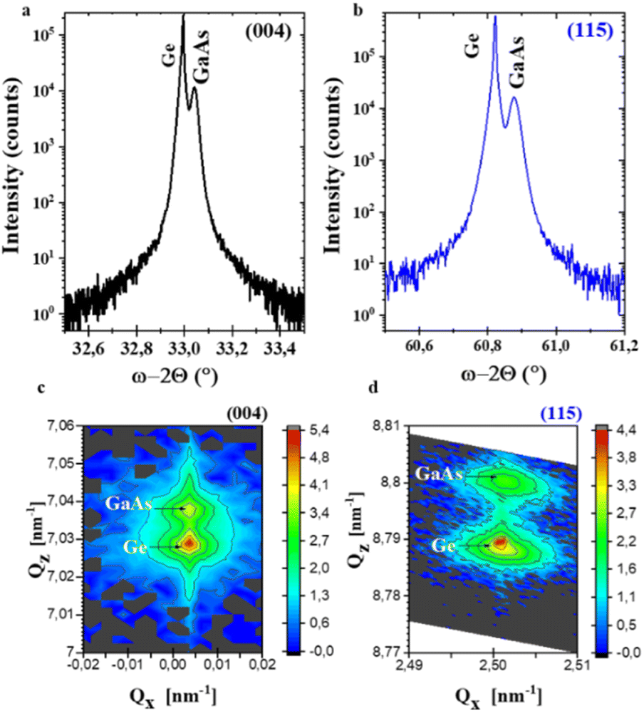 | ||
| Fig. 4 HRXRD analysis of GaAs on Ge taken around (004) (a) and (115) (b) reflections. (c) Triple axis reciprocal space (RSM) around (004) and (d) asymmetric (115). | ||
Fig. 4c and d display measured reciprocal space mapping (RSM) of the structure around (004) and (115) planes, respectively. Each RSM shows two distinct reciprocal lattice-point maxima corresponding to Ge and GaAs epitaxial layers, plotted as a function of their respective reciprocal space axes Qx (in-plane) and Qz (out-of-plane). GaAs and Ge peaks are well aligned along the vertical direction, which means that the GaAs was grown pseudo-morphically. This behavior can be explained by the fact that the deposited GaAs thickness is below the critical thickness,39 leaving a fully strained layer. These results demonstrate the compatibility of Ge NMs with III–V materials.
3.3. Substrate reconditioning and reuse
To assess the possibility of reusing the parent Ge wafers at the end of the process, we have designed a cost-effective reconditioning method of the Ge substrate through a wet etching of the surface.27 After Ge NM separation, the RMS surface roughness of the substrate is 20.1 nm (Fig. 5a–c). This is due to the presence of porous layer residues (Fig. S4 of the ESI†). This leads to the formation of an inhomogeneous PGe layer with defects, making it unsuitable for a further epitaxial regrowth.40,41 To remove these residues, the substrate was etched in a HF-based aqueous solution, with H2O2.27 The combined use of an oxidizing agent (H2O2) and an etching agent (HF) allows etching of the substrate surface.42 Then, we demonstrated that a high concentration of H2O2 compared to HF and water resulted in an efficient surface flattening with an RMS roughness of 1.3 nm (Fig. 5-d).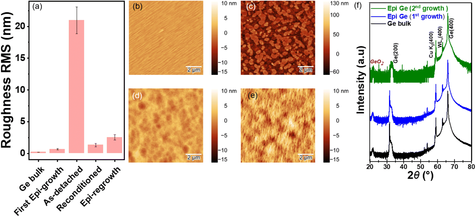 | ||
| Fig. 5 (a) RMS roughness evolution at different steps of the reconditioning process (b–e) AFM scan results (10 × 10 μm in tapping mode) of (b) after the first epi-growth, (c) as-detached substrate, (d) reconditioned substrate and (e) after epi-regrowth. (f) 2θ scan of the Ge substrate, first epitaxial Ge grown on a PGe/Ge template and epitaxial Ge regrown on PGe/Ge after the reconditioning. | ||
This makes the reconditioned substrate suitable for the reporosification and results in a PGe layer with a roughness around 2.2 nm, which is comparable to that of the PGe layer on the epi-ready substrate (∼2 nm Fig. S2†). This value is low-enough to ensure the suitability of the reporosified substrate for a new epitaxial growth. Finally, after a second epitaxial growth of Ge, the roughness of the epitaxial layer was measured at 2.5 nm (Fig. 5a–e). This value remains low enough for a new epitaxial growth of GaAs as achieved after the first growth of Ge (RMS = 0.7 nm in Fig. 5a and b). Fig. 5f shows the standard wide-angle XRD of the Ge epilayer grown on the stack PGe/reconditioned substrate. XRD patterns of the bulk Ge substrate and the Ge epilayer (1st) growth are also included as a reference. The (002) and (004) reflections agree with those of the reference. The structural investigations rule out the presence of amorphous or polycrystalline domains and suggest the formation of a monocrystalline structure. These results demonstrate a reuse sequence without loss of the surface or crystalline quality of the Ge epilayer and emphasize the effectiveness of the PEELER approach.
3.4. Ge consumption analysis
The PEELER approach significantly reduces the portion of Ge used for device fabrication compared to conventional Ge wafers.43 As shown in Fig. 6, in the case of a conventional 100 mm Ge wafer substrate (not reused), having 145 μm of thickness, 6.06 g of Ge is passed onto the device processing, e.g., solar cell production. During this manufacturing process, about 2.72 g of Ge is lost because of wafer thinning down to 80 μm.44 On the other hand, following the PEELER approach, a substrate is expected to be reused multiple times for device manufacturing (Fig. 6). Taking into consideration the growth of a 5 μm Ge layer, as it is a thickness sufficient for a Ge bottom cell,45 only 0.21 g of Ge is consumed for solar cell fabrication. Adding up 0.06 g of Ge lost during wastewater recycling, only 0.27 g of Ge is used per cycle. This represents more than 95% reduction of Ge consumption compared to conventional Ge wafers. Moreover, by using 600 μm Ge wafers, the substrate can be reused for up to 30 times before it becomes too fragile for manipulation and is recycled. Use of thick wafers in the process limits also the loss of Ge due to the wafer sawing and wastewater treatments during the initial wafer production.46,47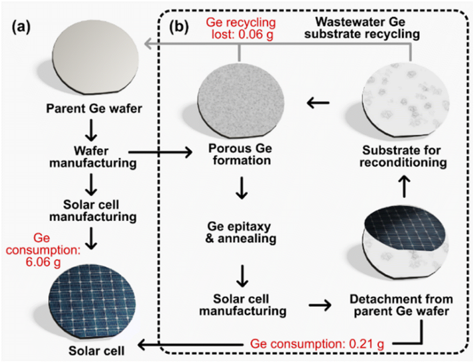 | ||
| Fig. 6 Comparison of Ge consumption between (a) the conventional Ge wafer pathway and (b) the PEELER approach illustrated in the case of solar cell fabrication. | ||
4. Conclusions
With the PEELER approach, we demonstrated the fabrication of detachable monocrystalline Ge NMs and substrate reuse. The proposed approach uses a BEE process, which is demonstrated on 100 mm Ge wafers and allows the production of uniform PGe layers. The PGe/Ge substrate is then used to grow high-quality monocrystalline Ge NMs. The morphological transformation of PGe during the HT annealing enables the detachment of the Ge NMs. Thus, the produced Ge NMs are suitable for the epitaxial growth of III–V materials.After detachment of the Ge NM, the reconditioning of the Ge substrate was achieved using a HF-based chemical solution to selectively remove porous layer residues. This treatment reduces the RMS roughness of the substrate from 20 nm to 1.3 nm allowing the process to be repeated on the used substrate. Monocrystalline Ge NMs were again obtained with a surface quality suitable for III–V growth for solar cells. The PEELER process enables the production of multiple Ge NMs from a single substrate at the wafer-scale. A case study of its impact on the sustainability of space solar cell production was presented, where we estimated 0.27 g of Ge consumption per PEELER cycle compared to 6.06 g consumed by the conventional wafer strategy.
Finally, this approach implements a sustainable process flow by achieving a significant reduction of Ge consumption in a real case device fabrication. It implies a positive effect by avoiding unnecessary resource depletion produced by the current Ge wafer processing. Moreover, the Ge NMs take advantage of low mass and flexibility and offer a platform for a new generation of Ge and III–V based lightweight and flexible high-performance optoelectronic devices.
Author contributions
N. Paupy, Z. O. Elhmaidi, A. Chapotot, T. Hanuš and J. Arias-Zapata contributed equally to this work. N. Paupy, Z. O. Elhmaidi, A. Chapotot, T. Hanuš, J. Arias-Zapata: conceptualization, methodology, validation, formal analysis, investigation, writing – original draft, writing – review & editing, visualization, supervision. B. Ilahi: conceptualization, methodology, validation, writing – review & editing, supervision. A. Heintz, A. B. P. Mbeunmi: conceptualization, methodology, investigation, writing – review & editing. R. Arvinte, M. R. Aziziyan: validation, supervision, writing – review & editing V. Daniel, F. Zouaghi, A. Ayari, L. Mouchel, J. Henriques, L. Demoulin, H. Pelletier: data analysis, writing – review & editing. G. Hamon: writing – review & editing, supervision. J. Chrétien: writing – review & editing, supervision, T. Mamoudou Diallo: investigation, writing – review & editing, supervision M. Volatier: supervision, writing – review & editing. R. Kurstjens, J. Cho, G. Courtois, K. Dessein, S. Arcand, C. Dubuc: data analysis, validation, writing – review & editing. A. Jaouad, N. Quaegebeur, R. Gosselin, D. Machon, R. Arès: data analysis, validation, writing – review & editing, supervision. M. Darnon: data analysis, validation, writing – review & editing, supervision. A. Boucherif: conceptualisation, methodology, data analysis, validation, writing – review & editing, supervision, project planning, funding acquisition.Conflicts of interest
There are no conflicts to declare.Acknowledgements
The authors thank Guillaume Bertrand, René Labrecque and the 3IT's clean room staff for technical support. The authors also thank Carmen Andrei and Brian Langelier from Mc Master University for TEM observations, the Natural Sciences and Engineering Research Council of Canada (NSERC), Innovation en énergie électrique (InnovÉÉ), Mitacs, and Umicore and Saint-Augustin Canada Electric (Stace) for financial support. Abderraouf Boucherif is grateful for a Discovery grant supporting this work. A special mention is addressed to others, who have contributed to achieve the above results: Stéphanie Sauze, Arthur Dupuy, Sofiane Abdelouhab, Mohamed El-Gahouchi, Sara Taslimi, Samuel Cailleaux, Graniel Harne Abrenica, Brieuc Mével, Jérôme Deshaies, Mazarine Polydore, Quentin Reboul, Santiago Pereira, Zachary Thuotte, Antony Marcoux, Adam Dufour, Rose-Marie Pelletier, Sara Houde, Joel Dufault, Pascal Berube, Jérémy Beauchamp, and Lucas Jempson. LN2 is a joint International Research Laboratory (IRL 3463) funded and co-operated in Canada by Université de Sherbrooke and in France by CNRS as well as ECL, INSA Lyon, and Université Grenoble Alpes (UGA). It is also supported by the Fonds de Recherche du Québec Nature et Technologie (FRQNT).Notes and references
- J. A. Rogers, M. G. Lagally and R. G. Nuzzo, Nature, 2011, 477, 45–53 CrossRef CAS PubMed.
- H. Kum, D. Lee, W. Kong, H. Kim, Y. Park, Y. Kim, Y. Baek, S.-H. Bae, K. Lee and J. Kim, Nat. Electron., 2019,(2), 439–450 CrossRef CAS.
- M. Sistani, R. Böckle, D. Falkensteiner, M. A. Luong, M. I. den Hertog, A. Lugstein and W. M. Weber, ACS Nano, 2021, 15, 18135–18141 CrossRef CAS PubMed.
- R. Kaufmann, G. Isella, A. Sanchez-Amores, S. Neukom, A. Neels, L. Neumann, A. Brenzikofer, A. Dommann, C. Urban and H. von Känel, J. Appl. Phys., 2011, 110, 023107 CrossRef.
- D. Fan, K. Lee and S. R. Forrest, ACS Photonics, 2016, 3, 670–676 CrossRef CAS.
- S. Lischke, A. Peczek, J. S. Morgan, K. Sun, D. Steckler, Y. Yamamoto, F. Korndörfer, C. Mai, S. Marschmeyer, M. Fraschke, A. Krüger, A. Beling and L. Zimmermann, Nat. Photonics, 2021, 15, 925–931 CrossRef CAS.
- S. Park, J. Simon, K. L. Schulte, A. J. Ptak, J. S. Wi, D. L. Young and J. Oh, Joule, 2019, 3, 1782–1793 CrossRef CAS.
- J. Friedrich, in Reference Module in Materials Science and Materials Engineering, Elsevier, 2016 Search PubMed.
- W. von Ammon, Phys. Status Solidi A, 2014, 211, 2461–2470 CrossRef CAS.
- G. Van Hoof, M. Schurmans, B. Robertz, J.-F. Ménard and K. Dessein, J. Sustain. Metall., 2020, 6, 333–343 CrossRef.
- D. Shahrjerdi, S. W. Bedell, C. Ebert, C. Bayram, B. Hekmatshoar, K. Fogel, P. Lauro, M. Gaynes, T. Gokmen, J. A. Ott and D. K. Sadana, Appl. Phys. Lett., 2012, 100, 053901 CrossRef.
- T. Ataser, M. K. Ozturk, O. Zeybek and S. Ozcelik, Acta Phys. Pol., A, 2019, 136, 21–25 CrossRef CAS.
- I. Lombardero, L. Cifuentes, M. Gabás and C. Algora, Prog. Photovolt. Res. Appl., 2022, 3547 Search PubMed.
- G. Van Hoof, M. Schurmans, B. Robertz, J. F. Ménard and K. Dessein, J. Sustain. Metall., 2020, 6, 333–343 CrossRef.
- K. A. Horowitz, T. W. Remo, B. Smith and A. J. Ptak, A Techno-Economic Analysis and Cost Reduction Roadmap for III–V Solar Cells, National Renewable Energy Lab. (NREL), Golden, CO (United States), 2018 Search PubMed.
- I. Radu, A. Boussagol, A. Barthelemy and S. Vincent, ECS Trans., 2008, 16, 349–360 CrossRef CAS.
- M. Kim, S. J. Cho, Y. J. Dave, H. Mi, S. Mikael, J.-H. Seo, J. U. Yoon and Z. Ma, Semicond. Sci. Technol., 2018, 33, 015017 CrossRef.
- C.-W. Cheng, K.-T. Shiu, N. Li, S.-J. Han, L. Shi and D. K. Sadana, Nat. Commun., 2013, 4, 1577 CrossRef PubMed.
- W. H. Chang, H.-W. Wan, Y.-T. Cheng, Y.-H. G. Lin, T. Irisawa, H. Ishii, J. Kwo, M. Hong and T. Maeda, Jpn. J. Appl. Phys., 2022, 61, SC1024 CrossRef.
- J. Chen and C. E. Packard, Sol. Energy Mater. Sol. Cells, 2021, 225, 111018 CrossRef CAS.
- J. S. Mangum, A. D. Rice, J. Chen, J. Chenenko, E. W. K. Wong, A. K. Braun, S. Johnston, H. Guthrey, J. F. Geisz, A. J. Ptak and C. E. Packard, Adv. Energy Mater., 2022, 12, 2201332 CrossRef CAS.
- V. Depauw, C. Porret, M. Moelants, E. Vecchio, K. Kennes, H. Han, R. Loo, J. Cho, G. Courtois, R. Kurstjens, K. Dessein, V. Orejuela, C. Sanchez-Perez, I. Rey-Stolle and I. García, Prog. Photovolt. Res. Appl., 2022, 3634 CrossRef.
- E. Winter, W. Schreiber, P. Schygulla, P. L. Souza, S. Janz, D. Lackner and J. Ohlmann, J. Cryst. Growth, 2023, 602, 126980 CrossRef CAS.
- A. Boucherif, G. Beaudin, V. Aimez and R. Arès, Appl. Phys. Lett., 2013, 102, 011915 CrossRef.
- T. Hanuš, B. Ilahi, A. Chapotot, H. Pelletier, J. Cho, K. Dessein and A. Boucherif, Mater. Today Adv., 2023, 18, 100373 CrossRef.
- T. Hanuš, J. Arias-Zapata, B. Ilahi, P. Provost, J. Cho, K. Dessein and A. Boucherif, Adv. Mater. Interfaces, 2023, 10, 2202495 CrossRef.
- A. Chapotot, B. Ilahi, J. Arias-Zapata, T. Hanuš, A. Ayari, G. Hamon, J. Cho, K. Dessein, M. Darnon and A. Boucherif, Germanium Surface Wet-Etch-Reconditioning for Porous Lift-off and Substrate Reuse, (to be published) Search PubMed.
- G. H. A. Abrenica, M. V. Lebedev, G. Okorn, D. H. van Dorp and M. Fingerle, Appl. Phys. Lett., 2018, 113, 062104 CrossRef.
- P. Ponath, A. B. Posadas and A. A. Demkov, Appl. Phys. Rev., 2017, 4, 021308 Search PubMed.
- A. B. Poungoué Mbeunmi, R. Arvinte, H. Pelletier, M. Jellite, R. Arès, S. Fafard and A. Boucherif, J. Cryst. Growth, 2020, 547, 125807 CrossRef.
- T. M. Diallo, A. B. Poungoué Mbeunmi, M. El-Gahouchi, M. Jellite, R. Arvinte, M. R. Aziziyan, R. Arès, S. Fafard and A. Boucherif, J. Vac. Sci. Technol., B: Nanotechnol. Microelectron.: Mater., Process., Meas., Phenom., 2019, 37, 031208 Search PubMed.
- S. Tutashkonko, T. Nychyporuk, V. Lysenko and M. Lemiti, J. Appl. Phys., 2013, 113, 023517 CrossRef.
- N. Milenkovic, M. Drießen, C. Weiss and S. Janz, J. Cryst. Growth, 2015, 432, 139–145 CrossRef CAS.
- S. Kajari-Schröder, J. Käsewieter, J. Hensen and R. Brendel, Energy Procedia, 2013, 38, 919–925 CrossRef.
- X. Kou and M. S. Goorsky, ECS Trans., 2013, 50, 325–330 CrossRef.
- J. H. Kang, J. Key Lee and S. W. Ryu, J. Cryst. Growth, 2012, 361, 103–107 CrossRef CAS.
- S. Huang, Y. Zhang, B. Leung, G. Yuan, G. Wang, H. Jiang, Y. Fan, Q. Sun, J. Wang, K. Xu and J. Han, ACS Appl. Mater. Interfaces, 2013, 5, 11074–11079 CrossRef CAS PubMed.
- T. M. Diallo, M. R. Aziziyan, R. Arvinte, J. Harmand, G. Patriarche, C. Renard, S. Fafard, R. Arès and A. Boucherif, Small, 2021, 2101890 Search PubMed.
- G. Timoò, C. Flores, B. Bollani, D. Passoni, C. Bocchi, P. Franzosi, L. Lazzarini and G. Salviati, J. Cryst. Growth, 1992, 125, 440–448 CrossRef.
- I. Rey-Stolle, E. Barrigón, B. Galiana and C. Algora, J. Cryst. Growth, 2008, 310, 4803–4807 CrossRef CAS.
- L. Magagnin, J. Poortmans, Y. Abdulraheem, J. Szlufcik, I. Gordon, M. Debucquoy, T. Bearda, H. Sivaramakrishnan Radhakrishnan, V. Depauw, I. Sharlandzhiev, K. Van Nieuwenhuysen and A. Hajijafarassar, 32nd Eur. Photovolt. Sol. Energy Conf. Exhib., 2016, pp. 313–316 Search PubMed.
- S. Sioncke, Y. J. Chabal, M. M. Frank, J. Bardeen, W. Brattain and W. Shockley, Handb. Clean. Semicond. Manuf. Fundam. Appl., 2011, 429–472 CAS.
- J. Fernandez, S. Janz, D. Suwito, E. Oliva and F. Dimroth, in 2008 33rd IEEE Photovoltaic Specialists Conference, 2008, pp. 1–4 Search PubMed.
- SPACE Solar Cells – AZUR SPACE Solar Power GmbH, http://www.azurspace.com/index.php/en/products/products-space/space-solar-cells, accessed March 7, 2022 Search PubMed.
- I. Lombardero, M. Ochoa, N. Miyashita, Y. Okada and C. Algora, Prog. Photovolt. Res. Appl., 2020, 28, 1097–1106 CrossRef CAS.
- R. L. Meek and M. C. Huffstutler, J. Electrochem. Soc., 1969, 116, 893 CrossRef CAS.
- F. Arroyo Torralvo, C. Fernández-Pereira, E. García Villard, Y. Luna, C. Leiva, L. Vilches and R. Villegas, Miner. Eng., 2018, 128, 106–114 CrossRef CAS.
Footnotes |
| † Electronic supplementary information (ESI) available. See DOI: https://doi.org/10.1039/d3na00053b |
| ‡ These authors equally contributed to the manuscript. |
| This journal is © The Royal Society of Chemistry 2023 |