
 Open Access Article
 This Open Access Article is licensed under a
 Creative Commons Attribution 3.0 Unported Licence
Improved photovoltaic performance of Pb-free AgBi2I7 based photovoltaics†
Praveen
Kumar
a,
Khursheed
Ahmad
a and
Shaikh M.
Mobin
 *abc
*abc
aDepartment of Chemistry, Indian Institute of Technology Indore, Simrol, Khandwa Road, Indore 453552, India. E-mail: xray@iiti.ac.in
bDepartment of Biosciences and Bio-Medical Engineering, Indian Institute of Technology Indore, Simrol, Khandwa Road, Indore 453552, India
cCenter for Advanced Electronics (CAE), Indian Institute of Technology Indore, Simrol, Khandwa Road, Indore 453552, India
First published on 16th February 2023
Abstract
Hybrid perovskites based on bismuth are good candidates for developing lead-free and air-stable photovoltaics, but they have historically been constrained by poor surface morphologies and large band-gap energies. Monovalent silver cations are incorporated into iodobismuthates as part of a novel materials processing method to fabricate improved bismuth-based thin-film photovoltaic absorbers. However, a number of fundamental characteristics prevented them from achieving better efficiency. We examine bismuth iodide perovskite made of silver with improvements in surface morphology and a narrow band gap, and we achieve high power conversion efficiency. AgBi2I7 perovskite was used in the fabrication of PSCs as a material for light absorption, and its optoelectronic proficiencies were also studied. We reduced the band gap to 1.89 eV and achieved a maximum power conversion efficiency of 0.96% using the solvent engineering approach. Additionally, simulation studies verified an efficiency of 13.26% by using AgBi2I7 as a light absorber perovskite material.
Due to their exceptional semiconducting characteristics, such as relatively low carrier recombination rates,1,2 long carrier diffusion lengths,2 low charge carrier mobilities,3,4 stoichiometry-tunable band gaps,5,6 and high absorption coefficients, lead-based halide perovskites have recently attracted a lot of attention.7 Formamidinium lead iodide (FAPbI3), one of the perovskite systems, has drawn the most interest because of its outstanding performance in thin-film solar cells, where it can achieve a power conversion efficiency (PCE) of 25.7%.8 However, the presence of noxious Pb and the product's fragility when exposed to moisture and temperature have led to grave worries about its viability for commercial use. There has been a lot of interest in developing halide perovskite solar cells that are non or low-toxic and air stable. As a result, efforts have been made to develop perovskite solar cells and seek alternatives to lead. Many perovskites based on tin (Sn)9 and germanium (Ge)10 have been investigated to address the issue of toxicity. Song et al.11 designed and manufactured Sn-based perovskite materials containing caesium (Cs) as a cation, with CsSnI3 and CsSnBr3 perovskites achieving efficiencies of 3.04% and 1.83%, respectively. In addition, Ke et al.12 used a unique hollow 3-D perovskite [enFASnI3] as a light absorber material in perovskite solar cells (PSCs), with a 7.1% efficiency. Mhaisalkar and colleagues used a Ge-based AGeI3 perovskite-like material.13 These Sn and Ge based perovskite-like materials have a high efficiency, but they must be handled with caution since they are air sensitive and need an inert environment to be stable. The perovskite structure is distorted by the quick shift in the oxidation states of Sn and Ge by +2. Moreover, when compared to Pb, these Sn and Ge based perovskites are unable to reach high efficiency. However, instability and poor performance of Sn and Ge based devices under ambient conditions owing to disproportionation are disappointing.
There have been several reports on the use of copper (Cu) as a metal ion in PSCs, utilising a lead-free approach. Mathews et al.,14 Ahmad et al.,15 and Li et al.16 utilized MA2CuClxBr4−x and C6H4NH2CuBr2I perovskite materials as light absorbers in photovoltaic applications. Although these Cu-based perovskites have high stability, they are inefficient in producing good PCE. Yang et al.,17 Wang et al.,18 and Vargas et al.19 studied the optoelectronic activity of (C6H5CH2NH3)2CuBr4, (H3NC6H4NH3)CuBr4, and Cs4CuSb2Cl12 perovskite materials, respectively. Further, lead(II), bismuth (Bi3+), and antimony (Sb3+) ions are isoelectronic (6s2), and they may be stable and safe substitutes in thin-film photovoltaic (PV) systems. Bi3+ may be used to manufacture PSCs as a non-toxic metal ion, which is promising for replacing Pb and Sn metals. The A3Bi2I9 basic formula (A = Cs+, MA+, NH4+, B = Bi3+, Sb3+, X = Cl−, Br−, I−) has been widely employed in the design and manufacture of lead-free perovskite solar cells. Mobin et al.20 created Cs3Sb2I9 and Cs3Bi2I9 perovskites with a PCE of above 1%. Hebig et al.21 and Ahmad et al.22 used MA3Sb2I9 for photovoltaic applications, whereas Kumar et al.23 and Zuo et al.24 used (NH4)3Sb2I9 perovskite as the light absorber and developed a device that demonstrated the potential of Bi3+ in PSCs. Okano et al.25 and Ahmad et al.26 employed a gas-assisted and two-step manufacturing technique to prepare (CH3NH3)3Bi2I9 for PSCs, respectively. Kulkarni et al.27 used an N-methyl pyrrolidone-assisted method and achieved 0.31% PCE. Huang et al.28 obtained 0.06% PCE using fluorinated perylene diimide (FPDI) as an ETL (electron transport layer) in the (CH3NH3)3Bi2I9 PSC. This low PCE might be due to the FPDI's weak surface or charge extraction issue. Sun et al.29 and Zhuang et al.,30 on the other hand, looked into the crystalline properties of (NH4)3Bi2I9 perovskite and used it in X-rays and PSCs, respectively. Furthermore, their broad band gap and low PCE reduce the likelihood of commercialization. To improve photovoltaic efficiency, 3D structures based on silver-bismuth iodide are used. Filip et al. suggested double halide perovskites like Cs2BiAgCl6 and Cs2BiAgBr6 in 2016.31 AgBi2I7 perovskite has recently attracted interest because of its efficiency and narrow band gap (<2.0 eV), which improve light harvesting characteristics. Kim et al.32 reported the first Ag-based PSC using Bi as the metal ion in 2016 and attained a PCE of 1.2%. However, when Shao et al.33,34 and Johansson et al.35 employed the same methodology, the performance of AgBi2I7 perovskite changed with photovoltaic efficiency. Reproducing the solar cell yielded just 0.52 and 0.4% efficiency.33–35 AgBi2I7 perovskite's sensitivity can make up for its lack of repeatability, or it could be caused by the annealing temperature. To comprehend and modify the attributes of Ag-based Bi PSCs, we synthesised AgBi2I7 (SBI).
We have studied the solution engineering approach to improve the photovoltaic performance of silver-based bismuth iodide perovskites as light absorbers. To our knowledge, this is the first report on the use of SBI perovskites as light absorbers in the presence of DMF and DMF![[thin space (1/6-em)]](https://www.rsc.org/images/entities/char_2009.gif) :MeOH. The impact of the solvent engineering strategy on the fabrication of SBI perovskite solar cells may be immediately seen in their efficiency and photovoltaic properties. In the present work, we employed DMF and MeOH, two different solvents in an appropriate ratio, and with molar ratio 1:2 of AgI and BiI3 respectively. AgBi2I7 DMF (SBI-D) and AgBi2I7 DMF:MeOH (SBI-DM) were spin coated onto the conductive glass electrode (FTO) at 1500 rpm for 30 seconds (Scheme 1). Other fabrication data are provided in the ESI.† A convincing demonstration of the equimolar ratio of both the solvent (DMF:MeOH) gives the highest PCE as compared to only 0.96% with DMF under 1 sun illumination conditions and 30–40% humidity.
:MeOH. The impact of the solvent engineering strategy on the fabrication of SBI perovskite solar cells may be immediately seen in their efficiency and photovoltaic properties. In the present work, we employed DMF and MeOH, two different solvents in an appropriate ratio, and with molar ratio 1:2 of AgI and BiI3 respectively. AgBi2I7 DMF (SBI-D) and AgBi2I7 DMF:MeOH (SBI-DM) were spin coated onto the conductive glass electrode (FTO) at 1500 rpm for 30 seconds (Scheme 1). Other fabrication data are provided in the ESI.† A convincing demonstration of the equimolar ratio of both the solvent (DMF:MeOH) gives the highest PCE as compared to only 0.96% with DMF under 1 sun illumination conditions and 30–40% humidity.
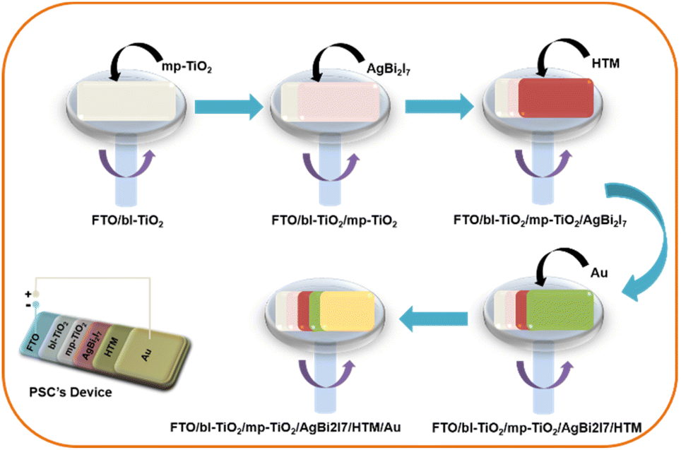 | ||
| Scheme 1 Schematic of the fabrication procedure of the perovskite solar cell. | ||
PXRD was used to characterise the phase purity and formation of the SBI perovskite material synthesized with both DMF and DMF:MeOH solvents, with the findings shown in Fig. 1A. The formation and crystalline nature of SBI-D (DMF:MeOH = 1:0) and SBI-DM (DMF:MeOH = 0.5:0.5) perovskite materials were revealed by PXRD peak patterns. The growth of SBI-D and SBI-DM is supported by the appearance of a prominent diffraction peak in the (333) plane.
 | ||
| Fig. 1 PXRD peak pattern (A) and UV-vis absorption spectra (B) of AgBi2I7 perovskite with MeOH (red) and without MeOH (black). | ||
The stability of perovskite may be assessed using the Goldschmidt tolerance factor (t); when the value of “t” is between 0.8 and 1, it implies that the perovskite structure is stable.36 Another important component in the cubic crystal is the ionic radius of A, which should not be either large (then, t > 1) or too small (then, t < 0.8) in comparison to the ionic radius of B. If the ionic radius of A is substantially bigger than that of B, it will not fit inside the BX8 octahedron. This could originate from a distinct perovskite structure. The tolerance factor and octahedron ratio are described by eqn (a) and (b):
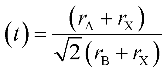 | (a) |
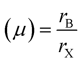 | (b) |
At t = 1, the predicted perfect cubic structure was seen. In order to produce a stable octahedron for a cubic cell, the octahedron factor (μ) should be between 0.44 and 0.72. The effective ionic radii of silver (Ag) and bismuth (Bi) are 1.26 Å and 1.03 Å, respectively, which are appropriate for the creation of a stable cubic perovskite structure. We may infer and remark on the stability of our perovskite based on this finding, and therefore, it can also be employed as a light absorber material in photovoltaic applications.
UV/vis spectroscopy was used to determine the optical characteristics of SBI-D and SBI-DM thin films (Fig. 1B). The absorption spectra of these perovskite materials were nearly identical. The optical band gaps for SBI-D and SBI-DM may be calculated using UV absorption spectra and linear extrapolation of Tauc plots (Fig. S1†).37 The optical band gap was calculated to be 1.89 eV using the Tauc plot ((αhν)n against hν), where α, h and ν are the absorption coefficient, Planck's constant, and excitation frequency respectively. The computed optical band gap reveals that the produced perovskite has high absorbance and has the potential to be used as a light absorber in solar cells.
Surface morphology investigation was done using FE-SEM to evaluate the impact of engagement and solvent content on the perovskite SBI material. The surface morphology of SBI-D and SBI-DM is shown in Fig. 2A–D, and it was obvious that only the DMF solvent produced a rod-like shape, whereas the DMF:MeOH combination produced a distorted rod-like morphology that was converted to a uniform surface morphology.
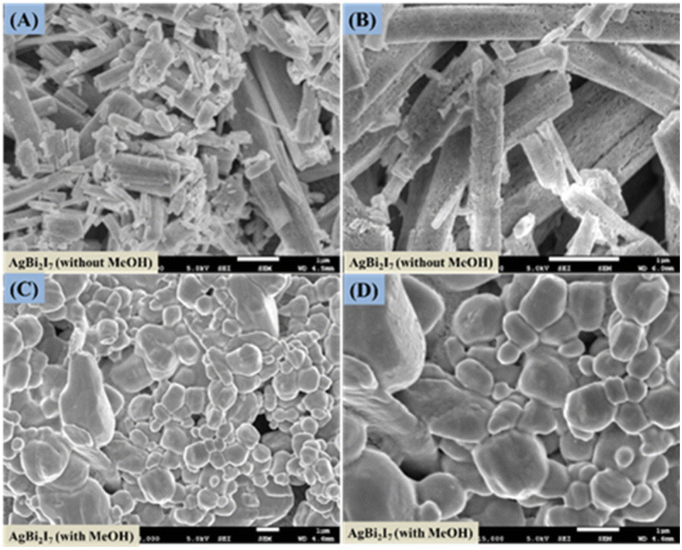 | ||
| Fig. 2 FE-scanning electron microscopy images of AgBi2I7 perovskite without MeOH (A and B) and with MeOH (C and D). | ||
This might be due to perovskite suppressing and regulating the quick crystallisation process. It has been discovered that a pinhole-free, smooth layer can improve the photovoltaic efficiency of perovskite solar cells.
When a photon strikes a perovskite material, it generates an electron and hole pair. The produced electron was excited and moved towards the LUMO (lowest unoccupied molecular orbital) level, from where it was transferred to conductive glass (FTO) through mesoporous-TiO2 and blocking-TiO2 LUMO levels. The produced electrons are contained in FTO glass, while the remaining hole in the perovskite material is carried via the HTM (hole transport material) to complete the circuit. Scheme 2 explains the entire electron transfer mechanism in simple terms. All of the energy levels of the conductive glass, ETL, and HTM, such as bl-TiO2, mp-TiO2, Spiro-MeOTAD, and Au, have been extracted from previously published literature. In addition, using UV-visible and cyclic voltammetry (CV) techniques, the HOMO–LUMO energy levels of our perovskite materials SBI were estimated similarly to previous reports.
 | ||
| Scheme 2 Schematic device structure (A) and materials energy level diagram (B) of the SBI based PSCs. Energy level values as per reported literature. | ||
The optical band gap of SBI was determined using a Tauc plot, whereas the onset reduction potential (Ered) was determined using a CV graph (Fig. S2†). We determine the energy levels of the SBI perovskite material using eqn (i) and (ii).38 All of the CV measurement details are included in the ESI.†
| ECB (ELUMO) = −(Ered + 4.725) eV | (i) |
| EVB (EHOMO) = −(ECB − Eg) eV | (ii) |
Henceforth, we compared our computed SBI perovskite energy levels (ECB and EVB) to the ETL and HTM for smooth charge transfer. The results indicate an excellent correlation between the HOMO and LUMO levels, implying that SBI perovskite has potential as a light absorber material.
Moreover, a PSC device was designed using AgBi2I7 as a perovskite light absorber; comprehensive device fabrication details are included in the ESI†. The device's photovoltaic performance was measured after it was fabricated under ambient conditions (30–40% humidity). The short circuit photocurrent density–voltage curve was used to assess the device's photovoltaic performance. Fig. 3 shows the photovoltaic performance of SBI-D and SBI-DM under one sun conditions (1.5 AM; 100 mW cm−2). Table 1 contains all of the photovoltaic parameters recorded by the devices. The maximum PCE of 0.96% was reached using SBI-DM PSCs, which is higher than the PCE of PSCs manufactured with SBI-D as a light absorber. Additionally, Fig. S5, ESI† provides the box charts of the Jsc, FF, Voc, and PCE for SBI-D and SBI-DM. Moreover, SBI-DM perovskite as a light absorber attained a higher open circuit voltage than SBI-D PSCs. However, AgBi2I7 synthesized from DMF and MeOH solutions revealed homogeneous grains and a thin uniform layer, providing an easy interaction with surrounding charge transfer layers. It is observed from the XRD and SEM results that the solvent in the precursor solution significantly affects the crystallization and morphology of AgBi2I7. This solvent engineering approach showed the improvement in morphology without affecting the perovskite structure, which resulted in an increase in efficiency.
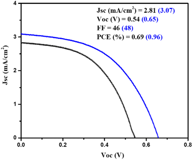 | ||
| Fig. 3 Showing the photovoltaic performance of SBI-D and SBI-DM under 1 sun conditions. | ||
| Light absorbers | V oc (mV) | FF (%) | J sc (mA cm−2) | PCE (%) | References |
|---|---|---|---|---|---|
| (CH3NH3)3Sb2I9 | 896 | 55 | 1.0 | 0.49 | 21 |
| C6H4NH2CuBr2I | 200 | 46 | 6.2 | 0.46 | 16 |
| Cs2SnI6 | 520 | 52 | 3.2 | 0.86 | 39 |
| AgBi2I7 | 690 | 43 | 2.76 | 0.83 | 40 |
| (CH3NH3)3Sb2I9 | 740 | 52 | 1.48 | 0.57 | 41 |
| Cs2NaBiI6 | 470 | 44 | 1.99 | 0.42 | 42 |
| Cs3Bi2I9 | 570 | 222 | 49 | 0.62 | 43 |
| (NH4)3Sb2I9 | 1003 | 115 | 42.9 | 0.51 | 44 |
| CH3NH3SnBr3 | 490 | 46 | 2.2 | 0.5 | 45 |
| (MA3(Bi1−xSnx)2I9) | 556 | 48 | 3.70 | 0.91 | 46 |
| SBI-D | 540 | 46 | 2.81 | 0.69 | This work |
| SBI-DM | 650 | 48 | 3.07 | 0.96 |
We summarized all data in Table 1 for comparison with other reported photovoltaic performances of Pb free PSCs. Recently, there has been a tremendous increase in the production of Pb-free PSCs. The research and development of non-toxic perovskite materials for photovoltaic applications has garnered considerable interest from researchers. 0-D (CH3NH3)3Sb2I9 perovskite was introduced by Hebig et al.21 as a potential contender for lead-free perovskite solar cells. Additionally, a PCE of 0.49% was obtained by using solvent engineering techniques that included a toluene drop during the spin-coating procedure. Li et al.16 created a novel form of photovoltaic material with a band gap of 1.64 eV, although they only managed to obtain a 0.46% efficiency. For PSCs, Qiu et al.39 used a Cs2SnI6 light absorber, but the manufactured device had a subpar PCE of 0.86%. A thin file of AgBi2I7 perovskite with a direct band gap of 1.93 eV was designed by Shao et al.,40 although the efficiency was only 0.83%. 2018 had seen the utilization of the (CH3NH3)3Sb2I9 perovskite material in solar cells by Chatterjee et al.,41 and the manufactured PSC device had the best PCE of 0.57% without any dopant. In earlier research, Zhang et al.42 designed a novel perovskite structure; the light absorber (Cs2NaBiI6) had good optoelectronic properties, however its PCE was less than 1%. Very stable Pb free PSCs have also been developed using all inorganic perovskite structures, although only 0.62% efficiency was attained.43 Zuo et al.44 had used variation in halide ions using iodide and bromide ions, with (NH4)3Sb2I9 having the maximum PCE of 0.5%. However, Yokoyama et al.45 and Ahmad et al.46 respectively designed Sn-based perovskites (CH3NH3SnBr3) and Sn-incorporated materials (MA3(Bi1−xSnx)2I9), where the PCE was higher with the doped light absorber (MA3(Bi1−xSnx)2I9). When compared to previous reported lead-free perovskite devices, the photovoltaic performance of our SBI-D and SBI-DM based PSC devices was superior.
Research is still underway to develop a high-performance, stable device that can meet all energy demands. In this viewpoint, various attempts such as encapsulation, insertion of metal ions, doping of metal ions, and multistep fabrication were done. Different Pb-free PSCs have been developed and manufactured. We also looked into the electrical and optical properties of perovskite light absorbers and charge transport layers, which are important for improving the efficiency of perovskite solar cells. Computational studies were conducted to determine the influence of ETL, HTM, and perovskite material thickness during solar cell fabrication. Understanding the variable performance characteristics of PSCs (FF, Voc, Jsc, PCE) in terms of thickness variation was important. The SCAPS-1D programme was used to simulate the AgBi2I7 lead-free perovskite.47
The J–V curve and performance metrics for the FTO (500 nm)/TiO2 (100 nm)/AgBi2I7 (varying)/Spiro-MeOTAD (100 nm)/Au device architecture are shown in Fig. 4a and b. According to the numerical simulation, the AgBi2I7 lead-free perovskite's greatest PCE, with a perovskite layer thickness of 500 nm, was 13.26%. When the perovskite material thickness is extended from 100 nm to 500 nm, the Jsc value rises while the Voc value somewhat declines but not enough to have an impact on performance. The outstanding AgBi2I7 perovskite PCE of 13.26% at optimum 500 nm thickness was employed for simulation purposes (Fig. 4).
 | ||
| Fig. 4 Photovoltaic performance (J–V) (a) of the simulated Pb-free PSCs with the device architecture of FTO (500 nm)/TiO2 (100 nm)/AgBi2I7 (varying)/Spiro-MeOTAD (100 nm)/Au. Photovoltaic parameters (b) of the simulated Pb-free PSCs with the device architecture of FTO (500 nm)/TiO2 (100 nm)/AgBi2I7 (varying)/Spiro-MeOTAD (100 nm)/Au. | ||
ETL and HTM effects on performance had been examined to note the impact of perovskite material thickness. The J–V curve of a simulation with increasing TiO2 thickness is shown in Fig. S3a.† A little drop in Jsc was seen when the TiO2 thickness increased from 100 nm to 500 nm. Additionally, this drop in Jsc impacts the device PCE as the TiO2 thickness increases, with only a minimal impact on Voc and FF (Fig. S3b†). As a consequence, simulation findings show that TiO2 at a thickness of 100 nm is far more effective than that of the ETL. Fig. S4a† shows the J–V curves of AgBi2I7 perovskite with various thicknesses of HTMs (Spiro-MeOTAD), which exhibited almost little change in Jsc and Voc. The simulated results of the perovskite parameter demonstrate that, with the exception of Voc, all other parameters showed a declining tendency as the thickness of the HTM increased (Fig. S4b†). As a result of its superior performance, modelling of the AgBi2I7 perovskite was done at a 100 nm TiO2 and HTM thickness. Recently, computational studies on lead-free perovskite solar cells were also carried out by Mobin et al.46 and relative efficiencies of approximately 12% for the perovskite materials MA3(Bi1−xSnx)2I9 were reported.
To summarize our conclusions, we used a solvent engineering technique to fabricate a silver based bismuth perovskite (AgBi2I7) material as a light absorber for PSCs. The photovoltaic efficiency was improved by combining DMF and MeOH in an optimum ratio. The obtained device performance results demonstrate the efficacy of the solvent engineering method. Likewise, using AgBi2I7 as a light absorber in the device construction of PSCs resulted in a good PCE (0.96%) and Voc (650 mV). In the future perspective, improving system performance may be achieved by comprehending the crystallization process as well as by investigating appropriate charge transport layers and solvents. To improve the optical characteristics of AgBi2I7, less noxious metals might be inserted or doped into the structure. Additionally, AgBi2I7 can be applied in different energy-harvesting scenarios.
Conflicts of interest
There are no conflicts to declare.Acknowledgements
P. K. would like to thank DST-Inspire, New Delhi (India) for the research fellowship. The authors sincerely acknowledge the Department of Chemistry and SIC, IIT Indore for characterization facilities. S. M. M. is thankful to SERB-DST (Project No. CRG/2020/001769), New Delhi, India, BRNS (Project No. 58/14/17/2020-BRNS/37215) and IIT Indore for the financial support and research grant.References
- G. Xing, N. Mathews, S. Sun, S. S. Lim, Y. M. Lam, M. Grätzel, S. Mhaisalkar and T. C. Sum, Long-range balanced electron and hole-transport lengths in organic-inorganic CH3NH3PbI3, Science, 2013, 342, 344–347 CrossRef CAS PubMed.
- S. D. Stranks, G. E. Eperon, G. Grancini, C. Menelaou, M. J. Alcocer, T. Leijtens, L. M. Herz, A. Petrozza and H. J. Snaith, Electron-hole diffusion lengths exceeding 1 micrometer in an organometal trihalide perovskite absorber, Science, 2013, 342, 341–344 CrossRef CAS PubMed.
- C. S. Ponseca Jr, T. J. Savenije, M. Abdellah, K. Zheng, A. Yartsev, T. Pascher, T. Harlang, P. Chabera, T. Pullerits, A. Stepanov, J.-P. Wolf and V. Sundström, Organometal halide perovskite solar cell materials rationalized: ultrafast charge generation, high and microsecond-long balanced mobilities, and slow recombination, J. Am. Chem. Soc., 2014, 136, 5189–5192 CrossRef PubMed.
- C. Wehrenfennig, G. E. Eperon, M. B. Johnston, H. J. Snaith and L. M. Herz, High charge carrier mobilities and lifetimes in organolead trihalide perovskites, Adv. Mater., 2014, 26, 1584–1589 CrossRef CAS PubMed.
- D. P. McMeekin, G. Sadoughi, W. Rehman, G. E. Eperon, M. Saliba, M. T. Hörantner, A. Haghighirad, N. Sakai, L. Korte and B. A. Rech, mixed-cation lead mixed-halide perovskite absorber for tandem solar cells, Science, 2016, 351, 151–155 CrossRef CAS PubMed.
- N. J. Jeon, J. H. Noh, W. S. Yang, Y. C. Kim, S. Ryu, J. Seo and S. I. Seok, Compositional engineering of perovskite materials for high-performance solar cells, Nature, 2015, 517, 476–480 CrossRef CAS PubMed.
- S. D. Wolf, J. Holovsky, S. J. Moon, P. Löper, B. Niesen, M. Ledinsky, F. J. Haug, J. H. Yum and C. Ballif, Organometallic halide perovskites: sharp optical absorption edge and its relation to photovoltaic performance, J. Phys. Chem. Lett., 2014, 5, 1035–1039 CrossRef PubMed.
- Research Cell and Champion Module Efficiency Records: National Renewable Energy Laboratory, https://www.nrel.gov/pv/cell-efficiency.html Search PubMed.
- M. Konstantakou and T. Stergiopoulos, A critical review on tin halide perovskite solar cells, J. Mater. Chem. A, 2017, 5, 11518–11549 RSC.
- I. Kopacic, B. Friesenbichler, S. F. Hoefler, B. Kunert, H. Plank, T. Rath and G. Trimmel, Enhanced Performance of Germanium Halide Perovskite Solar Cells through Compositional Engineering, ACS Appl. Energy Mater., 2018, 1, 343–347 CrossRef CAS.
- T.-B. Song, T. Yokoyama, C. C. Stoumpos, J. Logsdon, D. H. Cao, M. R. Wasielewski, S. Aramaki and M. G. Kanatzidis, Importance of reducing vapor atmosphere in the fabrication of tin-based perovskite solar cells, J. Am. Chem. Soc., 2017, 139, 836–842 CrossRef CAS PubMed.
- W. Ke, C. C. Stoumpos, M. Zhu, L. Mao, I. Spanopoulos, J. Liu, O. Y. Kontsevoi, M. Chen, D. Sarma, Y. Zhang, M. R. Wasielewski and M. G. Kanatzidis, Enhanced photovoltaic performance and stability with a new type of hollow 3D perovskite {en}FASnI3, Sci. Adv., 2017, 3, 1701293 CrossRef PubMed.
- T. Krishnamoorthy, H. Ding, C. Yan, W. Lin Leong, T. Baikie, Z. Zhang, M. Sherburne, S. Li, M. Asta, N. Mathews and S. G. Mhaisalkar, Lead-free germanium iodide perovskite materials for photovoltaic applications, J. Mater. Chem. A, 2015, 3, 23829–23832 RSC.
- D. Cortecchia, H. A. Dewi, J. Yin, A. Bruno, S. Chen, T. Baikie, P. P. Boix, M. Grätzel, S. Mhaisalkar, C. Soci and N. Mathews, Lead-Free MA2CuClxBr4–x Hybrid Perovskites, Inorg. Chem., 2016, 55, 1044–1052 CrossRef CAS PubMed.
- K. Ahmad and S. M. Mobin, Organic–Inorganic Copper (II)-Based Perovskites: A Benign Approach toward Low-Toxicity and Water-Stable Light Absorbers for Photovoltaic Applications, Energy Technol., 2020, 8, 1901185 CrossRef CAS.
- X. Li, X. Zhong, Y. Hu, B. Li, Y. Sheng, Y. Zhang, C. Weng, M. Feng, H. Han and J. Wang, Organic–inorganic copper (II)-based material: A low-toxic, highly stable light absorber for photovoltaic application, J. Phys. Chem. Lett., 2017, 8, 1804–1809 CrossRef CAS PubMed.
- X.-L. Li, Z. Li, G. Zhang and G.-J. Yang, Lead-free perovskite [H 3NC6H4NH3]CuBr4 with both a bandgap of 1.43 eV and excellent stability, J. Mater. Chem. A, 2020, 8, 5484–5488 RSC.
- X. Li, B. Li, J. Chang, B. Ding, S. Zheng, Y. Wu, J. Yang, G. Yang, X. Zhong and J. Wang, (C6H5CH2NH3)2CuBr4: A Lead-Free, Highly Stable Two-Dimensional Perovskite for Solar Cell Applications, ACS Appl. Energy Mater., 2018, 1, 2709–2716 CrossRef CAS.
- B. Vargas, E. Ramos, E. Perez-Gutierrez, J. C. Alonso and D. Solis-Ibarra, A direct bandgap copper–antimony halide perovskite, J. Am. Chem. Soc., 2017, 139, 9116–9119 CrossRef CAS PubMed.
- K. Ahmad, P. Kumar and S. M. Mobin, Inorganic Pb-Free Perovskite Light Absorbers for Efficient Perovskite Solar Cells with Enhanced Performance, Chem.–Asian J., 2020, 15, 2859–2863 CrossRef CAS PubMed.
- J. C. Hebig, I. Kühn, J. Flohre and T. Kirchartz, Optoelectronic Properties of (CH3NH3)3Sb2I9 Thin Films for Photovoltaic Applications, ACS Energy Lett., 2016, 1, 309–314 CrossRef CAS.
- K. Ahmad, P. Kumar and S. M. Mobin, A Two-Step Modified Sequential Deposition Method-based Pb-Free (CH3NH3)3Sb2I9 Perovskite with Improved Open Circuit Voltage and Performance, ChemElectroChem, 2020, 7, 946–950 CrossRef CAS.
- P. Kumar, K. Ahmad, J. Dagar, E. Unger and S. M. Mobin, Two-Step Deposition Approach for Lead Free (NH4)3Sb2I9 Perovskite Solar Cells with Enhanced Open Circuit Voltage and Performance, ChemElectroChem, 2021, 8, 3150–3154 CrossRef CAS.
- C. Zuo and L. Ding, Lead-free Perovskite Materials (NH4)3Sb2IxBr9−x, Angew. Chem., Int. Ed., 2017, 56, 6528–6532 CrossRef CAS PubMed.
- T. Okanoa and Y. Suzuki, Gas-assisted coating of Bi-based (CH3NH3)3Bi2I9 active layer in perovskite solar cells, Mater. Lett., 2017, 191, 77–79 CrossRef.
- K. Ahmad, S. N. Ansari, K. Natarajan and S. M. Mobin, A (CH3NH3)3Bi2I9 Perovskite Based on a Two-Step Deposition Method: Lead-Free, Highly Stable, and with Enhanced Photovoltaic Performance, ChemElectroChem, 2019, 6, 1192–1198 CrossRef CAS.
- A. Kulkarni, T. Singh, M. Ikegami and T. Miyasaka, Photovoltaic enhancement of bismuth halide hybrid perovskite by N-methyl pyrrolidone-assisted morphology conversion, RSC Adv., 2017, 7, 9456–9460 RSC.
- J. Huang, Z. Gu, X. Zhang, G. Wu and H. Chen, Lead-free (CH3NH3)3Bi2I9 perovskite solar cells with fluorinated PDI films as organic electron transport layer, J. Alloys Compd., 2018, 767, 870–876 CrossRef CAS.
- S. Sun, S. Tominaka, J.-H. Lee, F. Xie, P. D. Bristowe and A. K. Cheetham, Synthesis, crystal structure, and properties of a perovskite-related bismuth phase, (NH4)3Bi2I9, APL Mater., 2016, 4, 031101 CrossRef.
- R. Zhuang, X. Wang, W. Ma, Y. Wu, X. Chen, L. Tang, H. Zhu, J. Liu, L. Wu, W. Zhou, X. Liu and Y. Yang, Highly sensitive X-ray detector made of layered perovskite-like (NH4)3Bi2I9 single crystal with anisotropic response, Nat. Photonics, 2019, 13, 602–608 CrossRef CAS.
- M. R. Filip, S. Hillman, A. A. Haghighirad, H. J. Snaith and F. Giustino, Band Gaps of the Lead-Free Halide Double Perovskites Cs2BiAgCl6 and Cs2BiAgBr6 from Theory and Experiment, J. Phys. Chem. Lett., 2016, 7, 2579–2585 CrossRef CAS PubMed.
- Y. Kim, Z. Yang, A. Jain, O. Voznyy, G.-H. Kim, M. Liu, L. N. Quan, F. P. Garcia de Arquer, R. Comin, J. Z. Fan and E. H. Sargent, Pure Cubic-Phase Hybrid Iodobismuthates AgBi2I7 for Thin-Film Photovoltaics, Angew. Chem., Int. Ed., 2016, 55, 9586 CrossRef CAS PubMed.
- Z. Shao, T. Le Mercier, M. B. Madec and T. Pauporte, Exploring AgBixI3x+1 semiconductor thin films for lead-free perovskite solar cells, Mater. Des., 2018, 141, 81 CrossRef CAS.
- Z. Shao, T. L. Mercier, M. B. Madec and T. Pauporte, AgBi2I7 layers with controlled surface morphology for solar cells with improved charge collection, Mater. Lett., 2018, 221, 135 CrossRef CAS.
- H. Zhu, M. Pan, M. B. Johansson and E. M. J. Johansson, High photon-to-current conversion in solar cells based on light-absorbing silver bismuth iodide, ChemSusChem, 2017, 10, 2592–2596 CrossRef CAS PubMed.
- C. C. Stoumpos and K. G. Mercouri, The renaissance of halide perovskites and their evolution as emerging semiconductors, Acc. Chem. Res., 2015, 48, 2791–2802 CrossRef CAS PubMed.
- Z. Tang, T. Bessho, F. Awai, T. Kinoshita, M. M. Maitani, R. Jono, T. N. Murakami, H. Wang, T. Kubo, S. Uchida and H. Segawa, Hysteresis-free perovskite solar cells made of potassium-doped organometal halide perovskite, Sci. Rep., 2017, 7, 12183 CrossRef PubMed.
- X. Chen, Y. Myung, A. Thind, Z. Gao, B. Yin, M. Shen, S. Beom Cho, P. Cheng, B. Sadtler, R. Mishra and P. Banerjee, Atmospheric pressure chemical vapor deposition of methylammonium bismuth iodide thin films, J. Mater. Chem. A, 2017, 5, 24728–24739 RSC.
- X. Qiu, Y. Jiang, H. Zhang, Z. Qiu, S. Yuan, P. Wang and B. Cao, Lead-free mesoscopic Cs2SnI6 perovskite solar cells using different nanostructured ZnO nanorods as electron transport layers, Phys. Status Solidi RRL, 2016, 10, 587–591 CrossRef CAS.
- Z. Shao, T. Le Mercier, M. B. Madec and T. Pauporté, AgBi2I7 layers with controlled surface morphology for solar cells with improved charge collection, Mater. Lett., 2018, 221, 135–138 CrossRef CAS.
- S. Chatterjee and A. J. Pal, Tin(IV) Substitution in (CH3NH3)3Sb2I9: Toward Low-Band-Gap Defect-Ordered Hybrid Perovskite Solar Cells, ACS Appl. Mater. Interfaces, 2018, 10, 35194–35205 CrossRef CAS PubMed.
- C. Zhang, L. Gao, S. Teo, Z. Guo, Z. Xu, S. Zhao and T. Ma, Design of a novel and highly stable lead-free Cs2NaBiI6 double perovskite for photovoltaic application, Sustainable Energy Fuels, 2018, 2, 2419–2428 RSC.
- M. B. Johansson, B. Philippe, A. Banerjee, D. Phuyal, S. Mukherjee, S. Chakraborty, M. Cameau, H. Zhu, R. Ahuja, G. Boschloo, H. Rensmo and E. M. J. Johansson, Cesium Bismuth Iodide Solar Cells from Systematic Molar Ratio Variation of CsI and BiI3, Inorg. Chem., 2019, 58, 12040–12052 CrossRef CAS PubMed.
- C. Zuo and L. Ding, Lead-free Perovskite Materials (NH4)3Sb2IxBr9−x, Angew. Chem., 2017, 129, 6628–6632 CrossRef.
- T. Yokoyama, T. B. Song, D. H. Cao, C. C. Stoumpos, S. Aramaki and M. G. Kanatzidis, The Origin of Lower Hole Carrier Concentration in Methylammonium Tin Halide Films Grown by a Vapor-Assisted Solution Process, ACS Energy Lett., 2017, 2, 22–28 CrossRef CAS.
- K. Ahmad, P. Kumar, P. Shrivastava and S. M. Mobin, Sn(IV) Inserted Lead-Free Perovskite Materials (MA3(Bi1−xSnx)2I9) as Light Absorbers: Bandgap Engineering and Enhanced Photovoltaic Performance, Energy Technol., 2022, 10, 2100717 CrossRef CAS.
- M. Burgelman, P. Nollet and S. Degrave, Modelling polycrystalline semiconductor solar cells, Thin Solid Films, 2000, 361, 527–532 CrossRef.
Footnote |
| † Electronic supplementary information (ESI) available. See DOI: https://doi.org/10.1039/d3na00029j |
| This journal is © The Royal Society of Chemistry 2023 |