DOI:
10.1039/D2NA00882C
(Paper)
Nanoscale Adv., 2023,
5, 1795-1801
Polarization-dependent plasmonic heating in epitaxially grown multilayered metal–organic framework thin films embedded with Ag nanoparticles†
Received
2nd December 2022
, Accepted 9th February 2023
First published on 9th February 2023
Abstract
The development of metal–organic framework (MOF) thin films with various functionalities has paved the way for research into a wide variety of applications. MOF-oriented thin films can exhibit anisotropic functionality in the not only out-of-plane but also in-plane directions, making it possible to utilize MOF thin films for more sophisticated applications. However, the functionality of oriented MOF thin films has not been fully exploited, and finding novel anisotropic functionality in oriented MOF thin films should be cultivated. In the present study, we report the first demonstration of polarization-dependent plasmonic heating in a MOF oriented film embedded with Ag nanoparticles (AgNPs), pioneering an anisotropic optical functionality in MOF thin films. Spherical AgNPs exhibit polarization-dependent plasmon-resonance absorption (anisotropic plasmon damping) when incorporated into an anisotropic lattice of MOFs. The anisotropic plasmon resonance results in a polarization-dependent plasmonic heating behavior; the highest elevated temperature was observed in case the polarization of incident light is parallel to the crystallographic axis of the host MOF lattice favorable for the larger plasmon resonance, resulting in polarization-controlled temperature regulation. Such spatially and polarization selective plasmonic heating offered by the use of oriented MOF thin films as a host can pave the way for applications such as efficient reactivation in MOF thin film sensors, partial catalytic reactions in MOF thin film devices, and soft microrobotics in composites with thermo-responsive materials.
Introduction
Metal–organic frameworks (MOFs), also called porous coordination polymers (PCPs), are crystalline porous organic–inorganic hybrid materials consisting of metal-based nodes and organic linkers via coordination bonds.1,2 Because of their periodic frameworks as well as structural and chemical versatility, MOFs are being developed for bulk applications including gas storage and engineering operations (catalysis, separation).3–6 In recent years, MOF thin films or membranes have been increasingly investigated due to their potential applications in energy and environmental solutions.7–15 For example, MOF thin films, that exhibit electrical, optical, and optoelectrical properties, are expected to be utilized in high-value technological areas (e.g., thin-film devices) owing to their “designable” electrical and optical properties from the ordered micropores and frameworks.16–21 In these MOF thin film or membrane-based applications, it is important to control the crystallographic orientation of the MOF crystal along all three axes because functionality can be efficiently enhanced in response to external stimuli by arranging the pores as well as frameworks, that are the origin of functional activities, in the rational direction.16,22–27 We expanded the scope of this area by developing a novel heteroepitaxial growth method for fabricating MOF films with crystallographic orientation along all three axes at the centimetre scale.28–33 In those oriented MOF thin films, MOF crystallites are oriented in both the out-of-plane and in-plane directions, which clearly improves functionality and exhibits unique in-plane anisotropy that is not achieved in randomly- or out-of-plane-oriented films. For example, oriented thin films of Cu-paddlewheel-based pillar-layered MOFs with 1D nanochannel arrays exhibit unique polarization-dependent optical absorption after the inclusion of azobenzene into the nanochannels because azobenzene can be oriented in the same direction throughout the film.29 Oriented Cu3(BTC)2 MOF thin films infiltrated with redox-active guest molecule TCNQs (TCNQ = 7,7,8,8-tetracyanoquinodimethane, BTC = 1,3,5-benzenetricarboxylate) exhibit anisotropic conductivity in the in-plane direction because the {111} lattice plane of Cu3(BTC)2, which is reported as a conducting path, is oriented both parallel and perpendicular to the substrate.28 As these unique properties have been demonstrated, MOF thin films with controlled crystallographic orientation in both the out-of-plane and in-plane directions enable precise control of physical properties in the three-dimensional direction, which will pave the way for more sophisticated applications of MOF thin film devices (e.g., micro-electronic devices, sensors, and thermoelectric devices).16,34–36 Further exploration of anisotropic functionalities in oriented MOF thin films is desirable to develop advanced applications of MOF thin films. In the present study, we report, for the first time, MOF thin films that exhibit polarization-dependent plasmonic heating. A system of multilayered MOF thin films with epitaxial interfaces is employed, in which AgNPs are accommodated in the upper MOF layer. The upper Cu2(BPYDC)2 (BPYDC = 2,2′-bipyridine-5,5′-dicarboxylate) MOF layer is grown on the lower Cu2(BPDC)2 (BPDC = biphenyl-4,4′-dicarboxylate) MOF layer with an epitaxial interface where they have essentially identical lattice structure consisting of stacking of 2D MOF sheets and their stacking directions are the same in the in-plane direction. AgNPs were employed among the various plasmonic metal nanoparticles for the following reasons: the wavelength of plasmon-resonance absorption of AgNPs embedded in multilayered MOF thin films was investigated in our previous work32 and the wavelength corresponds to the wavelength of the laser used while not being overlapped with the absorption of MOFs. The spherical AgNPs embedded in MOF oriented films exhibit polarization-dependent plasmon-resonance absorption (anisotropic plasmon damping).32 This difference in polarization-dependent plasmon-resonance absorption could be used to achieve a polarization-dependent plasmonic heating behavior, resulting in polarization-controlled temperature regulation. Such MOF thin films can be heated at different locations with lasers, paving the way for applications such as efficient reactivation in MOF thin film sensors, partial catalytic reactions in MOF thin film devices, and soft microrobotics in composites with thermo-responsive materials. Furthermore, MOF oriented thin films with laser-induced remote temperature modulation properties would lead to the development of MOF-based thin-film devices with temperature-controllable electrical and luminescence properties.
Experimental
Synthesis of Cu2(BPDC)2 oriented thin films
Oriented Cu(OH)2 films were prepared according to our previous study.31,37 The epitaxial growth of Cu2(BPDC)2 on Cu(OH)2 was conducted at room temperature by immersing the oriented Cu(OH)2 nanobelt film into a saturated ligand solution (2.86 mL of water and 7.14 mL of ethanol mixture containing 1 mg of H2BPDC). After a predetermined reaction time, the film was removed from the reaction solution and washed with ethanol, and then dried under air.
Synthesis of Cu2(BPYDC)2-on-Cu2(BPDC)2 oriented thin films
The upper MOF layer, Cu2(BPYDC)2, was deposited by automatic layer-by-layer treatment on the Cu2(BPDC)2 oriented thin film synthesized in 24 hours reaction time. Automatic layer-by-layer treatment is conducted using a commercially available robot arm (Dobot magician®, Shenzhen Yuejiang Technology Co., Ltd). The Cu2(BPDC)2 oriented thin film was alternately immersed into ligand solution (40 mL of ethanol containing H2BPYDC (1 mM)) and metal ion solutions (40 mL of ethanol containing copper(II) acetate monohydrate (1 mM)) for 1 minute each. After each immersion in solution, the film was washed with ethanol and dried under air using an electrical fan.
Synthesis of AgNPs@Cu2(BPYDC)2-on-Cu2(BPDC)2 oriented thin films
The Cu2(BPYDC)2-on-Cu2(BPDC)2 oriented thin film was immersed into 3 mL of AgNO3 solution (100 mM; 360 mg of AgNO3 in 20 mL of acetonitrile) for 3 days at room temperature under dark conditions. The AgNO3 solution was exchanged and refreshed every day. The thin film was washed in pure acetonitrile solution for 5 min. The Ag+ ions absorbed in the Cu2(BPYDC)2-on-Cu2(BPDC)2 oriented thin film were reduced to AgNPs in a hydrogen gas atmosphere (under 2 MPa, room temperature, 24 h).
Photothermal experiment of AgNPs@Cu2(BPYDC)2-on-Cu2(BPDC)2 oriented thin films
The AgNPs@Cu2(BPYDC)2-on-Cu2(BPDC)2 oriented film prepared on a Si substrate was irradiated with a laser (λ = 440 nm, 664 mW, model: LSR440CPD-4W, NaKu Technology Co., Ltd) through a polarizer (GLP0-10-15AN, SIGMAKOKI Co., Ltd) where the sample position was adjusted so that the laser was irradiated to the center of the sample. The temperature of the substrate was monitored directly from the backside using thermocouples. Randomly oriented MOF thin films for the control experiment were synthesized on a randomly oriented Cu(OH)2 nanobelt film prepared by spin-coating.
Characterization
Observation of the morphologies and elemental analysis of samples were performed using a field-emission scanning electron microscope (FE-SEM) equipped with an energy dispersive X-ray spectrometer (EDS) (S-4800 and SU8010, Hitachi High-Tech Corporation, Japan) (with an electrically conducting Pt coating). For the elemental analysis, the surface of the sample was not coated with Pt. Crystal phases of the obtained samples were identified by X-ray diffraction (Smart Lab, Rigaku Corporation, Japan) using CuKα radiation (λ = 0.154 nm). The deposition of the Cu2(BPYDC)2 layer was investigated by a Fourier transform infrared spectroscopy (FT-IR: FT/IR-4600 spectrometer, JASCO, Japan). The film thickness was measured using a surface profilometer (Surfcorder ET200, Kosaka Laboratory Ltd, Japan). The film thickness of the Cu2(BPDC)2 oriented thin film was measured by investigating the average height of the MOF layer from a Si substrate at six different locations. After each 25 cycles of layer-by-layer treatment, the average film thickness at six different locations was measured in the same way for the investigation of the thickness of Cu2(BPYDC)2 layers. The formation of AgNPs was confirmed by a transmission electron microscope (TEM, 2000FX, JEOL, Japan). Optical characterization was performed using a UV-Vis spectrophotometer (V-670, JASCO, Japan).
Results and discussion
MOF thin films that exhibit polarization-dependent plasmonic heating were prepared in the following three steps. The first step is to fabricate a Cu2(BPDC)2 thin film on oriented Cu(OH)2 nanobelt films via a heteroepitaxial growth approach that we have developed.30,31 In the second step, the Cu2(BPYDC)2 layer was deposited on the epitaxially grown Cu2(BPDC)2 layer using a layer-by-layer (LbL) approach (Cu2(BPYDC)2-on-Cu2(BPDC)2 oriented thin film). The underlying Cu2(BPDC)2 layer serves as the “basement” for the oriented growth of functional Cu2(BPYDC)2 layers, which can attain the functionality via post-synthetic metalation.38–40 The multilayered MOF (MOF-on-MOF) approach is required because Cu2(BPYDC)2 cannot be directly grown on Cu(OH)2.32 In the third step, AgNPs are formed in the Cu2(BPYDC)2 layers via a reduction of Ag+ ions in the MOF-on-MOF oriented film with Ag+ ions adsorbed on the Cu2(BPYDC)2 layer. The synthesis process for each step was optimized for the fabrication of MOF oriented films that exhibit polarization-dependent plasmonic heating.
In the first step, the Cu2(BPDC)2 thin film was fabricated on a Cu(OH)2 nanobelt film via a heteroepitaxial growth approach; the surface of Cu(OH)2 nanobelts is required to be fully covered with highly oriented Cu2(BPDC)2 MOF crystals for achieving a highly oriented Cu2(BPYDC)2 layer in the second step. This is because, in case the Cu(OH)2 nanobelts are exposed to the surroundings in the second step, bare Cu(OH)2 nanobelts react directly with the H2BPYDC linkers, resulting in the formation of the Cu-BPYDC polymeric layer.32 The epitaxial growth of the Cu2(BPDC)2 MOF was conducted by immersing the oriented Cu(OH)2 nanobelt film on a substrate in a water–ethanol solution containing H2BPDC at room temperature. In this process, Cu(OH)2 nanobelts serve as a sacrificial template for the epitaxial growth of Cu2(BPDC)2. Given that Cu(OH)2 plays two roles as a Cu2+ ion source and support for MOF epitaxial growth, the conversion of Cu(OH)2 to Cu2(BPDC)2 MOF and subsequent coverage of Cu2(BPDC)2 crystals on Cu(OH)2 nanobelts are expected to proceed with increasing reaction time. Therefore, the relationships between reaction time and coverage of the MOF on Cu(OH)2 and conversion rate in the epitaxial growth of Cu2(BPDC)2 on the oriented Cu(OH)2 nanobelts film were investigated. Fig. 1 shows the SEM images of Cu2(BPDC)2 oriented films synthesized at different reaction times. At a reaction time of 30 minutes, the formation of platelet crystals with several tens nm on the surface of a Cu(OH)2 nanobelt with approximately 40 nm in width was observed. XRD investigations confirmed that these platelet crystals are Cu2(BPDC)2 and are oriented on Cu(OH)2 nanobelts (Fig. S1†). As the reaction time increased, these MOF crystals grew and covered the surface of the Cu(OH)2 nanobelt. For the film prepared in 24 hours reaction time, the Cu(OH)2 was almost consumed and the entire surface of the thin film was covered with brick-shaped Cu2(BPDC)2 with the long axis perpendicular to the substrate (Fig. 1d). XRD investigations showed the high crystallographic orientation of Cu2(BPDC)2 MOFs along all three axes where the b axis, which corresponds to the stacking direction of the 2D MOF sheets, is aligned parallel to the long axis (a axis) of the original Cu(OH)2 nanobelts (lateral direction in the image). Further increases in reaction time resulted in little change as Cu(OH)2 was mostly consumed (Fig. S1 and S2†). Based on the above results, the Cu2(BPDC)2 MOF oriented thin film synthesized in 24 hours reaction time was further used to deposit the Cu2(BPYDC)2 layer on it in the second step.
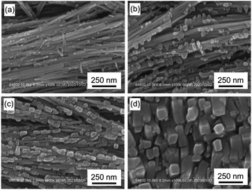 |
| | Fig. 1 SEM images of Cu2(BPDC)2 oriented films synthesized at different reaction times: (a) 30 min, (b) 1 hour, (c) 3 hours, and (d) 24 hours. | |
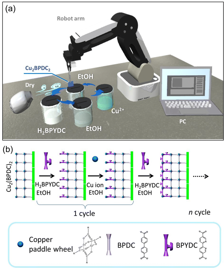
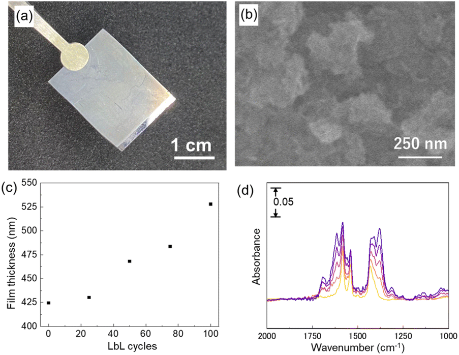
The upper Cu2(BPYDC)2 layer was deposited by the LbL approach, in which the Cu2(BPDC)2 oriented film is alternately immersed in a solution containing Cu2+ ions and a solution containing H2BPYDC linkers (Fig. 2). Washing and drying processes of the film at room temperature were conducted in between immersion processes in the respective solutions. The formation of the MOF film by the LbL approach has been frequently used so far, and more efficient fabrication of large-scale MOF thin films with high reproducibility for industrial applications by automatic processing such as high-throughput spray, large-area spray, spin coating, dipping robot, and flow-based automation, has been developed to replace the manual dipping method.8,41–44 A commercially available robot arm was used to fabricate the upper Cu2(BPYDC)2 layer via the LbL approach in the present study (Fig. 2). Though the process is similar to the method using a dipping robot, the use of a commercially available robot arm provides the capability for anyone to quickly and reproducibly synthesize MOF thin films without the need to design and prepare specialized equipment or special operating techniques. As seen in Fig. 3a, a uniform Cu2(BPYDC)2-on-Cu2(BPDC)2 thin film was fabricated reproducibly by an automated process using a PC-controlled robot arm. The brick-shaped Cu2(BPDC)2 crystals were covered with the Cu2(BPYDC)2 layer without the formation of obviously large Cu2(BPYDC)2 crystals on the thin films, which is in good agreement with the previous report (Fig. 3b).32 This indicates epitaxial growth of Cu2(BPYDC)2 on the surface of Cu2(BPDC)2 as they have essentially identical lattice structures (Fig. S3†).32 The total thickness of the Cu2(BPYDC)2-on-Cu2(BPDC)2 thin film increased linearly (∼1 nm per cycles) with increasing the LbL cycles, indicating successful deposition of the Cu2(BPYDC)2 layer, which is a functional MOF layer for post-metalation (Fig. 3c). The deposition of the Cu2(BPYDC)2 layer was also confirmed by FT-IR investigation. The bands at 1583 cm−1 and 1430 cm−1 observed in the Cu2(BPDC)2 thin film are assigned to the asymmetric and symmetric carboxylate vibration, respectively.45 Additional bands at 1616 cm−1 and 1380 cm−1, which are assigned to C![[double bond, length as m-dash]](https://www.rsc.org/images/entities/char_e001.gif) N and C–N in BPYDC linkers, respectively,46–48 and a steady increase in absorption of those bands were detected with increasing LbL cycles. The steady increase in the growth MOF layer is consistent with the results of reported papers using a LbL approach.49,50 In this study, it was found that a part of the film peels off when the number of LbL cycles exceeds 60. This might be due to the increase in out-of-plane stress caused by the expansion and contraction of the film during the cleaning and drying processes as the film thickness increases. Based on these results, the optimal condition for synthesizing Cu2(BPYDC)2 layers has been determined to be 50 LbL cycles.
N and C–N in BPYDC linkers, respectively,46–48 and a steady increase in absorption of those bands were detected with increasing LbL cycles. The steady increase in the growth MOF layer is consistent with the results of reported papers using a LbL approach.49,50 In this study, it was found that a part of the film peels off when the number of LbL cycles exceeds 60. This might be due to the increase in out-of-plane stress caused by the expansion and contraction of the film during the cleaning and drying processes as the film thickness increases. Based on these results, the optimal condition for synthesizing Cu2(BPYDC)2 layers has been determined to be 50 LbL cycles.
 |
| | Fig. 2 Schematic illustration representing an automated LbL process using a PC-controlled robot arm. (a) The Cu2(BPDC)2 oriented film is alternately immersed in a solution containing Cu2+ ions and H2BPYDC linkers, and the film was washed with ethanol and dried using an electric fan at room temperature in between immersion processes in the respective solutions. (b) A Cu2(BPYDC)2 layer is deposited on Cu2(BPDC)2 with an epitaxial interface in a cycle. | |
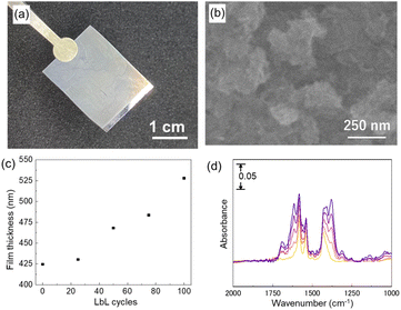 |
| | Fig. 3 (a) A photo and (b) an SEM image of a Cu2(BPYDC)2-on-Cu2(BPDC)2 thin film synthesized after 50 LbL cycles. (c) Total thickness and (d) FT-IR spectra of the Cu2(BPYDC)2-on-Cu2(BPDC)2 thin film as a function of LbL cycles. The thickness is measured with a stylus profilometer. | |
The resulting Cu2(BPYDC)2-on-Cu2(BPDC)2 oriented thin film was immersed in Ag+ ion-containing acetonitrile solution to adsorb Ag+ ions on the chelating bipyridine moiety of BPYDC linkers. The adsorption of Ag+ ions on the Cu2(BPDC)2 layer is low which is insufficient for nanoparticle formation, as reported in our previous work.32 After thoroughly washing off the unadsorbed Ag+ ions, the thin film was exposed to H2 gas (2 MPa) at room temperature to reduce Ag+ to form AgNPs, resulting in the fabrication of an AgNPs@Cu2(BPYDC)2-on-Cu2(BPDC)2 oriented thin film. After AgNP formation, the thin film clearly showed uniform yellowish colour on the entire film surface (Fig. 4a). Obvious AgNP formation on the surface of the thin film was not observed (Fig. 4b). The SEM-EDS mapping images showed that Ag was uniformly distributed throughout the film, indicating that AgNPs were formed inside the film (Fig. 4c–f). Elemental analysis indicated Ag![[thin space (1/6-em)]](https://www.rsc.org/images/entities/char_2009.gif) :N = 1:21.5, which means that 0.09 mol of Ag is present per 1 mol of BPYDC linker. TEM observation revealed that a few nanometer-scale spherical nanoparticles are homogeneously embedded in the MOF film (Fig. S4†). Fig. 5 shows the polarization-dependent UV/Vis absorption spectra measured with an integrated sphere in a reflection mode. Plasmon resonance absorption originating from AgNPs was confirmed at 400–500 nm, which was not observed for the film before AgNP formation. An increase in the intensity of the plasmon resonance absorption was observed when the angle between the a–c plane of the MOF (Cu-paddle wheel sheet) and the light polarization changed from 90° to 0°. The unique anisotropic optical property was discussed as originating from differences in electron–phonon interactions attributed to anisotropy in the thermal conductivity of the oriented MOF lattice surrounding AgNPs.32,51–53
:N = 1:21.5, which means that 0.09 mol of Ag is present per 1 mol of BPYDC linker. TEM observation revealed that a few nanometer-scale spherical nanoparticles are homogeneously embedded in the MOF film (Fig. S4†). Fig. 5 shows the polarization-dependent UV/Vis absorption spectra measured with an integrated sphere in a reflection mode. Plasmon resonance absorption originating from AgNPs was confirmed at 400–500 nm, which was not observed for the film before AgNP formation. An increase in the intensity of the plasmon resonance absorption was observed when the angle between the a–c plane of the MOF (Cu-paddle wheel sheet) and the light polarization changed from 90° to 0°. The unique anisotropic optical property was discussed as originating from differences in electron–phonon interactions attributed to anisotropy in the thermal conductivity of the oriented MOF lattice surrounding AgNPs.32,51–53
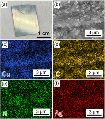 |
| | Fig. 4 (a) A photo of the AgNPs@Cu2(BPYDC)2-on-Cu2(BPDC)2 thin film. (b) SEM and (c–f) EDS mapping images of the AgNPs@Cu2(BPYDC)2-on-Cu2(BPDC)2 thin film. | |
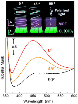 |
| | Fig. 5 Polarization-dependent UV/Vis reflection spectra of the AgNPs@Cu2(BPYDC)2-on-Cu2(BPDC)2 thin film. Angles in the figure show the angles between the a–c plane of the MOF crystal and the electric field component of polarization of the light as described in the image above. | |
Plasmonic metal nanoparticles have been intensively employed in a broad range of applications in the fields of biomedical, energy, and information technology due to their unique optical properties arising from their interactions with incident light.54,55 In addition to the unique optical properties, plasmonic nanoparticles efficiently and quickly convert light into heat, which leads to lattice heating, heating of the environment and the generation of hot electrons. Recently, a stream of temperature-related phenomena induced by plasmonic absorption has attracted significant attention for nonlinear optics, hot electrons for renewable energy (e.g., solar cells and water-splitting), acousto-optics, nanometalworking, nanorobotics, steam generation, and photothermal cancer therapy.56 Integrating the temperature-related phenomena induced by plasmonic absorption into MOF thin films has the potential to generate MOF thin film-based materials for these applications. The unique polarization-dependent plasmon resonance absorption that we found in the AgNPs@Cu2(BPYDC)2-on-Cu2(BPDC)2 oriented film is expected to afford polarization-dependent plasmonic heating of the MOF film as plasmon resonance absorption in metal nanoparticles is closely related to plasmonic heating. Due to the large polarization-dependent plasmon damping in the MOF oriented thin film, it is expected that the plasmon heating temperature can be modulated simply by changing the angle between the MOF crystallographic axis and the electric field component of polarization of the light when the MOF thin film is irradiated with a polarized laser. Accordingly, in this study, we irradiated the AgNPs@Cu2(BPYDC)2-on-Cu2(BPDC)2 oriented film with a laser (λ = 440 nm) through a polarizer, of which wavelength corresponds to the plasmon-resonance absorption of the AgNPs, and the temperature of the film was monitored in the experimental setup shown in Fig. 6a. The MOF thin film was prepared on a Si substrate, and the temperature of the substrate was monitored directly from the backside using thermocouples. In the case of the configuration of the weakest plasmon resonance absorption (90°) where the a–c plane of the Cu2(BPYDC)2-on-Cu2(BPDC)2 oriented film was perpendicular to the electric field component of polarization of the light, the sample temperature increased with increasing irradiation time and reached ca. 45 °C after 180 seconds of irradiation (Fig. 6b). When the same sample was rotated 90° (the configuration of the largest plasmon resonance absorption (0°)), the sample temperature reached ca. 50 °C after 180 seconds of irradiation. It was found that a temperature difference of approximately 5 °C could be achieved by simply changing the angle between the MOF crystallographic axis and the electric field component of polarized light. The unique polarization-dependent plasmonic heating was not observed in a randomly oriented AgNPs@Cu2(BPYDC)2-on-Cu2(BPDC)2 thin film (Fig. 6c and S5†). It should be mentioned that reproducibility of the polarization-dependent plasmonic heating behavior of the AgNP-incorporated MOF oriented thin films was experimentally confirmed, although the attained temperatures were varied with samples in several degrees due to the differences of measurement conditions such as surrounding temperature, substrate size, contacts between the sample and a thermocouple and others. Another factor which should be considered is the anisotropic heat transport in the in-plane direction of the oriented MOF film (higher thermal conductivity along b axis). However, this can be ruled out because the MOFs are not heated directly with laser light whose wavelength is inconsistent with the absorption wavelength of the MOFs. Therefore, the polarization-dependent plasmon heating can be explained by the difference in plasmonic heating originating from polarization-dependent plasmon-resonance of AgNPs embedded as a point heat source in the MOF oriented thin film. Hence, this is a novel anisotropic optical property in a MOF thin film that can only be attained with AgNP-incorporated MOF oriented thin films in which the MOF crystals are oriented in all three axes over a large area (at least larger than the laser spot). Although the integration of plasmonic nanoparticles with the MOF has been demonstrated to improve the photocatalytic activities of the MOF,57–59 this is the first report showing polarization-dependent plasmonic heating in the MOF field. This result was achieved by the integration of plasmonic nanoparticles into a thin film of MOF crystals oriented over a large area. The MOF thin film with unique temperature-related phenomena induced by plasmonic absorption will open up new possibilities for applications since heating can be triggered and controlled by external irradiation, for instance, with a laser. For example, local heating of MOF thin films with a laser is expected for efficient reactivation (photothermal induced desorption of adsorbed gases) in MOF thin film sensors and MOF-based adsorbent sheets, and for the improvement of efficiency in the MOF catalytic film and the MOF film for steam generation. Moreover, the utilization of such MOF thin films showing polarization-dependent plasmonic heating will pave the way for new possible applications such as soft nanorobotics in composites with thermo-responsive materials.
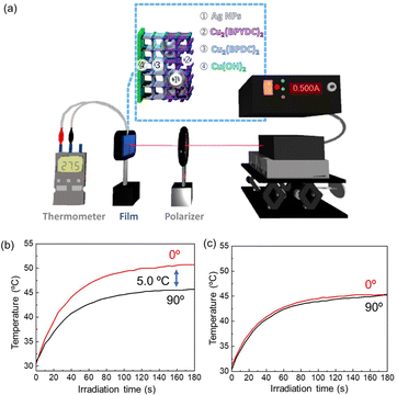 |
| | Fig. 6 (a) An experimental setup for the polarization-dependent plasmonic heating of the AgNPs@Cu2(BPYDC)2-on-Cu2(BPDC)2 oriented film. Sample temperature as a function of laser irradiation time for (b) the oriented thin film and (c) the randomly oriented thin film. | |
Conclusions
Epitaxially grown multilayered metal–organic framework thin films embedded with Ag nanoparticles have been prepared in three steps with optimized synthesis conditions. Epitaxial growth of Cu2(BPDC)2 crystals on Cu(OH)2 nanobelts for 24 hours in the first step leads to the fabrication of highly oriented Cu2(BPDC)2 thin films completely covering the Cu(OH)2 nanobelt surface. An automated layer-by-layer approach using a robot arm in the second step enables the formation of uniform MOF-on-MOF thin films after 50 layer-by-layer cycles where the surface of Cu2(BPDC)2 crystals is covered with a Cu2(BPYDC)2 layer. The uniform formation of the MOF-on-MOF oriented film allows the uniform incorporation of silver nanoparticles into the upper Cu2(BPYDC)2 layer in the third step. The silver nanoparticles embedded in the MOF-on-MOF oriented film exhibit polarization-dependent plasmon resonance absorption. A MOF thin film with a polarization-dependent plasmonic heating behavior is achieved thanks to the difference in polarization-dependent plasmon-resonance absorption. Such MOF thin films can be heated at different locations with lasers, paving the way for applications such as efficient reactivation in MOF thin film sensors, partial catalytic reactions in MOF thin film devices, and soft nanorobotics in composites with thermo-responsive materials.
Author contributions
K. O.: design of methodology, curation, resources, writing – original draft; R. M.: MOF synthesis, validation; A. F.: validation, writing – review & editing; M. T.: design of methodology, validation, resources, writing – review & editing, funding acquisition.
Conflicts of interest
There are no conflicts to declare.
Acknowledgements
The present work is partially supported by Grand-in-Aids from the Ministry of Education, Culture, Sports, Science and Technology (MEXT), administrated by Japan Society for the Promotion of Science (JSPS) (JP20H00401, JP22H05144 and JP22H05142), and also by JST, PRESTO Grant Number JPMJPR19I3, Japan.
References
- H. Furukawa, K. E. Cordova, M. O'Keeffe and O. M. Yaghi, Science, 2013, 341, 1230444 CrossRef PubMed.
- S. Kitagawa, R. Kitaura and S.-I. Noro, Angew. Chem., Int. Ed., 2004, 43, 2334–2375 CrossRef CAS PubMed.
- J. Lee, O. K. Farha, J. Roberts, K. A. Scheidt, S. T. Nguyen and J. T. Hupp, Chem. Soc. Rev., 2009, 38, 1450 RSC.
- D. Yang and B. C. Gates, ACS Catal., 2019, 9, 1779–1798 CrossRef CAS.
- K. Adil, Y. Belmabkhout, R. S. Pillai, A. Cadiau, P. M. Bhatt, A. H. Assen, G. Maurin and M. Eddaoudi, Chem. Soc. Rev., 2017, 46, 3402–3430 RSC.
- K. Sumida, D. L. Rogow, J. A. Mason, T. M. Mcdonald, E. D. Bloch, Z. R. Herm, T.-H. Bae and J. R. Long, Chem. Rev., 2012, 112, 724–781 CrossRef CAS PubMed.
- O. Shekhah, J. Liu, R. a. Fischer and C. Wöll, Chem. Soc. Rev., 2011, 40, 1081–1106 RSC.
- J. Liu and C. Woll, Chem. Soc. Rev., 2017, 46, 5730–5770 RSC.
- K. Okada, S. Sawai, K. Ikigaki, Y. Tokudome, P. Falcaro and M. Takahashi, CrystEngComm, 2017, 19, 4194–4200 RSC.
- T. Toyao, K. Liang, K. Okada, R. Ricco, M. J. Styles, Y. Tokudome, Y. Horiuchi, A. J. Hill, M. Takahashi, M. Matsuoka and P. Falcaro, Inorg. Chem. Front., 2015, 2, 434–441 RSC.
- K. Okada, R. Ricco, Y. Tokudome, M. J. Styles, A. J. Hill, M. Takahashi and P. Falcaro, Adv. Funct. Mater., 2014, 24, 1969–1977 CrossRef CAS.
- M. Tu, B. Xia, D. E. Kravchenko, M. L. Tietze, A. J. Cruz, I. Stassen, T. Hauffman, J. Teyssandier, S. De Feyter, Z. Wang, R. A. Fischer, B. Marmiroli, H. Amenitsch, A. Torvisco, M. D. J. Velásquez-Hernández, P. Falcaro and R. Ameloot, Nat. Mater., 2021, 20, 93–99 CrossRef CAS PubMed.
- K. Ikigaki, K. Okada, Y. Tokudome and M. Takahashi, J. Sol-Gel Sci. Technol., 2018, 89, 128–134 CrossRef.
- M. Krishtab, I. Stassen, T. Stassin, A. J. Cruz, O. O. Okudur, S. Armini, C. Wilson, S. De Gendt and R. Ameloot, Nat. Commun., 2019, 10, 3729 CrossRef PubMed.
- I. Stassen, M. Styles, G. Grenci, H. Van Gorp, W. Vanderlinden, S. De Feyter, P. Falcaro, D. De Vos, P. Vereecken and R. Ameloot, Nat. Mater., 2016, 15, 304–310 CrossRef CAS PubMed.
- I. Stassen, N. Burtch, A. Talin, P. Falcaro, M. Allendorf and R. Ameloot, Chem. Soc. Rev., 2017, 46, 3185–3241 RSC.
- L. S. Xie, G. Skorupskii and M. Dincă, Chem. Rev., 2020, 120, 8536–8580 CrossRef CAS PubMed.
- L. Sun, M. G. Campbell and M. Dincă, Angew. Chem., Int. Ed., 2016, 55, 3566–3579 CrossRef CAS PubMed.
- C. A. Downes and S. C. Marinescu, ChemSusChem, 2017, 10, 4374–4392 CrossRef CAS PubMed.
- G. Givaja, P. Amo-Ochoa, C. J. Gómez-García and F. Zamora, Chem. Soc. Rev., 2012, 41, 115–147 RSC.
- L. Sun, S. S. Park, D. Sheberla and M. Dincă, J. Am. Chem. Soc., 2016, 138, 14772–14782 CrossRef CAS PubMed.
- K. Allahyarli, M. R. Reithofer, F. Cheng, A. J. Young, E. Kiss, T. T. Y. Tan, A. Prado-Roller and J. M. Chin, J. Colloid Interface Sci., 2022, 610, 1027–1034 CrossRef CAS PubMed.
- P. I. Scheurle, A. Mähringer, A. Biewald, A. Hartschuh, T. Bein and D. D. Medina, Chem. Mater., 2021, 33, 5896–5904 CrossRef CAS.
- L.-A. Cao, M.-S. Yao, H.-J. Jiang, S. Kitagawa, X.-L. Ye, W.-H. Li and G. Xu, J. Mater. Chem. A, 2020, 8, 9085–9090 RSC.
- X. Mu, W. Wang, C. Sun, J. Wang, C. Wang and M. Knez, Adv. Mater. Interfaces, 2021, 8, 2002151 CrossRef CAS.
- Y. Lin, W. H. Li, Y. Wen, G. E. Wang, X. L. Ye and G. Xu, Angew. Chem., Int. Ed., 2021, 60, 25758–25761 CrossRef CAS PubMed.
- Z.-Z. Ma, Q.-H. Li, Z. Wang, Z.-G. Gu and J. Zhang, Nat. Commun., 2022, 13, 6347 CrossRef CAS PubMed.
- K. Okada, K. Mori, A. Fukatsu and M. Takahashi, J. Mater. Chem. A, 2021, 9, 19613–19618 RSC.
- K. Okada, M. Nakanishi, K. Ikigaki, Y. Tokudome, P. Falcaro, C. J. Doonan and M. Takahashi, Chem. Sci., 2020, 11, 8005–8012 RSC.
- K. Ikigaki, K. Okada and M. Takahashi, ACS Appl. Nano Mater., 2021, 4, 3467–3475 CrossRef CAS.
- P. Falcaro, K. Okada, T. Hara, K. Ikigaki, Y. Tokudome, A. W. Thornton, A. J. Hill, T. Williams, C. Doonan and M. Takahashi, Nat. Mater., 2017, 16, 342–348 CrossRef CAS PubMed.
- K. Ikigaki, K. Okada, Y. Tokudome, T. Toyao, P. Falcaro, C. J. Doonan and M. Takahashi, Angew. Chem., Int. Ed., 2019, 58, 6886–6890 CrossRef CAS PubMed.
- B. Baumgartner, R. Mashita, A. Fukatsu, K. Okada and M. Takahashi, Angew. Chem., Int. Ed., 2022, 61, e202201725 CrossRef CAS PubMed.
- M. D. Allendorf, A. Schwartzberg, V. Stavila and A. A. Talin, Chem, 2011, 17, 11372–11388 CrossRef CAS PubMed.
- P. Falcaro, D. Buso, A. J. Hill and C. M. Doherty, Adv. Mater., 2012, 24, 3153–3168 CrossRef CAS PubMed.
- P. Falcaro, R. Ricco, C. M. Doherty, K. Liang, A. J. Hill and M. J. Styles, Chem. Soc. Rev., 2014, 43, 5513–5560 RSC.
- M. Linares-Moreau, L. A. Brandner, T. Kamencek, S. Klokic, F. Carraro, K. Okada, M. Takahashi, E. Zojer, C. J. Doonan and P. Falcaro, Adv. Mater. Interfaces, 2021, 8, 2101039 CrossRef CAS.
- P. Falcaro, R. Ricco, A. Yazdi, I. Imaz, S. Furukawa, D. Maspoch, R. Ameloot, J. D. Evans and C. J. Doonan, Coord. Chem. Rev., 2016, 307, 237–254 CrossRef CAS.
- J. D. Evans, C. J. Sumby and C. J. Doonan, Chem. Soc. Rev., 2014, 43, 5933–5951 RSC.
- E. D. Bloch, D. Britt, C. Lee, C. J. Doonan, F. J. Uribe-Romo, H. Furukawa, J. R. Long and O. M. Yaghi, J. Am. Chem. Soc., 2010, 132, 14382–14384 CrossRef CAS PubMed.
- V. Chernikova, O. Shekhah and M. Eddaoudi, ACS Appl. Mater. Interfaces, 2016, 8, 20459–20464 CrossRef CAS PubMed.
- F. Maya, C. Palomino Cabello, S. Clavijo, J. M. Estela, V. Cerdà and G. Turnes Palomino, Chem. Commun., 2015, 51, 8169–8172 RSC.
- H. K. Arslan, O. Shekhah, J. Wohlgemuth, M. Franzreb, R. A. Fischer and C. Wöll, Adv. Funct. Mater., 2011, 21, 4228–4231 CrossRef CAS.
- Z.-G. Gu, A. Pfriem, S. Hamsch, H. Breitwieser, J. Wohlgemuth, L. Heinke, H. Gliemann and C. Wöll, Microporous Mesoporous Mater., 2015, 211, 82–87 CrossRef CAS.
- B. Baumgartner, K. Ikigaki, K. Okada and M. Takahashi, Chem. Sci., 2021, 12, 9298–9308 RSC.
- B. Mortada, T. A. Matar, A. Sakaya, H. Atallah, Z. Kara Ali, P. Karam and M. Hmadeh, Inorg. Chem., 2017, 56, 4739–4744 CrossRef PubMed.
- Y. Li, H. Liu, W.-J. Li, F.-Y. Zhao and W.-J. Ruan, RSC Adv., 2016, 6, 6756–6760 RSC.
- Y. Zhou, J. Liu and J. Long, J. Solid State Chem., 2021, 303, 122510 CrossRef CAS.
- Z. Wang and C. Wöll, Adv. Mater. Technol., 2019, 4, 1800413 CrossRef.
- A. Summerfield, I. Cebula, M. Schröder and P. H. Beton, J. Phys. Chem. C, 2015, 119, 23544–23551 CrossRef CAS PubMed.
- S. Wieser, T. Kamencek, R. Schmid, N. Bedoya-Martínez and E. Zojer, Nanomaterials, 2022, 12, 2142 CrossRef CAS PubMed.
- X. Wang, R. Guo, D. Xu, J. Chung, M. Kaviany and B. Huang, J. Phys. Chem. C, 2015, 119, 26000–26008 CrossRef CAS.
- T. G. Habteyes, S. Dhuey, E. Wood, D. Gargas, S. Cabrini, P. J. Schuck, A. P. Alivisatos and S. R. Leone, ACS Nano, 2012, 6, 5702–5709 CrossRef CAS PubMed.
- L. Jauffred, A. Samadi, H. Klingberg, P. M. Bendix and L. B. Oddershede, Chem. Rev., 2019, 119, 8087–8130 CrossRef CAS PubMed.
- L. Wang, M. Hasanzadeh Kafshgari and M. Meunier, Adv. Funct. Mater., 2020, 30, 2005400 CrossRef CAS.
- C. Kuppe, K. R. Rusimova, L. Ohnoutek, D. Slavov and V. K. Valev, Adv. Opt. Mater., 2019, 8, 1901166 CrossRef.
- M. Wang, Y. Tang and Y. Jin, ACS Catal., 2019, 9, 11502–11514 CrossRef CAS.
- W.-C. Hu, Y. Shi, Y. Zhou, C. Wang, M. R. Younis, J. Pang, C. Wang and X.-H. Xia, J. Mater. Chem. A, 2019, 7, 10601–10609 RSC.
- Q. Yang, Q. Xu, S.-H. Yu and H.-L. Jiang, Angew. Chem., Int. Ed., 2016, 55, 3685–3689 CrossRef CAS PubMed.
|
| This journal is © The Royal Society of Chemistry 2023 |

 Open Access Article
 This Open Access Article is licensed under a Creative Commons Attribution-Non Commercial 3.0 Unported Licence
 *ab,
Risa
Mashita
c,
Arisa
Fukatsu
*ab,
Risa
Mashita
c,
Arisa
Fukatsu