
 Open Access Article
 This Open Access Article is licensed under a Creative Commons Attribution-Non Commercial 3.0 Unported Licence
High-efficiency and high-resolution patterned quantum dot light emitting diodes by electrohydrodynamic printing†
Haowei
Wang
,
Yuanming
Zhang
,
Yang
Liu
,
Zhuo
Chen
 *,
Yanzhao
Li
*,
Xinguo
Li
and
Xiaoguang
Xu
*,
Yanzhao
Li
*,
Xinguo
Li
and
Xiaoguang
Xu
BOE Technology Group Co., Ltd., No. 9 Dize Road, Beijing 100176, China. E-mail: chenzhuo_cto@boe.com.cn
First published on 30th January 2023
Abstract
The development of quantum dot light-emitting diode (QLED) fabrication technologies for high-definition and low-cost displays is an important research topic. However, commercially available piezoelectric inkjet printing has reached its limit in reducing pixel sizes, which restricts its potential use in high-resolution displays. Here, we exhibit an electrohydrodynamic (EHD) printing method for manufacturing QLEDs with a high resolution of 500 ppi that remarkably surpasses the resolution of conventional inkjet printing displays. By optimizing the EHD printing process, a high-resolution pixelated bottom-emitting passive matrix QLED with a maximal current efficiency of 14.4 cd A−1 in a pixel size of 5 μm × 39 μm was achieved, indicating the capability of the EHD method in superfine printing and high efficiency QLED. Moreover, a top-emitting device is designed using a capping layer; the maximal current efficiency of top-emission passive matrix QLED devices can reach up to 16.5 cd A−1. Finally, a two-color (red and green) bottom-emission QLED device with 500 ppi was fabricated. The successful fabrication of these high-efficiency QLEDs with 500 ppi demonstrated that the EHD printing strategy has numerous potential applications in high-resolution and high-performance QLEDs for a range of applications, such as mobile or wearable devices.
Introduction
Quantum dots (QDs) have attracted considerable attention because of their outstanding properties, such as adjustable band gap,1 narrow full width at half maximum2 and easy synthesis.3 Among all QD applications, QD light emitting diode (QLED) is an advancing technology.4–6 QLED can meet people's demand for high-performance displays, such as wide color gamut, low power consumption and high stability, and significantly reduce manufacturing costs.7,8 Therefore, as an important competitor in the next generation of display technology, QLED has attracted considerable attention and undergone rapid development in QD materials, device mechanisms, device architectures and fabrication technologies.9–11For display applications, the patterning of luminescent materials is an essential process. At present, mature and commercial OLEDs are patterned by fine metal mask (FMM).12,13 This makes OLED expensive to manufacture owing to the need for a vacuum environment, the high manufacturing cost of FMM and the waste of many evaporation materials. Compared with the costly and complex FMM vacuum-patterning method used in OLED,12,13 QLED devices via inkjet printing in ambient conditions are significantly simpler and cost-saving.14–16 However, traditional inkjet printing with a minimum printing line width of 20 μm can only satisfy the manufacturing demand of large-size displays with a pixel density of about 220 pixels per inch (ppi), which means that it is unachievable to fabricate mobile phone displays with higher resolution of over 400 ppi.17
Different from the traditional piezoelectric inkjet printing method, the electric field around the nozzle is very vital in the process of electrohydrodynamic (EHD) printing.18,19 Because the electric field forces can “pull” the ink out of the nozzle rather than “squeeze” it, it possesses the ability to print with high resolution that can satisfy the application in small and medium size displays.20–23 In the last few years, numerous developers have paid close attention to the EHD printing technology to fabricate photoelectric device.24,25 In 2015, Kim et al. reported a printing strategy of red and green QDs in a multilayer architecture to pattern the array of dots and lines; then, they used a substrate with no pixel definition layer (PDL) to fabricate patterned QLED. The maximum external quantum efficiency (EQE) can reach up to 2.6%.26 In 2020, Li et al. fabricated an inverted 306 ppi pixelated QLED using EHD printing technology, and the maximum EQE of QLED can reach 0.55%.27 However, there are few reports about QLED devices prepared by the EHD printing method, and their performance is relatively poor at present. Further enhancement in the efficiency of EHD printing QLED devices would enable them to be competitive with those of other alternative display technologies. Insignificant research has been conducted on the effects of QD ink during EHD printing because of the presence of a large electric field. Consequently, we report an EHD printing method for fabricating QLED with a high resolution of 500 ppi, and the effect of a high electric field during EHD printing on QD ink was also investigated. Furthermore, the effect of various viscosity inks on print linewidth has been studied, proving that print linewidth can be regulated finer by ink viscosity. The formation of the QLED pixel's width of 5 μm significantly exceeds that of conventional inkjet-printed pixels. By optimizing the thickness of the QD film in pixels through printing speed, the bottom emission with a high current efficiency of 14.4 cd A−1 was successfully fabricated. Moreover, because top emission QLED devices are unaffected by whether the substrate is transparent or not, the top emitting QLED can effectively improve the aperture ratio of the display panel, expand the design of the thin film transistor (TFT) circuit on the substrate, enrich the choice of electrode materials, and facilitate the integration of the device and TFT circuit. Therefore, compared with the bottom emitting device, the top emitting device architecture has a broader application prospect.28 Furthermore, in the top emission architecture, the forward direction emission of the device can be adjusted by the micro-cavity effect and capping layer (CPL), which is good for mobile and AR/VR displays.29–32 Finally, the top-emission PM QLED devices with 500 ppi were fabricated, and the current efficiency can reach up to 16.5 cd A−1. Bottom- and top-emission QLED devices fabricated using the EHD printing method are prospective for next-generation displays with high pixel density.
Materials and experimental
The red QD ink was purchased from Suzhou Xingshuo Nanotech Co., Ltd. Zinc oxide nanoparticle solution (ZnO NP) was manufactured by Poly OptoElectronics Tech. Ltd. 4,4′,4′′-Tris(carbazol-9-yl)-triphenylamine (TCTA), N,N′-bis-(1-naphthalenyl)-N,N′-bis-phenyl-(1,1′-biphenyl)-4,4′-diamine (NPB) and hexaazatriphenylenehexacabonitrile (HAT-CN) were purchased from J&K Scientific. Silver (99.99%) and magnesium (99.99%) evaporation materials were purchased from CNM, Inc. Other solvents used were all super dry grade obtained from Shanghai Titan Tech. Ltd.The substrates were cleaned in deionized water, acetone and ethyl alcohol for 15 min and then treated with UV–ozone for 10 min. Subsequently, an electron transport layer (ETL) of ZnO nanoparticles was spin-coated on the substrate for 40 s and then annealed at 120 °C for 20 min in an N2 filled glove box. Next, red QDs ink (30 mg ml−1) was deposited on the substrates by an EHD system. The thickness of the QDs was adjusted by changing the printing speed. After the deposition of the solution-processed layers, all samples were transferred to a vacuum deposition chamber with chamber pressure below 10−6 torr. TCTA, NPB and HAT-CN, Ag and Ag![[thin space (1/6-em)]](https://www.rsc.org/images/entities/char_2009.gif) :Mg with various thicknesses were deposited consequentially in a vacuum chamber, followed by encapsulation with a UV-curable epoxy and cover glasses in N2 atmosphere. The Ag and Ag:Mg (with an Mg doping ratio of 20%) thicknesses were 120 nm and 10 nm in the bottom- and top-emission devices, respectively. For top emission devices, a 60 nm capping layer was deposited on an Ag:Mg electrode. The organic materials and electrode thickness were controlled using the quartz crystal oscillator with a deposition rate of 0.5–1 Å s−1.
:Mg with various thicknesses were deposited consequentially in a vacuum chamber, followed by encapsulation with a UV-curable epoxy and cover glasses in N2 atmosphere. The Ag and Ag:Mg (with an Mg doping ratio of 20%) thicknesses were 120 nm and 10 nm in the bottom- and top-emission devices, respectively. For top emission devices, a 60 nm capping layer was deposited on an Ag:Mg electrode. The organic materials and electrode thickness were controlled using the quartz crystal oscillator with a deposition rate of 0.5–1 Å s−1.
Results and discussion
Fig. 1a shows a schematic illustration of the EHD printing system, including a single nozzle, a movable platform, a conductive platform and a power supply system. When a voltage bias is applied to the nozzle, the QD ink can be ejected from the tip of the nozzle. Line patterns can be printed by operating the EHD system with the programmed movable platform. We accurately controlled the print line width by changing the printing speed and ink viscosity. Fig. 1b depicts the line widths of inks with viscosities of 6 cP, 10 cP and 20 cP at various printing speeds. We can conclude that increasing the printing speed can reduce the line width and that QD ink with high viscosity has a narrower line width under the same printing conditions compared with low viscosity QDs ink. Fig. 1c–g shows the fluorescence images of QD inks with a viscosity of 6 cP at various printing speeds. The printed lines show smooth edges with a line width of 18.1 μm, 13.1 μm, 9.7 μm, 6.7 μm and 2.6 μm. The fluorescence images of QDS inks with viscosities of 10 cP and 20 cP are shown in Fig. S2.† Based on these results, the linewidth can also be regulated and controlled by the voltage magnitude, as shown in Fig. S1.† The specific print parameters and line widths with different printing speeds and ink viscosity are summarized in Table S1.†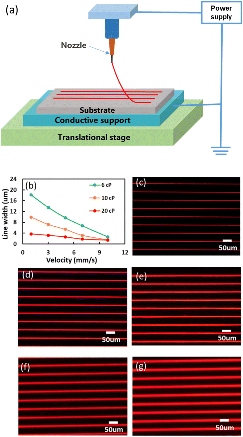 | ||
| Fig. 1 (a) Schematic illustration of the EHD printing system comprising a single nozzle, a movable platform, a conductive platform and a power supply system, (b) and (c–g) fluorescence images of patterned lines with QD ink of 6 cP at printing speeds of 10 mm s−1, 7 mm s−1, 5 mm s−1, 3 mm s−1 and 1 mm s−1, respectively. | ||
As we all know, QDs comprise core/shell and ligands. The organic ligands are bonded to the inorganic core–shell architectures by chemical coordination bonds. For the sake of exploring the possible effects of the high electric field on QD ink in the printing process, we investigated the QD ink with and without an EHD printing system by UV-Vis spectroscopy, photoluminescence (PL) spectrum and the photo-luminescence quantum yield (PLQY) of QD ink. As shown in Fig. 2, the UV-Vis spectroscopy, PL spectrum and PLQY of QD ink were almost similar with and without the EHD printing system. Furthermore, the time-resolved fluorescence spectroscopy (TRPL) and ultraviolet photoelectron spectroscopy (UPS) of the QD film with and without the EHD printing system were also unchanged, as shown in Fig. S3.† The relevant data showed that the high electric field of the EHD system had no side effect on the QD ink.
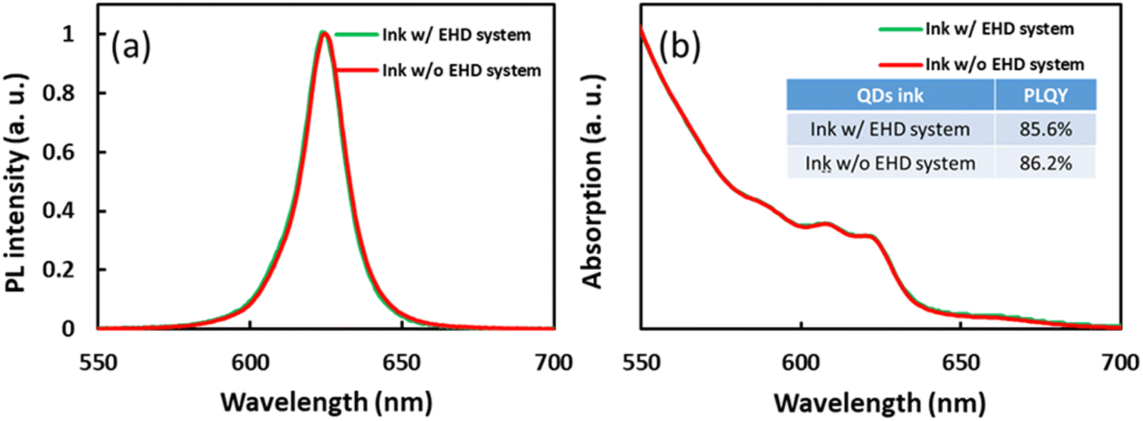 | ||
| Fig. 2 (a) The photoluminescence spectrum of QD ink with and without the EHD system, (b) the UV-Vis spectrum of QD ink with and without the EHD system, and the inset table shows the PLQY of QD ink with and without the EHD system. | ||
In practice, red QD ink should be ejected into the pixels of the PM substrate, and we accordingly prepared a pixel definition layer (PDL) on indium tin oxide (ITO) strips using a commercial photoresist. As shown in Fig. S4a,† pixels in the size of 5 μm × 39 μm with a pixel pitch of 12 μm were defined by PDL, which has a good insulating property to reduce the short circuit of QLED devices and define the size and shape of each pixel. To achieve high-resolution QLED devices, ink droplets must be accurately printed into pixels that were defined by the photolithography process. Fig. S4b† illustrates the photoluminescence of a PM substrate with pixel architecture printed using QDs ink, and the QD ink was printed into the pixel in exactly every three lines. The uniformity and surface morphology of a printed QD emitting layer is important for the performance of QLED devices. Fig. S4(c–e)† shows atomic force microscope (AFM) images of ITO, ITO/ZnO and ITO/ZnO/QDs surfaces in an area of 4 μm × 4 μm at the bottom of the pixel. The root mean square (RMS) roughness of ITO, ITO/ZnO and ITO/ZnO/QDs surface were 0.15 nm, 0.73 nm and 1.72 nm, respectively. As shown in Fig. 3e, the EHD printing system can print a flatter film with a constant thickness, which results in better device performance.
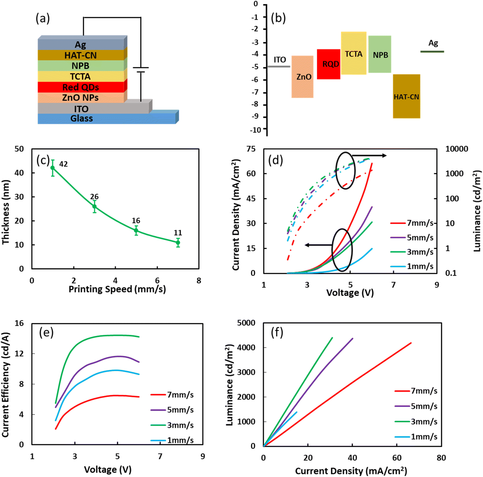 | ||
| Fig. 3 (a) Schematic device architecture and (b) energy level alignment of PM bottom-emission QLED devices, (c) the thickness of the QD layer in the pixel at different printing speeds, (d) J–V–L characteristics, (e) current efficiency–voltage curves and (f) luminance–current density curves of QLEDs with various printing speeds. | ||
To achieve pixelated QLED devices with a high-resolution integrated EHD printing system, an inverted architecture with bottom-emitting QLEDs is demonstrated in Fig. 3a, comprising glass/ITO/ZnO NPs/QDs/TCTA/NPB/HAT-CN/Ag layers. The corresponding energy band diagrams are shown in Fig. 3b. ZnO nanoparticles were used as the ETL because of their efficient electron transfer and injection capabilities. The HAT-CN was chosen as the hole injection layer HIL. The hole transport layers (HTLs) were TCTA and NPB because the highest occupied molecular orbital (HOMO) energy levels of TCTA and red QDs were very close, and NPB had higher carrier mobility for hole transport. The red QD emitting layer was printed using the EHD system with careful alignment to fill the corresponding pixelated substrate.
The thickness of the quantum dot layer significantly affects QLED device performance. To obtain the optimal thickness of the emitting layer, we adjusted the emitting layer thickness by controlling the printing speed of the QD ink. As shown in Fig. 3c, the thicknesses of the QD film layer with velocities of 7 mm s−1, 5 mm s−1, 3 mm s−1 and 1 mm s−1 were 11.2 nm, 16.1 nm, 26.1 nm and 42.6 nm. As the printing speed increased, the thickness of the QD film gradually decreased, and the specific test data measured by the stylus profiler are shown in Fig. S5.† The current density–voltage, luminance–voltage, current efficiency–voltage and luminance–current density characteristics of these QLED devices with various printing speeds are shown in Fig. 3d–f. As shown in Fig. 3c, the current density increased with a higher printing speed, which can contribute to the decreased thickness of the QD film. In addition, Fig. 3d shows that there is an insignificant change in luminance at various printing speeds of 7 mm s−1, 5 mm s−1 and 3 mm s−1; however, the current density changed significantly. When we further lowered the printing speed to 1 mm s−1, both the luminance and current density decreased simultaneously, which led to decreased current efficiency when compared with that of QLEDs at 5 mm s−1 and 3 mm s−1 printing speeds. The quantum dot layer thickness of the device with a printing speed of 3 mm s−1 agrees with that of the spin-coating QLED device with the best performance around 26 nm; then, a maximal current efficiency of 14.4 cd A−1 was achieved. When the printing speed was larger than 3 mm s−1, the quantum dot layer was relatively thin, which may lead to the leakage channel of the QLED device, and the current increased, thus leading to a decrease in QLED device performance. The operational lifetime of the device with a printing speed of 3 mm s−1 and the EQE–voltage characteristics of these QLED devices with different printing speeds are shown in Fig. S6.† When the printing speed was less than 3 mm s−1, the thicker quantum dot film increased the difficulty of carrier recombination and also led to the deterioration of QLED device performance.
After optimizing the performance of the bottom emission QLED, the top emission architecture, in which light can be emitted through the transparent or semitransparent, was introduced owing to the high aperture ratios, efficient light out-coupling and easy control of micro-cavity phenomena. We adopted a bottom electrode (ITO/Ag/ITO) and a top semitransparent cathode fabricated by the co-evaporation of a 10 nm-thick Ag:Mg electrode with a 20% Mg doping ratio. As shown in Fig. 4a, the device was glass/ITO/Ag/ITO/ZnO/QDs/TCTA/NPB/HAT-CN/semi-transparent cathode/CPL. As shown in Fig. 4b, the red and green solid lines represent the electroluminescence angular distribution spectrum of the top and bottom emission devices that were fabricated, respectively. The solid black line represents the Lambert distribution. We can conclude that the electroluminescence angular distribution of the bottom emission devices was similar to the Lambert distribution and that the top emission device was good for light emission from the normal direction. Hence, as shown in Fig. 4c, the current efficiency of the top emission device was better than that of the bottom emission device, which increased from 14.4 cd A−1 to 16.5 cd A−1. Fig. 4d shows the normalized electroluminescence spectrum of the top and bottom emission devices at a voltage of 5 V. As we can see, the electroluminescence peak width at half the height of the top emission device was significantly narrower than that of the bottom emission device, which decreased from 30 nm to 24 nm. This phenomenon was beneficial owing to the micro-cavity formation between the semi-transparent electrode and the Ag/ITO/Ag electrode in the top emission QLED devices. The performance improvement in current efficiency and FWHM indicated that the top emission architecture is beneficial to its application in mobile or AR/VR displays.
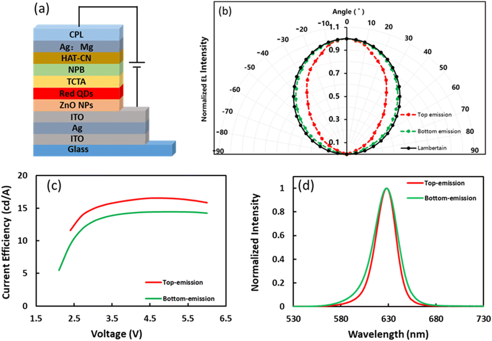 | ||
| Fig. 4 (a) Schematic device architecture of PM top-emission QLED devices, (b) normalized angular-dependent EL intensity, (c) current efficiency curves and (d) comparison of the normalized electroluminescent spectra of the bottom and top emission QLEDs. | ||
Furthermore, a two-colour (red and green) PM-based bottom-emission QLED device with 500 ppi was fabricated using the EHD printing system and magnified photoluminescence images from the red and green sub-pixels, as demonstrated in Fig. 5a. The current density–voltage–luminance (J–V–L) characteristics of the two-color bottom-emission QLED devices are shown in Fig. S7.† The EL spectra of red and green color emissions are demonstrated in Fig. 5b, and the EL emission spectra of red and green sub-pixels were 628 nm and 525 nm, respectively. Fig. 5c and d show the photo and magnified electroluminescence images of red and green sub-pixels, respectively, when lightening up simultaneously. The electroluminescence images of the red and green sub-pixels that were lighted up separately are shown in Fig. S8.†
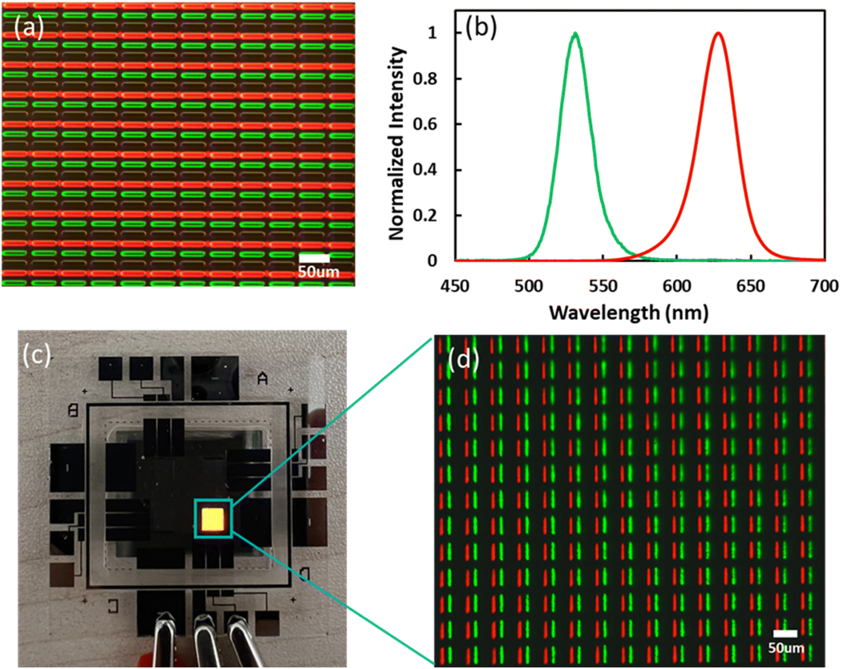 | ||
| Fig. 5 (a) Magnified photoluminescence images of the two-color (red and green) bottom-emission QLED devices, (b) EL emission spectra of red and green sub-pixels, (c) the photo and (d) the magnified electroluminescence images of red and green sub-pixels when lightening simultaneously. | ||
Conclusions
In summary, we demonstrated that the EHD printing system can fabricate high-resolution QLED devices with excellent performance. Using the EHD system, QD ink droplets can settle in exactly the specified pixel to form the patterned array. Consequently, the bottom- and top-emission QLED with a pixel density of 500 ppi were fabricated and exhibited a maximal current efficiency of 14.4 cd A−1 and 16.5 cd A−1, respectively. Through the reasonable design of the pixel architecture of the substrate, this EHD printing system can print thousands or even tens of thousands of PPI display devices. In future studies, we will focus on improving the current efficiency of green and blue QLED devices. Then, a full-colour AMQLED prototype based on the EHD printing process will be prepared to further accelerate the application of QLED devices in the field of high-resolution display with the advantages of high performance and low cost.Author contributions
The manuscript was written through the contributions of all authors. All authors approved the final version of the manuscript.Conflicts of interest
The authors declare no competing financial interest.References
- H. Moon, C. Lee, W. Lee, J. Kim and H. Chae, Adv. Mater., 2019, 31, 1804294 CrossRef PubMed.
- E.-P. Jang, C.-Y. Han, S.-W. Lim, J.-H. Jo, D.-Y. Jo, S.-H. Lee, S.-Y. Yoon and H. Yang, ACS Appl. Mater. Interfaces, 2019, 11, 46062–46069 CrossRef CAS PubMed.
- J. Park, J. Joo, S. G. Kwon, Y. Jang and T. Hyeon, Angew. Chem., Int. Ed., 2007, 46, 4630–4660 CrossRef CAS PubMed.
- T. Kim, K.-H. Kim, S. Kim, S.-M. Choi, H. Jang, H.-K. Seo, H. Lee, D.-Y. Chung and E. Jang, Nature, 2020, 586, 385–389 CrossRef CAS PubMed.
- L. Dong, F. Jingwen, Z. Youqin, L. Zhigao, P. Chen, C. Zhuo, L. Yanzhao, L. Xinguo and X. Xiaoguang, Nano Res., 2021, 14, 4243–4249 CrossRef.
- Y. Fang, P. Bai, J. Li, B. Xiao, Y. Wang and Y. Wang, ACS Appl. Mater. Interfaces, 2022, 14, 21263–21269 CrossRef CAS PubMed.
- Y. Shirasaki, G. J. Supran, M. G. Bawendi and V. Bulovic, Nat. Photonics, 2013, 7, 13–23 CrossRef CAS.
- Y.-H. Won, O. Cho, T. Kim, D.-Y. Chung, T. Kim, H. Chung, H. Jang, J. Lee, D. Kim and E. Jang, Nature, 2019, 575, 634–638 CrossRef CAS PubMed.
- C. Pu, X. Dai, Y. Shu, M. Zhu, Y. Deng, Y. Jin and X. Peng, Nat. Commun., 2020, 11, 937 CrossRef CAS PubMed.
- A. Ren, H. Wang, W. Zhang, J. Wu, Z. Wang, R. V. Penty and I. H. White, Nat. Electron., 2021, 4, 559–572 CrossRef.
- F. P. G. d. Arquer, D. V. Talapin, V. I. Klimov, Y. Arakawa, M. Bayer and E. H. Sargent, Science, 2021, 373, eaaz8541 CrossRef PubMed.
- H. Zhu, W. Wang, F. Zhang, X. Jin, X. Li, X. Wang, B. Zhang and G. Yuan, SID Symposium Digest of Technical Papers, 2018, 49, 627–629 CrossRef CAS.
- J. H. Han, D. Kim, T.-W. Lee, E. G. Jeong, H. S. Lee and K. C. Choi, ACS Photonics, 2018, 5, 1891–1897 CrossRef CAS.
- M. Chen, L. Xie, C. Wei, Y.-Q.-Q. Yi, X. Chen, J. Yang, J. Zhuang, F. Li, W. Su and Z. Cui, Nano Res., 2021, 14, 4125–4131 CrossRef CAS.
- Y. Li, Z. Chen, B. Kristal, Y. Zhang, D. Li, G. Yu, X. Wang, L. Wang, Y. Shi, Z. Wang, Y. Chen, J. Yu and Y. He, SID Symposium Digest of Technical Papers, 2018, 49, 1076–1079 CrossRef CAS.
- T. Wang, Y. Zhang, Y. Gao, Z. Zhang, Z. Chen, D. Li, W. Mei, Y. Li, L. Zhou, C. Pei, J. Yu, H. Shi, J. Liao, X. Li and X. Xu, SID Symposium Digest of Technical Papers, 2021, 52, 930–932 CrossRef CAS.
- J. G. Kang, Y. Koo, J. Ha and C. Lee, SID Symposium Digest of Technical Papers, 2020, 51, 591–594 CrossRef CAS.
- J. U. Park, M. Hardy, S. J. Kang, K. Barton, K. Adair, D. K. Mukhopadhyay, C. Y. Lee, M. S. Strano, A. G. Alleyne and J. G. Georgiadis, Nat. Mater., 2009, 6, 782–789 CrossRef PubMed.
- P. Galliker, J. Schneider, H. Eghlidi, S. Kress, V. Sandoghdar and D. Poulikakos, Nat. Commun., 2012, 3, 890 CrossRef CAS PubMed.
- T. C. Nguyen and W. S. Choi, Sci. Rep., 2020, 10, 11075 CrossRef CAS PubMed.
- I. Hayati, A. I. Bailey and T. F. Tadros, Nature, 1986, 319, 41–43 CrossRef.
- R. T. Collins, J. J. Jones, M. T. Harris and O. A. Basaran, Nat. Phys., 2008, 4, 149–154 Search PubMed.
- B. F. Porter, N. Mkhize and H. Bhaskaran, Microsyst. Nanoeng., 2017, 3, 17054 Search PubMed.
- K. Kim, G. Kim, B. R. Lee, S. Ji, S.-Y. Kim, B. W. An, M. H. Song and J.-U. Park, Nanoscale, 2015, 7, 13410–13415 RSC.
- M. J. Grotevent, C. U. Hail, S. Yakunin, D. N. Dirin, K. Thodkar, G. B. Barin, P. Guyot-Sionnest, M. Calame, D. Poulikakos and M. V. Kovalenko, Adv. Opt. Mater., 2019, 7, 1900019 CrossRef.
- B. H. Kim, M. S. Onses, J. B. Lim, S. Nam and N. Oh, Nano Lett., 2015, 15, 969–973 CrossRef CAS PubMed.
- H. Li, Y. Duan, Z. Shao, G. Zhang, H. Li, Y. Huang and Z. Yin, Adv. Mater. Technol., 2020, 5, 2000401 CrossRef CAS.
- L. H. Smith, J. Wasey and W. L. Barnes, Appl. Phys. Lett., 2004, 84, 2986–2988 CrossRef CAS.
- H. Peng, J. Sun, X. Zhu, X. Yu, M. Wong and H.-S. Kwok, Appl. Phys. Lett., 2006, 88, 073517 CrossRef.
- S. Hofmann, M. Thomschke, P. Freitag, M. Furno, B. Lüssem and K. Leo, Appl. Phys. Lett., 2010, 97, 253308 CrossRef.
- H. Riel, S. Karg, T. Beierlein, W. Rie and K. Neyts, J. Appl. Phys., 2003, 94, 5290–5296 CrossRef CAS.
- J. Chung, H. Cho, T.-W. Koh, J. Lee, E. Kim, J. Lee, J.-I. Lee and S. Yoo, Opt. Express, 2015, 23, 27306–27314 CrossRef CAS PubMed.
Footnote |
| † Electronic supplementary information (ESI) available. See DOI: https://doi.org/10.1039/d2na00862a |
| This journal is © The Royal Society of Chemistry 2023 |